Embed Size (px)
Citation preview

C A R B O N x x x ( 2 0 1 3 ) x x x – x x x
.sc ienced i rec t .com
Avai lab le a t wwwScienceDirect
journal homepage: www.elsevier .com/ locate /carbon
The influence of thermal annealing to removepolymeric residue on the electronic doping andmorphological characteristics of graphene
0008-6223/$ - see front matter � 2013 Elsevier Ltd. All rights reserved.http://dx.doi.org/10.1016/j.carbon.2013.07.088
* Corresponding author.E-mail addresses: [email protected], [email protected] (E.-H. Yang).
Please cite this article in press as: Kumar K et al. The influence of thermal annealing to remove polymeric residue on the electronic dmorphological characteristics of graphene. Carbon (2013), http://dx.doi.org/10.1016/j.carbon.2013.07.088
Kitu Kumar, Youn-Su Kim, Eui-Hyeok Yang *
Department of Mechanical Engineering, Stevens Institute of Technology, 1 Castle Point on Hudson, Hoboken, NJ 07030, USA
A R T I C L E I N F O
Article history:
Received 15 April 2013
Accepted 26 July 2013
Available online xxxx
A B S T R A C T
The impact of polymer removal by forming gas and vacuum annealing on the doping,
strain, and morphology of chemical vapor deposited (CVD) and mechanically exfoliated
(ME) graphene is investigated using Raman spectroscopy and atomic force microscopy
(AFM). The behavior of graphene exposed and unexposed to polymer is compared. It is
found that the well-known doping effect after forming gas annealing is induced in CVD–
ME graphene by polymeric residue/hydrogen-functionalization. Further, forming gas
annealing of ME graphene is shown to induce strain via pinning of the graphene layer to
the substrate. It is found that vacuum annealing removes most polymeric residue, with
minor doping and strain effects. Finally, a study of AFM step height and roughness mea-
surements provides a comprehensive understanding of those annealing-based processes
which create morphological changes and directly influence doping and strain in the graph-
ene layer, such as removal of polymer, removal of the interfacial graphene–substrate water
layer, environmental doping effects and deformation of the graphene layer.
� 2013 Elsevier Ltd. All rights reserved.
1. Introduction
Graphene, an atomic layer of carbon atoms in a hexagonal lat-
tice, has generated enormous interest in the research com-
munity because of its potential for use in various
applications such as electrodes in photovoltaic cells [1], tran-
sistors [1–3] and as the chemically active material in superca-
pacitors [4], and gas [5] and chemical sensors [6]. Graphene
may be fabricated by mechanical exfoliation from bulk graph-
ite, chemically reduced graphene oxide, Si sublimation from
bulk silicon carbide, and chemical vapor deposition (CVD)
on catalytic metal films. To be promising for commercial or
bulk production, graphene must be grown over large areas,
for which CVD growth is most promising due to its high yield
and quality [7]. However, the large-area CVD graphene must
be transferred from the catalyst growth metal (usually Cu foil)
to desired substrates such as SiO2, glass or other plastic films.
A common method for graphene transfer involves spin-coat-
ing a polymer, typically poly(methyl methacrylate) (PMMA), to
support the graphene during etching of the catalyst metal and
transfer to substrate [8]. Once the graphene–PMMA stack is
transferred, the polymer is removed and further, if the graph-
ene is to be patterned, PMMA may be re-introduced as a mask
for electron beam lithography. In both cases, PMMA is dis-
solved either through solvent rinses, thermal annealing or a
combination of the two. It is well known that solvent rinses
leave a layer of polymeric residue [9–11], and that these can
be largely removed by thermal annealing in gaseous atmo-
spheres such as Ar [12–14], H2 [15], H2/Ar [5,16], N2, or in vac-
uum [7,17,18]. Current annealing is also explored as a route to
remove polymeric contaminants [19,20], but can only be per-
formed after electrode fabrication on the graphene. Thermal
oping and
2 C A R B O N x x x ( 2 0 1 3 ) x x x – x x x
annealing, on the other hand, can be performed at any step in
the device fabrication process, either immediately after trans-
fer or immediately after device fabrication. It has been shown
that PMMA residue on CVD graphene is substantially de-
creased after ultra-high vacuum annealing steps, resulting
in twice as large carrier mobility [17]. Modifying the transfer
process by cleaning graphene in IPA to reduce the amount
of interfacial water between graphene and substrate [7] and
annealing in ultra-high vacuum can also increase CVD graph-
ene carrier mobility to approach what is measured in
mechanically exfoliated graphene. Though ultra-high vac-
uum annealing removes the bulk of PMMA residue, many
researchers opt to anneal graphene in forming gas at either
atmospheric pressure or low vacuum for ease. Recent TEM
studies [11,21] have shown that alternate annealing under
hydrogen and oxygen atmospheres removes a substantial
majority of PMMA residue; however oxygen annealing intro-
duces defects in the graphene lattice [21]. Despite significant
work in this area, the physical processes involved in the re-
moval of PMMA as well as the causes of the resulting doping
and strain in the graphene have not clearly been accounted
for.
Here, we present a comprehensive analysis of thermal
annealing processes by comparing the effects of alternating
hydrogen and oxygen annealing with the effects of vacuum
annealing on the Raman spectral peaks and atomic force
microscope (AFM) topography of graphene exposed (PE) and
unexposed (PN) to polymer. We also subject mechanically
exfoliated (ME) graphene to this processing to further eluci-
date the effect of thermal polymer removal on a pristine lat-
tice. Utilizing Raman spectroscopy, which provides valuable
information on graphene doping levels, strain, and defects,
and AFM which provides information on graphene morphol-
ogy, we show that annealing in purely H2/Ar atmosphere
strongly dopes and strains graphene in addition to leaving be-
hind substantial polymeric residue, which may be removed in
an oxygen atmosphere, to the detriment of the graphene lat-
tice. We show that vacuum annealing largely removes this
residue with relatively minor doping and strain of the graph-
ene. We then illustrate competing annealing-induced physi-
cal processes such as interfacial water removal, increased
corrugation of graphene, incomplete removal of polymer
and graphene deformation which generate doping and strain
levels in graphene. These results are of importance for re-
search on graphene devices where the electronic and
mechanical performance of the graphene is critical.
2. Experimental section
2.1. Graphene growth/exfoliation and transfer
The CVD graphene samples employed in this work were
grown at atmospheric pressure on 25 lm thick Cu foils (Alfa
Aesar, 99.999% purity) in a quartz tube furnace at 1000 �C with
1000 sccm of Argon, 30–50 sccm of H2 and 10 sccm of CH4
flowing during growth. The graphene transfer process was
as follows. Each sample was cut in half, where the first half
(PN) was placed directly in citric acid etchant (Transene),
and the second half (PE) was spin-coated with a 495,000
Please cite this article in press as: Kumar K et al. The influence of thermamorphological characteristics of graphene. Carbon (2013), http://dx.doi.o
molecular weight PMMA (Sigma–Aldrich) dissolved in anisole
at a spin speed of 4000 rpm for 1 min followed by 1000 rpm for
1 min (acceleration of 1000 rpm/s). The resulting PMMA thick-
ness was approximately 50 nm. The sample was then dried at
25 �C in laboratory ambient air for 12 h after which it was
placed in an etchant bath. For both PE and PN samples, the
Cu foil was etched for approximately 12 h and then etched
for an additional 24–30 h in a fresh citric acid bath to ensure
the complete removal of Cu. The samples were placed in
two successive water baths of 12 h each and then transferred
to a 90 nm SiO2/Si substrate. After being allowed to dry in lab-
oratory ambient air, the PE samples were placed in an acetone
bath at room temperature overnight followed by an acetone
bath at 55 �C for 2 h to ensure an effective PMMA removal.
The transferred CVD samples were then either subjected to
annealing in H2/Ar atmosphere at 350 �C for 2 h followed by
annealing in ambient atmosphere at 350 �C for 2 h or vacuum
annealing at 350 �C for 2 h.
Mechanically exfoliated samples were subjected to similar
conditions. Monolayer and bilayer graphene flakes were
placed in an acetone bath to remove adhesive residue and
half of the samples (PN) were annealed as above. The other
half were spin-coated with PMMA as above (PE), placed in
an acetone bath overnight, followed by a 2 h acetone bath at
55 �C to remove the polymer and subsequently subjected to
annealing as above.
2.2. Raman spectroscopy
Raman characterization of all samples was performed in
ambient atmosphere at room temperature. The CVD graph-
ene was characterized after transfer to substrate (PN only)
or after acetone removal of PMMA (PE only), and subsequently
after each annealing step. The ME graphene was character-
ized after exfoliation, after acetone removal of PMMA (PE
only) and after each annealing step. Typically, all were mea-
surements taken from the same growth or flakes to avoid
the effects from spatial heterogeneity. Raman maps were col-
lected using a confocal WiTEC Raman spectrometer with a
532 nm laser excitation source and pinhole for additional res-
olution. Both CVD–ME graphene were mapped from 5 · 5 to
20 · 20 lm2 areas with 0.5 lm step size. The laser power was
kept low to prevent sample burning and to avoid heating in-
duced variation in the Raman spectra [22,23]. The D, G, and
G 0 bands were extracted from the maps and fit to a Lorentzian
profile, where the peak parameters discussed below come
from the Lorentzian fits.
2.3. Atomic force microscopy
Additional sets of CVD and mechanically exfoliated graphene
were prepared as above specifically for AFM scanning. Raman
point spectra were taken at strategic locations post-transfer
or post-PMMA removal (CVD only) to quickly ascertain mono-
layer regions or flakes. AFM measurements were then taken
in ambient conditions and subsequently after each annealing
step. AFM was carried out in non-contact mode and care was
taken to avoid tip–sample interactions caused by the free
amplitude of the tip [24,25]. Scans were performed in a low
humidity environment to mitigate tip response dampening
l annealing to remove polymeric residue on the electronic doping andrg/10.1016/j.carbon.2013.07.088
C A R B O N x x x ( 2 0 1 3 ) x x x – x x x 3
caused by a tip–substrate interfacial water layer. Step heights
and root-mean-square roughness, (r), were carefully ex-
tracted from regions free of wrinkles, impurities or residues.
3. Results and discussion
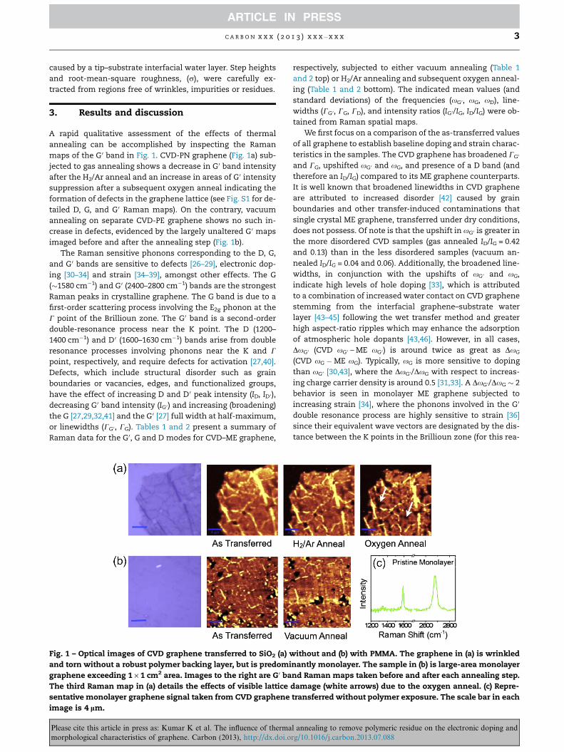
A rapid qualitative assessment of the effects of thermal
annealing can be accomplished by inspecting the Raman
maps of the G 0 band in Fig. 1. CVD-PN graphene (Fig. 1a) sub-
jected to gas annealing shows a decrease in G 0 band intensity
after the H2/Ar anneal and an increase in areas of G 0 intensity
suppression after a subsequent oxygen anneal indicating the
formation of defects in the graphene lattice (see Fig. S1 for de-
tailed D, G, and G 0 Raman maps). On the contrary, vacuum
annealing on separate CVD-PE graphene shows no such in-
crease in defects, evidenced by the largely unaltered G 0 maps
imaged before and after the annealing step (Fig. 1b).
The Raman sensitive phonons corresponding to the D, G,
and G 0 bands are sensitive to defects [26–29], electronic dop-
ing [30–34] and strain [34–39], amongst other effects. The G
(�1580 cm�1) and G 0 (2400–2800 cm�1) bands are the strongest
Raman peaks in crystalline graphene. The G band is due to a
first-order scattering process involving the E2g phonon at the
C point of the Brillioun zone. The G 0 band is a second-order
double-resonance process near the K point. The D (1200–
1400 cm�1) and D 0 (1600–1630 cm�1) bands arise from double
resonance processes involving phonons near the K and C
point, respectively, and require defects for activation [27,40].
Defects, which include structural disorder such as grain
boundaries or vacancies, edges, and functionalized groups,
have the effect of increasing D and D 0 peak intensity (ID, ID 0),
decreasing G 0 band intensity (IG0) and increasing (broadening)
the G [27,29,32,41] and the G 0 [27] full width at half-maximum,
or linewidths (CG0, CG). Tables 1 and 2 present a summary of
Raman data for the G 0, G and D modes for CVD–ME graphene,
Fig. 1 – Optical images of CVD graphene transferred to SiO2 (a) w
and torn without a robust polymer backing layer, but is predomi
graphene exceeding 1 · 1 cm2 area. Images to the right are G 0 ba
The third Raman map in (a) details the effects of visible lattice
sentative monolayer graphene signal taken from CVD graphene
image is 4 lm.
Please cite this article in press as: Kumar K et al. The influence of thermamorphological characteristics of graphene. Carbon (2013), http://dx.doi.o
respectively, subjected to either vacuum annealing (Table 1
and 2 top) or H2/Ar annealing and subsequent oxygen anneal-
ing (Table 1 and 2 bottom). The indicated mean values (and
standard deviations) of the frequencies (xG0, xG, xD), line-
widths (CG 0, CG, CD), and intensity ratios (IG0/IG, ID/IG) were ob-
tained from Raman spatial maps.
We first focus on a comparison of the as-transferred values
of all graphene to establish baseline doping and strain charac-
teristics in the samples. The CVD graphene has broadened CG0
and CG, upshifted xG0 and xG, and presence of a D band (and
therefore an ID/IG) compared to its ME graphene counterparts.
It is well known that broadened linewidths in CVD graphene
are attributed to increased disorder [42] caused by grain
boundaries and other transfer-induced contaminations that
single crystal ME graphene, transferred under dry conditions,
does not possess. Of note is that the upshift in xG0 is greater in
the more disordered CVD samples (gas annealed ID/IG = 0.42
and 0.13) than in the less disordered samples (vacuum an-
nealed ID/IG = 0.04 and 0.06). Additionally, the broadened line-
widths, in conjunction with the upshifts of xG 0 and xG,
indicate high levels of hole doping [33], which is attributed
to a combination of increased water contact on CVD graphene
stemming from the interfacial graphene–substrate water
layer [43–45] following the wet transfer method and greater
high aspect-ratio ripples which may enhance the adsorption
of atmospheric hole dopants [43,46]. However, in all cases,
DxG0 (CVD xG 0 – ME xG0) is around twice as great as DxG
(CVD xG �ME xG). Typically, xG is more sensitive to doping
than xG 0 [30,43], where the DxG0/DxG with respect to increas-
ing charge carrier density is around 0.5 [31,33]. A DxG0/DxG � 2
behavior is seen in monolayer ME graphene subjected to
increasing strain [34], where the phonons involved in the G 0
double resonance process are highly sensitive to strain [36]
since their equivalent wave vectors are designated by the dis-
tance between the K points in the Brillioun zone (for this rea-
ithout and (b) with PMMA. The graphene in (a) is wrinkled
nantly monolayer. The sample in (b) is large-area monolayer
nd Raman maps taken before and after each annealing step.
damage (white arrows) due to the oxygen anneal. (c) Repre-
transferred without polymer exposure. The scale bar in each
l annealing to remove polymeric residue on the electronic doping andrg/10.1016/j.carbon.2013.07.088

Table 1 – Mean values of linewidths (C), frequencies (x) and intensity ratios of the G 0, G, and D bands in CVD graphenesubjected to vacuum annealing (top) and gas annealing (bottom). Mean values were taken from 50 points on each sample.Corresponding errors are one standard deviation from the mean.
Process step Type CG0 (cm�1) xG 0 (cm�1) CG (cm�1) xG (cm�1) CD (cm�1) xD (cm�1) IG0/IG ID/IG
As transferred PE 30.3 ± 1.9 2679.2 ± 1.8 16.9 ± 1.0 1585.6 ± 1.0 70.5 ± 10.7 1351.3 ± 2.3 1.62 ± 16 0.06 ± 0.05Vacuum annealed 31.6 ± 2.2 2679.4 ± 1.8 18.6 ± 1.6 1585.7 ± 1.4 72.6 ± 5.5 1345.3 ± 1.0 1.71 ± 0.15 0.09 ± 0.02
As transferred PN 29.2 ± 1.2 2676.9 ± 1.8 15.0 ± 1.0 1584.9 ± 0.8 58.1 ± 13.1 1343.3 ± 4.6 1.53 ± 0.04 0.04 ± 0.01Vacuum annealed 32.5 ± 1.6 2681.9 ± 1.5 13.3 ± 1.1 1587.0 ± 1.0 56.2 ± 5.1 1351.2 ± 3.0 1.48 ± 0.17 0.10 ± 0.03
As transferred PE 30.6 ± 2.1 2680.3 ± 1.9 18.6 ± 1.1 1585.5 ± 1.2 53.1 ± 8.0 1345.0 ± 4.8 1.38 ± 0.26 0.419 ± 0.31H2/Ar annealed 39.3 ± 1.8 2683.0 ± 1.1 27.8 ± 2.6 1590.4 ± 3.0 85.0 ± 6.5 1356.9 ± 5.5 0.9 ± 0.05 0.801 ± 0.03Oxygen annealed 42.8 ± 1.5 2683.7 ± 1.1 19.9 ± 2.9 1598.5 ± 3.0 35.3 ± 4.8 1344.6 ± 2.7 1.17 ± 0.21 0.425 ± 0.35
As transferred PN 29.7 ± 1.8 2678.8 ± 1.0 17.3 ± 1.6 1584.5 ± 0.4 63.0 ± 8.6 1343.9 ± 3.5 1.35 ± 0.11 0.13 ± 0.03H2/Ar annealed 44.3 ± 3.0 2685.4 ± 2.3 33.3 ± 3.2 1589.0 ± 0.8 78.4 ± 7.7 1359.8 ± 5.4 0.73 ± 0.05 0.83 ± 0.05Oxygen annealed 39.6 ± 3.4 2680.8 ± 1.5 22.7 ± 1.9 1592.7 ± 2.0 34.5 ± 9.1 1346.2 ± 2.0 1.24 ± 0.17 0.16 ± 0.06
Table 2 – Mean values of linewidths (C), frequencies (x) and intensity ratios of the G 0, G, and D bands in ME graphenesubjected to vacuum annealing (top) and gas annealing (bottom). The D band was not present in most samples, even afterthermal annealing. Mean values were taken from 25 monolayer to 25 bilayer samples. Corresponding errors are one standarddeviation from the mean.
Process step Type CG 0 (cm�1) xG0 (cm�1) CG (cm�1) xG (cm�1) CD (cm�1) xD (cm�1) IG 0/IG ID/IG
As transferred PE 24.6 ± 0.9 2671.2 ± 0.9 14.2 ± 1.4 1579.7 ± 0.8 22.61 ± 1.2 1351.3 ± 1.1 1.6 ± 0.14 0.53 ± 0.27Vacuum annealed 24.1 ± 1.0 2671.8 ± 1.5 12.9 ± 2.4 1580.7 ± 1.0 22.41 ± 2.3 1345.3 ± 1.0 1.6 ± 0.15 0.52 ± 0.27
As transferred PN 24.3 ± 0.3 2665.9 ± 1.6 13.9 ± 0.4 1578.8 ± 0.8 N/A N/A 1.6 ± 0.03 N/AVacuum annealed 29.0 ± 1.0 2669.5 ± 1.2 17.0 ± 0.8 1581.1 ± 0.4 N/A N/A 1.7 ± 0.03 N/A
As transferred PE 24.6 ± 1.4 2668.1 ± 2.4 12.7 ± 2.4 1580.3 ± 1.4 N/A N/A 2.7 ± 0.39 N/AH2/Ar annealed 31.1 ± 2.9 2678.6 ± 4.1 11.3 ± 2.0 1589.4 ± 2.8 N/A N/A 0.9 ± 0.15 N/AOxygen annealed 32.7 ± 3.0 2678.2 ± 4.5 11.6 ± 2.8 1591.2 ± 1.7 N/A N/A 1.0 ± 0.15 N/A
As transferred PN 24.8 ± 1.4 2666.3 ± 3.4 10.0 ± 1.0 1580.8 ± 2.0 N/A N/A 2.3 ± 0.83 N/AH2/Ar annealed 33.1 ± 2.9 2676.3 ± 3.8 12.6 ± 1.3 1589.0 ± 2.7 N/A N/A 0.7 ± 0.17 N/AOxygen annealed 30.1 ± 2.9 2671.9 ± 3.3 11.5 ± 1.1 1591.3 ± 1.7 N/A N/A 0.9 ± 0.21 N/A
4 C A R B O N x x x ( 2 0 1 3 ) x x x – x x x
son, xD is also highly sensitive to strain). In this case, how-
ever, the comparison is between CVD–ME graphene with dif-
fering levels of relative strain. A recent work by Bissett et al.
[38], compared the effects of strain on CVD–ME graphene
and showed that, for increasing compressive strain until
�0.21%, the G peak of CVD graphene is upshifted with respect
to that of ME graphene, with the G 0 band showing a similar 2·increase with increasing compressive strain for both CVD–ME
graphene [38]. This difference in strain between CVD–ME
unexposed to PMMA may arise from the wrinkle-inducing
post-transfer water evaporation in CVD graphene. Table 1 fur-
ther demonstrates the similarities of the as-transferred val-
ues of xG0, xG, CG 0, and CG to within one standard deviation,
between the CVD graphene subjected to gas annealing and
the CVD graphene subjected to vacuum annealing. These re-
sults are a measure of material homogeneity between various
locations of the pristine monolayer graphene. As mentioned
above, all defects such as vacancies, grain boundaries and
transfer contaminations would activate the D band, ensuring
a baseline D band value. Given this baseline and despite the
homogeneity of the G and G 0 peaks between samples, the
as-transferred graphene subjected to gas annealing is more
Please cite this article in press as: Kumar K et al. The influence of thermamorphological characteristics of graphene. Carbon (2013), http://dx.doi.o
defective than that subjected to vacuum annealing, illus-
trated by the greater mean ID/IG ratio (0.04 vs 0.13 for PN
and 0.06 vs 0.42 for PE) and lesser mean IG 0/IG ratio (1.53 vs
1.35 for PN and 1.62 vs 1.38 for PE). This greater defectiveness,
due to variation in graphene domain size, was not found to
significantly affect the annealing-induced shifts in peak
parameters. We find that the as-transferred values of CVD-
PE xG0 and, xG are slightly upshifted, just outside one stan-
dard deviation, indicating a relative increase in hole doping,
with respect to the CVD-PN xG0 andxG values. This is consis-
tent with a previous study by Pirkle et al., where FET measure-
ments showed that exposure to PMMA induced hole doping in
CVD graphene [17]. We also find this behavior occurring in the
ME graphene in Table 2, where the ME-PE G and G 0 bands are
upshifted with respect to the ME-PN values, outside one stan-
dard deviation, further confirming that PMMA is a source of
hole doping in graphene transferred to a SiO2 substrate.
We now examine Tables 1 (top) and 2 (top), respectively,
which detail Raman peak parameter changes in CVD–ME
graphene due to vacuum annealing. It is immediately appar-
ent that the mean CG0, CG, xG0 and xG post-anneal shifts from
the CVD-PE and ME-PE graphene are negligible, being within
l annealing to remove polymeric residue on the electronic doping andrg/10.1016/j.carbon.2013.07.088

C A R B O N x x x ( 2 0 1 3 ) x x x – x x x 5
one standard deviation, whereas the mean post-anneal shifts
from the CVD-PN and ME-PN are more significant. To further
investigate this, we study the Raman spectra from represen-
tative CVD-PE, CVD-PN, ME-PE and ME-PN graphene in
Fig. 2. Post-anneal G 0 band alteration of both CVD–ME poly-
mer exposed graphene is negligible while that of the PN
graphene is considerably broadened and stiffened (CVD
DCG0 = 5.0 cm�1, DxG0 = 6.7 cm�1 and ME DCG0 = 3.9 cm�1,
DxG0 = 3.4 cm�1) The G band of the CVD-PE graphene broadens
(+1.3 cm�1) and stiffens (+1.8 cm�1) slightly, while that of the
ME-P graphene sharpens (�2.1 cm�1) and stiffens insignifi-
cantly (+0.5 cm�1). The G band slightly sharpens for the
CVD-PN graphene (�0.6 cm�1) and broadens for the ME-PN
graphene (+2.4 cm�1) with stiffening in both cases (CVD
DxG = 3.9 cm�1 and ME DxG = 1.6 cm�1).
Vacuum annealing of PE graphene is expected to desorb
PMMA residues [17,18] and other atmospheric contaminants.
This would result in a softening of xG0 and xG as hole dopants
are removed, which would be observed if the Raman spectra
of the samples were measured in vacuum [17,47]. However,
upon exposure to atmospheric conditions after the vacuum
annealing, the G and G 0 bands (i.e., post-annealing values)
would stiffen compared to pre-annealing values [47]. This
change is not clearly observed in our experiments from the
post-anneal values; the G band positions, especially being
more sensitive to charge doping, are almost the same as the
Fig. 2 – Raman spectra of (a) pristine CVD graphene and (b) ME
annealing. Graphs to right are magnifications of the G and G 0 pe
the solid lines correspond to (1) and dotted lines to (2).
Please cite this article in press as: Kumar K et al. The influence of thermamorphological characteristics of graphene. Carbon (2013), http://dx.doi.o
as-transferred values and largely within variation of spectral
values. We discuss several processes that could account for
this effect. Initially, the removal of PMMA would reduce hole
doping, but uncover sites where atmospheric H2O or O2 could
adsorb and then increase hole doping [43,47]. Next, any ther-
mal annealing process (including gas annealing) removes the
interfacial water layer between the graphene and substrate,
decreasing H2O-assisted hole doping [44,45] and thus brings
the graphene layer closer to the substrate, increasing n-type
charge injection from the substrate [48]. As the graphene
layer conformably contacts the corrugated SiO2, the distortion
of the lattice would relax short range C–C bonds and allow in-
creased chemical reactivity [49], especially in the grain
boundaries [50], to adsorbates such as atmospheric hole do-
pants. Overall, the net effect would be to maintain charge
doping in the graphene layer as we discern above. Any minor
strain effects from the conformal SiO2 contact in CVD-PE
graphene (stiffened G 0 and softened G with compressive
strain) [38] would then be overwhelmed by the shifts from
doping.
AFM measurements confirm many of these processes
(Fig. 3). PMMA is clearly burned away as evidenced by the de-
creased step heights and r values of the CVD-PE graphene
post-anneal (Fig. 3a). We also confirm the thermal annealing
removal of the interfacial water layer from all CVD graphene
by the AFM step height reduction in a CVD-PN graphene sam-
monolayer graphene taken (1) before and (2) after vacuum
aks clearly showing peak position and intensity shifts. Here
l annealing to remove polymeric residue on the electronic doping andrg/10.1016/j.carbon.2013.07.088

Fig. 3 – Non-contact mode AFM topographic images and line scans of (a) CVD-PE graphene, (b) CVD-PN graphene, and (c) ME-
PN graphene taken (1) before and (2) after vacuum annealing. The boxes in the left-hand side images show regions where
roughness (r) measurements were taken. In (a), averaged line scans show a decrease in step height from 2.87 to 0.53 nm as
polymeric residue is removed. This effect is noticeable in the 3-D image on the right as rCVD-PE decreases from 0.50 to
0.29 nm. The annealing effect on the step height is seen in the line scans of (b) as CVD-PN graphene height decreases from
0.77 to 0.34 nm. The 3-D images on the right detail the effect of graphene conforming to the substrate. In the location marked
by the arrow, the graphene is largely indistinguishable from the substrate. The rSiO2and rCVD-PN is 0.64 and 1.12 nm,
respectively in (1) and 0.16 and 0.24 nm, respectively in (2). Line scans and images in (c) illustrate the annealing effect of
conformal contact with the substrate in ME-PN graphene. The AFM detector is unable to clearly distinguish graphene and
substrate, and post-annealing rSiO2and rME-PN are 0.25 and 0.27 nm, respectively. These scans corroborate that as-transferred
step heights are larger for CVD-PN graphene than for ME-PN graphene due to the larger interfacial graphene–substrate layer
in CVD samples from water exposure during the transfer process. Because ME graphene does not have an interfacial layer to
this extent, it is able to conform dramatically to the substrate upon annealing. The dotted lines in the 2-D images in (b) and (c)
are a guide showing the edge of the graphene layer post vacuum anneal. The scale bars in the 2-D images in (a), (b), and (c) are
1 lm, 1 lm, and 625 nm, respectively. The 3-D scans are all 2.5 · 2.5 lm2.
6 C A R B O N x x x ( 2 0 1 3 ) x x x – x x x
ple (Fig. 3b), which has no polymer residue to mask the true
height values. AFM scans of ME-PN graphene further corrob-
orate exceptional conformal contact with the corrugated
SiO2 substrate (Fig. 3c); here the graphene is indistinguishable
from the substrate except at the sample edge and surface
roughness values match that of the underlying SiO2. This con-
tact was more pronounced in ME-PN graphene due to the
smaller interfacial water layer and less transfer-induced com-
pressive strain (see previous section) than CVD-PN graphene,
although it can be seen in some regions of the CVD-PN AFM
scan (Fig. 3b).
The important processes affecting the Raman spectra in
CVD-PN and ME-PN graphene are thus removal and re-
adsorption of surface contaminants, removal of the interfa-
cial water layer, increased reactivity of graphene due to closer
conformal contact to, and minor charge injection from the
substrate. The stiffening of the G peak and decrease of IG 0/IGin the CVD-PN graphene are consistent with an increase in
hole doping [33], although the greater increase of G 0 peak po-
sition signifies the effect of approximately 0.1% compressive
strain [38]. Here, the G peak position stiffening from hole dop-
ing would be in competition from the softening which would
occur under this compressive strain. The DxG0/DxG in the ME-
PN graphene is also indicative of compressive strain from
thermal cycling (0.05%) [34,38]. However, if this compressive
strain also exists in the polymer exposed CVD or ME graphene
Please cite this article in press as: Kumar K et al. The influence of thermamorphological characteristics of graphene. Carbon (2013), http://dx.doi.o
after the thermal cycling, its effects would be neutralized in
the Raman spectra from the influence of charge doping as
mentioned above or from smaller localized deformation since
the PE samples never quite reach the conformal contact levels
of PN graphene (Fig. 3a vs b). We also note that IG0/IG increased
and ID/IG decreased for all polymer exposed graphene consis-
tent with the removal of polymeric functional groups [27,51],
however, the increase in CD of the CVD-PE graphene indicates
a general increase in lattice disorder upon annealing. A more
detailed study of the effect of thermal annealing on sheet dis-
order needs to be performed in the future to elucidate the
cause of this width increase.
We now examine Tables 1 (bottom) 2 (bottom), respec-
tively, which detail Raman peak parameter changes in CVD–
ME graphene due to H2/Ar annealing and subsequent oxygen
annealing. Of immediate note is the drastic broadening and
substantial stiffening of all CVD Raman peaks after H2/Ar
annealing. Similar effects are seen in ME graphene, with dras-
tic peak stiffening and significant peak broadenings (except
the mean ME-PE G band sharpening by 1.4 cm�1). The repre-
sentative spectra (Fig. 4a) of CVD graphene show a broad fluo-
rescent signal from 1200 to 1650 cm�1 superimposed upon the
greatly broadened D and G peaks and the suppressed G 0 peak
after the H2/Ar anneal for both CVD-PE and CVD-PN graph-
ene. This signal may evidently be attributed purely to the
existence of amorphous carbon (mixture of sp2- and sp3-
l annealing to remove polymeric residue on the electronic doping andrg/10.1016/j.carbon.2013.07.088

1
2
3
CVD - PE(a) (b) ME - PE
(c)
1 2
ME-PE
CVD-PE
Edge contamination
(d)Δ = 4.51
Δ = 0.91Δ = 1.46
CVD - PN ME - PN
Fig. 4 – Raman spectra of (a) pristine CVD graphene and (b) ME monolayer graphene taken (1) before H2/Ar annealing, (2) after
H2/Ar annealing and (3) after oxygen annealing. AFM images and line scans (c) of CVD-PE graphene showing increase in step
height to 4.51 nm caused by scission of PMMA after (2). Residue removal occurs during (3), bringing the step height down to
0.91 nm. The scale bar is 1.5 lm. AFM images (d) of ME-PE and CVD-PE graphene (1) before and (2) after H2/Ar annealing
showing edge contamination only on the ME graphene, but a layer of residue atop the CVD graphene. The images are
2.5 · 2.5 lm2. The r measurements were taken from the boxed areas. rSiO2and rME-PE is 0.18 and 0.22 nm, respectively in (1)
and could not be measured post anneal due to scanning artifacts from edge contamination. rSiO2and rCVD-PE is 0.32 and
0.48 nm, respectively in (1) and 0.36 and 2.56 nm, respectively in (2).
C A R B O N x x x ( 2 0 1 3 ) x x x – x x x 7
bonded carbon) from the scission of PMMA [21,52–54] which is
not largely removed as in vacuum annealing. Indeed, Lin et al.
[11] report that a similar signal arises when PMMA-trans-
ferred graphene is suspended, and is dampened after several
H2/Ar and oxygen anneals, as the PMMA is removed. We agree
that the signal is partially due to the existence of amorphous
carbon as evidenced by the drastic broadening of the D peak
and increase of the CVD ID/IG signal to �0.80 [42,55–57], fur-
ther noting the presence of this residue in AFM scans
(Fig. 4c) of CVD-PE graphene. However, here we see this signal
arise in graphene transferred both with and without PMMA
post-H2/Ar anneal. Therefore, we attribute the fluorescence
and increased disorder to the functionalization of graphene
with H2 and other contaminants forming sp3 sites during
the annealing process [42,58]. This sp3 functionalization is
known to superimpose a strong fluorescent peak in carbon
with high hydrogen content [57,59]. Interestingly, there is a
weaker fluorescent signal and suppressed G 0 peak in ME
graphene subjected to H2/Ar anneal (Fig. 4b), but no D band
activation as would occur if hydrogen were creating disor-
dered sp3 sites. However, from Fig. 4, the strong G 0 peak stiff-
ening (ME-PE DxG 0 = 12.3 cm�1 and ME-PN DxG0 = 13.0 cm�1)
and G 0 peak broadening (ME-PE DCG0 = 8.0 cm�1, ME-PN
DCG0 = 6.5 cm�1) coupled with the visible IG 0/IG reduction indi-
cate that the H2/Ar anneal strained [34,38] the graphene, over-
whelming any doping effects from PMMA or contamination
Please cite this article in press as: Kumar K et al. The influence of thermamorphological characteristics of graphene. Carbon (2013), http://dx.doi.o
removal, environmental exposure, and/or conformal contact
with the substrate. AFM scans show residue attached pre-
dominantly to the more reactive edges of the ME graphene
film (Fig. 4d) (not seen in scans of graphene subjected to vac-
uum annealing in Fig. 3c), which we believe is a partial cause
of strain fields (discussed below) within the graphene. This is
unlike the residue spread over the polycrystalline CVD graph-
ene (Fig. 4d) which contains more reactive sites such as
strained grain boundaries [50]. Thus, there is supporting evi-
dence here that pre-existing defects allow or enhance sp3
functionalization; however, research on this defect-enhanced
functionalization and the cause of the fluorescence in the ME
graphene is still ongoing.
Subsequently, upon oxygen annealing, we find that the
fluorescent signal largely disappeared in CVD graphene
(Fig. 4a) and IG 0/IG returned to its original values. However,
the samples are now highly hole-doped as evidenced by the
G 0 and G band stiffening compared to the as-transferred posi-
tions. Interestingly, the CVD-PE CD and xD largely returned to
the as transferred values of �24 cm�1 and �1345 cm�1 with
ID/IG also returning to very close to as transferred values
(0.14 vs pre-annealed 0.16 for CVD-PE and 0.32 vs pre-an-
nealed 0.16 for CVD-PN), pointing to removal of both poly-
meric residue and hydrogen-functionalized sp3 sites
[12,43,58]. The ME graphene did not display this reversibility
(Fig. 4b). Although the fluorescent signal was slightly damp-
l annealing to remove polymeric residue on the electronic doping andrg/10.1016/j.carbon.2013.07.088

(a)
(c)
(b)
P21
P12P22
P11
1
2
3
Fig. 5 – Raman spectra and AFM scans of bilayer ME graphene subjected to gas annealing. (a) Raman spectra taken (1) before
H2/Ar annealing, (2) after H2/Ar annealing, and (3) after oxygen annealing. (b) Zoom-in of G 0 band in (a-1) showing 4 possible
double resonance phonons. Inset is of broad, single peaked G 0 band post H2/Ar anneal. (c) AFM scans of multilayer graphene
taken (1) before H2/Ar annealing, (2) after H2/Ar annealing, and (3) after oxygen annealing. The arrows correspond to where r
was measured over a 250 nm2 box (not shown). Black arrow is on monolayer graphene, blue arrow is on bilayer graphene,
yellow arrow on SiO2 substrate. The rSiO2, rmonolayer, and rbilayer is 0.31, 0.14, and 0.23 nm, respectively in (1) and 0.32 nm, 0.32,
and 0.27 nm, respectively in (3), showing close conformal contact of the monolayer to the corrugated substrate. As in Fig. 3c,
the monolayer region cannot be distinguished from the surrounding substrate. The r measurements were not taken in (2)
because of the scanning artifacts from edge contamination. The 3-D scans are 2.5 · 2.5 lm2. (For interpretation of the
references to color in this figure legend, the reader is referred to the web version of this article.)
8 C A R B O N x x x ( 2 0 1 3 ) x x x – x x x
ened, the IG0/IG values remained near the post H2/Ar anneal
value of 0.9 (compared to the higher pre-anneal values of
2.8 for CVD-PE and 1.6 for CVD-PN).
We now show that the spectral changes in ME graphene
upon H2/Ar anneal are a strain induced effect, which remain
after the oxygen anneal. In bilayer ME graphene (Fig. 5), the
G 0 peak may be fitted using four Lorentzian peaks, corre-
sponding to four double resonance processes, or phonons
(P11, P22, P12, P21 in Fig. 5b). However, after H2/Ar annealing,
the asymmetrical, multi-peaked G 0 line shape typical of AB
stacked bilayer disappears to be replaced by a slightly asym-
metric, single peaked band (Fig. 5b, inset), more typical of a
monolayer or rotated bilayer [60,61]. It has to be noted that
there is no accompanying presence of a D band, indicating
that there are no defects or adsorbed sp3 sites, which may
contribute to the signal. We attribute the appearance of
asymmetric band after H2/Ar annealing to unequal strain
fields between the two graphene layers [37], which would
break the inversion symmetry of the lattice [62,63] and mis-
orient the stacking between the layers. In Fig. 5c, H2/Ar an-
neal-induced edge contamination is visible in an AFM scan
of bilayer graphene with the bottom monolayer region
extending outward from beneath it. The strain signal first
arises after this annealing, presumably due to the edge con-
tamination, however, we were unable to take accurate step
height or roughness measurements due to scan artifacts
Please cite this article in press as: Kumar K et al. The influence of thermamorphological characteristics of graphene. Carbon (2013), http://dx.doi.o
from the contamination. After the oxygen anneal, the poly-
meric contamination is removed, but the strain signal re-
mains. At this point, AFM measurements show that the
monolayer region was highly conformed to the substrate
as to be indistinguishable (Fig. 5c, highlighted) from it. In-
deed, both rSiO2and rmonolayer is 0.32 nm, whereas the bi-
layer is smoother, with r of 0.27 nm. The weaker attraction
[64] between the bottom and top graphene layers in bilayer
in conjunction with the interaction caused by the strong
conformal contact from bottom layer pinning to the sub-
strate is a strong indicator of unequal strain fields between
the layers. Thus, in bilayer graphene, the G 0 band would dis-
play a misoriented peak shape, especially if the underlying
graphene layer conformally contacted the substrate during
the H2/Ar anneal. The second thermal anneal would have
the effect of further pinning the underlying graphene layer
(or single monolayer) to the substrate, thus the strain signal
remains subsequent to oxygen annealing.
4. Conclusions
We have systematically investigated the effect of both gas and
vacuum annealing on the removal of polymer from CVD–ME
graphene and the subsequent electronic and morphological
changes induced in the graphene. Data from Raman spectros-
copy and AFM, combined with previous electrical character-
l annealing to remove polymeric residue on the electronic doping andrg/10.1016/j.carbon.2013.07.088
C A R B O N x x x ( 2 0 1 3 ) x x x – x x x 9
ization, showed that gas annealing introduces partially
reversible changes in the doping levels of CVD graphene from
polymer residue/hydrogen-functionalization, and irreversible
changes in the strain fields of ME graphene from annealing-
induced substrate pinning. This strain effect was confirmed
by subjecting ME bilayer graphene to gas annealing, which in-
duced a significant and irreversible G 0 line shape change from
the 4-peak Bernal shape to a broad, single peak, due to un-
equal strain fields between the graphene layers. On the other
hand, vacuum annealing was found to remove most poly-
meric residue, with only minor doping and straining of the
graphene, making it an attractive alternative to gas anneal-
ing. A comparison of AFM step height and roughness mea-
surements between graphene exposed and unexposed to
polymer elucidated several competing annealing-induced ef-
fects, such as removal of the interfacial graphene–substrate
water layer, conformal contact of the graphene with the sub-
strate, deformation of graphene, and the presence of poly-
meric residue, all of which directly influence doping and
strain in the graphene lattice.
Acknowledgments
The material processing and characterization, including most
Raman spectroscopy and all vacuum annealing, were carried
out at the Center for Functional Nanomaterials, Brookhaven
National Laboratory, which is supported by the U.S. Depart-
ment of Energy, Office of Basic Energy Sciences, under Con-
tract No. DE-AC02-98CH10886. We thank Ye Tian and
Andreas Pallikaras for their help with graphene transfer and
processing. We also thank Dr. Stefan Strauf of the Physics
and Engineering Physics department at Stevens Institute of
Technology for use of his Raman spectroscopy setup when
required.
This work was supported in part by the Robert Crooks
Stanley Fellowship and GK12 Fellowship at Stevens Institute
of Technology. Also, this work has been supported in part by
National Science Foundation (DMR-0922522, EECS-1040007,
ECCS-1104870, and EEC-1138244) and Air Force Office for Sci-
entific Research (FA9550-11-1-0272 and FA9550-12-1-0326).
Appendix A. Supplementary data
Supplementary data associated with this article can be found,
in the online version, at http://dx.doi.org/10.1016/
j.carbon.2013.07.088.
R E F E R E N C E S
[1] Gomez De Arco L, Zhang Y, Schlenker CW, Ryu K, ThompsonME, Zhou C. Continuous, highly flexible, and transparentgraphene films by chemical vapor deposition for organicphotovoltaics. ACS Nano 2010;4(5):2865–73.
[2] Liu W, Jackson BL, Zhu J, Miao CQ, Chung CH, Park YJ, et al.Large scale pattern graphene electrode for high performancein transparent organic single crystal field-effect transistors.ACS Nano 2010;4(7):3927–32.
Please cite this article in press as: Kumar K et al. The influence of thermamorphological characteristics of graphene. Carbon (2013), http://dx.doi.o
[3] Liu JF, Chan KS, Wang J. A bipolar spin-filtering effect ingraphene zigzag nanoribbons with spin–orbit coupling.Nanotechnology 2012;23(9):095201.
[4] Kim YS, Kumar K, Fisher FT, Yang EH. Out-of-plane growth ofCNTs on graphene for supercapacitor applications.Nanotechnology 2011;23(1):015301.
[5] Dan Y, Lu Y, Kybert NJ, Luo A, Johnson ATC. Intrinsic responseof graphene vapor sensors. Nano Lett 2009;9(4):1472–5.
[6] Yang G, Lee C, Kim J, Ren F, Pearton SJ. Flexible graphene-based chemical sensors on paper substrates. Phys ChemChem Phys 2013;15:1798–801.
[7] Chan J, Venugopal A, Pirkle A, McDonnell S, Hinojos D,Magnuson CW, et al. Reducing extrinsic performance-limiting factors in graphene grown by chemical vapordeposition. ACS Nano 2012;6(4):3224–9.
[8] Li X, Cai W, An J, Kim S, Nah J, Yang D, et al. Large-areasynthesis of high-quality and uniform graphene films oncopper foil. Science 2009;324(5932):1312–4.
[9] Ishigami M, Chen JH, Cullen WG, Fuhrer MS, Williams ED.Atomic structure of graphene on SiO2. Nano Lett2007;7(6):1643–8.
[10] Geringer V, Subramaniam D, Michel AK, Szafranek B, SchallD, Georgi A, et al. Electrical transport and low-temperaturescanning tunneling microscopy of microsoldered graphene.Appl Phys Lett 2010;96(8):082114.
[11] Lin YC, Jin C, Lee JC, Jen SF, Suenaga K, Chiu PW. Cleantransfer of graphene for isolation and suspension. ACS Nano2011;5(3):2362–8.
[12] Elias DC, Nair RR, Mohiuddin TMG, Morozov SV, Blake P,Halsall MP, et al. Control of graphene’s properties byreversible hydrogenation: evidence for graphene. Science2009;323(5914):610–3.
[13] Song J, Ko TY, Ryu S. Raman spectroscopy of annealing-induced effects on graphene prepared by micromechanicalexfoliation. arXivorg 2011; cond-mat, DOI 10.5012/bkcs.2010.31.9.2679.
[14] Iqbal MW, Singh AK, Iqbal MZ, Eom J. Raman fingerprint ofdoping due to metal adsorbates on graphene. J Phys: CondensMatter 2012;24(33):335301.
[15] Booth TJ, Blake P, Nair RR, Jiang D, Hill EW, Bangert U, et al.Macroscopic graphene membranes and their extraordinarystiffness. Nano Lett 2008;8(8):2442–6.
[16] Huang Y, Dong X, Shi Y, Li CM, Li LJ, Chen P. Nanoelectronicbiosensors based on CVD grown graphene. Nanoscale2010;2(8):1485–8.
[17] Pirkle A, Chan J, Venugopal A, Hinojos D, Magnuson CW,McDonnell S, et al. The effect of chemical residues on thephysical and electrical properties of chemical vapordeposited graphene transferred to SiO2. Appl Phys Lett2011;99(12):122108.
[18] Cheng Z, Zhou Q, Wang C, Li Q, Wang C, Fang Y. Towardintrinsic graphene surfaces: a systematic study on thermalannealing and wet-chemical treatment of SiO2-supportedgraphene devices. Nano Lett 2011;11(2):767–71.
[19] Moser J, Barreiro A, Bachtold A. Current-induced cleaning ofgraphene. Appl Phys Lett 2007;91(16):163513.
[20] Jeong HK, Kim KJ, Kim SM, Lee YH. Modification of theelectronic structures of graphene by viologen. Chem PhysLett 2010;498(1–3):168–71.
[21] Lin YC, Lu CC, Yeh CH, Jin C, Suenaga K, Chiu PW. Grapheneannealing: how clean can it be? Nano Lett 2012;12(1):414–9.
[22] Cai W, Moore AL, Zhu Y, Li X, Chen S, Shi L, et al. Thermaltransport in suspended and supported monolayer graphenegrown by chemical vapor deposition. Nano Lett2010;10(5):1645–51.
[23] Calizo I, Balandin AA, Bao W, Miao F, Lau CN. Temperaturedependence of the Raman spectra of graphene and graphenemultilayers. Nano Lett 2007;7(9):2645–9.
l annealing to remove polymeric residue on the electronic doping andrg/10.1016/j.carbon.2013.07.088

10 C A R B O N x x x ( 2 0 1 3 ) x x x – x x x
[24] Nemes-Incze P, Osvath Z, Kamaras K, Biro LP. Anomalies inthickness measurements of graphene and few layer graphitecrystals by tapping mode atomic force microscopy. Carbon2008;46(11):1435–42.
[25] Lui CH, Liu L, Mak KF, Flynn GW, Heinz TF. Ultraflat graphene.Nature 2009;462(7271):339–41.
[26] Cancado LG, Jorio A, Ferreira EHM, Stavale F, Achete CA,Capaz RB, et al. Quantifying defects in graphene via Ramanspectroscopy at different excitation energies. Nano Lett2011;11(8):3190–6.
[27] Ferrari AC. Raman spectroscopy of graphene and graphite:disorder, electron–phonon coupling, doping andnonadiabatic effects. Solid State Commun 2007;143(1–2):47–57.
[28] Jorio A, Ferreira EHM, Cancado LG, Achete CA, Capaz RB.Measuring disorder in graphene with Raman spectroscopy.In: Physics and applications of graphene –experiments. InTech; 2011. p. 439–54.
[29] Eckmann A, Felten A, Mishchenko A, Britnell L, Krupke R,Novoselov KS, et al. Probing the nature of defects ingraphene by Raman spectroscopy. Nano Lett2012;12(8):3925–30.
[30] Yan J, Zhang Y, Kim P, Pinczuk A. Electric field effect tuning ofelectron–phonon coupling in graphene. Phys Rev Lett2007;98(16):166802.
[31] Das A, Pisana S, Chakraborty B, Piscanec S, Saha SK,Waghmare UV, et al. Monitoring dopants by Ramanscattering in an electrochemically top-gated graphenetransistor. Nat Nanotechnol 2008;3(4):210–5.
[32] Lazzeri M, Piscanec S, Mauri F, Ferrari A, Robertson J. Phononlinewidths and electron–phonon coupling in graphite andnanotubes. Phys Rev B 2006;73(15):155426.
[33] Kalbac M, Reina-Cecco A, Farhat H, Kong J, Kavan L,Dresselhaus MS. The influence of strong electron and holedoping on the Raman intensity of chemical vapor-depositiongraphene. ACS Nano 2010;4(10):6055–63.
[34] Mohiuddin T, Lombardo A, Nair R, Bonetti A, Savini G, Jalil R,et al. Uniaxial strain in graphene by Raman spectroscopy: Gpeak splitting, Gruneisen parameters, and sampleorientation. Phys Rev B 2009;79(20):205433.
[35] Metzger C, Remi S, Liu M, Kusminskiy SV, Castro Neto AH,Swan AK, et al. Biaxial strain in graphene adhered to shallowdepressions. Nano Lett 2010;10(1):6–10.
[36] Frank O, Mohr M, Maultzsch J, Thomsen C, Riaz I, Jalil R, et al.Raman 2D-band splitting in graphene: theory andexperiment. ACS Nano 2011;5(3):2231–9.
[37] Frank O, Bousa M, Riaz I, Jalil R, Novoselov KS, Tsoukleri G,et al. Phonon and structural changes in deformed Bernalstacked bilayer graphene. Nano Lett 2012;12(2):687–93.
[38] Bissett MA, Izumida W, Saito R, Ago H. Effect of domainboundaries on the Raman spectra of mechanically strainedgraphene. ACS Nano 2012;6(11):10229–38.
[39] Zabel J, Nair RR, Ott A, Georgiou T, Geim AK, Novoselov AK,et al. Raman spectroscopy of graphene and bilayer underbiaxial strain: bubbles and balloons. Nano Lett2012;12(2):617–21.
[40] Ferrari AC, Meyer JC, Scardaci V, Casiraghi C, Lazzeri M, MauriF, et al. Raman spectrum of graphene and graphene layers.Phys Rev Lett 2006;97(18):187401.
[41] Casiraghi C. Probing Disorder and Charged Impurities inGraphene by Raman Spectroscopy. Phys Status Solidi RRL2009;3(6):175–7.
[42] Ferrari A, Robertson J. Interpretation of Raman spectra ofdisordered and amorphous carbon. Phys Rev B2000;61(20):14095–107.
[43] Ryu S, Liu L, Berciaud S, Yu YJ, Liu H, Kim P, et al.Atmospheric oxygen binding and hole doping in deformedgraphene on a SiO2 substrate. Nano Lett 2010;10(12):4944–51.
Please cite this article in press as: Kumar K et al. The influence of thermamorphological characteristics of graphene. Carbon (2013), http://dx.doi.o
[44] Komurasaki H, Tsukamoto T, Yamazak K, Ogino T. Layeredstructures of interfacial water and their effects on Ramanspectra in graphene-on-sapphire systems. J Phys Chem C2012;116(18):10084–9.
[45] Shim J, Lui CH, Ko TY, Yu YJ, Kim P, Heinz TF, et al. Water-gated charge doping of graphene induced by mica substrates.Nano Lett 2012;12(2):648–54.
[46] Boukhvalov DW, Katsnelson MI. Enhancement of chemicalactivity in corrugated graphene. J Phys Chem C2009;113(32):14716–8.
[47] Ni ZH, Wang HM, Luo ZQ, Wang YY, Yu T, Wu YH, et al. Theeffect of vacuum annealing on graphene. J Raman Spectrosc2009;41(5):479–83.
[48] Romero HE, Shen N, Joshi P, Gutierrez HR, Tadigadapa SA,Sofo JO, et al. N-type behavior of graphene supported on Si/SiO2 substrates. ACS Nano 2008;2(10):2037–44.
[49] de Andres PL, Verges JA. First-principles calculation of theeffect of stress on the chemical activity of graphene. ApplPhys Lett 2008;93(17):171915.
[50] Wang B, Puzyrev Y, Pantelides ST. Strain enhanced defectreactivity at grain boundaries in polycrystalline graphene.Carbon 2011;49(12):3983–8.
[51] Dresselhaus MS, Jorio A, Souza Filho AG, Saito R. Defectcharacterization in graphene and carbon nanotubes usingRaman spectroscopy. Philos Trans R Soc A2010;368(1932):5355–77.
[52] Manring LE, Sogah DY, Cohen GM. Thermal degradation ofpoly(methyl methacrylate). 3: Polymer with head-to-headlinkages. Macromolecules 1989;22(12):4652–4.
[53] Kashiwagi T, Inaba A, Brown JE, Hatada K, Kitayama T,Masuda E. Effects of weak linkages on the thermal andoxidative degradation of poly(methyl methacrylates).Macromolecules 1986;19(8):2160–8.
[54] Costache MC, Wang D, Heidecker MJ, Manias E, Wilkie CA.The thermal degradation of poly(methyl methacrylate)nanocomposites with montmorillonite, layered doublehydroxides and carbon nanotubes. Phys Status Solidi RRL2006;17(4):272–80.
[55] Ferrari AC, Robertson J. Raman spectroscopy of amorphous,nanostructured, diamond-like carbon, and nanodiamond.Philos Trans R Soc A 2004;362(1824):2477–512.
[56] Capano MA, McDevitt NT, Singh RK, Qian F. Characterizationof amorphous carbon thin films. J Vac Sci Technol A1996;14(2):1–5.
[57] Casiraghi C, Ferrari A, Robertson J. Raman spectroscopy ofhydrogenated amorphous carbons. Phys Rev B2005;72(8):085401.
[58] Daniels KM, Daas BK, Srivastava N, Williams C, Feenstra RM,Sudarshan TS, et al. Evidences of electrochemical graphenefunctionalization and substrate dependence by Raman andscanning tunneling spectroscopies. J Appl Phys2012;111:114306–7.
[59] Marchon B, Gui J, Grannen K, Rauch GC, Ager JW, Silva SRP,et al. Photoluminescence and Raman spectroscopy inhydrogenated carbon films. IEEE Trans Magn1997;33(5):3148–50.
[60] Kim K, Coh S, Tan L, Regan W, Yuk J, Chatterjee E, et al.Raman spectroscopy study of rotated double-layer graphene:misorientation-angle dependence of electronic structure.Phys Rev Lett 2012;108(24):246103.
[61] Havener RW, Zhuang H, Brown L, Hennig RG, Park J. Angle-resolved Raman imaging of interlayer rotations andinteractions in twisted bilayer graphene. Nano Lett2012;12(6):3162–7.
[62] Yan J, Villarson T, Henriksen EA, Kim P, Pinczuk A. Opticalphonon mixing in bilayer graphene with a broken inversionsymmetry. Phys Rev B 2009;80(24):241417(R).
l annealing to remove polymeric residue on the electronic doping andrg/10.1016/j.carbon.2013.07.088

C A R B O N x x x ( 2 0 1 3 ) x x x – x x x 11
[63] Mafra DL, Moujaes EA, Doorn SK, Htoon H, Nunes RW,Pimenta MA. A study of inner process double-resonanceRaman scattering in bilayer graphene. Carbon2011;49(5):1511–5.
Please cite this article in press as: Kumar K et al. The influence of thermamorphological characteristics of graphene. Carbon (2013), http://dx.doi.o
[64] Palser AHR. Interlayer interactions in graphite and carbonnanotubes. Phys Chem Chem Phys 1999;1:4459–64.
l annealing to remove polymeric residue on the electronic doping andrg/10.1016/j.carbon.2013.07.088