Embed Size (px)
Citation preview

The How To’s of Metric Driven Verification to Maximize Productivity
Author/Prensenter: Matt Graham
Author: John Brennan
Cadence Design Systems, Inc.
© Accellera Systems Initiative 1

Cadence Design Systems, Inc.
DVCon Europe – Munich, Germany
October 14, 2014
The How To’s of Metric Driven Verification to Maximize Productivity

3 © 2014 Cadence Design Systems, Inc. All rights reserved.
Agenda
Section 1: MDV Methodology IP to SoC Verification
Section 2: MDV Approaches Beyond RTL IP Level
Section 3: Team Based Verification Management
Section 4: MDV In Action

4 © 2014 Cadence Design Systems, Inc. All rights reserved.
But – this is not the end
of the story, next comes
SOC level verification
and associated challenges
IP/Subsystem UVM e/SV Metric Driven VerificationMain Verification Flow Being Adopted Past 15 years
Metric Driven Verification Environment
AutomaticStimulus
Generation
Data and AssertionCheckers
BFM Signal Layer
Coverage Monitor
StimulusSequences
Customer’s Application Specific ComponentsCPU subsystem
3
D
Gr
ap
hi
cs
C
or
e
D
S
P
A/
V
High speed, wired interface peripherals
D
D
R
3
P
H
Y
Other peripherals
S
A
T
AMI
PI
H
D
MI
W
L
A
NL
T
E
Low-speed peripheral
subsystem
Low speed peripherals
P
M
UM
I
P
IJ
T
A
G
I
N
T
CI
2
CS
P
IT
i
m
e
r
G
P
I
O
D
i
s
p
l
a
y
U
A
R
T
Applica
tion
Acceler
ators
…
A
E
S
…
Fabric
CPU
I $
D $
CPU
I $
D $
L2 cache
USB3.0
3
.
0
P
H
Y
2
.
0
P
H
Y
PCIe
Gen
2,3
PHY
E
t
h
e
r
-
n
e
t
P
H
Y
Customer’s Application Specific ComponentsCPU subsystem
3
D
Gr
ap
hi
cs
C
or
e
D
S
P
A/
V
High speed, wired interface peripherals
D
D
R
3
Other peripherals
S
A
T
AMI
PI
H
D
MI
W
L
A
NL
T
E
Low-speed peripheral
subsystem
Low speed peripherals
P
M
UM
I
P
IJ
T
A
G
I
N
T
CI
2
CS
P
IT
i
m
e
r
G
P
I
O
D
i
s
p
l
a
y
U
A
R
T
Applica
tion
Acceler
ators
…
A
E
S
…
Fabric
CPU
I $
D $
CPU
I $
D $
L2 cache
USB3
.0
3
.
0
P
H
Y
2
.
0
P
H
Y
PCIeGen 2,3
PHY
P
H
Y
Customer’s Application Specific ComponentsCPU subsystem
3
D
Gr
ap
hi
cs
C
or
e
D
S
P
A/
V
High speed, wired interface peripherals
D
D
R
3
P
H
Y
Other peripherals
S
A
T
AMI
PI
H
D
MI
W
L
A
NL
T
E
Low-speed peripheral
subsystem
Low speed peripherals
P
M
UM
I
P
IJ
T
A
G
I
N
T
CI
2
CS
P
IT
i
m
e
r
G
P
I
O
D
i
s
p
l
a
y
U
A
R
T
Applica
tion
Acceler
ators
…
A
E
S
…
Fabric
CPU
I $
D $
CPUI $
D $
L2 cache
USB3.0
3
.
0
P
H
Y
2
.
0
P
H
Y
PCIeGen 2,3
PHY
E
t
h
e
r
-
n
e
t
P
H
Y
SoC XYZ
DesignIP
SystemVerilog or e
RTL Simulator
Verify IP exhaustively
should work in ANY
SoC context

5 © 2014 Cadence Design Systems, Inc. All rights reserved.
SoC HW/SW Integration & Verification Challenges
Customer’s Application Specific Components
SoC Interconnect Fabric
ARM CPU Subsystem
3D
Graphics
Core
Modem
High speed, wired interface peripherals
DDR3
PHY
Other peripherals
SATA
MIPI
HDMI
WLAN
LTE
Low-speed peripheral
subsystem
Low speed peripherals
PMU
MIPI
JTAG
INTC
I2C
SPI
Timer
GPIO
Display
UART
Application
Accelerator
s
…
AES
…
A15
L2 cache
USB3.0
3.
0PH
Y
2.
0PH
Y
PCIe
Gen 2,3
PHY
Ether
net
PHY
A15 A7
L2 cache
A7
Cache Coherent Fabric
SoC Coherent and Non-
Coherent Interconnect
Complexity key to
System Performance
Multi-core SW development and
HW/SW verification
SoC SW and IP
integration with 10’s
to 100’s of IPs
Requires many
development
environments on
different platforms
Complex low-power design features need to
be verified at SoC level
spanning HW/SWTiming, CDC, clk/reset (x-propagation),
gate-level simulation
Integration of
Analog-mixed
signal

6 © 2014 Cadence Design Systems, Inc. All rights reserved.
Need for Concurrent HW/SW DevelopmentShift Left
Block Chip PrototypeSilicon
lab test Field test
ROM
ContentDrivers / RTOS / Applications
Diagnostics
& FirmwareHW/SW
Spec
Serial HW->SW Development
Block Chip PrototypeSilicon
lab test Field test
ROM
ContentDrivers / RTOS / Applications
Diagnostics
& FirmwareHW/SW
Spec
Time to market
advantage
Concurrent HW->SW Development
• Integrate HW/SW early and often
• HW designed and verified in SW context
• Software exposed early to HW spec changes
• Verify SoC can support required SW applications
7 © 2014 Cadence Design Systems, Inc. All rights reserved.
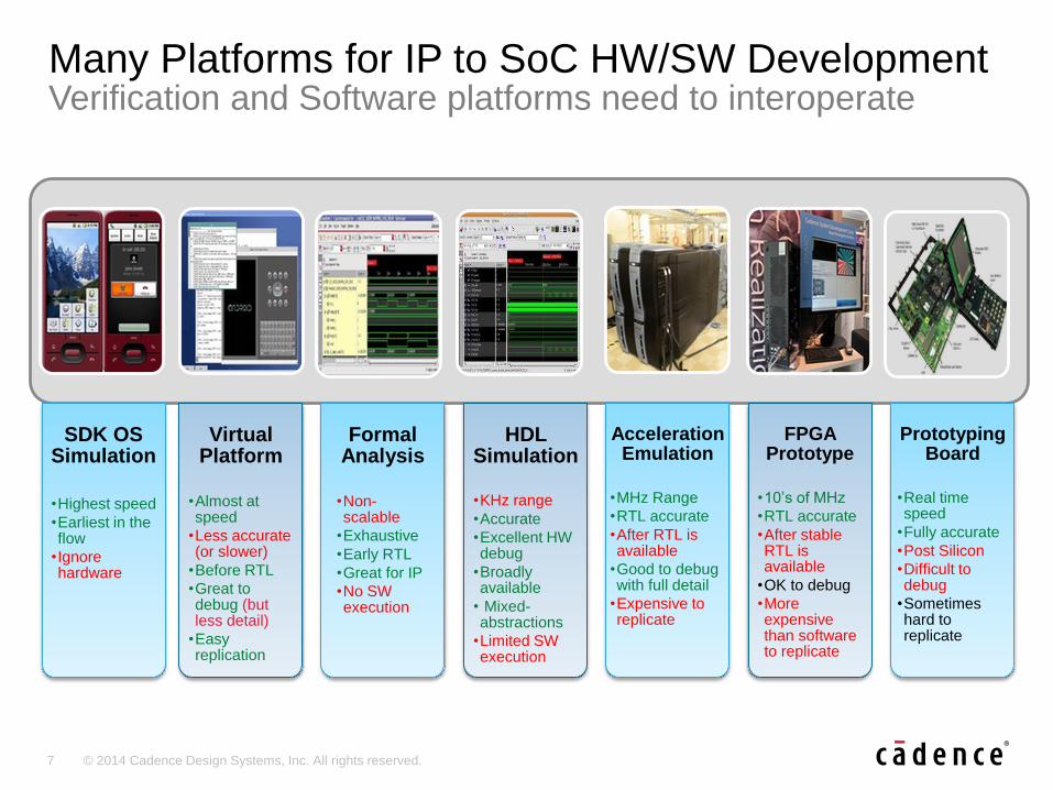
Many Platforms for IP to SoC HW/SW DevelopmentVerification and Software platforms need to interoperate
SDK OS Simulation
•Highest speed
•Earliest in the flow
•Ignore hardware
Virtual Platform
•Almost at speed
•Less accurate (or slower)
•Before RTL
•Great to debug (but less detail)
•Easy replication
Formal Analysis
•Non-scalable
•Exhaustive
•Early RTL
•Great for IP
•No SW execution
HDL Simulation
•KHz range
•Accurate
•Excellent HW debug
•Broadly available
• Mixed-abstractions
•Limited SW execution
AccelerationEmulation
•MHz Range
•RTL accurate
•After RTL is available
•Good to debug with full detail
•Expensive to replicate
FPGA Prototype
•10’s of MHz
•RTL accurate
•After stable RTL is available
•OK to debug
•More expensive than software to replicate
Prototyping Board
•Real time speed
•Fully accurate
•Post Silicon
•Difficult to debug
•Sometimes hard to replicate

8 © 2014 Cadence Design Systems, Inc. All rights reserved.
Challenges with Many Disconnected SoC Development Environments
FPGA
Platform
HW Accel
Emulation
Platform
Simulation
Platform
Virtual
Platform
Develop high speed abstract
C/C++/SystemC Environment
for early SW Development &
Architectural Analysis
Develop IP, Subsystem,
& SoC RTL Verification
Environments
Develop SubSystem,
SoC RTL & HW/SW
Integration Verification
Environments
Develop high speed accurate
FPGA Prototype
Environment for SW
Development & Validation• Many specialized engineering resources required
• Significant development effort for each environment
• Limited sharing of models/VIP between environments
• Difficult to reuse tests across environments
• A lot of effort to migrate between environments

9 © 2014 Cadence Design Systems, Inc. All rights reserved.
IP to SoC HW/SW Integration & Verification Flows
Applications
(Basic to Angry
Birds)
IP
Sub-System
OS & Drivers
(Linux, Android)
Bare Metal SW
System on Chip
Middleware
(Graphics, Audio)
Spec Silicon
IP UVM e/SV Metric Driven Verification
Subsystem UVM e/SV Metric Driven Verification
SoC IP Integration Verification
SoC HW/SW Use Case Verification
SoC HW/SW Integration Verification & Architecture Analysis
SoC Interconnect UVM e/SV Metric Driven Verification & Performance Analysis
Gate Level Verification
Metr
ic D
riven V
erification P
lannin
g
& M
an
ag
em
en
t
UVM e/SV
Coverage Driven
Verification
SW-Driven
Verification
Hybrid
HW/SW
Integration
Register Map
Validation
SoC Connectivity
Verification
Coverage
Unreachability Analysis
Formal Assertion
Based Verification
TLM Design &
Verification

10 © 2014 Cadence Design Systems, Inc. All rights reserved.
HW Acceleration
& Emulation
Virtual Platform
& Hybrid
IP to SoC Pre-Silicon Verification Platforms
Spec Silicon
Simulation &
Formal
Verification
HW Emulation or
FPGA Prototype
IP UVM e/SV Metric Driven Verification
Subsystem UVM e/SV Metric Driven Verification
SoC IP Integration Verification
SoC HW/SW Use Case Verification
SoC HW/SW Integration Verification & Architecture Analysis
SoC Interconnect UVM e/SV Metric Driven Verification & Performance Analysis
Gate Level Verification

11 © 2014 Cadence Design Systems, Inc. All rights reserved.
• Consistent planning and management across different flows– CDV, Formal, Low Power, AMS, Use Case SW-Driven
• Need to support large-scale, multi-site SoC projects– Scalability of coverage merging and analysis
– Scalability of aggregating & archiving data from different teams & sites
• Consistent metrics support across verification platforms– Simulation, Acceleration, Emulation, Virtual Platform
• Uniform metrics based project tracking from IP to SoC flows– Flexibility to “mine” verification database for customized reporting
Expanding Requirements for Metric Driven Verification
12 © 2014 Cadence Design Systems, Inc. All rights reserved.
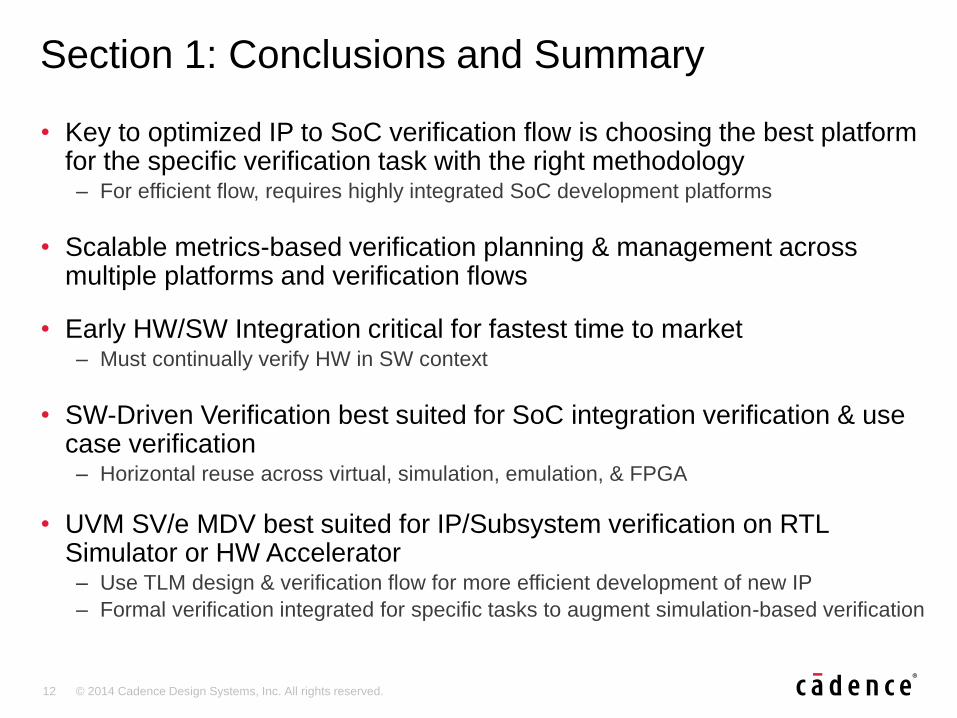
• Key to optimized IP to SoC verification flow is choosing the best platform for the specific verification task with the right methodology– For efficient flow, requires highly integrated SoC development platforms
• Scalable metrics-based verification planning & management across multiple platforms and verification flows
• Early HW/SW Integration critical for fastest time to market– Must continually verify HW in SW context
• SW-Driven Verification best suited for SoC integration verification & use case verification – Horizontal reuse across virtual, simulation, emulation, & FPGA
• UVM SV/e MDV best suited for IP/Subsystem verification on RTL Simulator or HW Accelerator– Use TLM design & verification flow for more efficient development of new IP
– Formal verification integrated for specific tasks to augment simulation-based verification
Section 1: Conclusions and Summary

13 © 2014 Cadence Design Systems, Inc. All rights reserved.
Agenda
Section 1: MDV Methodology IP to SoC Verification
Section 2: MDV Approaches Beyond RTL IP Level
Section 3: Team Based Verification Management
Section 4: MDV In Action

14 © 2014 Cadence Design Systems, Inc. All rights reserved.
MDV: Correlating Metrics with Verification ConcernsData Driven Decisions and Objective Signoff Criteria
98%
Coverage
Grade
Execute Tests
Feature A
Feature B
Feature C
View
Coverage
68%Overall
Grade
Organize
By a Plan
Roll Up Coverage Results

15 © 2014 Cadence Design Systems, Inc. All rights reserved.
Planning is Essential
2. Plan Provides Feature Based Tracking of Progress• Implemented metrics to concretely measure Goals
• Regression results annotated back to Plan Features
1. Plan Specifies Metrics Required for DUT Features:Verification Goals based on:
• Analysis of specifications
• Experience of the team
DUT Feature-Based Plan
• Input Interface A
Coverage & check requirements
• Core Function B
Coverage & check requirements
• Output Interface C
Coverage & check requirements
66%
100%
33%
DUT

16 © 2014 Cadence Design Systems, Inc. All rights reserved.
Benefits of an Executable Feature-based Plan
Without a vPlan, all coverage appears flat
Difficult to correlate to verification plan
Difficult to differentiate between high
priority and lower priority coverage
Without a vPlan
(Coverage Driven Verification)
With a vPlan
(Plan based Metric Driven Verification)
• With a vPlan, sections can be created to organize
by feature areas of interest
• Various types of coverage/check metrics can be
mapped to each section
• Very easy to measure progress relative to your
plan and priorities

17 © 2014 Cadence Design Systems, Inc. All rights reserved.
• Verification Concerns– Interface protocol compliance
– IP/Subsystem configuration, operations, and data paths
– Low power modeling
– Micro-architecture design features
– Stress testing of complex traffic scenarios
• Create UVM e/SV IP/Subsystem Verification Environment– Augment with formal for block level and RTL linting
– Commercial interface VIP for standard protocols
– Reuse interface UVCs for proprietary protocols
– Constrained-random stimulus sequences
– Reference model, register modeling, and scoreboard for data checking
– Assertions for protocol checking
– Functional coverage for measuring features exercised
– Code coverage for measuring HDL implementation exercised– Formal unreachability analysis of code coverage to reach 100%
– Reuse IP Verification Environments to create Subsystem Testbench
IP/Subsystem Verification Flow ConcernsMust be very thorough for efficient SoC verification

18 © 2014 Cadence Design Systems, Inc. All rights reserved.
Traditional MDV Methodology IP and Subsystem Verification
vPlan “Goals”
sequencer
scoreboard
transactiontransactionmonitor monitor
stimulus
driverDUT
slave
0x223F stimulus
0XA30E
0X94D7
0XFF78
0X3767
0XCC18
0XDA83
0XBA1F
0X95FB
0X382E
stimulus
stimulus
stimulus
stimulus
stimulus
stimulus
stimulus
stimulus
stimulus
seed new test
coverage collection
check checkcov cov
stimulus sequences
stimulus sequences
stimulus sequences
stimulus sequences

19 © 2014 Cadence Design Systems, Inc. All rights reserved.
• SoC Interconnect includes hierarchy of connectivity across IPs and memories
• Interconnect Functional Verification– Address map and decoding
– Configuration and address remapping
– All Initiator to target paths
– All target from initiator paths
– Multi-protocol transaction transformations
– Cache behavior for cache coherent interconnect
• Interconnect (and Memory subsystem) Performance Verification and analysis– Latency for critical data paths
– Bandwidth and throughput for heavy traffic stress scenarios
– QoS/QVN requirements
– Cache performance for critical use cases
SoC Interconnect Verification & Performance Concerns

20 © 2014 Cadence Design Systems, Inc. All rights reserved.
• Automatic generation of interconnect TB
• Built on UVM-based VIP
• Same Metrics as IP Verification
Design Feature Coverage Metric Platform
Address map and decoding Functional Sim
Configuration and address remapping Functional Sim
All Initiator to all target paths Functional Sim
All target from all initiator paths Functional Sim
Multi-protocol transaction transformations across
interconnect
Functional, Assertion Sim
Cache behavior for cache coherent interconnect Functional, Assertion Sim
SoC Interconnect Verification vPlan
Virtual
Sequence
Interconnect
WorkbenchRouting
Model
PPP
PPP
ICM
PPP
PPP
AAA
AAA
ICM
Cascaded Interconnect
Non-coherent
M
S
M M M M M
S S
Coherent
M
S
M MM M
S S
DDR
Controller
DDR3
UVM TB

21 © 2014 Cadence Design Systems, Inc. All rights reserved.
• Signal Connectivity in SoC– IP connectivity in SoC
– Clock, interrupt, & reset connectivity
– IO Pad connectivity
• IP Configuration, Primary Operations, & Data Path Connectivity in SoC context– SoC clocking & reset modes
– IP access to Memory
– IP I/O access and data path transaction flow
– IP programmer’s view and primary operations from SW Driver API
– IP Interrupt scenarios
• IP Low power integration– Hierarchical low power control and power modes – power shut-off
and voltage configurations
– Low power interconnect and interface – isolation behavior
SoC IP Integration Verification Concerns

22 © 2014 Cadence Design Systems, Inc. All rights reserved.
Design Feature Coverage Metric Platform
IP Connectivity in SoC Formal Assertion,
Toggle
Formal
Sim
Clock, interrupt, & reset connectivity Formal Assertion Formal
IO Pad connectivity Formal Assertion Formal
IP access to Memory Functional, Toggle Sim
IP I/O access and data path transaction flow Functional, Toggle Sim
IP programmer’s view and primary operations from
SW Driver API
Functional Sim
IP Interrupt scenarios Functional, Assertion Sim
SoC boot/initialization scenarios Functional, Assertion Sim/Accel
Hierarchical low power control and power modes –
power shut-off & voltage configs
Functional, Assertion Sim/Accel
Low power interconnect & interface – isolation
behavior
Functional, Assertion Sim/Accel
SoC IP Integration Verification vPlan
23 © 2014 Cadence Design Systems, Inc. All rights reserved.
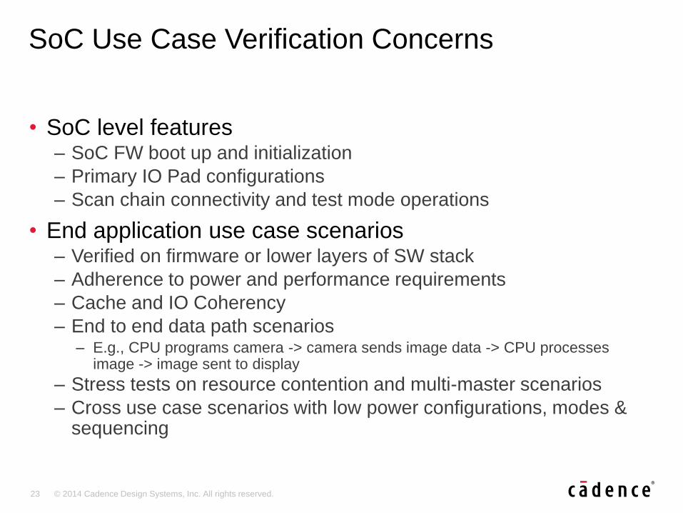
• SoC level features– SoC FW boot up and initialization
– Primary IO Pad configurations
– Scan chain connectivity and test mode operations
• End application use case scenarios – Verified on firmware or lower layers of SW stack
– Adherence to power and performance requirements
– Cache and IO Coherency
– End to end data path scenarios– E.g., CPU programs camera -> camera sends image data -> CPU processes
image -> image sent to display
– Stress tests on resource contention and multi-master scenarios
– Cross use case scenarios with low power configurations, modes & sequencing
SoC Use Case Verification Concerns

24 © 2014 Cadence Design Systems, Inc. All rights reserved.
Design Feature Coverage Metric Platform
SoC FW boot up and initialization Functional, Assertion Sim/Accel
Primary IO Pad configurations Functional, Toggle Sim/Accel
Scan chain connectivity and test mode operations Functional, Assertion Sim/Accel
Cache and IO Coherency Functional, Assertion Sim/Accel
End to end data path scenarios – functional, power,
& performance
Functional, Assertion Sim/Accel
Stress tests on resource contention and multi-
master scenarios
Functional, Assertion Emulation
Cross use case scenarios with low power
configurations, modes & sequencing
Functional, Assertion Emulation
SoC Use Case Verification vPlan

25 © 2014 Cadence Design Systems, Inc. All rights reserved.
• Gate Level Focuses on a critical sub-set of concerns– Tests to be run in zero delay mode
– Reset verification, Initialization, & verification of clocking
– Basic heart beat test to detect functional issues or issues related to X mismatches
– Verify unexpected synthesis transformations
– Validate functional effects after DFT and Low Power insertion
– Tests to be run with timing– Tests to cover/verify STA timing constraints like multi-cycle paths, false paths
– Test to cover asynchronous paths
– Verify DFT with timing
– CDC verification because automatic CDC failing too much at SoC level
– Validation of physical netlist low power implementation
– Safety standards on reliability testing via Fault insertion
• Uses same environment as for SoC Use Case Verification– Except for scan chain verification and other physical netlist artifacts
– Same metrics and engines used as well– Metrics: Black box Functional, Assertion, Toggle
– Engines: Sim/Accel
SoC Gate Level Verification Concerns

26 © 2014 Cadence Design Systems, Inc. All rights reserved.
• Key concerns– Integration & bring-up of OS & higher SW layers on RTL SoC
– Debug integration issues on pre-silicon emulated HW platform
– Validate OS boot up
– Validate middleware and real applications on SoC platform
– Validate performance requirements
– Validate dynamic power usage for critical applications– Based on real running real SW application snippets
– Graphics GPU OpenGL SW API compliance
• Effective Approaches– Use-cases, scenarios, and functional metrics
– Using SW-Driven testbench approaches
– Leverage Emulation & FPGA Prototypes
SoC HW/SW Integration Verification Concerns

27 © 2014 Cadence Design Systems, Inc. All rights reserved.
Quickly establish
test area
Give credit / track
designers work
Effective test
driven verification
environment
MDV Metric OptionsMeasuring the right metrics for the task at hand
MDV Metrics and Approaches
Constrained
Random
Coverage
Driven
Au
tom
ati
on
Eff
ort
Productivity Benefits
Test
CoverageCode
Coverage
Plan
Based
Weeks Months
x
2x
3x
Functional
Testing
Plan
Construct
Execute
Measure /
Analyze
Advanced
Verification
DUT
Functional
CodeTest
Test Driven
Verification
Days
More effort, but
more effective if
resources permit
Leverages
advanced planning
technology
Greater ROI

28 © 2014 Cadence Design Systems, Inc. All rights reserved.
Firmware
ENET x4
APB-Subsystem #1
APB
UART #1 UART #2 SDIO GPIO
Bridge
APB-Subsystem #2
APB
ALUT
Bridge
AHB
SMC
PCM
ARM A9
Power Shut-off Control
SRAM
Ethernet Switch SoC Design
assertions
SoC Verification Metrics Mapped to the Plan
ENET
TBAENET
TBAENET
TBAENET
TBAUART
TBA
assertions
Sim
ula
tio
nA
cce
lera
tio
n Covergroups
covergroups
Mac DriverPower Mgr
Driver
System Controller FW
SW-Driven
TestbenchUse
Cases
Covergroups
assertions
Accelerated
SW-Driven TB

29 © 2014 Cadence Design Systems, Inc. All rights reserved.
Functional
Metrics
SoC MDV Enabler – Multi Engine, Multi Metric PlanExecutable verification plan that can link to all necessary engines and metrics
Assertion
Metrics
Testcase
Metrics

30 © 2014 Cadence Design Systems, Inc. All rights reserved.
Functional
coverage
Code
coverage
SoC MDV Enabler - Manage All Metrics in One Spot Multi Engine, Multi Metric results collection in unified environment
Assertion
coverage
Environment
Hierarchy
Testcase
coverage

31 © 2014 Cadence Design Systems, Inc. All rights reserved.
Agenda
Section 1: MDV Methodology IP to SoC Verification
Section 2: MDV Approaches Beyond RTL IP Level
Section 3: Team Based Verification Management
Section 4: MDV In Action

32 © 2014 Cadence Design Systems, Inc. All rights reserved.
Team MDV: It Still Starts with a Plan!
Code coverage and other metrics
VIP Compliance vPlan
and module level vPlans
Outline from a
Functional SpecLegacy tests
Brainstorming
Heterogeneous
Verification Tools
(ie Formal,Simulation)
The verification plan becomes the anchor to
connect teams and technologies together
Distributed /
Hierarchical
Plans
Requirements
Management
System

33 © 2014 Cadence Design Systems, Inc. All rights reserved.
Plan Composure and Creation: Scalability!
• Long paths mapping metrics to
plan
• Issue compounded across
engines
• Further worsens at great levels
of integration
• Connection to data during plan
composure enables efficiency
• Export/Import to/from popular
formats (XML, CSV, HTML)
enables scripting, publishing, etc
• Resultant plan is mapped
“Correct by construction.”

34 © 2014 Cadence Design Systems, Inc. All rights reserved.
MDV for the SoC Team
• Disparate islands of information
• Inconsistent and incompatible
verification approaches
− Verification methodologies
− Different levels of integration
− Design technologies
• Everyone contributes, but no
single coordinated view of who is
doing what and how
• Goal: provide an independent yet
integrated [multi-user] metric
management and Plan to Closure
methodology
SOC / Integration
Testing
IP Block 2 Tests
IP Block 1 Tests
Connectivity Tests
Advanced
Verification
Hierarchical
Integrated
Plans / Results
Simulation Formal Acceleration Emulation

35 © 2014 Cadence Design Systems, Inc. All rights reserved.
MDV Team
Solution
SoC vPlan
Team MDV – Multi-user, Multi-engine, Multi-analysis
Verification
DB App
SQL DB
IPB1
vPlan
Integ
vPlan
Cnct
vPlan
IPB2
vPlan
IP Block 2 Metrics
(SIM/UVM)
SoC Integration Tests
(SIM/TBA/ICE)
Connectivity Rules
(Formal)
IP Block 1 Metrics
(SIM/UVM)
Hierarchically
Instantiated
Reusable Plans
Metrics stored in
Verification DB

36 © 2014 Cadence Design Systems, Inc. All rights reserved.
Enabling the SoC Verification Team with MDVNext generation MDV Architecture
File
Based
VPM
File
File
FileMerged
File /
Results
• File based data mgmt does not scale
• Data does not inherently stay synchronous
• Single User Environment – Difficult to Share
• Static data – reporting is manual / intensive
• Batch coverage merge not suited to 24/7 runs
• DB gives orders of magnitude greater scaling
• Data synchronicity throughout life of a project
• Multi User Environment – Easy to Share
• Dynamic – fresh data, built-in real time reports
• Continuous operations mode / “always on”
NFS
SQL DB
MDV DB
Application
Client
Client
Client
ClientCoverage/Run
Analysis
Historical
Data
Plan edit
& analyze
Reports
Manager
Dashboard
Client
Clients
Veri
ficati
on
En
gin
es
Data ProducersData Consumes
Data
Data
Data
Data
Data
37 © 2014 Cadence Design Systems, Inc. All rights reserved.
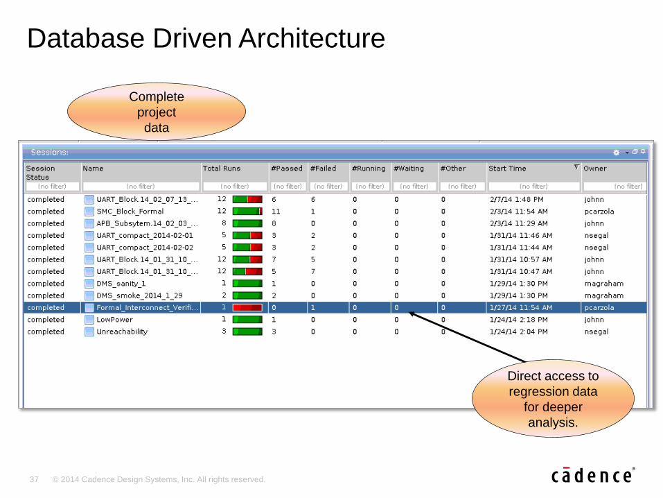
Database Driven Architecture
Complete
project
data
Direct access to
regression data
for deeper
analysis.

38 © 2014 Cadence Design Systems, Inc. All rights reserved.
• Analysis, exclusion and reporting
• Top level verification plan down to low level bin/line/toggle level analysis– Historically split between
multiple tools (spreadsheet, scripts, single run coverage analysis tools)
• Single environment for ALL metric analysis– The right data at the right time
– Low latency access (seconds, single click)
Requirement - Unified Analysis Environment

39 © 2014 Cadence Design Systems, Inc. All rights reserved.
• Failure analysis complements metric roll up in MDV Cockpit
• Integration and automation with debug is a natural fit
• Push button automated rerun with dumping of debug data
• Tight integration with advanced debug platforms– e.g. Cadence Incisive Debug Analyzer
Requirement - Unified Analysis Environment Includes Failure Triage
40 © 2014 Cadence Design Systems, Inc. All rights reserved.
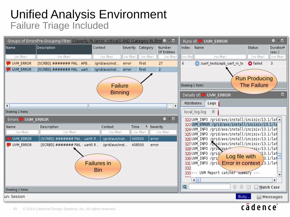
Unified Analysis EnvironmentFailure Triage Included
Failures in
Bin
Run Producing
The Failure
Log file with
Error in context
Failure
Binning

41 © 2014 Cadence Design Systems, Inc. All rights reserved.
React Real-time to Trends
• Utilize “One Touch”real time access toup-to-date results
• Track criticalverification indicators over time for visibility and predictability
• Project Definition– Set of data
– Metrics to track
– Criteria for sample
• Project Tracking and Analysis– Graphical and textual presentation of the metrics results over time
– Persistent storage of trend data in the DB enables team access
42 © 2014 Cadence Design Systems, Inc. All rights reserved.
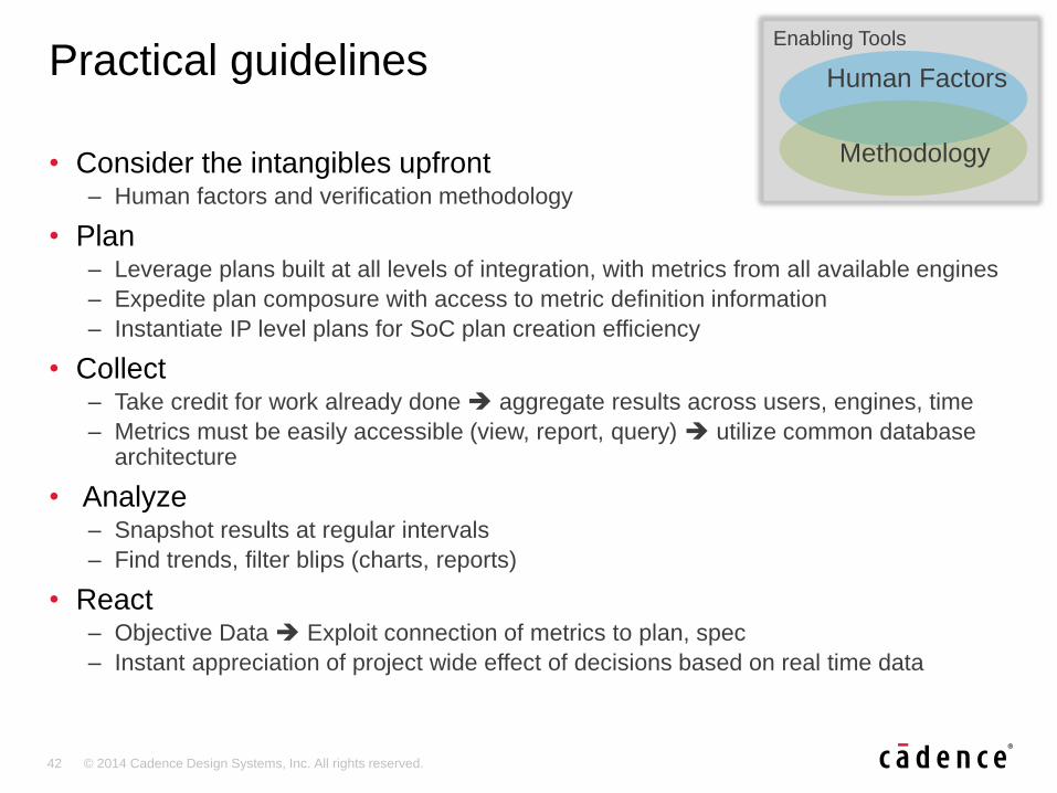
• Consider the intangibles upfront– Human factors and verification methodology
• Plan– Leverage plans built at all levels of integration, with metrics from all available engines
– Expedite plan composure with access to metric definition information
– Instantiate IP level plans for SoC plan creation efficiency
• Collect– Take credit for work already done aggregate results across users, engines, time
– Metrics must be easily accessible (view, report, query) utilize common database architecture
• Analyze– Snapshot results at regular intervals
– Find trends, filter blips (charts, reports)
• React– Objective Data Exploit connection of metrics to plan, spec
– Instant appreciation of project wide effect of decisions based on real time data
Practical guidelines Human Factors
Methodology
Enabling Tools

43 © 2014 Cadence Design Systems, Inc. All rights reserved.
Agenda
Section 1: MDV Methodology IP to SoC Verification
Section 2: MDV Approaches Beyond RTL IP Level
Section 3: Team Based Verification Management
Section 4: MDV In Action
44 © 2014 Cadence Design Systems, Inc. All rights reserved.
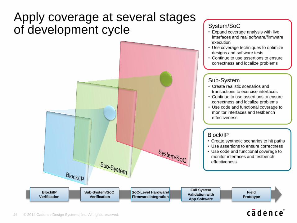
Apply coverage at several stagesof development cycle
Block/IP
Verification
Sub-System/SoC
Verification
SoC-Level Hardware/
Firmware Integration
Field
Prototype
Full System
Validation with
App Software
Block/IP• Create synthetic scenarios to hit paths
• Use assertions to ensure correctness
• Use code and functional coverage to
monitor interfaces and testbench
effectiveness
Sub-System• Create realistic scenarios and
transactions to exercise interfaces
• Continue to use assertions to ensure
correctness and localize problems
• Use code and functional coverage to
monitor interfaces and testbench
effectiveness
System/SoC• Expand coverage analysis with live
interfaces and real software/firmware
execution
• Use coverage techniques to optimize
designs and software tests
• Continue to use assertions to ensure
correctness and localize problems

45 © 2014 Cadence Design Systems, Inc. All rights reserved.
CoverageUse Cases
Use Cases User Explorations (examples)
Applicable
Coverage
Code Functional
SoC
Integration
Verification
• What is the activity between sub-blocks?
• What is the top level activity – perhaps 1 or 2 levels?
Localized and
Full-design focus• How can I run detailed coverage analysis into specific area of interest?
• How do I achieve 100% coverage?
Verify Modes
of Operation
• Are two processing units simultaneously active? Were interfaces active
simultaneously? Was interrupt issued when CPU transfers data to
GPU?
• How do I correlate coverage to design features that I’m testing and
measure progress against my overall verification plan?
Design
Optimization• How is this buffer being used? Undersized? Oversized?
• What is the latency on this operation? Average? Max?
Improving
Hardware
Coverage of
Software Tests
• How much of hardware is being exercised by software tests?
• Should I improve my software tests to achieve higher coverage?
Use Cases User Explorations (examples)
Applicable
Coverage
Code Functional
SoC
Integration
Verification
• What is the activity between sub-blocks?
• What is the top level activity – perhaps 1 or 2 levels?
Use Cases User Explorations (examples)
Applicable
Coverage
Code Functional
SoC
Integration
Verification
• What is the activity between sub-blocks?
• What is the top level activity – perhaps 1 or 2 levels?
Localized and
Full-design focus• How can I run detailed coverage analysis into specific area of interest?
• How do I achieve 100% coverage?
Verify Modes
of Operation
• Are two processing units simultaneously active? Were interfaces active
simultaneously? Was interrupt issued when CPU transfers data to
GPU?
• How do I correlate coverage to design features that I’m testing and
measure progress against my overall verification plan?
Use Cases User Explorations (examples)
Applicable
Coverage
Code Functional
SoC
Integration
Verification
• What is the activity between sub-blocks?
• What is the top level activity—perhaps 1 or 2 levels?
Localized and
Full-design focus• How can I run detailed coverage analysis into specific area of interest?
• How do I achieve 100% coverage?
Verify Modes
of Operation
• Are two processing units simultaneously active? Were interfaces active
simultaneously? Was interrupt issued when CPU transfers data to
GPU?
• How do I correlate coverage to design features that I’m testing and
measure progress against my overall verification plan?
Design
Optimization• How is this buffer being used? Undersized? Oversized?
• What is the latency on this operation? Average? Max?

46 © 2014 Cadence Design Systems, Inc. All rights reserved.
Code coverage problem statement
• Traditional code coverage use model is difficult– Add an option and get overwhelmed with data
– System verification engineers aren’t going to understand coverage data at low levels
of the design
– Even if they did, very difficult to influence low level logic from system level tests
• Solution?– Focus on actionable data
system
CPU 1 CPU 2 GPU mem network
What is this
signal or
code?
How can I
control from
top-level
testbench?

47 © 2014 Cadence Design Systems, Inc. All rights reserved.
Integration verification
• Cover connectivity between top-level modules– That’s what’s new and untested
– Lower level blocks have been verified at the block level
– Understandable and actionable by system verification engineers
– Typically would use toggle coverage on ports of top-level blocks
– Block coverage not as interesting at higher levels limited RTL– Might have small pieces of new system-level controller logic
Code Functional
system
CPU 1 CPU 2 GPU mem network
Enable Code
Coverage
Disable Code
Coverage
GPU Application (26 MGate)
# hier levels # toggle signals
1 3,000
2 101,000
# hier levels # toggle signals
3 717,000
5 14,400,000
all 27,400,000

48 © 2014 Cadence Design Systems, Inc. All rights reserved.
Low-speed peripheral
subsystem
Localized focus—go deep
• Focus on a particular region of the design– Manage “amount of coverage data”
– New or lesser tested area
– Specific concerns with coverage in an area
– Access to designers
– Can merge multiple regional coverage databases into a complete view
Application Specific Components
SoC Interconnect Fabric
ARM CPU Subsystem
3D
Graphics
CoreModem
High speed, wired interface peripherals
Other
peripherals
GPIO
Application
Accelerators
…
AES
…
Flash
A7
L2 cache
A7
Cache Coherent Fabric
A15
L2 cache
A15
Display
PMU
MPI
UART
INTC
I2C
Timer
JTAG SPI
HDMI
SATA
MIPI
WLAN
LTE
PHY
DDR3
Ctrlr
PHY
PCIe
Gen 2,3
PHY
USB 3.0
3.0
PHY
2.0
PHY
Third-party
IP block
Re-used,
well tested
peripheral
blocks
Newly designed
or modified
blocks for this
project
New, complex
interconnect
Code Functional

49 © 2014 Cadence Design Systems, Inc. All rights reserved.
V
C
System-level functional coverage example
Block
1
Block
2
Block
3
V
C
Mem
FC
FC
Block-level verification
focus
Sub-system, system-level
verification focus
Testbench
V
C
V
C
FCFC
Testbench
V
C
V
C
FCFC
Testbench
V
C
V
C
FCFC
Block
1
Block
2
Block
2
Block
3

50 © 2014 Cadence Design Systems, Inc. All rights reserved.
V
C
V
C
Mem
FC
FC
Block
1
Block
2
Block
2
Block
3
• Can maintain some monitors for coverage from the subsystem level
• Fundamentally, asking different questions at the system level– Concerned with interactions
between subsystems
– Implies a system level test plan tied to design spec
• Verifying modes of operation– Were these two processing units
active simultaneously?
– Were these interfaces active simultaneously?
– Have I received an interrupt when the CPU is transferring data to the GPU?
Verify modes of operation
FC
FC
New!
Reuse
M
O
N
FC
Code Functional

51 © 2014 Cadence Design Systems, Inc. All rights reserved.
V
C
V
C
Mem
FC
FC
Block
1
Block
2
Block
2
Block
3
Verify modes of operation
FC
FC
M
O
N
FC
Code Functional

52 © 2014 Cadence Design Systems, Inc. All rights reserved.
V
C
V
C
Mem
FC
FC
Block
1
Block
2
Block
2
Block
3
FC
FC
M
O
N
FC
• Investigate performance in real-world scenarios– What is the average utilization of
the FIFO?
– If low, can we reduce the FIFO size?
– If high, can we expand the FIFO orcan we optimize the application
software?
• You may have seen cases where designers put in special counters and instrumentation– Covergroups and cover properties
are a very easy way to instrument, plus there are standard tools for merging, reporting and analyzing results
Design optimization
0
10
20
30
40
50
60
70
80
90
100
FIFO with Low Utilization
0
10
20
30
40
50
60
70
80
90
100
FIFO with High Utilization
covergroup cg @(posedge clk);coverpoint count iff (wr_en);
endgroup
Optimize
Code Functional
Increase
Size?

53 © 2014 Cadence Design Systems, Inc. All rights reserved.
Proc
Customer’s Application Specific Components
SoC Interconnect Fabric
ARM CPU Subsystem
3D
Graphi
cs
Core
Mod
em
High speed, wired interface peripherals
DD
R3
Ctrll
er
PH
Y
Other peripherals
SAT
A
MIPI
HDM
I
WLA
N
LTELow-speed peripheral
subsystem
Low speed peripherals
PM
UMIP
IJTA
G
INT
C
I2C
Tim
er
SPI
GPI
O
Display
UA
RT
Applicati
on
Accelera
tors…
AE
S
…
A15
L2 cache
USB3.
0
3
.
0P
H
Y
2
.
0P
H
Y
PCIe
Gen
2,3
PHY
Fla
sh
PH
Y
A15 A7
L2 cache
A7
Cache Coherent Fabric
Coverage Enabled
• Software-validation process often independent of hardware-verification process
• How well is the software exercising the hardware?
• Get a sense of “coverage” of the software through enabling hardware coverage during the running of software tests
Operating Systems (OS)
Drivers
Applications
Middleware
Firmware/HAL
Code Functional
?
Improving hardware coverage of software tests

54 © 2014 Cadence Design Systems, Inc. All rights reserved.
• Software-validation process often independent of hardware-verification process
• How well is the software exercising the hardware?
• Get a sense of “coverage” of the software through enabling hardware coverage during the running of software tests
Proc
Customer’s Application Specific Components
SoC Interconnect Fabric
ARM CPU Subsystem
3D
Graphi
cs
Core
Mod
em
High speed, wired interface peripherals
DD
R3
Ctrll
er
PH
Y
Other peripherals
SAT
A
MIPI
HDM
I
WLA
N
LTELow-speed peripheral
subsystem
Low speed peripherals
PM
UMIP
IJTA
G
INT
C
I2C
Tim
er
SPI
GPI
O
Display
UA
RT
Applicati
on
Accelera
tors…
AE
S
…
A15
L2 cache
USB3.
0
3
.
0P
H
Y
2
.
0P
H
Y
PCIe
Gen
2,3
PHY
Fla
sh
PH
Y
A15 A7
L2 cache
A7
Cache Coherent Fabric
Operating Systems (OS)
Drivers
Applications
Middleware
Firmware/HAL
Code Functional
Block Coverage Enabled
0%
20%
40%
60%
80%
100%
Coverage
Coverage
Improving hardware coverage of software tests

55 © 2014 Cadence Design Systems, Inc. All rights reserved.
DEMONSTRATION

56 © 2014 Cadence Design Systems, Inc. All rights reserved.
MDV Tutorial Summary

57 © 2014 Cadence Design Systems, Inc. All rights reserved.
SoC MDV – Multi User, Multi Engine, Multi MetricEnvironment pulling together contributions from all users, engines, and metrics

58 © 2014 Cadence Design Systems, Inc. All rights reserved.
SoC MDV – Multi Engine, Multi Metric PlanExecutable verification plan that can link to all necessary engines and metrics
59 © 2014 Cadence Design Systems, Inc. All rights reserved.
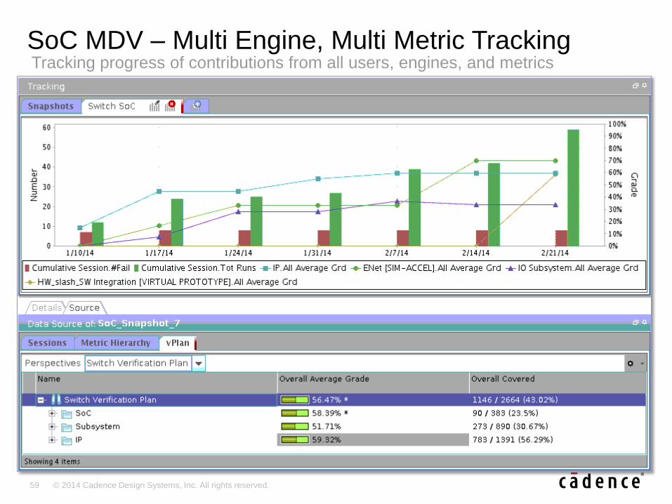
SoC MDV – Multi Engine, Multi Metric TrackingTracking progress of contributions from all users, engines, and metrics

60 © 2014 Cadence Design Systems, Inc. All rights reserved.
• MDV has been proved to improve predictability and productivity at IP to Sub-System Levels
• Today you have learned how MDV can be expanded using vManager to operate across specialized verification engines
• Additionally you have learned how MDV can be used thru to SOC level verification.
• MDV at SOC is new and emerging, and Cadence is committed to codify and optimize this for the industry, just like we did with UVM from eRM at IP levels
• Thank you for your participation today. You can learn more about the vManager Solution and MDV on the Cadence website – www.cadence.com
The How To’s of Metric Driven Verification to Maximize Productivity

61 © 2012 Cadence Design Systems, Inc. All rights reserved.

Questions ?
© Accellera Systems Initiative 62