Embed Size (px)
Citation preview
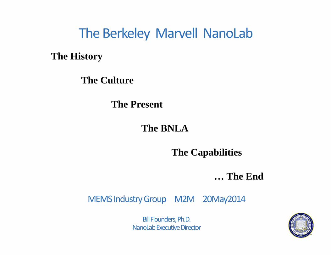
The Berkeley Marvell NanoLabThe History
The Culture
The Present
The BNLA
The Capabilities
… The End
MEMS Industry Group M2M 20May2014
Bill Flounders, Ph.D.NanoLabExecutive Director
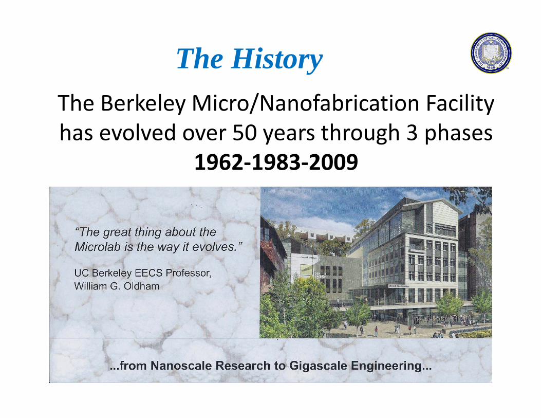
The HistoryThe Berkeley Micro/Nanofabrication Facilityhas evolved over 50 years through 3 phases
1962‐1983‐2009
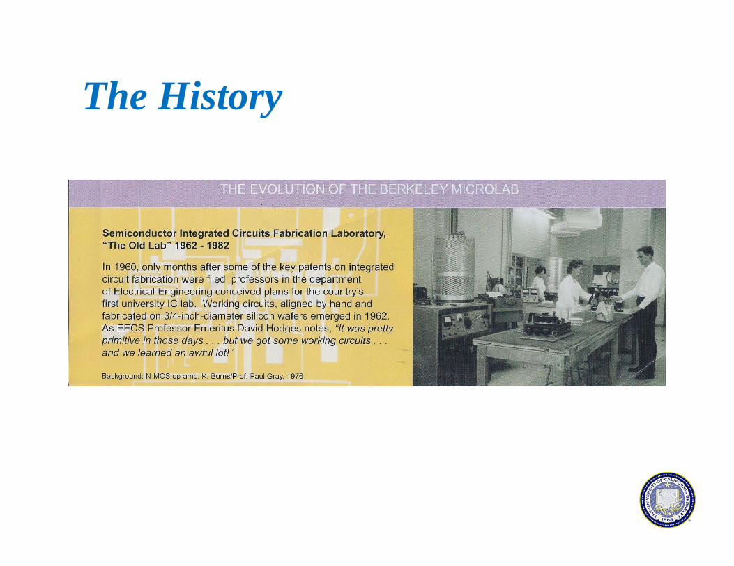
The History
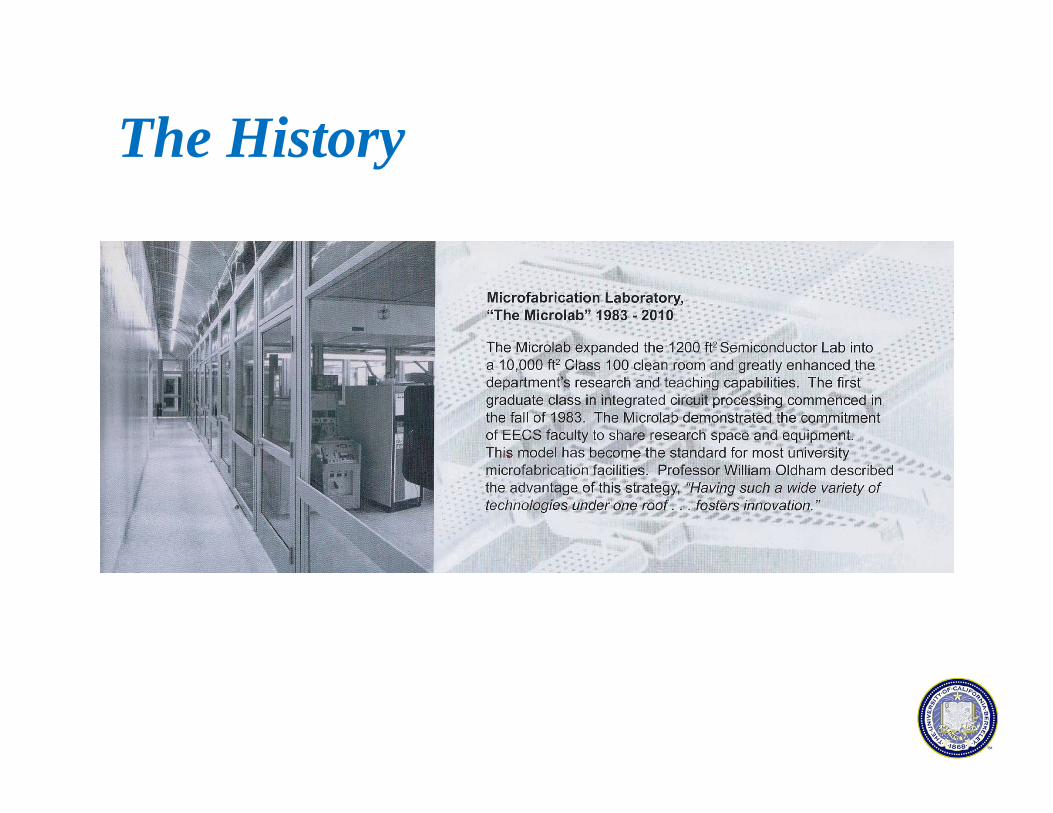
The History
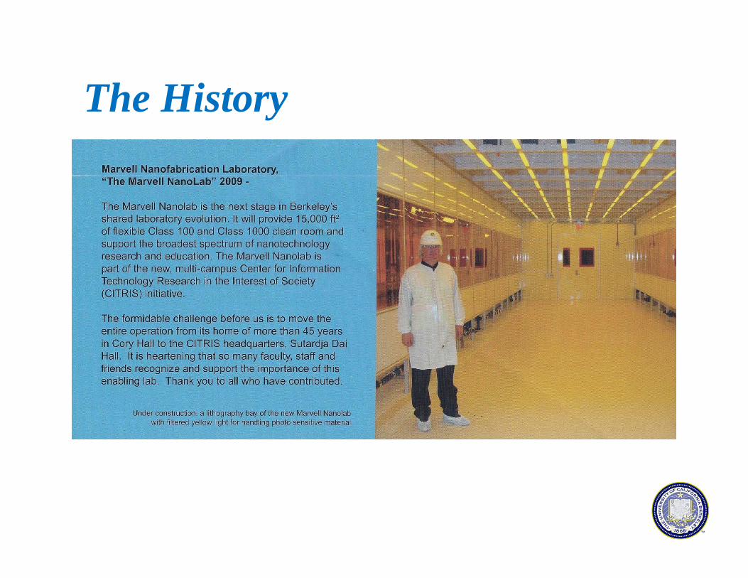
The History
The Culture A self supporting operation
~ $5 M annual operating budget >200 grants billed, enables >$40M in research contracts~20 company members providing ~1/3 revenue
Faculty DriveNew equipment, custom modifications, and new materials are driven by faculty research programs and industry collaborations
Lab Management and Staff Steer Facility Management, Utility Support, Resource CoordinationEquipment Maintenance, Process Development
The Culture The NanoLab is a research community
researchers are considered members not usersacademic research is the priority missionit is a highly diverse lab environment, Si, III-V, glass, plastic
Process and Equipment Staff are Community LeadersStaff provide information, guidance and equipment/process development. They don’t do your work for you
Every tool has a primary and a back up equipment and process engineer.Every tool has a standard process. Equipment considered up when results of the standard process are within spec
Process staff execute standard process after major repair andaccording to periodic schedule called Quality Monitoring
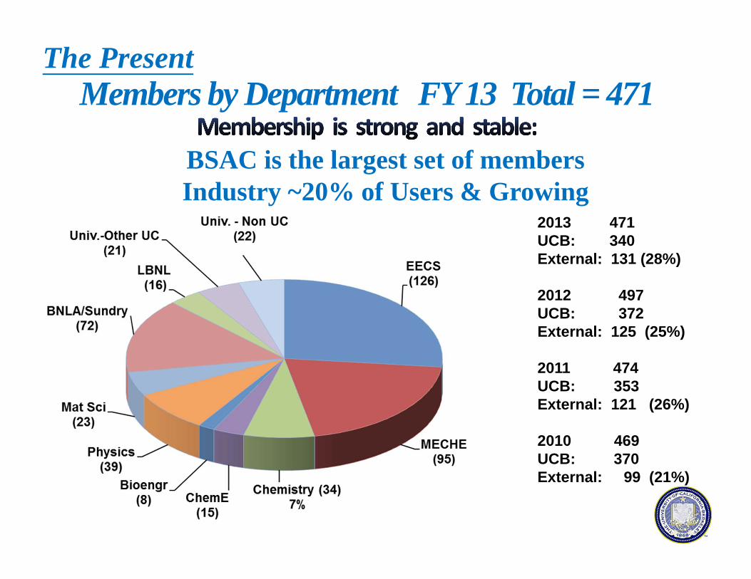
Members by Department FY 13 Total = 471
2013 471UCB: 340External: 131 (28%)
2012 497UCB: 372External: 125 (25%)
2011 474 UCB: 353External: 121 (26%)
2010 469UCB: 370 External: 99 (21%)
BSAC is the largest set of membersIndustry ~20% of Users & Growing
The Present
The Present
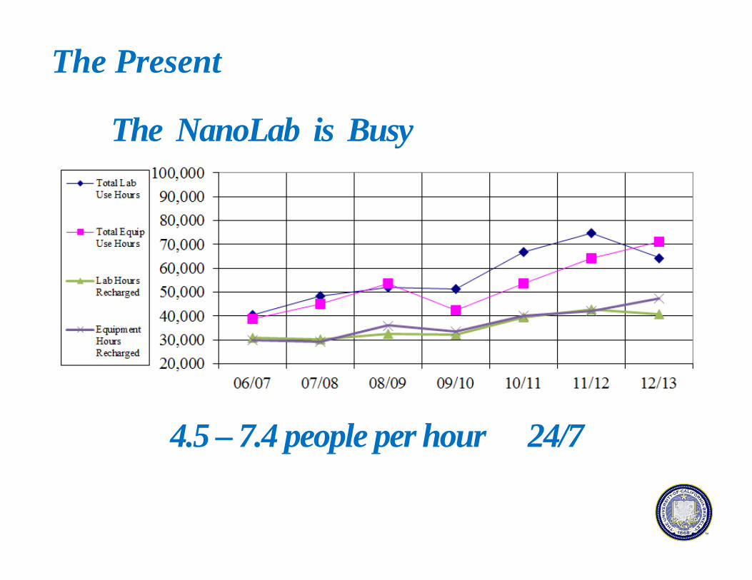
The NanoLab is Busy
4.5 – 7.4 people per hour 24/7
Industry Affiliates WelcomeBNLA Program Enables Company Access
Companies request access to the NanoLab for experimental work, subject to recharge fees. Primarily but not exclusively start ups.
Director reviews Company’s proposed use and verifies it does not conflict with “academic research priorities”
Companies pay annual membership fee + equipment recharge
Commercial researchers are and are viewed as contributing members of the laboratory
The BNLA
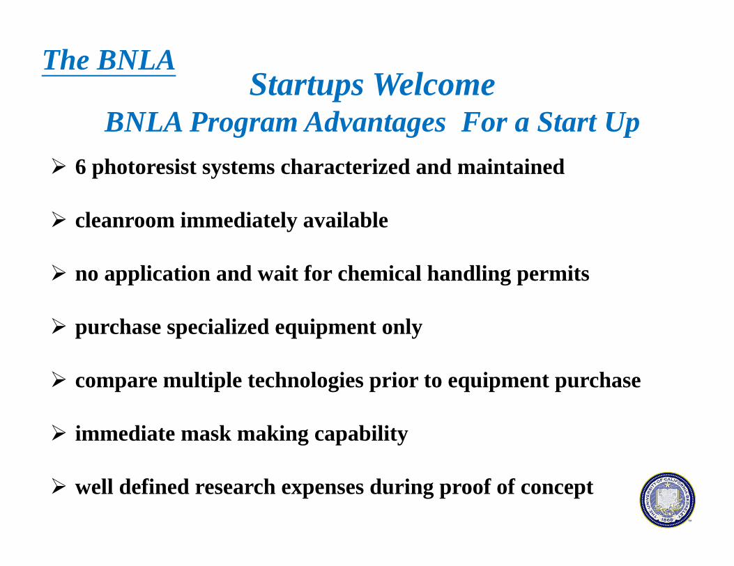
Startups WelcomeBNLA Program Advantages For a Start Up
6 photoresist systems characterized and maintained
cleanroom immediately available
no application and wait for chemical handling permits
purchase specialized equipment only
compare multiple technologies prior to equipment purchase
immediate mask making capability
well defined research expenses during proof of concept
The BNLA
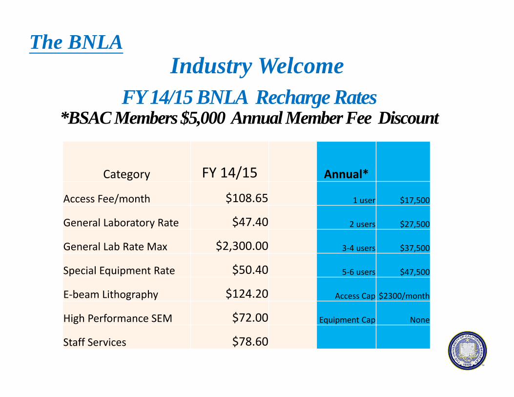
Industry WelcomeFY 14/15 BNLA Recharge Rates
*BSAC Members $5,000 Annual Member Fee Discount
Category FY 14/15 Annual*
Access Fee/month $108.65 1 user $17,500
General Laboratory Rate $47.40 2 users $27,500
General Lab Rate Max $2,300.00 3‐4 users $37,500
Special Equipment Rate $50.40 5‐6 users $47,500
E‐beam Lithography $124.20 Access Cap $2300/month
High Performance SEM $72.00 Equipment Cap None
Staff Services $78.60
The BNLA
The Capabilities
The Microlab has had a “Baseline Monitor” effort for more than 10 years. Grew out of the CMOS Baseline
Select processes are run by process staff on a regular basis and results are posted at NanoLab website
This effort has been expanded to include more equipment, track etch selectivity, include etch images
Selectivity monitoring requires patterning; images require SEM time.
Staff Supported Quality Monitoring Program
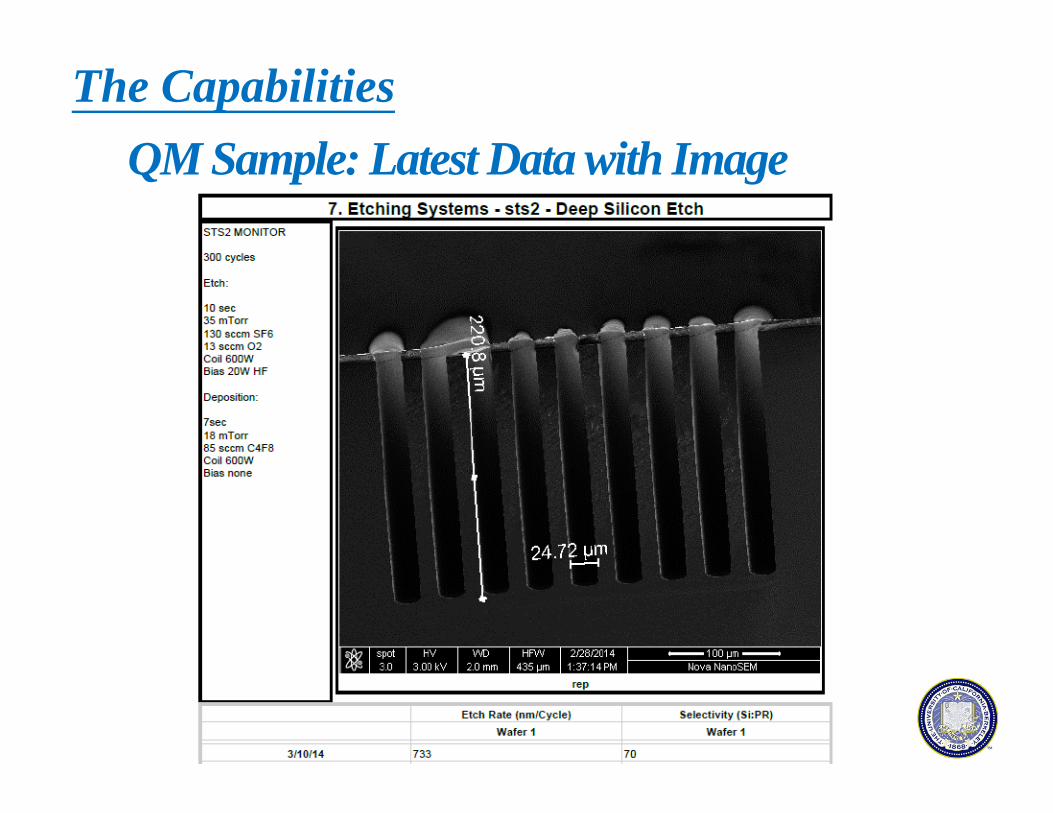
The CapabilitiesQM Sample: Latest Data with Image
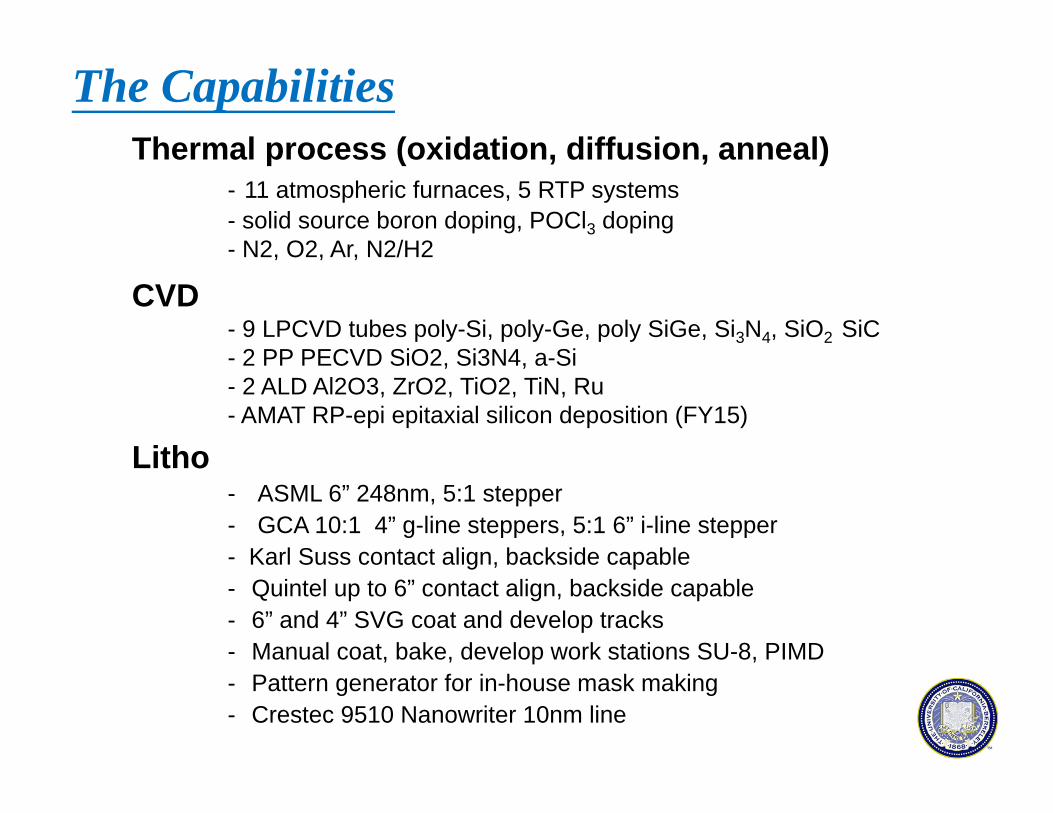
The CapabilitiesThermal process (oxidation, diffusion, anneal)
- 11 atmospheric furnaces, 5 RTP systems- solid source boron doping, POCl3 doping- N2, O2, Ar, N2/H2
CVD- 9 LPCVD tubes poly-Si, poly-Ge, poly SiGe, Si3N4, SiO2 SiC- 2 PP PECVD SiO2, Si3N4, a-Si- 2 ALD Al2O3, ZrO2, TiO2, TiN, Ru- AMAT RP-epi epitaxial silicon deposition (FY15)
Litho- ASML 6” 248nm, 5:1 stepper- GCA 10:1 4” g-line steppers, 5:1 6” i-line stepper- Karl Suss contact align, backside capable- Quintel up to 6” contact align, backside capable- 6” and 4” SVG coat and develop tracks- Manual coat, bake, develop work stations SU-8, PIMD- Pattern generator for in-house mask making- Crestec 9510 Nanowriter 10nm line
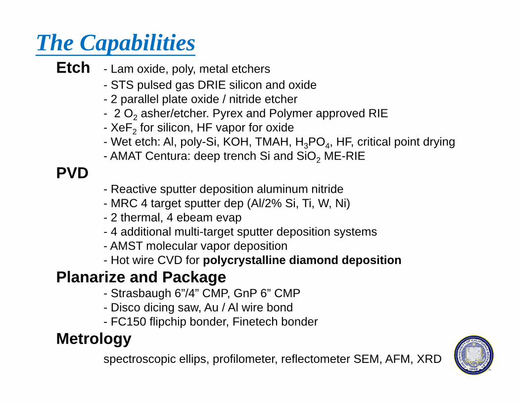
The CapabilitiesEtch - Lam oxide, poly, metal etchers
- STS pulsed gas DRIE silicon and oxide- 2 parallel plate oxide / nitride etcher- 2 O2 asher/etcher. Pyrex and Polymer approved RIE- XeF2 for silicon, HF vapor for oxide - Wet etch: Al, poly-Si, KOH, TMAH, H3PO4, HF, critical point drying- AMAT Centura: deep trench Si and SiO2 ME-RIE
PVD- Reactive sputter deposition aluminum nitride- MRC 4 target sputter dep (Al/2% Si, Ti, W, Ni)- 2 thermal, 4 ebeam evap- 4 additional multi-target sputter deposition systems- AMST molecular vapor deposition - Hot wire CVD for polycrystalline diamond deposition
Planarize and Package- Strasbaugh 6”/4” CMP, GnP 6” CMP- Disco dicing saw, Au / Al wire bond- FC150 flipchip bonder, Finetech bonder
Metrology spectroscopic ellips, profilometer, reflectometer SEM, AFM, XRD
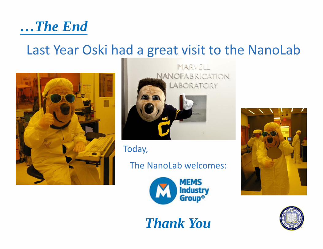
Last Year Oski had a great visit to the NanoLab
…The End
Today,
The NanoLab welcomes:
Thank You