Embed Size (px)
Citation preview
1
The HADES RPC Frontend Readout System
D. Belver 4, J. A. Garzon 4, A. Gil 2, D. Gonzalez 4,J. S. Lange 3, J. Marin 1, N. Montes 4, P. Skott 3,
M. Traxler 3, W. Koenig 3
1 CIEMAT, Madrid2 IFIC, Valencia
3 GSI, Darmstadt4 Univ. Santiago de Compostela
1st FAIR-FEE Workshop, GSI Darmstadt, 11-13.10.2005
J. S. Lange (GSI) HADES RPC Frontend FAIR FEE Workshop, 11.-13.10.2005 2
Content
• The Daughterboard (DB)
• 2nd iteration (STEP2)• 3rd iteration (STEP3)• 4th iteration (STEP4) – pre-final
• The Motherboard (MB)
• The Power Supply Board (RPS)
• Test results from 2 Santiago tests and 2 LIP/Coimbra tests
• Note: this talk covers everything in front of the TDC board (see talks by K. Korcyl, M. Palka)
J. S. Lange (GSI) HADES RPC Frontend FAIR FEE Workshop, 11.-13.10.2005 3
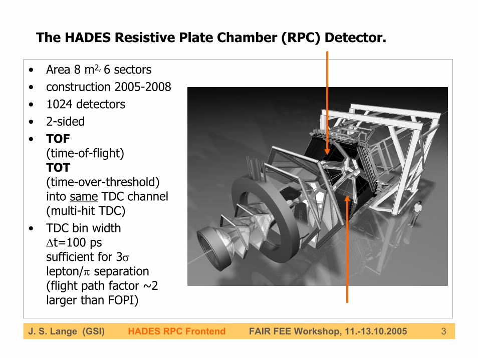
The HADES Resistive Plate Chamber (RPC) Detector.
• Area 8 m2, 6 sectors• construction 2005-2008• 1024 detectors• 2-sided• TOF
(time-of-flight)TOT(time-over-threshold)into same TDC channel(multi-hit TDC)
• TDC bin width∆t=100 pssufficient for 3σlepton/π separation(flight path factor ~2larger than FOPI)
J. S. Lange (GSI) HADES RPC Frontend FAIR FEE Workshop, 11.-13.10.2005 4
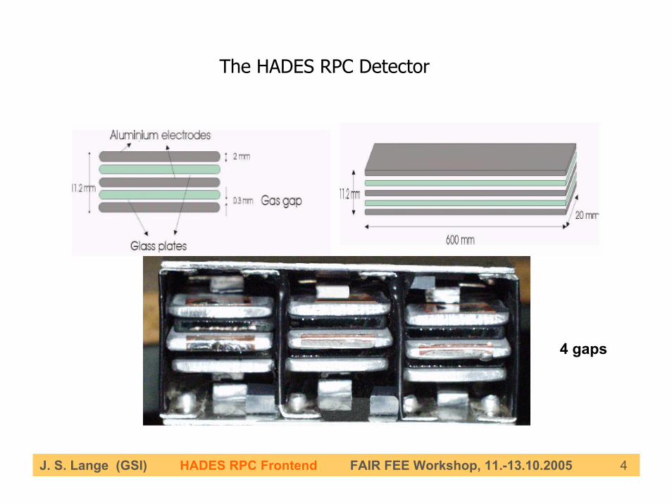
The HADES RPC Detector
4 gaps
J. S. Lange (GSI) HADES RPC Frontend FAIR FEE Workshop, 11.-13.10.2005 5
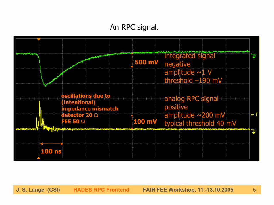
An RPC signal.
integrated signal negativeamplitude ~1 Vthreshold –190 mV
analog RPC signalpositiveamplitude ~200 mVtypical threshold 40 mV
oscillations due to(intentional) impedance mismatch detector 20 ΩFEE 50 Ω
100 ns
100 mV
500 mV
J. S. Lange (GSI) HADES RPC Frontend FAIR FEE Workshop, 11.-13.10.2005 6
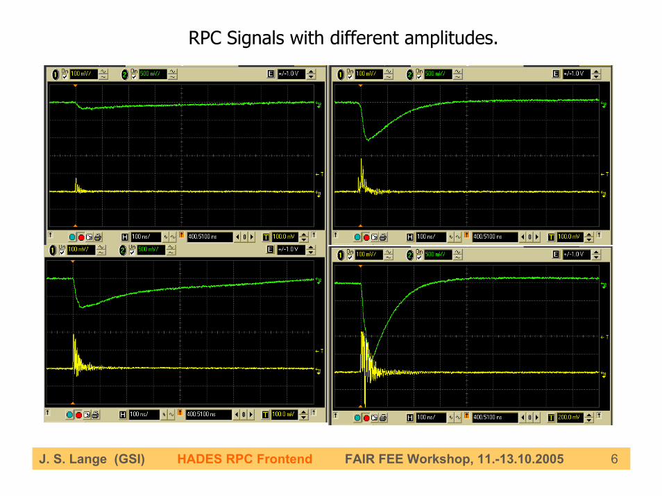
RPC Signals with different amplitudes.
J. S. Lange (GSI) HADES RPC Frontend FAIR FEE Workshop, 11.-13.10.2005 7
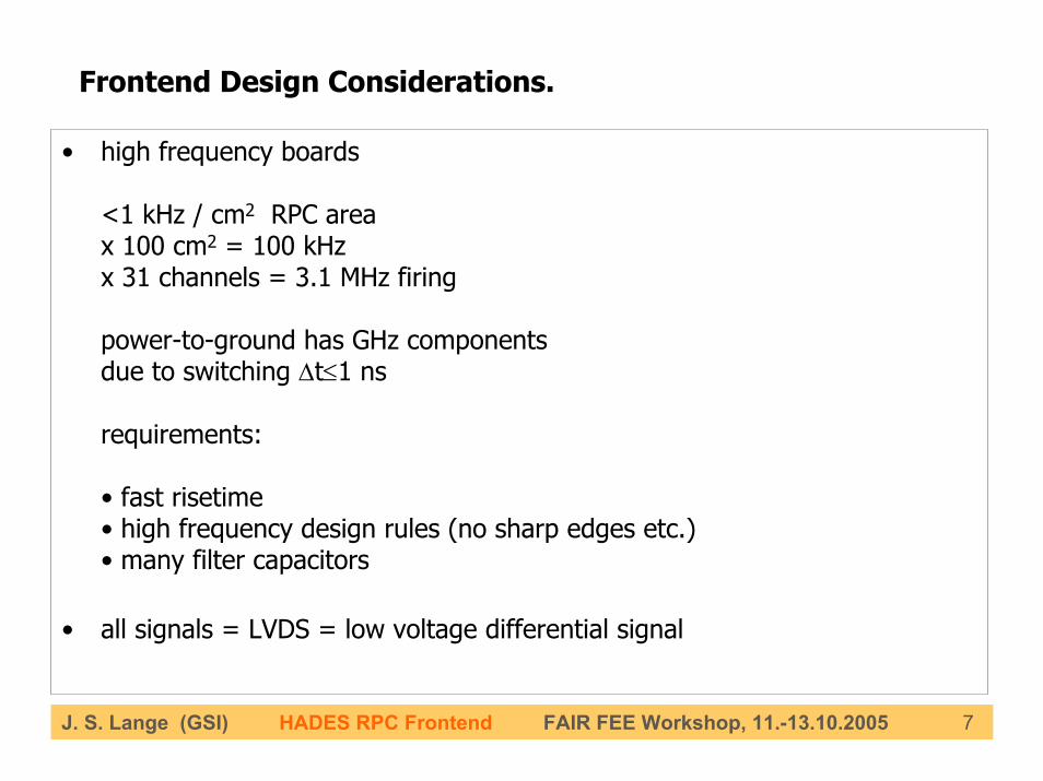
Frontend Design Considerations.
• high frequency boards
<1 kHz / cm2 RPC areax 100 cm2 = 100 kHzx 31 channels = 3.1 MHz firing
power-to-ground has GHz components due to switching ∆t≤1 ns
requirements:
• fast risetime• high frequency design rules (no sharp edges etc.)• many filter capacitors
• all signals = LVDS = low voltage differential signal
J. S. Lange (GSI) HADES RPC Frontend FAIR FEE Workshop, 11.-13.10.2005 8
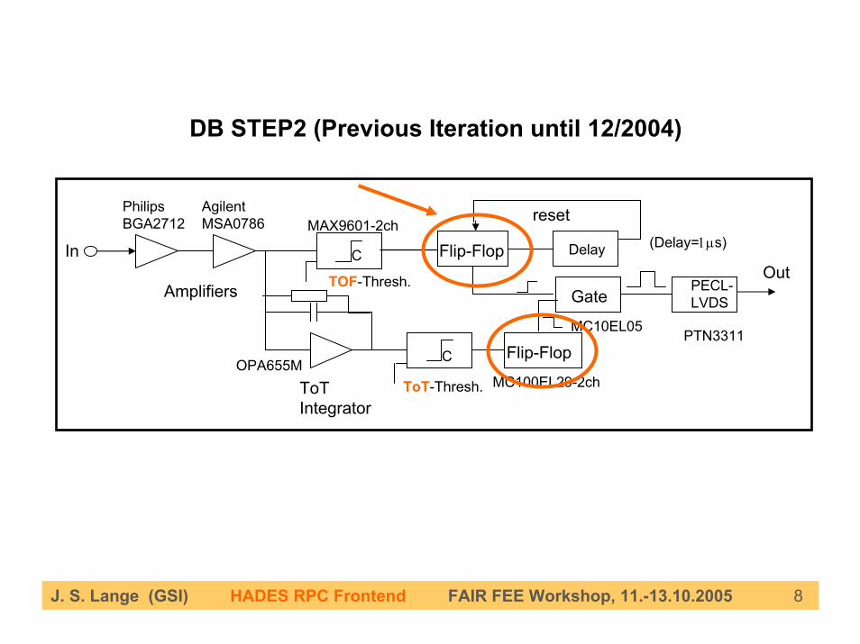
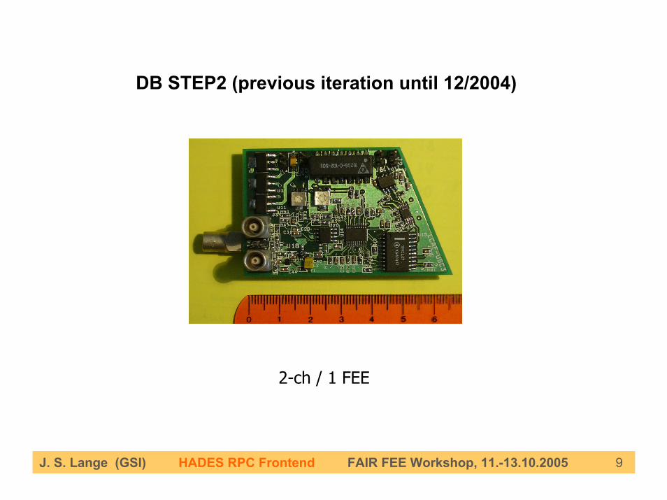
DB STEP2 (Previous Iteration until 12/2004)
C
C
ToTIntegrator
Amplifiers
Flip-Flop
Flip-Flop
Gate
reset
PECL-LVDS
TOF-Thresh.
ToT-Thresh.
InOut
Delay
OPA655M
(Delay=1µs)
PhilipsBGA2712
Agilent MSA0786 MAX9601-2ch
MC100EL29-2ch
MC10EL05 PTN3311
J. S. Lange (GSI) HADES RPC Frontend FAIR FEE Workshop, 11.-13.10.2005 9
DB STEP2 (previous iteration until 12/2004)
2-ch / 1 FEE
J. S. Lange (GSI) HADES RPC Frontend FAIR FEE Workshop, 11.-13.10.2005 10
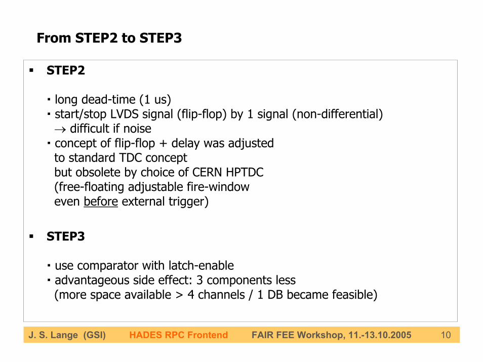
From STEP2 to STEP3
STEP2
long dead-time (1 us)start/stop LVDS signal (flip-flop) by 1 signal (non-differential)→ difficult if noise concept of flip-flop + delay was adjusted to standard TDC conceptbut obsolete by choice of CERN HPTDC (free-floating adjustable fire-window even before external trigger)
STEP3
use comparator with latch-enableadvantageous side effect: 3 components less (more space available > 4 channels / 1 DB became feasible)
J. S. Lange (GSI) HADES RPC Frontend FAIR FEE Workshop, 11.-13.10.2005 11
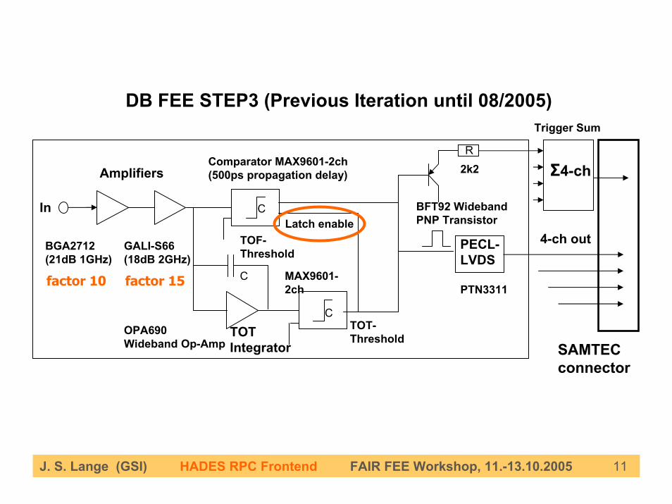
DB FEE STEP3 (Previous Iteration until 08/2005) Trigger Sum
C
C
TOTIntegrator
Amplifiers
PECL-LVDS
TOF-Threshold
TOT-Threshold
In
OPA690 Wideband Op-Amp
BGA2712(21dB 1GHz)
GALI-S66 (18dB 2GHz)
Comparator MAX9601-2ch (500ps propagation delay)
PTN3311C
Latch enable
MAX9601-2ch
R
2k2
4-ch out
Σ4-ch
BFT92 Wideband PNP Transistor
factor 10 factor 15
SAMTECconnector
J. S. Lange (GSI) HADES RPC Frontend FAIR FEE Workshop, 11.-13.10.2005 12
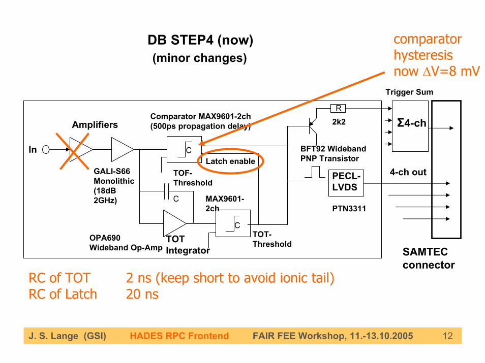
DB STEP4 (now)(minor changes)
4-ch out
C
C
TOTIntegrator
Amplifiers
PECL-LVDS
TOF-Threshold
TOT-Threshold
In
OPA690 Wideband Op-Amp
GALI-S66 Monolithic(18dB 2GHz)
Comparator MAX9601-2ch (500ps propagation delay)
PTN3311C
Latch enable
MAX9601-2ch
R
2k2
Trigger Sum
Σ4-ch
SAMTECconnector
BFT92 Wideband PNP Transistor
comparatorhysteresisnow ∆V=8 mV
RC of TOT 2 ns (keep short to avoid ionic tail)RC of Latch 20 ns
J. S. Lange (GSI) HADES RPC Frontend FAIR FEE Workshop, 11.-13.10.2005 13
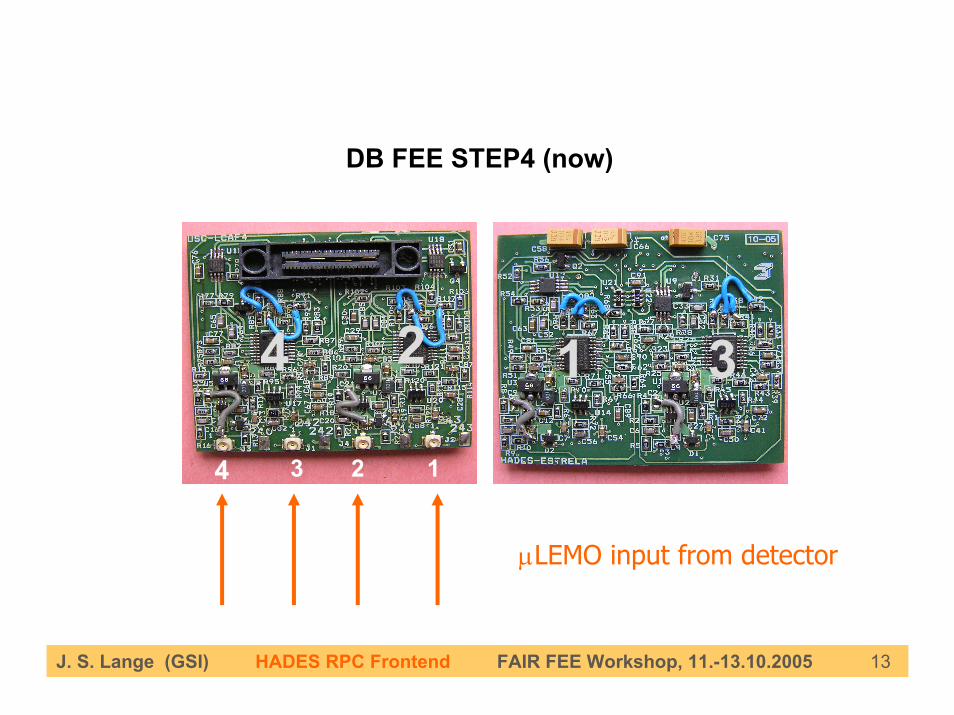
DB FEE STEP4 (now)
4 3 2 1
1 3 2 4
14 32
µLEMO input from detector
J. S. Lange (GSI) HADES RPC Frontend FAIR FEE Workshop, 11.-13.10.2005 14
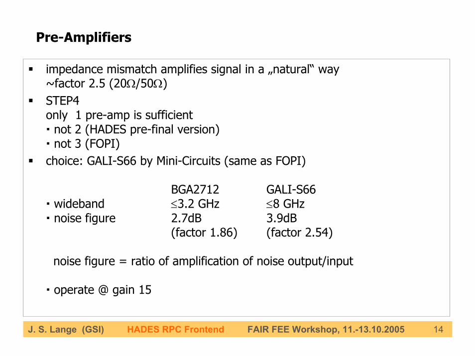
Pre-Amplifiers
impedance mismatch amplifies signal in a „natural“ way ~factor 2.5 (20Ω/50Ω)STEP4 only 1 pre-amp is sufficient
not 2 (HADES pre-final version)not 3 (FOPI)
choice: GALI-S66 by Mini-Circuits (same as FOPI)
BGA2712 GALI-S66wideband ≤3.2 GHz ≤8 GHznoise figure 2.7dB 3.9dB
(factor 1.86) (factor 2.54)
noise figure = ratio of amplification of noise output/input
operate @ gain 15
J. S. Lange (GSI) HADES RPC Frontend FAIR FEE Workshop, 11.-13.10.2005 15
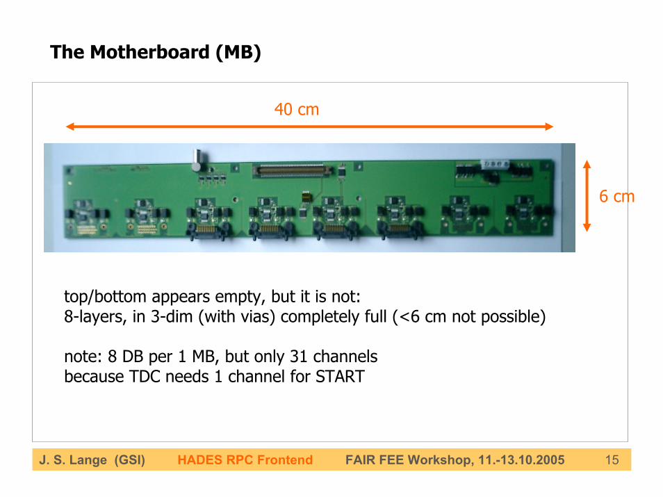
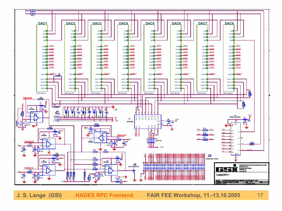
The Motherboard (MB)
top/bottom appears empty, but it is not:8-layers, in 3-dim (with vias) completely full (<6 cm not possible)
note: 8 DB per 1 MB, but only 31 channelsbecause TDC needs 1 channel for START
40 cm
6 cm
J. S. Lange (GSI) HADES RPC Frontend FAIR FEE Workshop, 11.-13.10.2005 16
4 Main Tasks of the MB
• 1. supply stable voltage to DB+5 V+3.3 V-5 V
• 2. get logical signals (TOF and TOT) from 8 daughterboardsand concentrate to 1 connector(then twisted pair HITACHI cable to TDC board)
• 3. generate multiplicity signal for trigger• 4. set thresholds on DB
for TOF and TOTuse programmable DAC chips
• And a few minor tasks:multiplex/fan-out test signals 1→16 (from TDC board), invert polarity of TOT thresholds,LVDS repeaters etc.
J. S. Lange (GSI) HADES RPC Frontend FAIR FEE Workshop, 11.-13.10.2005 17
Title
J. S. Lange (GSI) HADES RPC Frontend FAIR FEE Workshop, 11.-13.10.2005 18
Title
J. S. Lange (GSI) HADES RPC Frontend FAIR FEE Workshop, 11.-13.10.2005 19
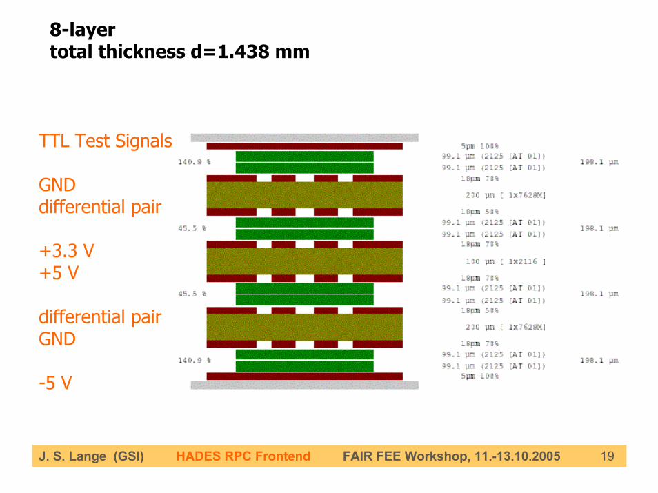
8-layertotal thickness d=1.438 mm
TTL Test Signals
GNDdifferential pair
+3.3 V+5 V
differential pairGND
-5 V
J. S. Lange (GSI) HADES RPC Frontend FAIR FEE Workshop, 11.-13.10.2005 20
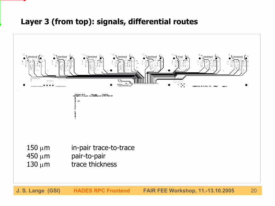
Layer 3 (from top): signals, differential routes
150 µm in-pair trace-to-trace450 µm pair-to-pair 130 µm trace thickness
J. S. Lange (GSI) HADES RPC Frontend FAIR FEE Workshop, 11.-13.10.2005 21
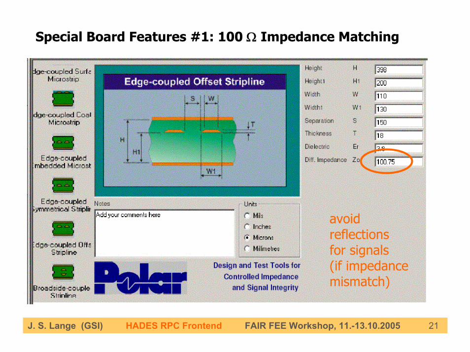
Special Board Features #1: 100 Ω Impedance Matching
avoid reflectionsfor signals(if impedancemismatch)
J. S. Lange (GSI) HADES RPC Frontend FAIR FEE Workshop, 11.-13.10.2005 22
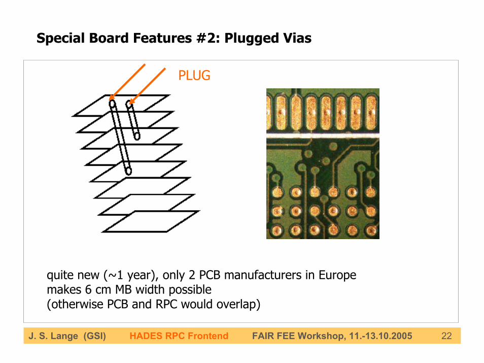
Special Board Features #2: Plugged Vias
PLUG
quite new (~1 year), only 2 PCB manufacturers in Europemakes 6 cm MB width possible(otherwise PCB and RPC would overlap)
J. S. Lange (GSI) HADES RPC Frontend FAIR FEE Workshop, 11.-13.10.2005 23
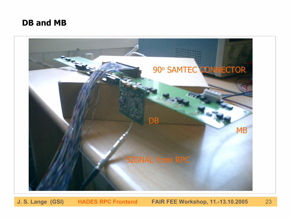
DB and MB
SIGNAL from RPC
90o SAMTEC CONNECTOR
MBDB
J. S. Lange (GSI) HADES RPC Frontend FAIR FEE Workshop, 11.-13.10.2005 24
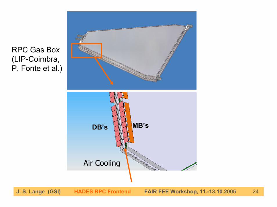
RPC Gas Box(LIP-Coimbra,P. Fonte et al.)
DB’s MB’s
Air Cooling
J. S. Lange (GSI) HADES RPC Frontend FAIR FEE Workshop, 11.-13.10.2005 25
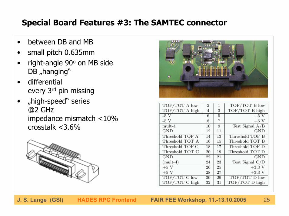
Special Board Features #3: The SAMTEC connector
• between DB and MB• small pitch 0.635mm• right-angle 90o on MB side
DB „hanging“• differential
every 3rd pin missing• „high-speed“ series
@2 GHzimpedance mismatch <10%crosstalk <3.6%
J. S. Lange (GSI) HADES RPC Frontend FAIR FEE Workshop, 11.-13.10.2005 26
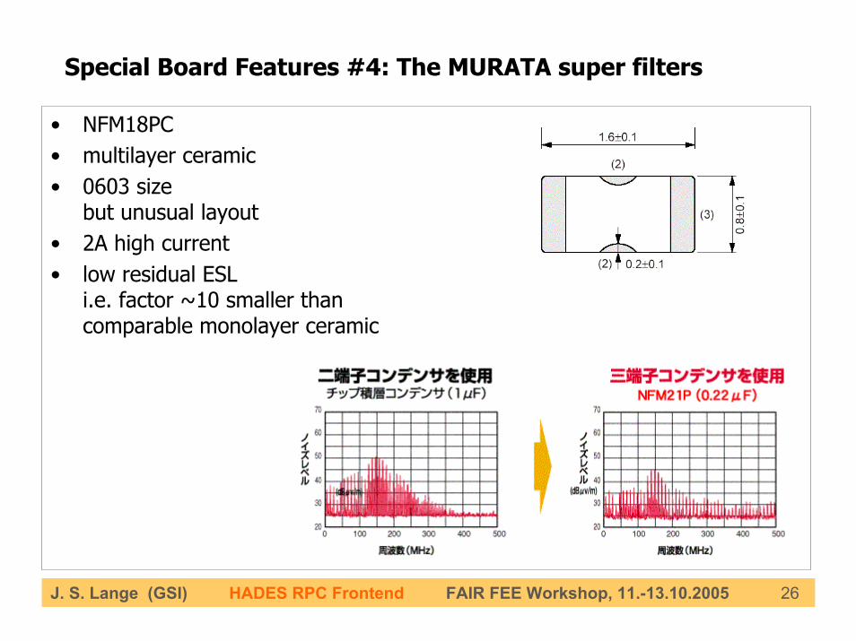
Special Board Features #4: The MURATA super filters
• NFM18PC• multilayer ceramic• 0603 size
but unusual layout • 2A high current• low residual ESL
i.e. factor ~10 smaller than comparable monolayer ceramic
J. S. Lange (GSI) HADES RPC Frontend FAIR FEE Workshop, 11.-13.10.2005 27
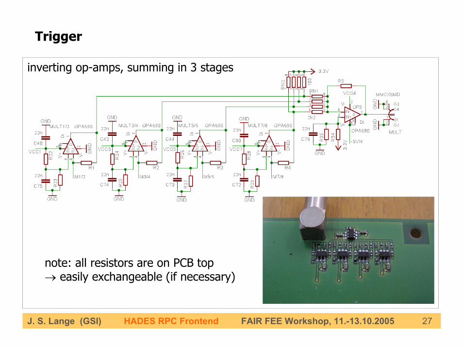
Trigger
inverting op-amps, summing in 3 stages
note: all resistors are on PCB top→ easily exchangeable (if necessary)
J. S. Lange (GSI) HADES RPC Frontend FAIR FEE Workshop, 11.-13.10.2005 28
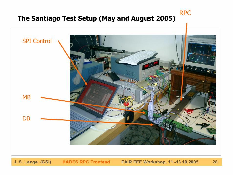
RPCThe Santiago Test Setup (May and August 2005)
SPI Control
MB
DB
J. S. Lange (GSI) HADES RPC Frontend FAIR FEE Workshop, 11.-13.10.2005 29
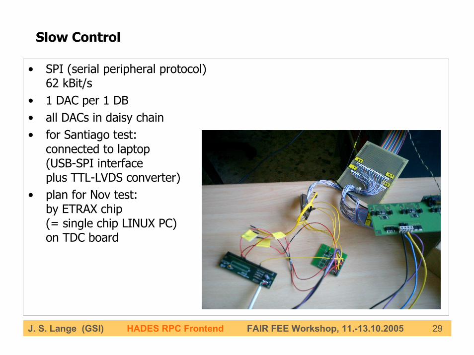
Slow Control
• SPI (serial peripheral protocol)62 kBit/s
• 1 DAC per 1 DB• all DACs in daisy chain• for Santiago test:
connected to laptop(USB-SPI interfaceplus TTL-LVDS converter)
• plan for Nov test:by ETRAX chip(= single chip LINUX PC)on TDC board
J. S. Lange (GSI) HADES RPC Frontend FAIR FEE Workshop, 11.-13.10.2005 30
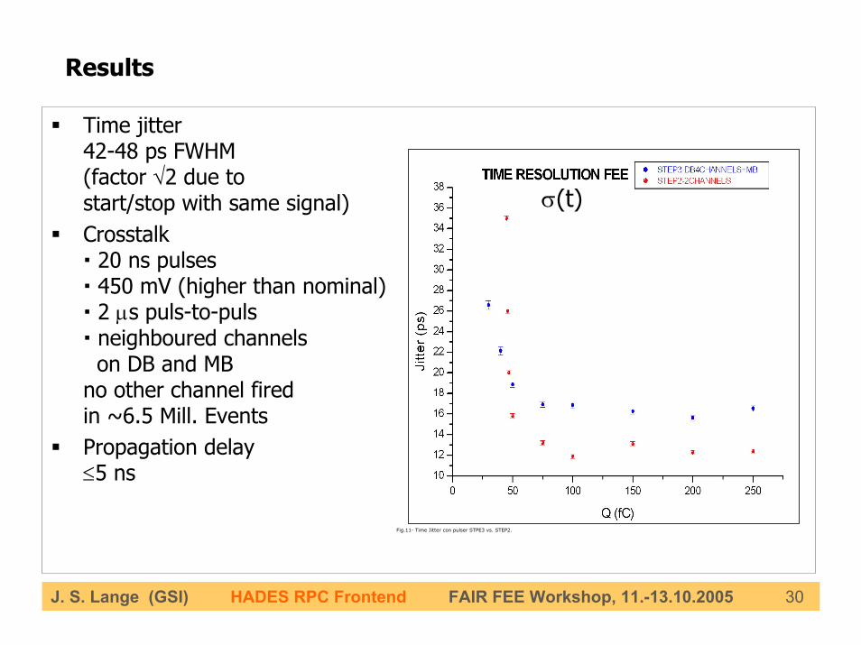
Results
Time jitter42-48 ps FWHM(factor √2 due tostart/stop with same signal)Crosstalk
20 ns pulses 450 mV (higher than nominal)2 µs puls-to-pulsneighboured channelson DB and MB
no other channel firedin ~6.5 Mill. EventsPropagation delay≤5 ns
Fig.11- Time Jitter con pulser STPE3 vs. STEP2.
σ(t)
J. S. Lange (GSI) HADES RPC Frontend FAIR FEE Workshop, 11.-13.10.2005 31
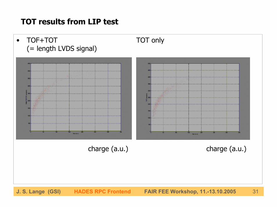
TOT results from LIP test
• TOF+TOT TOT only(= length LVDS signal)
charge (a.u.) charge (a.u.)
J. S. Lange (GSI) HADES RPC Frontend FAIR FEE Workshop, 11.-13.10.2005 32
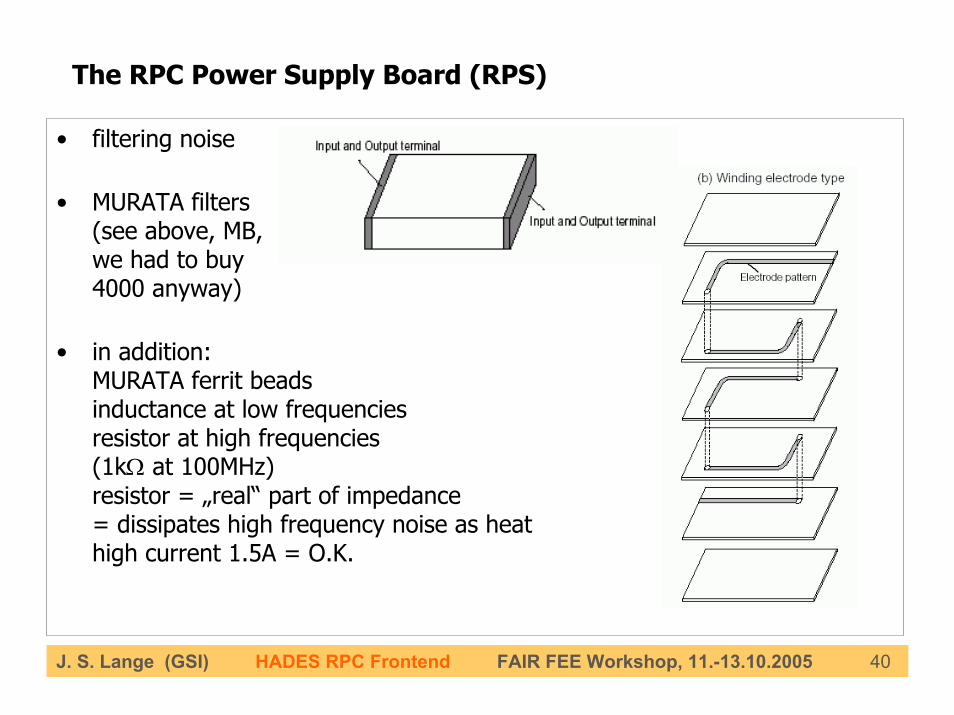
The RPC Power Supply Board (RPS)
• former concept (e.g. HADES drift chambers)LV (e.g. +5V) from power supply over long cable (10 m) to LDOs at the detectorcommon ground
• new concept:point-of-loadsupply +48 V with low current over 10 m cablethen use DC-DC converters with wide input voltage range (35-70 V)(and get high current)
• LDOs ?recent DC-DC converters have comparable ripple and stability~20-50 mV
• ground loops ? No. Use galvanic separation.
• Use MURATA filters• Use MURATA ferrit beads
J. S. Lange (GSI) HADES RPC Frontend FAIR FEE Workshop, 11.-13.10.2005 33
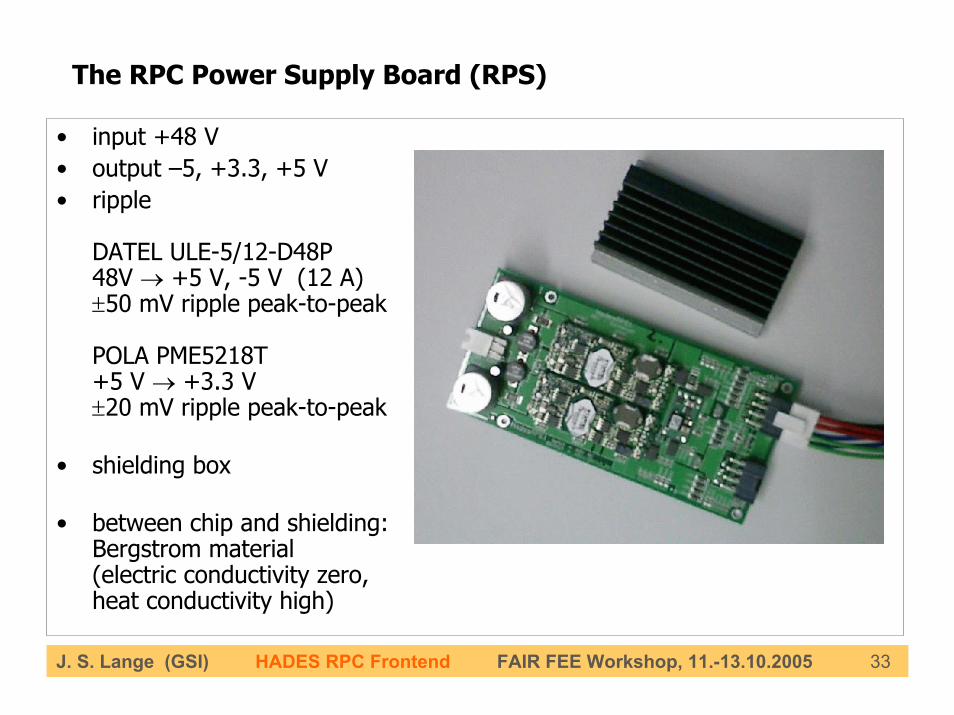
The RPC Power Supply Board (RPS)
• input +48 V• output –5, +3.3, +5 V• ripple
DATEL ULE-5/12-D48P48V → +5 V, -5 V (12 A)±50 mV ripple peak-to-peak
POLA PME5218T+5 V → +3.3 V±20 mV ripple peak-to-peak
• shielding box
• between chip and shielding:Bergstrom material(electric conductivity zero,heat conductivity high)
J. S. Lange (GSI) HADES RPC Frontend FAIR FEE Workshop, 11.-13.10.2005 34
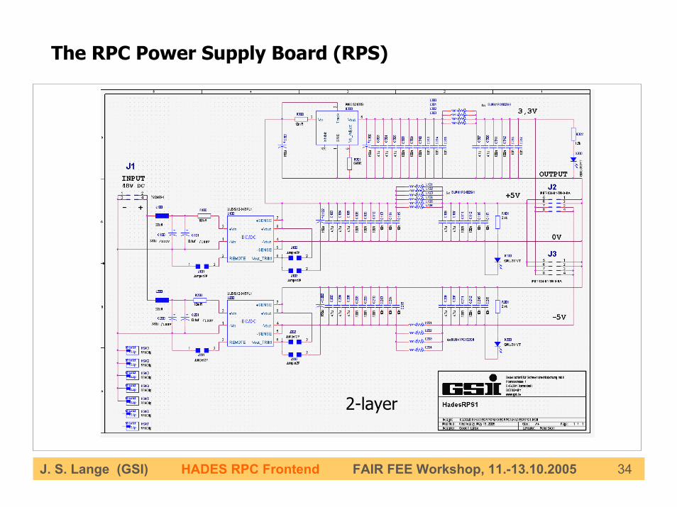
The RPC Power Supply Board (RPS)
2-layer
J. S. Lange (GSI) HADES RPC Frontend FAIR FEE Workshop, 11.-13.10.2005 35
Outlook
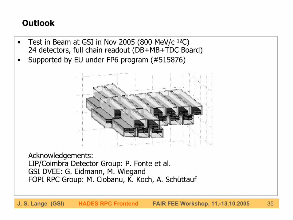
• Test in Beam at GSI in Nov 2005 (800 MeV/c 12C)24 detectors, full chain readout (DB+MB+TDC Board)
• Supported by EU under FP6 program (#515876)
Acknowledgements:LIP/Coimbra Detector Group: P. Fonte et al.GSI DVEE: G. Eidmann, M. WiegandFOPI RPC Group: M. Ciobanu, K. Koch, A. Schüttauf
J. S. Lange (GSI) HADES RPC Frontend FAIR FEE Workshop, 11.-13.10.2005 36
Additional Slides
J. S. Lange (GSI) HADES RPC Frontend FAIR FEE Workshop, 11.-13.10.2005 37
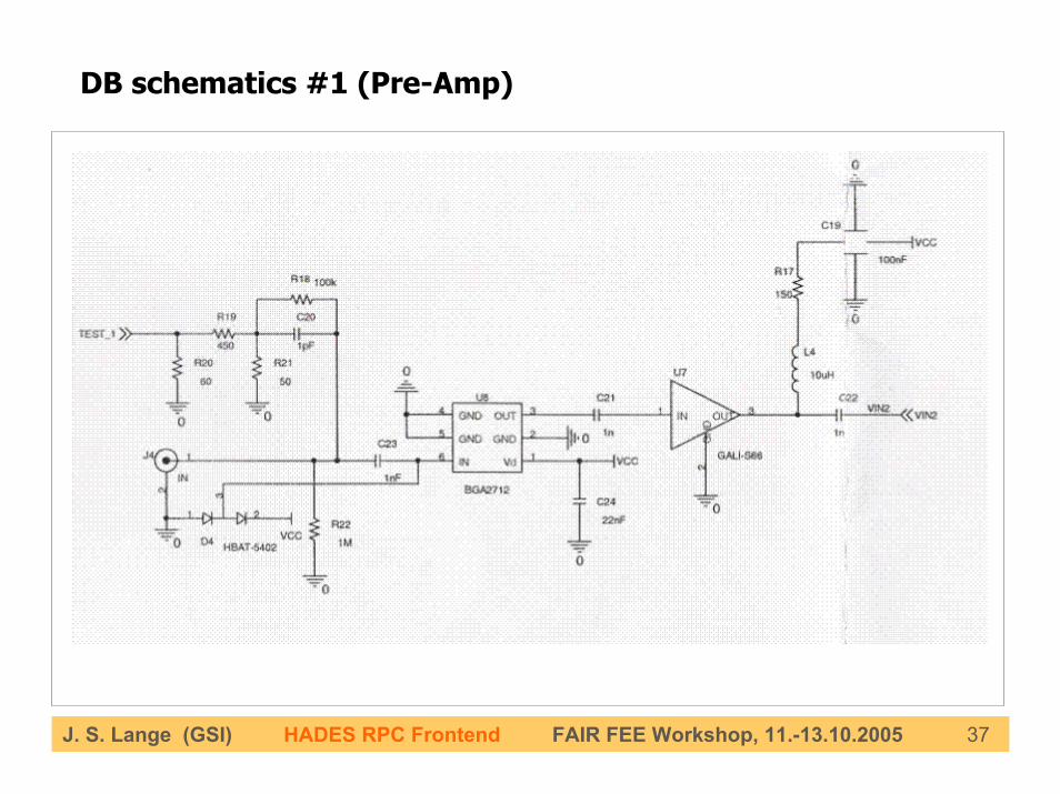
DB schematics #1 (Pre-Amp)
J. S. Lange (GSI) HADES RPC Frontend FAIR FEE Workshop, 11.-13.10.2005 38
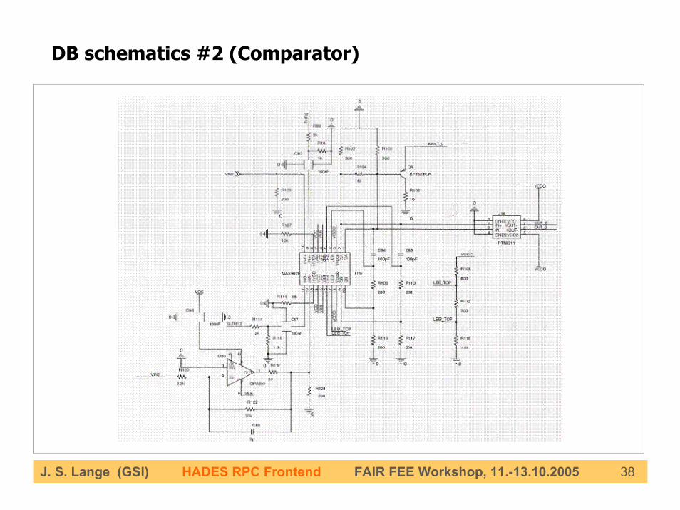
DB schematics #2 (Comparator)
J. S. Lange (GSI) HADES RPC Frontend FAIR FEE Workshop, 11.-13.10.2005 39
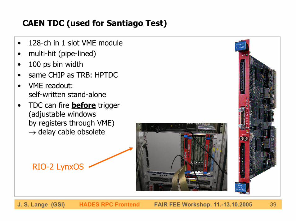
CAEN TDC (used for Santiago Test)
• 128-ch in 1 slot VME module• multi-hit (pipe-lined)• 100 ps bin width• same CHIP as TRB: HPTDC• VME readout:
self-written stand-alone• TDC can fire before trigger
(adjustable windowsby registers through VME)→ delay cable obsolete
RIO-2 LynxOS
J. S. Lange (GSI) HADES RPC Frontend FAIR FEE Workshop, 11.-13.10.2005 40
The RPC Power Supply Board (RPS)
• filtering noise
• MURATA filters (see above, MB,we had to buy 4000 anyway)
• in addition: MURATA ferrit beadsinductance at low frequenciesresistor at high frequencies(1kΩ at 100MHz)resistor = „real“ part of impedance= dissipates high frequency noise as heat high current 1.5A = O.K.
J. S. Lange (GSI) HADES RPC Frontend FAIR FEE Workshop, 11.-13.10.2005 41
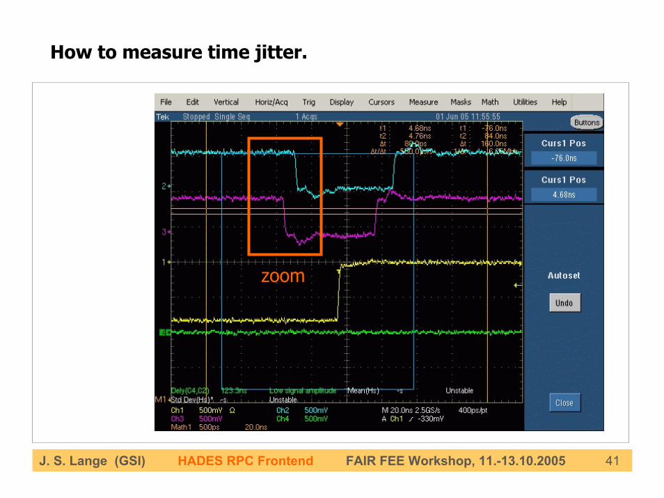
How to measure time jitter.
zoom
J. S. Lange (GSI) HADES RPC Frontend FAIR FEE Workshop, 11.-13.10.2005 42
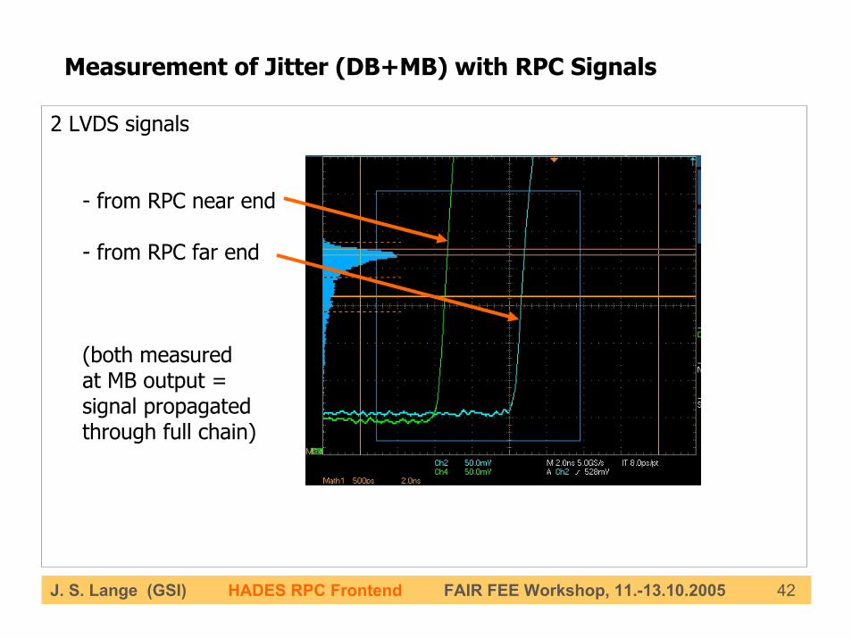
Measurement of Jitter (DB+MB) with RPC Signals
2 LVDS signals
- from RPC near end
- from RPC far end
(both measuredat MB output = signal propagatedthrough full chain)
J. S. Lange (GSI) HADES RPC Frontend FAIR FEE Workshop, 11.-13.10.2005 43
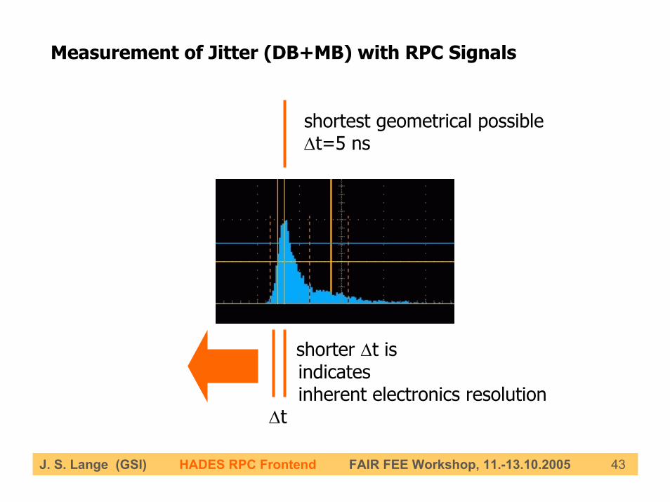
Measurement of Jitter (DB+MB) with RPC Signals
shortest geometrical possible∆t=5 ns
shorter ∆t is indicates inherent electronics resolution
∆t
J. S. Lange (GSI) HADES RPC Frontend FAIR FEE Workshop, 11.-13.10.2005 44
Trigger on MB
• RPC multiplicity signal• inverting op-amp‘s for summing• design:
- use the fact that high level of last pnp stage on DB (+3.2 V)- and also close to +3.3V supply on DB
• 3 stages:
low high(zero fired) (all fired)
stage #1 4-ch +2.4 V +3.2 V on DBstage #2 16-ch +3.2 V +4.0 V= pECL on MBstage #3 31-ch 0 V -3.2 V = nTTL on MB
• LEMO out• op-amp‘s on stage #2 are on GND, but on stage #3 on –5 V
J. S. Lange (GSI) HADES RPC Frontend FAIR FEE Workshop, 11.-13.10.2005 45
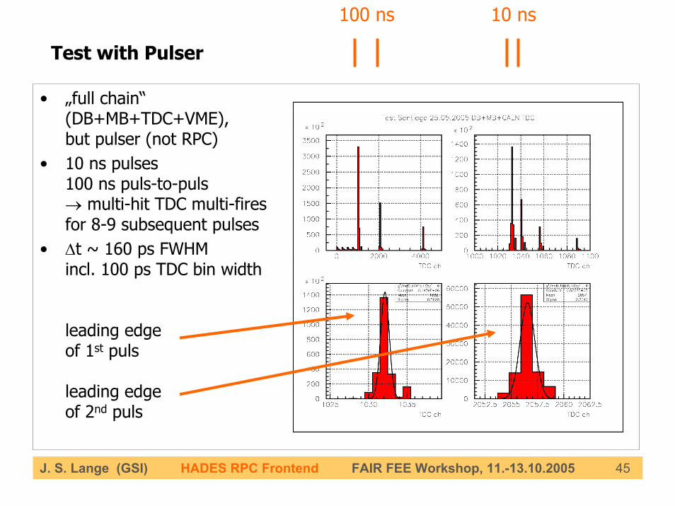
100 ns 10 ns
Test with Pulser
• „full chain“(DB+MB+TDC+VME),but pulser (not RPC)
• 10 ns pulses100 ns puls-to-puls→ multi-hit TDC multi-fires for 8-9 subsequent pulses
• ∆t ~ 160 ps FWHMincl. 100 ps TDC bin width
leading edgeof 1st puls
leading edgeof 2nd puls
J. S. Lange (GSI) HADES RPC Frontend FAIR FEE Workshop, 11.-13.10.2005 46
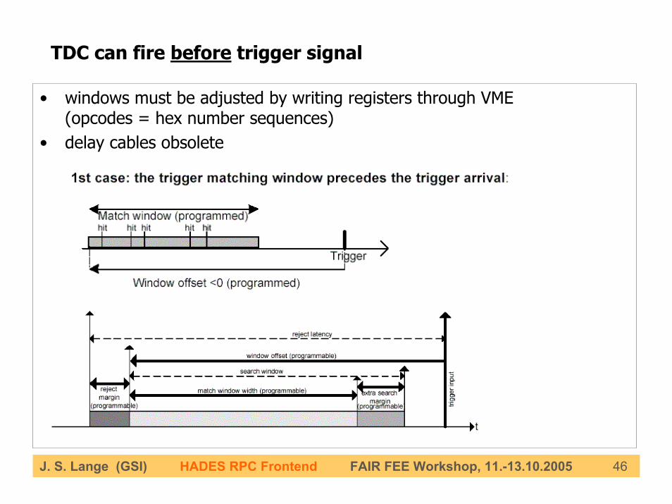
TDC can fire before trigger signal
• windows must be adjusted by writing registers through VME(opcodes = hex number sequences)
• delay cables obsolete