Embed Size (px)
Citation preview
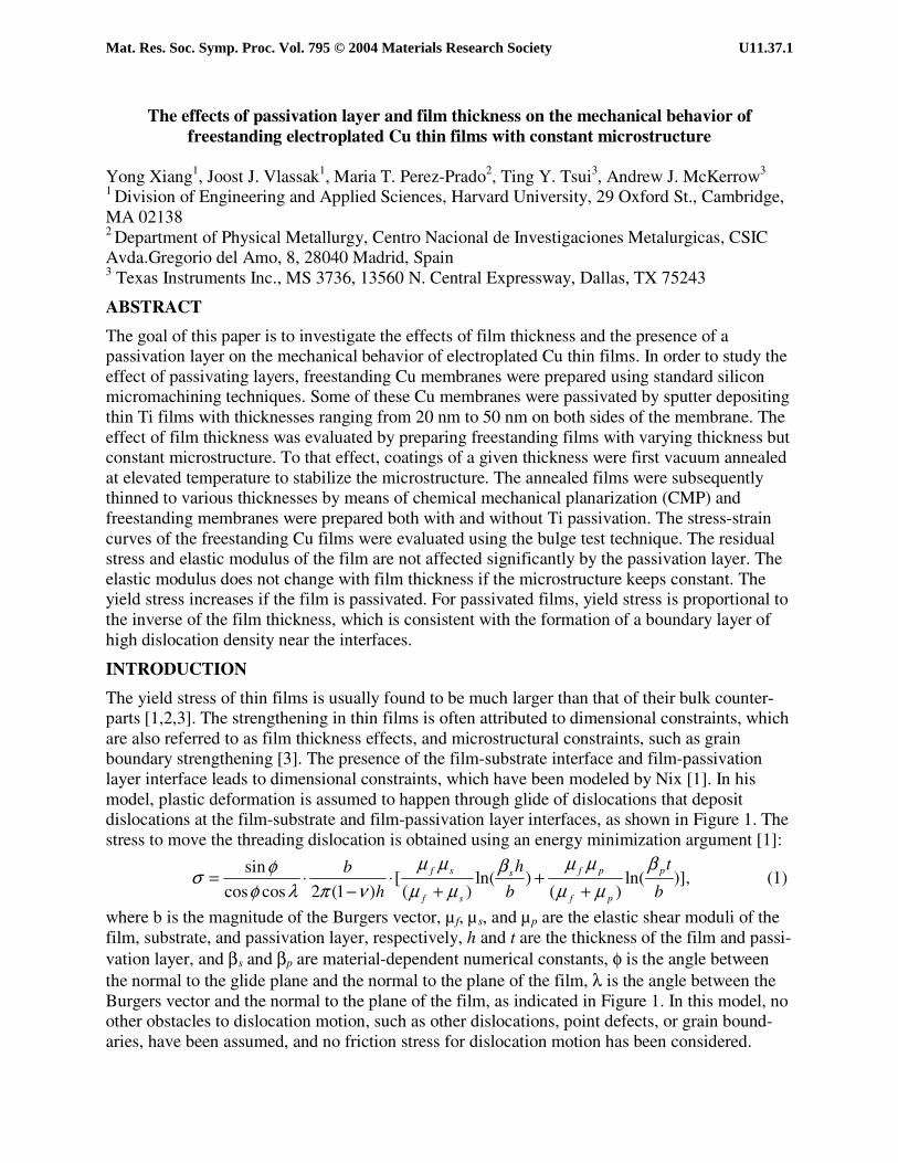
The effects of passivation layer and film thickness on the mechanical behavior of freestanding electroplated Cu thin films with constant microstructure
Yong Xiang1, Joost J. Vlassak1, Maria T. Perez-Prado2, Ting Y. Tsui3, Andrew J. McKerrow3 1 Division of Engineering and Applied Sciences, Harvard University, 29 Oxford St., Cambridge, MA 02138 2 Department of Physical Metallurgy, Centro Nacional de Investigaciones Metalurgicas, CSIC Avda.Gregorio del Amo, 8, 28040 Madrid, Spain 3 Texas Instruments Inc., MS 3736, 13560 N. Central Expressway, Dallas, TX 75243
ABSTRACT
The goal of this paper is to investigate the effects of film thickness and the presence of a passivation layer on the mechanical behavior of electroplated Cu thin films. In order to study the effect of passivating layers, freestanding Cu membranes were prepared using standard silicon micromachining techniques. Some of these Cu membranes were passivated by sputter depositing thin Ti films with thicknesses ranging from 20 nm to 50 nm on both sides of the membrane. The effect of film thickness was evaluated by preparing freestanding films with varying thickness but constant microstructure. To that effect, coatings of a given thickness were first vacuum annealed at elevated temperature to stabilize the microstructure. The annealed films were subsequently thinned to various thicknesses by means of chemical mechanical planarization (CMP) and freestanding membranes were prepared both with and without Ti passivation. The stress-strain curves of the freestanding Cu films were evaluated using the bulge test technique. The residual stress and elastic modulus of the film are not affected significantly by the passivation layer. The elastic modulus does not change with film thickness if the microstructure keeps constant. The yield stress increases if the film is passivated. For passivated films, yield stress is proportional to the inverse of the film thickness, which is consistent with the formation of a boundary layer of high dislocation density near the interfaces.
INTRODUCTION
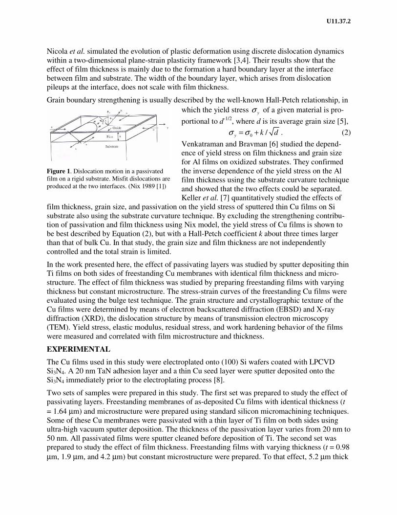
The yield stress of thin films is usually found to be much larger than that of their bulk counter-parts [1,2,3]. The strengthening in thin films is often attributed to dimensional constraints, which are also referred to as film thickness effects, and microstructural constraints, such as grain boundary strengthening [3]. The presence of the film-substrate interface and film-passivation layer interface leads to dimensional constraints, which have been modeled by Nix [1]. In his model, plastic deformation is assumed to happen through glide of dislocations that deposit dislocations at the film-substrate and film-passivation layer interfaces, as shown in Figure 1. The stress to move the threading dislocation is obtained using an energy minimization argument [1]:
)],ln()(
)ln()(
[)1(2coscos
sin
b
t
b
h
h
b p
pf
pfs
sf
sf βµµ
µµβµµ
µµνπλφ
φσ+
++
⋅−
⋅= (1)
where b is the magnitude of the Burgers vector, µ f, µ s, and µp are the elastic shear moduli of the film, substrate, and passivation layer, respectively, h and t are the thickness of the film and passi-vation layer, and βs and βp are material-dependent numerical constants, φ is the angle between the normal to the glide plane and the normal to the plane of the film, λ is the angle between the Burgers vector and the normal to the plane of the film, as indicated in Figure 1. In this model, no other obstacles to dislocation motion, such as other dislocations, point defects, or grain bound-aries, have been assumed, and no friction stress for dislocation motion has been considered.
Mat. Res. Soc. Symp. Proc. Vol. 795 © 2004 Materials Research Society U11.37.1
Nicola et al. simulated the evolution of plastic deformation using discrete dislocation dynamics within a two-dimensional plane-strain plasticity framework [3,4]. Their results show that the effect of film thickness is mainly due to the formation a hard boundary layer at the interface between film and substrate. The width of the boundary layer, which arises from dislocation pileups at the interface, does not scale with film thickness.
Grain boundary strengthening is usually described by the well-known Hall-Petch relationship, in which the yield stress yσ of a given material is pro-
portional to d-1/2, where d is its average grain size [5],
0 /y k dσ σ= + . (2)
Venkatraman and Bravman [6] studied the depend-ence of yield stress on film thickness and grain size for Al films on oxidized substrates. They confirmed the inverse dependence of the yield stress on the Al film thickness using the substrate curvature technique and showed that the two effects could be separated. Keller et al. [7] quantitatively studied the effects of
film thickness, grain size, and passivation on the yield stress of sputtered thin Cu films on Si substrate also using the substrate curvature technique. By excluding the strengthening contribu-tion of passivation and film thickness using Nix model, the yield stress of Cu films is shown to be best described by Equation (2), but with a Hall-Petch coefficient k about three times larger than that of bulk Cu. In that study, the grain size and film thickness are not independently controlled and the total strain is limited.
In the work presented here, the effect of passivating layers was studied by sputter depositing thin Ti films on both sides of freestanding Cu membranes with identical film thickness and micro-structure. The effect of film thickness was studied by preparing freestanding films with varying thickness but constant microstructure. The stress-strain curves of the freestanding Cu films were evaluated using the bulge test technique. The grain structure and crystallographic texture of the Cu films were determined by means of electron backscattered diffraction (EBSD) and X-ray diffraction (XRD), the dislocation structure by means of transmission electron microscopy (TEM). Yield stress, elastic modulus, residual stress, and work hardening behavior of the films were measured and correlated with film microstructure and thickness.
EXPERIMENTAL
The Cu films used in this study were electroplated onto (100) Si wafers coated with LPCVD Si3N4. A 20 nm TaN adhesion layer and a thin Cu seed layer were sputter deposited onto the Si3N4 immediately prior to the electroplating process [8].
Two sets of samples were prepared in this study. The first set was prepared to study the effect of passivating layers. Freestanding membranes of as-deposited Cu films with identical thickness (t = 1.64 µm) and microstructure were prepared using standard silicon micromachining techniques. Some of these Cu membranes were passivated with a thin layer of Ti film on both sides using ultra-high vacuum sputter deposition. The thickness of the passivation layer varies from 20 nm to 50 nm. All passivated films were sputter cleaned before deposition of Ti. The second set was prepared to study the effect of film thickness. Freestanding films with varying thickness (t = 0.98 µm, 1.9 µm, and 4.2 µm) but constant microstructure were prepared. To that effect, 5.2 µm thick
Figure 1. Dislocation motion in a passivated film on a rigid substrate. Misfit dislocations are produced at the two interfaces. (Nix 1989 [1])
U11.37.2
coatings were first vacuum annealed at 400 °C for 15 min to stabilize the microstructure. The annealed films were subsequently thinned by means of chemical mechanical planarization. For each thickness, freestanding membranes were prepared with three passivation conditions: no passivation, one surface passivated by a 20 nm Ti layer, and both surfaces passivated.
The stress-strain curves of the freestanding Cu films were evaluated using a bulge test apparatus [9]. The grain structure and crystallographic texture of the Cu films were determined by means of electron backscattered diffraction (EBSD) and X-ray diffraction (XRD). Cross-sectional TEM samples were prepared for the passivated films both before and after deformation and the dislocation structure was investigated using a Philips TEM Model 420T.
RESULTS AND DISCUSSION
A. Microstructure characterization
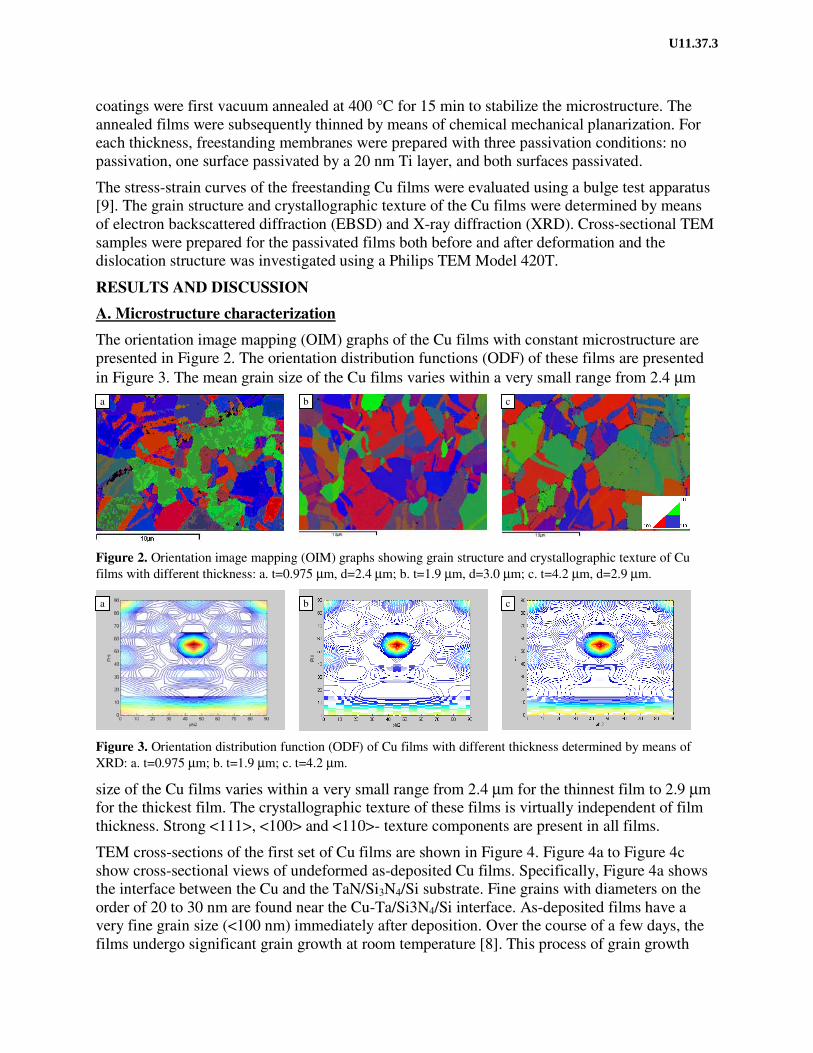
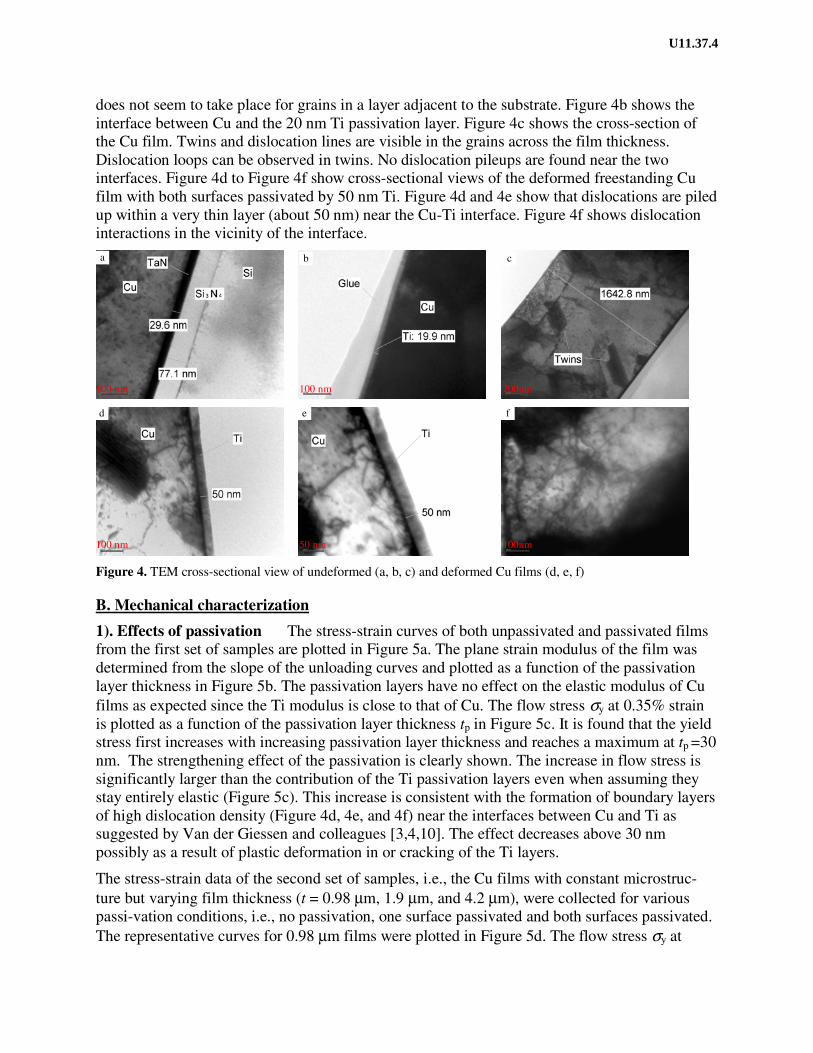
The orientation image mapping (OIM) graphs of the Cu films with constant microstructure are presented in Figure 2. The orientation distribution functions (ODF) of these films are presented in Figure 3. The mean grain size of the Cu films varies within a very small range from 2.4 µm
Figure 2. Orientation image mapping (OIM) graphs showing grain structure and crystallographic texture of Cu films with different thickness: a. t=0.975 µm, d=2.4 µm; b. t=1.9 µm, d=3.0 µm; c. t=4.2 µm, d=2.9 µm.
Figure 3. Orientation distribution function (ODF) of Cu films with different thickness determined by means of XRD: a. t=0.975 µm; b. t=1.9 µm; c. t=4.2 µm.
size of the Cu films varies within a very small range from 2.4 µm for the thinnest film to 2.9 µm for the thickest film. The crystallographic texture of these films is virtually independent of film thickness. Strong <111>, <100> and <110>- texture components are present in all films.
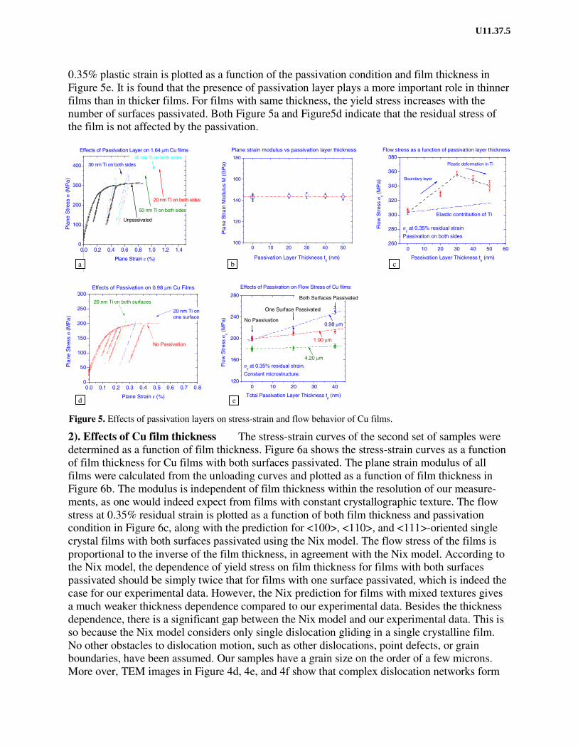
TEM cross-sections of the first set of Cu films are shown in Figure 4. Figure 4a to Figure 4c show cross-sectional views of undeformed as-deposited Cu films. Specifically, Figure 4a shows the interface between the Cu and the TaN/Si3N4/Si substrate. Fine grains with diameters on the order of 20 to 30 nm are found near the Cu-Ta/Si3N4/Si interface. As-deposited films have a very fine grain size (<100 nm) immediately after deposition. Over the course of a few days, the films undergo significant grain growth at room temperature [8]. This process of grain growth
c a b
c a b
U11.37.3
does not seem to take place for grains in a layer adjacent to the substrate. Figure 4b shows the interface between Cu and the 20 nm Ti passivation layer. Figure 4c shows the cross-section of the Cu film. Twins and dislocation lines are visible in the grains across the film thickness. Dislocation loops can be observed in twins. No dislocation pileups are found near the two interfaces. Figure 4d to Figure 4f show cross-sectional views of the deformed freestanding Cu film with both surfaces passivated by 50 nm Ti. Figure 4d and 4e show that dislocations are piled up within a very thin layer (about 50 nm) near the Cu-Ti interface. Figure 4f shows dislocation interactions in the vicinity of the interface.
Figure 4. TEM cross-sectional view of undeformed (a, b, c) and deformed Cu films (d, e, f)
B. Mechanical characterization
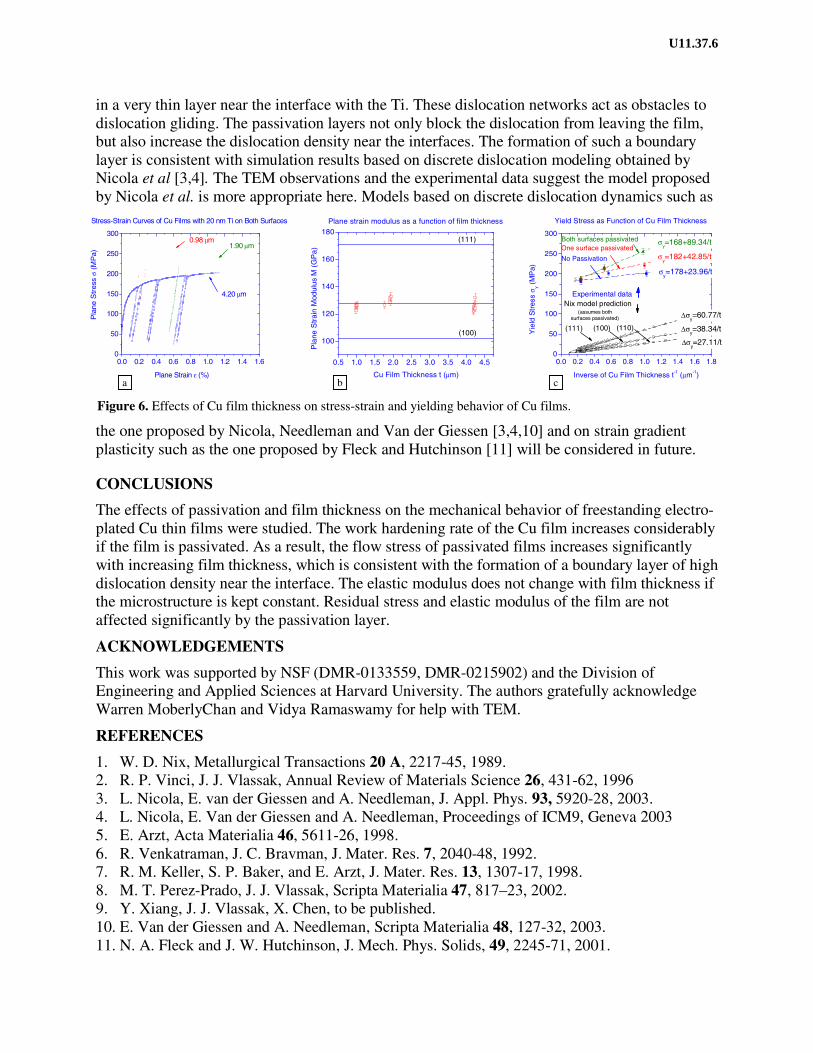
1). Effects of passivation The stress-strain curves of both unpassivated and passivated films from the first set of samples are plotted in Figure 5a. The plane strain modulus of the film was determined from the slope of the unloading curves and plotted as a function of the passivation layer thickness in Figure 5b. The passivation layers have no effect on the elastic modulus of Cu films as expected since the Ti modulus is close to that of Cu. The flow stress σy at 0.35% strain is plotted as a function of the passivation layer thickness tp in Figure 5c. It is found that the yield stress first increases with increasing passivation layer thickness and reaches a maximum at tp =30 nm. The strengthening effect of the passivation is clearly shown. The increase in flow stress is significantly larger than the contribution of the Ti passivation layers even when assuming they stay entirely elastic (Figure 5c). This increase is consistent with the formation of boundary layers of high dislocation density (Figure 4d, 4e, and 4f) near the interfaces between Cu and Ti as suggested by Van der Giessen and colleagues [3,4,10]. The effect decreases above 30 nm possibly as a result of plastic deformation in or cracking of the Ti layers.
The stress-strain data of the second set of samples, i.e., the Cu films with constant microstruc-ture but varying film thickness (t = 0.98 µm, 1.9 µm, and 4.2 µm), were collected for various passi-vation conditions, i.e., no passivation, one surface passivated and both surfaces passivated. The representative curves for 0.98 µm films were plotted in Figure 5d. The flow stress σy at
b c a
d e f
100 nm
100 nm 100 nm
50 nm
200nm
100nm
U11.37.4
0.35% plastic strain is plotted as a function of the passivation condition and film thickness in Figure 5e. It is found that the presence of passivation layer plays a more important role in thinner films than in thicker films. For films with same thickness, the yield stress increases with the number of surfaces passivated. Both Figure 5a and Figure5d indicate that the residual stress of the film is not affected by the passivation.
0.0 0.2 0.4 0.6 0.8 1.0 1.2 1.40
100
200
300
400
40 nm Ti on both sides
20 nm Ti on both sides
Unpassivated
Effects of Passivation Layer on 1.64 µm Cu films
Pla
ne S
tres
s σ
(MP
a)
Plane Strain ε (%)
50 nm Ti on both sides
30 nm Ti on both sides
0 10 20 30 40 50100
120
140
160
180
Plane strain modulus vs passivation layer thickness
Pla
ne S
trai
n M
odul
us M
(G
Pa)
Passivation Layer Thickness tp (nm)
0 10 20 30 40 50 60260
280
300
320
340
360
380Flow stress as a function of passivation layer thickness
Flo
w S
tres
s σ y
(MP
a)
Passivation Layer Thickness tp (nm)
σy at 0.35% residual strain
Passivation on both sides
Elastic contribution of Ti
Boundary layer
Plastic deformation in Ti
0.0 0.1 0.2 0.3 0.4 0.5 0.6 0.7 0.80
50
100
150
200
250
300
20 nm Ti on both surfaces
20 nm Ti on one surface
No Passivation
Effects of Passivation on 0.98 µm Cu Films
Pla
ne S
tres
s σ
(MP
a)
Plane Strain ε (%)
0 10 20 30 40120
160
200
240
280
4.20 µm
1.90 µm
0.98 µm
Effects of Passivation on Flow Stress of Cu films
σy at 0.35% residual strain.
Constant microstructure.
Both Surfaces Passivated
One Surface Passivated
No Passivation
Flo
w S
tres
s σ y (
MP
a)
Total Passivation Layer Thickness tp (nm)
Figure 5. Effects of passivation layers on stress-strain and flow behavior of Cu films.
2). Effects of Cu film thickness The stress-strain curves of the second set of samples were determined as a function of film thickness. Figure 6a shows the stress-strain curves as a function of film thickness for Cu films with both surfaces passivated. The plane strain modulus of all films were calculated from the unloading curves and plotted as a function of film thickness in Figure 6b. The modulus is independent of film thickness within the resolution of our measure-ments, as one would indeed expect from films with constant crystallographic texture. The flow stress at 0.35% residual strain is plotted as a function of both film thickness and passivation condition in Figure 6c, along with the prediction for <100>, <110>, and <111>-oriented single crystal films with both surfaces passivated using the Nix model. The flow stress of the films is proportional to the inverse of the film thickness, in agreement with the Nix model. According to the Nix model, the dependence of yield stress on film thickness for films with both surfaces passivated should be simply twice that for films with one surface passivated, which is indeed the case for our experimental data. However, the Nix prediction for films with mixed textures gives a much weaker thickness dependence compared to our experimental data. Besides the thickness dependence, there is a significant gap between the Nix model and our experimental data. This is so because the Nix model considers only single dislocation gliding in a single crystalline film. No other obstacles to dislocation motion, such as other dislocations, point defects, or grain boundaries, have been assumed. Our samples have a grain size on the order of a few microns. More over, TEM images in Figure 4d, 4e, and 4f show that complex dislocation networks form
a b c
d e
U11.37.5
in a very thin layer near the interface with the Ti. These dislocation networks act as obstacles to dislocation gliding. The passivation layers not only block the dislocation from leaving the film, but also increase the dislocation density near the interfaces. The formation of such a boundary layer is consistent with simulation results based on discrete dislocation modeling obtained by Nicola et al [3,4]. The TEM observations and the experimental data suggest the model proposed by Nicola et al. is more appropriate here. Models based on discrete dislocation dynamics such as
0.0 0.2 0.4 0.6 0.8 1.0 1.2 1.4 1.60
50
100
150
200
250
3000.98 µm
1.90 µm
4.20 µm
Plane Strain ε (%)
Pla
ne S
tres
s σ
(MP
a)
Stress-Strain Curves of Cu Films with 20 nm Ti on Both Surfaces
0.5 1.0 1.5 2.0 2.5 3.0 3.5 4.0 4.5
100
120
140
160
180
Pla
ne S
trai
n M
odul
us M
(G
Pa)
Cu Film Thickness t (µm)
(100)
(111)
Plane strain modulus as a function of film thickness
0.0 0.2 0.4 0.6 0.8 1.0 1.2 1.4 1.6 1.80
50
100
150
200
250
300
(110)(100)
Nix model prediction (assumes both surfaces passivated)
Yield Stress as Function of Cu Film Thickness
σy=178+23.96/t
σy=182+42.85/t
σy=168+89.34/t
∆σy=27.11/t
∆σy=38.34/t
∆σy=60.77/t
Yie
ld S
tres
s σ y (
MP
a)
Inverse of Cu Film Thickness t-1 (µm-1)
Experimental data
(111)
No Passivation
One surface passivatedBoth surfaces passivated
Figure 6. Effects of Cu film thickness on stress-strain and yielding behavior of Cu films.
the one proposed by Nicola, Needleman and Van der Giessen [3,4,10] and on strain gradient plasticity such as the one proposed by Fleck and Hutchinson [11] will be considered in future.
CONCLUSIONS
The effects of passivation and film thickness on the mechanical behavior of freestanding electro-plated Cu thin films were studied. The work hardening rate of the Cu film increases considerably if the film is passivated. As a result, the flow stress of passivated films increases significantly with increasing film thickness, which is consistent with the formation of a boundary layer of high dislocation density near the interface. The elastic modulus does not change with film thickness if the microstructure is kept constant. Residual stress and elastic modulus of the film are not affected significantly by the passivation layer.
ACKNOWLEDGEMENTS
This work was supported by NSF (DMR-0133559, DMR-0215902) and the Division of Engineering and Applied Sciences at Harvard University. The authors gratefully acknowledge Warren MoberlyChan and Vidya Ramaswamy for help with TEM.
REFERENCES
1. W. D. Nix, Metallurgical Transactions 20 A, 2217-45, 1989. 2. R. P. Vinci, J. J. Vlassak, Annual Review of Materials Science 26, 431-62, 1996 3. L. Nicola, E. van der Giessen and A. Needleman, J. Appl. Phys. 93, 5920-28, 2003. 4. L. Nicola, E. Van der Giessen and A. Needleman, Proceedings of ICM9, Geneva 2003 5. E. Arzt, Acta Materialia 46, 5611-26, 1998. 6. R. Venkatraman, J. C. Bravman, J. Mater. Res. 7, 2040-48, 1992. 7. R. M. Keller, S. P. Baker, and E. Arzt, J. Mater. Res. 13, 1307-17, 1998. 8. M. T. Perez-Prado, J. J. Vlassak, Scripta Materialia 47, 817–23, 2002. 9. Y. Xiang, J. J. Vlassak, X. Chen, to be published. 10. E. Van der Giessen and A. Needleman, Scripta Materialia 48, 127-32, 2003. 11. N. A. Fleck and J. W. Hutchinson, J. Mech. Phys. Solids, 49, 2245-71, 2001.
b c a
U11.37.6