Embed Size (px)
Citation preview
Journal of Crystal Growth 198/199 (1999) 1032—1038
The effect of mismatch strain on Stranski—Krastanow transitionin epitaxial Ge
xSi
1~x/Si(0 0 1) gas-source growth
I. Goldfarb*, G.A.D. BriggsDepartment of Materials, University of Oxford, Parks Road, Oxford OX1 3PH, UK
Abstract
Mechanisms of strain-relief during epitaxial growth of Ge0.6
Si0.4
/Si(0 0 1) alloy at 500°C have been investigated usingin situ scanning tunneling microscopy. The reduction of mismatch strain due to reduced Ge content of the epilayer (2.6%relative to 4.2% in Ge/Si(0 0 1)) has a profound effect not only on the final film morphology, but seem to alter the entiresequence of intermediate surface morphologies which, under these conditions, is dominated by layer-mounding ratherthan by faceting. Low-angle facets (+6°), different from the 11°-M5 0 1N facets in the case of pure Ge/Si(0 0 1), appear onlyat the final stages of growth. Understanding of roughening transitions in strained-layer growth is essential for controllingthe cluster size and geometry for applications in quantum dot devices. ( 1999 Elsevier Science B.V. All rights reserved.
PACS: 81.15.Kk; 61.16.Ch; 68.35.Bs; 68.65.#g
Keywords: Heteroepitaxy; Strain relaxation; Three-dimensional islands; Silicon; Germanium
1. Introduction
It has been recognised in the past decade thatstrained epilayers, e.g. Ge
xSi
1~x/Si(0 0 1), where
0(x(1, are metastable against surface roughen-ing via three-dimensional (3D) faceted islandsand ripples [1—8]. Since Ge
xSi
1~x/Si is a
Stranski—Krastanow (SK) growth system, the firstfew monolayers (ML) form pseudomorphic two-
*Corresponding author. Fax: #44 1865 273 783; e-mail:[email protected].
dimensional (2D) wetting layer, prior to 3Droughening [9]. The kinetic route for strain relax-ation exhibits a series of fascinating phenomenabefore reaching the final state of large 3D islandsrelaxed by dislocations: formation of two types ofperiodic vacancy lines [9—12] and the resultantreversal of the both surface stress anisotropy andstep roughness [13,14], roughness dependence onthe sign of the strain and triangular step insta-bilities [15—17], formation of various pyramidalmicro- and macro-clusters with different facets[2,9,11,12], surface undulations [3,4,6—8] and, aswe have recently demonstrated, the strain can alsobe partially relaxed via formation of pyramidalmicro-pits [11].
0022-0248/99/$ — see front matter ( 1999 Elsevier Science B.V. All rights reserved.PII: S 0 0 2 2 - 0 2 4 8 ( 9 8 ) 0 0 9 7 9 - 8
In this letter we shed some light on this complexissue by real-time elevated-temperature scanningtunneling microscopy (STM) observation ofGe
0.6Si
0.4/Si(0 0 1) growth from GeH
4and Si
2H
6.
In order to increase the energy barrier for facetedislanding (which is extremely sensitive to strain [5])the mismatch strain was reduced by introduction ofSi into the growing film, however the ratio of par-tial GeH
4and Si
2H
6pressures was adjusted to
10 : 1 to ensure sufficient Ge presence (x'0.5) forinitial strain relief by roughening rather than bydislocations [5,6]. Such a reduction of strain inconjunction with relatively high growth temper-ature of 500°C was chosen to reduce the tendencyfor micro-hut formation [2]. As will be shown, suchconditions lead to a sequence of surface structuresdifferent from those observed at lower temper-atures and higher strains [11,12].
2. Experimental procedure
After ex vacuo chemical treatment the Si sampleswere introduced into a UHV JEOL JSTM-4500XTcapable of operation up to 1250°C, degassed forseveral hours and repeatedly flashed at 1200°C(keeping the pressure below 10~7 Pa) before slowcooling to the desired temperature. Such treatmenthas generally proved effective in producing atomi-cally flat good quality Si(0 0 1)-(2]1)&(1]2) surfa-ces free of mounds or pits [11,12,18]. The imageswere taken using electrochemically etched ¼ tipsat 500°C (achieved by direct current resistive heat-ing and measured by optical pyrometer with$30°C accuracy) in the “constant current” mode,with tunneling current of 0.08 nA and sample biasof !2 V while the 10 : 1 GeH
4: Si
2H
6mixture was
fed through a precision-valve onto the samplemounted in the STM stage at a desired constantpressure in the 2]10~5—4]10~5 Pa range. Thecoverage was determined by computerised subtrac-tion of submonolayer images from one another,after fixing the same fiducial points in each success-ive pair of images. The eventual thickness and theGe content of the grown layer were measured usingsecondary ion mass spectroscopy (SIMS) depthprofiling with a 7.5 keV, 5 nA O`
2primary
beam. A reference sample with a 80 nm-thick
Ge0.2
Si0.8
/Si(0 0 1) epilayer was used to calibratethe elemental sensitivity factors and the sputteringrate (which was also confirmed from the depth ofthe sputtered crater).
3. Results and discussion
SIMS depth profile of the grown GexSi
1~xepi-
layer is shown in Fig. 1 and exhibits three distinctregions: close to the surface, after the initial transi-ent the profiles are relatively flat with a constantSi : Ge ratio (“epi”), followed by a region of grad-ually changing (“intermixed”) signals, which we at-tribute to sputter-induced atomic mixing and recoilimplantation (e.g. see Ref. [19]), and, finally, belowabout 10 nm the profiles settle to values character-istic of the substrate, with some residual mixing ofthe Ge. Taking all these effects into account, espe-cially sputtering of the Ge atoms over a depth ofmore than 10 nm, we estimate the Ge concentra-tion of the epilayer to be 62%, which agrees withthe composition to be expected from the 10 : 1GeH
4: Si
2H
6mixture [20,21], and the epilayer
thickness to be 2.5 nm, which agrees with 17 MLestimated from deposition rate (based on subtrac-tion of successive images). Ge segregation tothe surface was not detected in these SIMS pro-files, although it could be masked by the initialtransients.
Fig. 1. SIMS depth profile of the grown GeSi/Si(0 0 1) epilayer,with 7.5 keV, 5 nA O`
2primary beam (0.4 nm/min sputtering
rate).
I. Goldfarb, G.A.D. Briggs / Journal of Crystal Growth 198/199 (1999) 1032–1038 1033
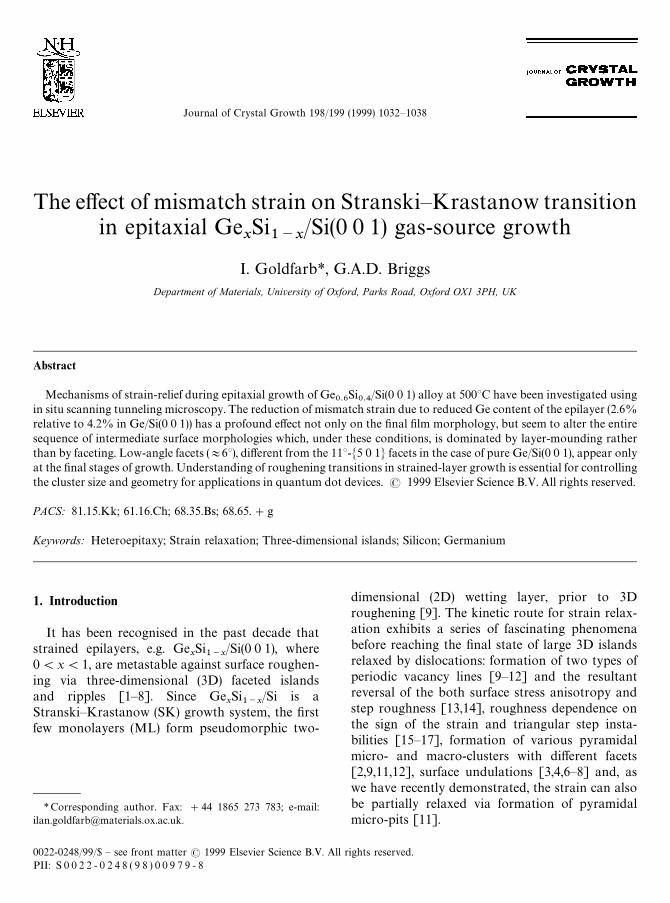
The evolution of surface morphology with cover-age is shown in Fig. 2. The difference between thelow surface coverage and higher coverages is strik-ing: while initially the surface completely resemblesthat of a clean Si (Fig. 2a), with increasing coveragea high density of shallow pits is formed (Fig. 2b),followed by periodic array of dimer-vacancy-lines(DVLs) (Fig. 2c), and finally large faceted clusters(Fig. 2d). While in the case of pure Ge/Si(0 0 1)DVLs and dimer row vacancies (DRVs) were firstto form [12], in the alloy case the pits precededDVLs, and DRVs (forming the (M]N)-recon-structed surface when combined with DVLs [11])did not form at all. Nucleation of the shallow pitsproceeds similarly to that of hut pits observed inour previous work [11]: comparing the pair ofsurface voids in Fig. 2a to the same pair in Fig. 2band Fig. 2c, it can be deduced that the shallow pitsnucleate heterogeneously from the small existingvoids. However these shallow pits (Fig. 3a) differfrom the Ge/Si(0 0 1) hut pits described in our pre-vious work [11] (Fig. 3b): their edges are orientedin the S1 1 0T crystallographic directions, and thewetting layer at the time of their formation is notsufficiently thick to accommodate an inverse pyr-amid, and thus the pits are too shallow to forma facet. Therefore they can mostly expand laterally,without gaining too much depth. Such a growthmode is realised by agglomeration of vacanciesaround the pits (there seems to be an apparentreluctance to fill them), as follows from examina-tion of pit blow-ups in Fig. 3a and in the insets ofFig. 2a, Fig. 2b, and Fig. 2c.
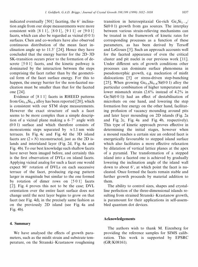
In spite of this initial reluctance, as the growthcontinues the shallow pits are gradually filled andthe strain can no longer be relieved at them, nor itcan be relieved by DVLs since the mutual repulsionprevents them from further multiplication [10].This point occurs at the coverage of 9 ML andindicates the beginning of SK transition. Fig. 4shows an initially 2D island, which with increasingcoverage (Fig. 4a and Fig. 4b) progressivelyevolves into the rather large and faceted 3D is-land (marked “2” in Fig. 2d), as seen in Fig. 4c andFig. 4d. Fig. 5a displays profile plots measuredalong the lines indicated in Fig. 4, and Fig. 5b,demonstrates the island inclination angle depend-ence on coverage. Analysing the changes in cluster
Fig. 2. Progression of Ge0.6
Si0.4
/Si(0 0 1) growth at 500°C:(a) 0.3 ML; (b) 1.8 ML, conversion of voids into shallow pits(c) 3.0 ML: pit growth and formation of (2]N); (d) 12 ML,formation of faceted clusters.
1034 I. Goldfarb, G.A.D. Briggs / Journal of Crystal Growth 198/199 (1999) 1032–1038
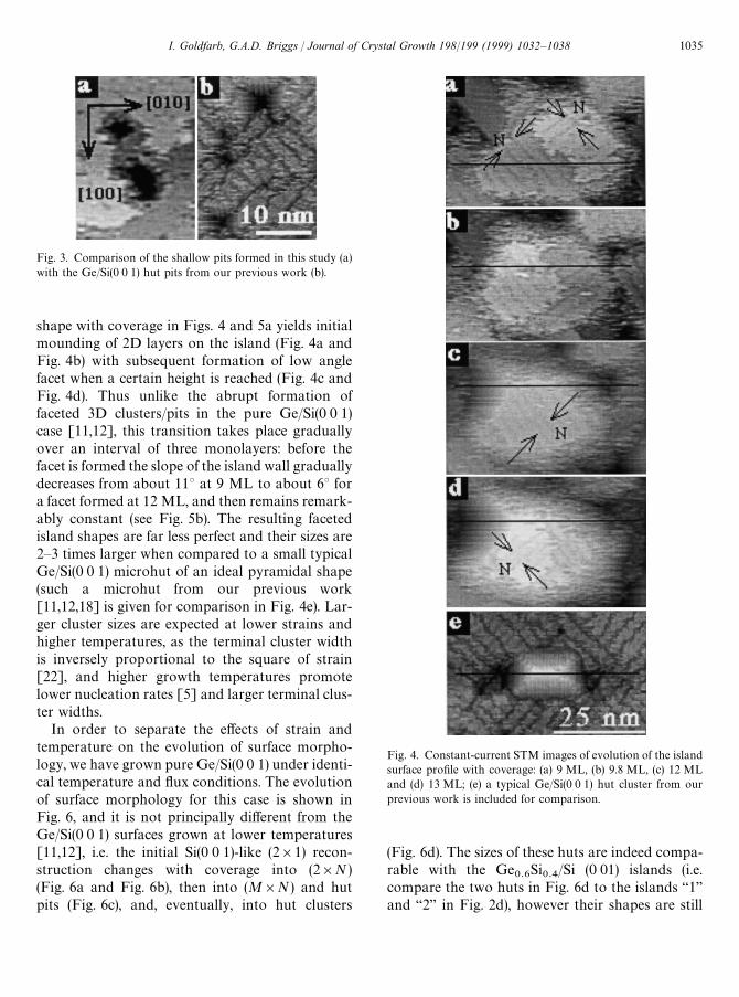
Fig. 3. Comparison of the shallow pits formed in this study (a)with the Ge/Si(0 0 1) hut pits from our previous work (b).
shape with coverage in Figs. 4 and 5a yields initialmounding of 2D layers on the island (Fig. 4a andFig. 4b) with subsequent formation of low anglefacet when a certain height is reached (Fig. 4c andFig. 4d). Thus unlike the abrupt formation offaceted 3D clusters/pits in the pure Ge/Si(0 0 1)case [11,12], this transition takes place graduallyover an interval of three monolayers: before thefacet is formed the slope of the island wall graduallydecreases from about 11° at 9 ML to about 6° fora facet formed at 12 ML, and then remains remark-ably constant (see Fig. 5b). The resulting facetedisland shapes are far less perfect and their sizes are2—3 times larger when compared to a small typicalGe/Si(0 0 1) microhut of an ideal pyramidal shape(such a microhut from our previous work[11,12,18] is given for comparison in Fig. 4e). Lar-ger cluster sizes are expected at lower strains andhigher temperatures, as the terminal cluster widthis inversely proportional to the square of strain[22], and higher growth temperatures promotelower nucleation rates [5] and larger terminal clus-ter widths.
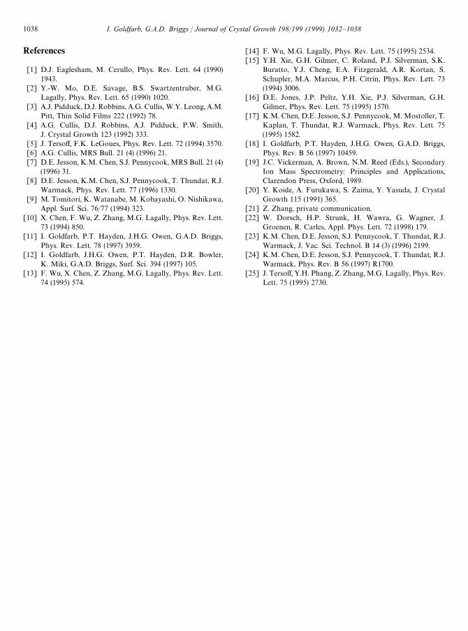
In order to separate the effects of strain andtemperature on the evolution of surface morpho-logy, we have grown pure Ge/Si(0 0 1) under identi-cal temperature and flux conditions. The evolutionof surface morphology for this case is shown inFig. 6, and it is not principally different from theGe/Si(0 0 1) surfaces grown at lower temperatures[11,12], i.e. the initial Si(0 0 1)-like (2]1) recon-struction changes with coverage into (2]N)(Fig. 6a and Fig. 6b), then into (M]N) and hutpits (Fig. 6c), and, eventually, into hut clusters
Fig. 4. Constant-current STM images of evolution of the islandsurface profile with coverage: (a) 9 ML, (b) 9.8 ML, (c) 12 MLand (d) 13 ML; (e) a typical Ge/Si(0 0 1) hut cluster from ourprevious work is included for comparison.
(Fig. 6d). The sizes of these huts are indeed compa-rable with the Ge
0.6Si
0.4/Si (0 01) islands (i.e.
compare the two huts in Fig. 6d to the islands “1”and “2” in Fig. 2d), however their shapes are still
I. Goldfarb, G.A.D. Briggs / Journal of Crystal Growth 198/199 (1999) 1032–1038 1035
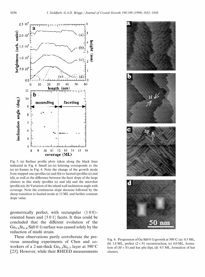
Fig. 5. (a) Surface profile plots taken along the black linesindicated in Fig. 4. Small (a)—(e) lettering corresponds to the(a)—(e) frames in Fig. 4. Note the change of the growth modefrom stepped one (profiles (a) and (b)) to faceted (profiles (c) and(d)), as well as the difference between the facet slope of the largeclusters in this study (profiles (c) and (d)) and the microhut(profile (e)). (b) Variation of the island wall inclination angle withcoverage. Note the continuous slope decrease followed by thesharp transition to faceted mode at 12 ML and further constantslope value.
geometrically perfect, with rectangular S1 0 0T-oriented bases and M5 0 1N facets. It thus could beconcluded that the different evolution of theGe
0.6Si
0.4/Si(0 0 1) surface was caused solely by the
reduction of misfit strain.These observations partly corroborate the pre-
vious annealing experiments of Chen and co-workers of a 2 nm-thick Ge
0.5Si
0.5layer at 590°C
[23]. However, while their RHEED measurements
Fig. 6. Progression of Ge/Si(0 0 1) growth at 500°C: (a) 0.5 ML,(b) 1.8 ML, perfect (2]N) reconstruction, (c) 6.0 ML, forma-tion of (M]N) and hut pits (hp), (d) 9.5 ML, formation of hutclusters.
1036 I. Goldfarb, G.A.D. Briggs / Journal of Crystal Growth 198/199 (1999) 1032–1038
indicated eventually M501N faceting, the 6° inclina-tion angle from our slope measurements were moreconsistent with M8 1 1N, M8 0 1N, M9 1 1N or M9 0 1Nfacets, which can also be regarded as vicinal (0 0 1)surfaces. Chen and co-workers have also observedcontinuous distribution of the mean facet in-clination angle up to 11.3° [24]. Hence they haveconcluded that the energy barrier for the 2D—3DSK-transition occurs prior to the formation of de-screte M5 0 1N facets, and the kinetic pathway isdominated by the interaction between the stepscomprising the facet rather than by the geometri-cal form of the facet surface energy. For this tohappen, the energy barrier for the non-faceted nu-cleation must be smaller than that for the facetedone [24].
Evidence of M8 1 1N facets in RHEED patternsfrom Ge
0.6Si
0.4alloy has been reported [20], which
is consistent with our STM slope measurements.However the exact structure of such a facetseems to be more complex than a simple descrip-tion of a vicinal plane making a 6—7° angle with(0 0 1) surface and which therefore consists ofmonoatomic steps separated by +1.1 nm wideterraces. In Fig. 4c and Fig. 4d the 3D islandfacets are (2]N) reconstructed, just as the 2D is-lands and interisland layer (Fig. 2d, Fig. 4a andFig. 4b). To our best knowledge such shallow facetshave never been imaged before, and certainly thisis the first observation of DVLs on island facets.Applying vicinal analog for such a facet one wouldexpect 90° rotation of DVLs on each successiveterrace of the facet, producing zig-zag patternlarger in magnitude but similar to the one formedby rotation of dimer rows on M5 0 1N facets[2]. Fig. 4 proves this not to be the case; DVLorientation over the entire facet surface does notchange until the next layer begins to grow on thatfacet (see Fig. 4d), in the precisely same fashion ason the previously 2D island (see Fig. 4a andFig. 4b).
4. Summary
We have analysed the effects of growth para-meters, such as the misfit strain and substrate tem-perature, on the Stranski—Krastanow roughening
transition in heteroepitaxial Ge-rich GexSi
1~x/
Si(0 0 1) growth from gas sources. The interplaybetween various strain-relieving mechanisms canbe treated in the framework of kinetic rates forcorresponding processes as a function of theseparameters, as has been derived by Tersoffand LeGoues [5]. Such an approach accounts wellfor the faceted appearance of even the criticalcluster and pit nuclei in our previous work [11].Under different sets of growth conditions otherprocesses can dominate surface phenomena inpseudomorphic growth, e.g. nucleation of misfitdislocations [5] or stress-driven step-bunching[25]. When growing Ge
0.6Si
0.4/Si(0 0 1) alloy the
particular combination of higher temperature andlower mismatch strain (2.6% instead of 4.2% inGe/Si(0 0 1)) had an effect of destabilisation ofmicrohuts on one hand, and lowering the stepformation free energy on the other hand, facilitat-ing profusion of vacancy mounding around pitsand later layer mounding on 2D islands (Fig. 2aand Fig. 2c, Fig. 4a and Fig. 4b, respectively).This type of kinetic approach proves effective indetermining the initial stages, however whena mound reaches a certain size an ordered facet isenergetically favourable to stepped island surfacewhich also facilitates a more effective relaxationby dilatation of vertical lattice planes at the apexof a pyramid. The transformation of a steppedisland into a faceted one is achieved by graduallylowering the inclination angle of the island walldown to about 6°, at which point the facet is nu-cleated. Once formed the facets remain stable andfurther growth proceeds by material addition tothem.
The ability to control sizes, shapes and crystal-line perfection of the three-dimensional islands re-sulting from strained Stranski—Krastanow growth,is paramount for their applications in self-assem-bled quantum dot devices.
Acknowledgements
The authors wish to thank M. Eizenberg forproviding the reference samples for SIMS calib-ration. This work is supported by EPSRC(GR/K08161).
I. Goldfarb, G.A.D. Briggs / Journal of Crystal Growth 198/199 (1999) 1032–1038 1037
References
[1] D.J. Eaglesham, M. Cerullo, Phys. Rev. Lett. 64 (1990)1943.
[2] Y.-W. Mo, D.E. Savage, B.S. Swartzentruber, M.G.Lagally, Phys. Rev. Lett. 65 (1990) 1020.
[3] A.J. Pidduck, D.J. Robbins, A.G. Cullis, W.Y. Leong, A.M.Pitt, Thin Solid Films 222 (1992) 78.
[4] A.G. Cullis, D.J. Robbins, A.J. Pidduck, P.W. Smith,J. Crystal Growth 123 (1992) 333.
[5] J. Tersoff, F.K. LeGoues, Phys. Rev. Lett. 72 (1994) 3570.[6] A.G. Cullis, MRS Bull. 21 (4) (1996) 21.[7] D.E. Jesson, K.M. Chen, S.J. Pennycook, MRS Bull. 21 (4)
(1996) 31.[8] D.E. Jesson, K.M. Chen, S.J. Pennycook, T. Thundat, R.J.
Warmack, Phys. Rev. Lett. 77 (1996) 1330.[9] M. Tomitori, K. Watanabe, M. Kobayashi, O. Nishikawa,
Appl. Surf. Sci. 76/77 (1994) 323.[10] X. Chen, F. Wu, Z. Zhang, M.G. Lagally, Phys. Rev. Lett.
73 (1994) 850.[11] I. Goldfarb, P.T. Hayden, J.H.G. Owen, G.A.D. Briggs,
Phys. Rev. Lett. 78 (1997) 3959.[12] I. Goldfarb, J.H.G. Owen, P.T. Hayden, D.R. Bowler,
K. Miki, G.A.D. Briggs, Surf. Sci. 394 (1997) 105.[13] F. Wu, X. Chen, Z. Zhang, M.G. Lagally, Phys. Rev. Lett.
74 (1995) 574.
[14] F. Wu, M.G. Lagally, Phys. Rev. Lett. 75 (1995) 2534.[15] Y.H. Xie, G.H. Gilmer, C. Roland, P.J. Silverman, S.K.
Buratto, Y.J. Cheng, E.A. Fitzgerald, A.R. Kortan, S.Schupler, M.A. Marcus, P.H. Citrin, Phys. Rev. Lett. 73(1994) 3006.
[16] D.E. Jones, J.P. Peltz, Y.H. Xie, P.J. Silverman, G.H.Gilmer, Phys. Rev. Lett. 75 (1995) 1570.
[17] K.M. Chen, D.E. Jesson, S.J. Pennycook, M. Mostoller, T.Kaplan, T. Thundat, R.J. Warmack, Phys. Rev. Lett. 75(1995) 1582.
[18] I. Goldfarb, P.T. Hayden, J.H.G. Owen, G.A.D. Briggs,Phys. Rev. B 56 (1997) 10459.
[19] J.C. Vickerman, A. Brown, N.M. Reed (Eds.), SecondaryIon Mass Spectrometry: Principles and Applications,Clarendon Press, Oxford, 1989.
[20] Y. Koide, A. Furukawa, S. Zaima, Y. Yasuda, J. CrystalGrowth 115 (1991) 365.
[21] Z. Zhang, private communication.[22] W. Dorsch, H.P. Strunk, H. Wawra, G. Wagner, J.
Groenen, R. Carles, Appl. Phys. Lett. 72 (1998) 179.[23] K.M. Chen, D.E. Jesson, S.J. Pennycook, T. Thundat, R.J.
Warmack, J. Vac. Sci. Technol. B 14 (3) (1996) 2199.[24] K.M. Chen, D.E. Jesson, S.J. Pennycook, T. Thundat, R.J.
Warmack, Phys. Rev. B 56 (1997) R1700.[25] J. Tersoff, Y.H. Phang, Z. Zhang, M.G. Lagally, Phys. Rev.
Lett. 75 (1995) 2730.
1038 I. Goldfarb, G.A.D. Briggs / Journal of Crystal Growth 198/199 (1999) 1032–1038