Embed Size (px)
Citation preview

Förnamn Efternamn
The effect of material properties to electric field
distribution in medium voltage underground
cable accessories
Kenneth Väkeväinen
Degree Thesis
Electrical Engineering
2010

EXAMENSARBETE
Arcada
Utbildningsprogram: Elektroteknik
Identifikationsnummer: 3162
Författare: Kenneth Väkeväinen
Arbetets namn: The effect of material properties to electric field distribution
in medium voltage underground cable accessories
Handledare (Arcada): Rene Herrmann
Uppdragsgivare: Ensto Finland Oy
Sammandrag:
Arbetets syfte var att forska hur material egenskaperna påverkar elektriska fältets ut-
spridning i mellanspänningsjordkabelprodukter. Avslutningar och skarvar är allmänna
jordkabelprodukter och elektriska fältets utspridning spelar stor roll i hållbarheten och
livslängden för dessa produkter. Grunderna om elektriska fältet och dess utspridning i
mellanspännings kablar, -avslutningar och -skarvar forskades först i litteraturen. De kri-
tiska delarna i en jordkabel avslutning och skarva definierades också genom litteraturen.
Målsättningen var att hitta en optimal lösning för den nuvarande strukturen av värme-
krympbara AHXAMK-W avslutningar och skarvar. Inga andra kabeltyper forskades i
detta arbete för att strukturen i jordkablarna är allmänt liknande. Optimeringen utfördes
genom att jämföra skillnader mellan åtta olika uppbyggnader för produkterna. Skillna-
derna jämfördes med hjälp av en simuleringsmjukvara. Genom att ändra på relativa
permittiviteten och konduktiviteten kunde påverkan av båda egenskaperna studeras.
Mjukvaran som användes för simuleringarna var COMSOL Multiphysics. En tilläggs
AC/DC modul användes för simulering av elektriska fältet. Simuleringsresultaten kon-
trollerades genom att utföra högspännings tester för jordkabelavslutningarna. Gamla
test rapporter användes för att kontrollera simuleringsresultaten för jordkabelskarvarna.
Användbarheten av simuleringsmjukvara i produktutveckling uppskattades också i detta
arbete.
Nyckelord: Ensto Finland Oy, mellanspänning, jordkabel, kabelavslut-
ning, kabelskarv, elektriskt fält, simulation, COMSOL Mul-
tiphysics, högspänningstest, genomslag
Sidantal: 60+24
Språk: Engelska
Datum för godkännande:

DEGREE THESIS
Arcada
Degree Programme: Electrical Engineering
Identification number: 3162
Author: Kenneth Väkeväinen
Title: The effect of material properties to electric field distribu-
tion in medium voltage underground cable accessories
Supervisor (Arcada): Rene Herrmann
Commissioned by: Ensto Finland Oy
Abstract:
The purpose of this thesis was to study how material properties affect the electric field
distribution in medium voltage underground cable accessories. A termination and a joint
are two common types of products used with underground cables. The basics of the elec-
tric field and field distribution in underground cables and cable accessories were first stu-
died through literature. The structure of terminations and joints and the critical parts in
these products were also defined through literature. The aim was to find an optimal solu-
tion for the current structure of a heat shrinkable AHXAMK-W cable termination and
joint. Cable accessories for other cable types were not studied since the general structure
is similar in all products. The optimization was done by comparing the differences of
eight material setups with the help of simulation software. The relative permittivity and
conductivity of insulators were modified to study the seriousness of each property. The
software that was used for the simulations was COMSOL Multiphysics. An additional
AC/DC-Module was used to be able to simulate electric fields. Simulation reliability was
verified based on high voltage tests and test results of previously tested products. The fu-
ture use of simulation software in product development was also evaluated in this thesis.
Keywords: Ensto Finland Oy, medium voltage, underground cable,
cable termination, cable joint, electric field, simulation,
COMSOL Multiphysics, high voltage test, breakthrough
Number of pages: 60+24
Language: English
Date of acceptance:

OPINNÄYTE
Arcada
Koulutusohjelma: Sähkötekniikka
Tunnistenumero: 3162
Tekijä: Kenneth Väkeväinen
Työn nimi: The effect of material properties to electric field distribu-
tion in medium voltage underground cable accessories
Työn ohjaaja (Arcada): Rene Herrmann
Toimeksiantaja: Ensto Finland Oy
Tiivistelmä:
Tämän opinnäytetyön päämääränä oli tutkia materiaaliominaisuuksien vaikutusta sähkö-
kentän jakautumiseen keskijännitemaakaapelituotteissa. Maakaapelipäätteet ja maakaa-
pelijatkot ovat yleisesti maakaapeleiden kanssa käytettäviä varusteita. Sähkökenttää ja
kentän jakautumista maakaapeleissa ja kaapelivarusteissa tutkittiin kirjallisuuden avulla.
Maakaapelipäätteiden ja maakaapelijatkosten kriittiset alueet määriteltiin myös kirjalli-
suuden avulla. Tarkoituksena oli löytää paras mahdollinen ratkaisu AHXAMK-W kaape-
lin lämpökutistepäätteen ja -jatkoksen nykyiselle rakenteelle. Kaapelitarvikkeita muille
kaapelityypeille ei tutkittu tässä työssä, sillä maakaapeleiden rakenne on yleisesti hyvin
samantapainen. Tuotteiden optimointi toteutettiin vertailemalla kahdeksan erilaisen ma-
teriaali rakenteen omaavia tuotteita simulointiohjelmiston avulla. Suhteellista permittivi-
teettiä ja johtavuutta muuttamalla pystyttiin tutkimaan ominaisuuksien vaikutusta simu-
lointitulokseen. Simulointiin käytetty ohjelmisto oli COMSOL Multiphysics johon oli
lisätty AC/DC täydennys moduuli sähkökentän simulointeja varten. Simulointitulosten
luotettavuus tarkistettiin suorittamalla korkeajännitekokeita maakaapelipäätteille ja tut-
kimalla vanhoja maakaapelijatkoille tehtyjen testien testiraportteja. Simulointiohjelmis-
ton käytettävyyttä tuotekehitys tarkoitukseen arvioitiin myös tässä opinnäytetyössä.
Avainsanat: Ensto Finland Oy, keskijännite, maakaapeli, maakaapeli
pääte, maakaapeli jatkos, sähkökenttä, simulointi,
COMSOL Multiphysics, suurjännitekoe, läpilyönti
Sivumäärä: 60+24
Kieli: Englanti
Hyväksymispäivämäärä:

CONTENTS
1 INTRODUCTION ................................................................................................. 10
1.1 Goal and methods ....................................................................................................... 10
1.2 Definition ...................................................................................................................... 11
2 ELECTRIC FORCE AND FIELD ......................................................................... 12
2.1 Electric potential .......................................................................................................... 15
2.2 Matter in electric fields ................................................................................................. 16
2.2.1 Conductor in an electric field ............................................................................... 16
2.2.2 Insulator in an electric field .................................................................................. 17
3 DEFINING THE ELECTRIC FIELD ...................................................................... 19
3.1 Comsol Multiphysics .................................................................................................... 21
3.1.1 AC/DC Module ..................................................................................................... 21
3.1.2 CAD Import Module ............................................................................................. 22
4 MEDIUM VOLTAGE UNDERGROUND CABLES ............................................... 23
4.1 Structure and materials ............................................................................................... 23
4.1.1 AHXAMK-W cable ............................................................................................... 24
5 MEDIUM VOLTAGE UNDERGROUND ACCESSORY ....................................... 26
5.1 Terminations ................................................................................................................ 26
5.1.1 HITW1.2403L ...................................................................................................... 27
5.2 Joints ........................................................................................................................... 29
5.2.1 HJW11.2403C ..................................................................................................... 29
6 ELECTRIC FIELD SIMULATION OF MEDIUM VOLTAGE ACCESSORY .......... 32
6.1 Defining the product baseline ...................................................................................... 32
6.1.1 Material properties ............................................................................................... 36
6.2 Simulation of a HITW1.24 termination......................................................................... 38
6.3 Simulation of a MV cable joint ..................................................................................... 42
7 VERIFICATION OF SIMULATION RESULTS ..................................................... 46
8 PRODUCT OPTIMIZATION................................................................................. 51
9 CONCLUSION..................................................................................................... 56
References ................................................................................................................ 58
Appendices ............................................................................................................... 60

Figures
Figure 1. Electric field represented as vectors (Wolfson 2007 p. 333) .......................... 13
Figure 2. Field lines used to visualize the electric field (Wolfson 2007 p. 348) ............ 14
Figure 3. Electric flux through flat surfaces (Wolfson 2007 p. 350).............................. 15
Figure 4. Electric field and equipotential lines for a dipole (Wolfson 2007 p.376) ....... 16
Figure 5. Alignment of molecular dipoles in an electric field (Wolfson 2007 p.339 &
341) ................................................................................................................................. 17
Figure 6. Cylindrical capacitor (Aro et al. 2003 p. 35) .................................................. 19
Figure 7. Orthogonal field graph (Aro et al. 2003 p. 39) ............................................... 20
Figure 8. FEM used to calculate an electric field (Aro et al. 2003 p. 47) ...................... 21
Figure 9. Pie figure of AHXAMK-W (Reka Kaapeli) ................................................... 24
Figure 10. Medium voltage underground cable termination (Training Module: Ensto
Underground Solutions) ................................................................................................. 26
Figure 11. Voltage divisions in a cable termination without grading and examples of
stress cone and refractive stress control (Aro et. al. 2003 p. 155) .................................. 27
Figure 12. Content of HITW1.2403L heat shrink termination kit (HITW1.2403L
product card) ................................................................................................................... 27
Figure 13. Medium voltage underground cable joint (Training Module: Ensto
Underground Solutions) ................................................................................................. 29
Figure 14. Content of HJW11.2403C heat shrink joint kit (HJW11.2403C product card)
........................................................................................................................................ 30
Figure 15. 2D model of axially symmetric simplified termination ................................ 33
Figure 16. Subdomain settings ....................................................................................... 34
Figure 17. Boundary settings .......................................................................................... 34
Figure 18. Meshed model of termination ....................................................................... 35
Figure 19. Cutting point of the cable screening ............................................................. 38
Figure 20. Electric field and equipotential lines in HITW1.24 termination ................... 39
Figure 21. Electric field and equipotential lines in termination without grading ........... 40
Figure 22. Magnitude of electric field in HITW1.24 termination .................................. 41
Figure 23. Magnitude of electric field in termination without grading .......................... 41
Figure 24. Connector in a HJW11.24 joint ..................................................................... 43
Figure 25. Electric field and equipotential lines in a HJW11.24 joint ........................... 44

Figure 26. Electric field in HJW11.2403C joint ............................................................. 45
Figure 27. Model of line plot used in joint simulations.................................................. 45
Figure 28. Principal high voltage test scheme ................................................................ 46
Figure 29. Test setup for high voltage test ..................................................................... 47
Figure 30. Burning marks at cutting point of screening ................................................. 48
Figure 31. Breakthrough in HITW1.24 termination ....................................................... 49
Figure 32. Example of failure at cone edge of connector (Laboratory report no.:1850S)
........................................................................................................................................ 50
Tables
Table 1. Electric properties of plastics used in MV cables ............................................ 36
Table 2. Electric properties of materials used in model of termination ......................... 37
Table 3. Electric properties of materials used in model of joint..................................... 37
Table 4. Simulation setups ............................................................................................. 52
Table 5. Electric properties of insulating and semi-conductive layers used in simulations
........................................................................................................................................ 52
Table 6. Field peak results for terminations ................................................................... 53
Table 7. Field peak results for joints .............................................................................. 54

ABBREVIATIONS AND NOTATION
PD Partial discharge
C Coulomb, also capacitance
F Force
q Charge
ε0 Vacuum permittivity
E Electric field
ψ Electric flux
J Joule
ε Permittivity
εr Relative permittivity
δ Loss angle of a dielectric
FEM Finite element method
CSM Charge simulation method
AC Alternating current
DC Direct current
CAD Computer Aided Design
XLPE Cross-linked polyethylene
PE Polyethylene
LV Low Voltage
MV Medium Voltage
ζ Conductivity

FOREWORD
This engineering thesis was made for Ensto Finland Oy. I would like to thank everyone
who participated in the project and made it possible for me to get it done. I would spe-
cially want to thank Kauko Alkila for giving me ideas to solve the problems in verifica-
tion and optimization of underground cable accessories. I would also want to thank
Anssi Aarnio for providing measurement data for material properties used in the simula-
tions.
Porvoo, 29th
October 2010

10
1 INTRODUCTION
Distribution of power has been a constantly improving branch ever since the invention
of electricity. Efficient distribution of electricity requires higher voltages to be used.
Choosing which voltage level to use is an economical issue. Higher voltages lead to a
smaller current and therefore a smaller conductor cross section to transfer a certain
amount of power. This lowers the cost of conductors and the losses caused by the cur-
rent are also decreased. Higher voltages however increase the expenses for insulating
structures. (Aro et al. 2003 p 14-16)
Distribution of power is generally implemented using overhead lines or underground
cables. Underground cables are commonly used in low voltage and medium voltage so-
lutions. The development of medium voltage underground cable accessories requires
basic understanding of the stress caused by the electric field in different parts of the in-
sulating structures. Material properties and product design play a key role in the durabil-
ity of terminations and joints. The possibility to improve medium voltage cable accesso-
ries will be studied in this thesis.
1.1 Goal and methods
The purpose of this thesis was to study how different material properties affect the elec-
tric field distribution in medium voltage underground terminations and joints. The ba-
sics of electric force and field were first clarified by studying literature about the sub-
ject. Different methods for defining the electric field were also examined. The structure
and critical parts in medium voltage underground cable accessories were defined
through literature. The electric field in the critical area was studied using simulation
software. The aim was to find an optimal solution for the current structure of the prod-
ucts and to determine the seriousness of two specific properties for insulators. The effect
of relative permittivity and volume resistivity were studied. The optimization was done
by comparing the differences of eight material setups. Simulation reliability was veri-
fied based on high voltage tests and test results of previously tested products. The future
use of simulation software in product development was also evaluated in the thesis.

11
The seriousness of mounting faults in medium voltage underground terminations has
been studied previously by Markus Hirvonen in his engineering thesis. The effects of
common mounting faults were compared based on partial discharge measurements. The
conclusion of Hirvonen's work was that the mounting faults related to the cutting point
of the cable screening were most critical. Hirvonen's research supports the results from
simulations and high voltage tests for the termination. (Hirvonen 2008)
Material properties of the non-metallic materials in medium voltage cable accessories
have been studied by Anssi Aarnio in his master's thesis. Properties like relative permit-
tivity, volume resistivity and breakdown voltage were measured. The permittivity was
measured using an IDA 200 Insulation Diagnostic System. An electrometer was used
for measuring volume resistivity. Aarnio's measurement results have been used for
some of the materials in the electric field simulations. (Aarnio 2010)
1.2 Definition
The aim of the thesis was to improve the behavior of the electric field in a medium vol-
tage termination and a joint. The optimization of these products was done using a simu-
lation software called COMSOL Multiphysics. No other simulation software was used.
Relative permittivity is a not a constant and can vary depending on voltage, frequency
and other parameters. The non-linearity of relative permittivity has however not been
taken into consideration in the simulations and the values are assumed to be constants.
The underground cable accessories that are examined in this thesis are Ensto's heat
shrinkable cable accessories for AHXAMK-W cables. Cable accessories for other cable
types were not studied since the general structure is similar in all products. The use of a
polymeric insulated cable was chosen because they are more common today than paper
insulated cables and other cable types.

12
2 ELECTRIC FORCE AND FIELD
Ordinary matter is made from electrons, protons and neutrons. Electric charge is an in-
trinsic property of electrons and protons. The charge can be either positive or negative.
The total charge of an object is the sum of its constituent charges. Similar charges are
repulsive and opposite charges attractive. All electrons and protons carry the same
charge. The magnitude of an electron's charge is exactly the same as a proton's, but with
an opposite sign. The magnitude of a positive or negative charge is known as the ele-
mentary charge, e. (Wolfson 2007 p. 328-329)
The SI unit of charge is the coulomb, C. The coulomb is used to define electric current
but it can also be described as about 6.25 x 10¹⁸ elementary charges. The repulsion and
attraction of electric charges create an electric field that implies a force. The strength of
the force between two charges can be examined with Coulomb's law. Coulomb's law
states that the force between two point charges act along the line joining them. The
magnitude of the force is proportional to the product of the charges and inversely pro-
portional to the square of the distance between them. (Wolfson 2007 p. 329-330)
(Coulomb's law) (1)
The magnitude of the force between charges q1 and q2 is given by equation 1, where r is
the magnitude between the two charges and k is a proportionality constant known as
Coulomb's constant. The SI value of k is approximately 9.0 x 10⁹ Nm
2/C
2 as shown in
equation 2. With the help of Coulomb's law we can calculate the electric field strength
at a given point. (Wolfson 2007 p. 330-331)
(2)
The constant ε0 in equation 2 is the so called dielectric constant. It is also known as va-
cuum permittivity. The SI value of ε0 is 8.85 * 10-12
F/m. (Wolfson 2007 p. 351)

13
The electric field is defined as the force per unit charge that would be experienced by a
point charge at a given point. (Wolfson 2007 p. 332)
(3)
The electric field is a continuous entity that can be represented using vectors. Vectors
are drawn as extended arrows which represent the field at the end of the vector. When
using vectors to represent the field it's good to note that we can't draw them all. The
field still exists at every point in space even if we can't draw a vector everywhere.
(Wolfson 2007 p. 332-333)
Figure 1. Electric field represented as vectors (Wolfson 2007 p. 333)

14
A more practical way to visualize electric fields than using vectors is to use electric
field lines. Field lines are continuous lines whose direction is everywhere the same as
that of the electric field. Field lines begin on positive charges and either end on a nega-
tive charges or extend to infinity. (Wolfson 2007 p. 347)
Figure 2. Field lines used to visualize the electric field (Wolfson 2007 p. 348)
With the help of Coulomb's law we can conclude that the field is stronger where the
lines are closer to the charge and weaker when they are farther apart. This allows us to
study the field's relative magnitude and direction from field line pictures. (Wolfson
2007 p. 348)
The electric field of a charge distribution ultimately consists of point like electrons and
protons but it's convenient to approximate that charge is spread continuously over a vo-
lume, a surface or a line. The charge distribution is described as volume charge density
ρ (C/m3) when it extends throughout a volume. Charge distributions over surfaces and

15
lines are described as surface charge density ζ (C/m2) and line charge density λ (C/m).
(Wolfson 2007 p. 334-336)
Calculating the electric field of certain charge distributions can be easier using Gauss's
law. Gauss's law is equivalent with Coulomb's law and states that the electric flux
through any closed surface is proportional to the enclosed electric charge. (Wolfson
2007 p. 351)
(Gauss's law) (4)
The electric flux ψ and electric field E are related but distinct quantities. The electric
field is a vector defined at each point in space. The flux instead is a scalar and a global
property which describes how the field behaves over an extended surface rather than at
a single point. (Wolfson 2007 p. 350)
Figure 3. Electric flux through flat surfaces (Wolfson 2007 p. 350)
2.1 Electric potential
The electric field is defined as the force a charge would experienced at a given point.
The work done in moving a charge against this force is stored as potential energy. Elec-
tric potential is the energy per unit charge and the electric field measures the rate of
change of potential. Electric potential is used to define the difference in energy between
two points. The units describing potential difference are joules per coulomb, J/C. The
unit is however important enough to have its own name the volt, V. Potential difference
in a uniform electric field varies linearly with distance. The linearity allows us to draw

16
potential differences using equipotential lines, where the different between each line is
equal. Equipotential lines are always perpendicular with electric field lines. If we know
the electric field lines, we can construct equipotential lines, or vice versa. Specifying the
potential at each point thereby gives us all the information needed to determine the elec-
tric field. (Wolfson 2007 p. 367-379)
Figure 4. Electric field and equipotential lines for a dipole (Wolfson 2007 p.376)
2.2 Matter in electric fields
Electric fields applied over matter gives rise to forces on charged particles within the
matter. Since bulk matter contains huge amounts of point charges the behavior of matter
is to some extent determined by electric fields. Materials can be divided into conductors
and insulators, depending on how they behave in an electric field. Conductors are mate-
rials where individual charges are free to move throughout the material. Materials in
which charge is not free to move are called insulators or even dielectrics. (Wolfson
2007 p. 338-341)
2.2.1 Conductor in an electric field
When an electric field is applied over a conductor the free charges move in the direction
of the field or opposite depending whether they are positive or negative. The movement
of charges increases the internal field until its magnitude equals that of the applied elec-

17
tric field. At this point the conductor is at electrostatic equilibrium and charges within
the conductor experience zero net force. The internal and applied fields are equal but
opposite when equilibrium is reached. This also means that the electric field inside a
conductor is zero when the conductor is at electrostatic equilibrium. (Wolfson 2007 p.
359)
The repulsion of equal charges forces the charges to move on the surface of a charged
conductor. Since there can't be an electric field inside a conductor the field must also be
on the surface of the conductor. The field at the surface of the conductor is perpendicu-
lar to the surface and can be calculated with the help of Gauss's law. (Wolfson 2007 p.
359-362)
(5)
2.2.2 Insulator in an electric field
Insulators contain charges that are bound into neutral molecules and thereby electric
current can't flow through. Materials where the applied electric field causes stretching or
rotation of molecules are called dielectrics. The application of an electric field over a
dielectric results in the alignment of molecular dipoles with the field. The fields of the
dipoles then reduce the applied electric field within the dielectric. (Wolfson 2007 p.
340-341)
Figure 5. Alignment of molecular dipoles in an electric field (Wolfson 2007 p.339 & 341)

18
The alignment of molecules is called polarization. The direction of the polarization
changes when an alternating current is used. The polarization causes constant movement
of molecules that heats the dielectric as a result of friction. (Aro et al. 2003 p. 49-51)
The ability of a material to polarize in an electric field can be described with a property
called permittivity. Permittivity is a measure of how an electric field decreases in a di-
electric. The permittivity of an insulator is called ε. Relative permittivity εr is more
commonly used as it describes the relation between the permittivity of the insulator and
the permittivity of vacuum. (Aro et al. 2003 p.20-21)
(6)
Dielectric loses are generated in the insulator when it is placed in an alternating electric
field. The losses are a result of the constant movement of the molecules and the friction
caused by the movement. An insulator is never completely ideal but instead it contains a
bit of conductivity. The conductivity of an insulator generally increases when it heats
up, which also increases the dielectric losses. (Aro et al. 2003 p. 49-51)
Dielectric losses of an insulator are described as an angle δ, which describes how much
the insulator differs from an ideal insulator. A higher angle means that the material is
more conductive which means more heating as a result of the current flowing through
the insulation. (Aro et al. 2003 p. 51-53)
If the electric field applied to a dielectric is too great the heating affects the material so
that it starts to act as a conductor. This phenomenon is called dielectric breakdown and
can cause severe damage in electric equipment. (Wolfson 2007 p. 341)

19
3 DEFINING THE ELECTRIC FIELD
When optimizing insulators it is essential to know how the electric field is divided in-
side the insulating structures and to localize critical field peaks. There are many differ-
ent ways to define the electric field in an insulating structure. (Aro et al. 2003 p. 31)
An analytic calculation method can be used in some simple cases. The electric field is
generally too complex in common insulation structures for this method to be used but in
some specific occasions the electric field can easily be defined by calculation. One
common structure which can easily be calculated is the cylindrical capacitor. A cable is
a good example of a cylindrical capacitor. (Aro et al. 2003 p. 31-38)
Figure 6. Cylindrical capacitor (Aro et al. 2003 p. 35)
Simple two dimensional structures can be defined graphically using a so called ortho-
gonal field graph. The graph is usually generated by first drawing the equipotential lines
and thereafter the flux lines. The drawing can be checked using a simple circle method.
Graphical field graphs do not give accurate results but can be used for fast sketching of
field forms. (Aro et al. 2003 p. 39-40)

20
Figure 7. Orthogonal field graph (Aro et al. 2003 p. 39)
Numerical solving of electric fields is the most common method used today. Static 2D
and axially symmetric fields can be solved with great accuracy using different numeri-
cal methods. More inaccurate methods have to be used with 3D models but the devel-
opment on the field is strong. The most common numerical methods used are finite
element method, FEM and charge simulation method, CSM. (Aro et al. 2003 p. 42)
The calculation of electric fields is based on solving Poisson's and Laplace's equations.
Field strength, electric flux and potential differences are calculated at each point of the
examined area. This is possible only if there is enough information of boundary condi-
tions within the examined structure. (Aro et al. 2003 p. 42)
Finite element method is originally used in strength theory but it can be used to define
different kind of fields. The basic idea of FEM is to divide the examined area to small
elements where each field's magnitude is described by a function. (Aro et al. 2003 p. 43)
The potential v is used as field magnitude when static electric fields are examined. To
minimize solving times the field strength inside the element is assumed to be constant.
In highly non-homogeneous fields this assumption can lead to inaccurate results. Calcu-
lation accuracy can easily be improved by making the element net denser. This increas-
es the amount of calculations and cannot be done unlimitedly. (Aro et al. 2003 p. 44-47)

21
Figure 8. FEM used to calculate an electric field (Aro et al. 2003 p. 47)
3.1 Comsol Multiphysics
COMSOL Multiphysics is a simulation software package that uses finite element me-
thod. The software has predefined modeling interfaces from fluid flow and heat transfer
to structural mechanics and electromagnetic analyses. The software can be extended
with add-on modules that offer increased usability within different physical interfaces.
(COMSOL)
COMSOL was started by a group of graduating students encouraged by their professor
Germund Dahlquist at the Royal Institute of Technology in Stockholm. The software
formerly known as FEMLAB was a PDE toolbox for MATLAB which was based on
codes that Dahlquist had developed for a graduate course. (Obituary: Germund Dahl-
quist)
3.1.1 AC/DC Module
The AC/DC module makes simulation and modeling of resistors, capacitors, inductors,
coils, motors and sensors possible. The electric properties of these devices are influ-
enced by different kinds of physics that need to be understood during a products design
process. The functionality of the AC/DC Module is designed for the needs of electrical
and electromechanical engineers and the capabilities of the add-on cover electrostatic,
magnetostatic, low frequency and electromagnetic phenomena. (AC/DC Module)

22
3.1.2 CAD Import Module
The CAD Import Module allows users to import all major CAD formats directly into
the COMSOL Desktop for simulation of accurate designs. The add-on includes the Pa-
rasolid geometry kernel with repair and defeaturing tools. These tools allow the user to
repair and remove unnecessary details from imported CAD geometries, assuring that the
geometries are mathematically correct for simulation. (CAD Import Module)

23
4 MEDIUM VOLTAGE UNDERGROUND CABLES
Power cables are divided into three groups: low voltage, medium voltage and high vol-
tage. Low voltage cable solutions are rated from 300/500 V to 600/1000 V, medium
voltage from 1.8/3 kV to 20.8/36 kV and cable solutions greater than 20.8/36 kV are
called high voltage. Underground cables are common in low voltage and medium vol-
tage solutions. (Aarnio 2010 p. 3)
4.1 Structure and materials
Cable structure varies in different medium voltage cables but the cable usually consists
of a conductor, conductor screen, insulation, insulation screen, shield and outer sheath.
(Elovaara & Laiho 1988 p. 373)
The conductor of a medium voltage cable is mostly made of copper or aluminum. Cop-
per has better conductivity but the lightness and the price of aluminum has made it the
most common conductor material, especially in bigger cross-sections. (Elovaara & Lai-
ho 1988 p. 373)
The conductor is covered with a semiconducting screen that evens out the surface of the
conductor and thereby also decreases peaks in field strength. The screen also reduces
thermal stress directed to the insulation in fault situations. (Elovaara & Laiho 1988 p.
373-374)
Next to the conductor screen is the insulation of the cable. Different types of plastics
have become more and more common as insulation materials but also oil impregnated
paper and rubber is used. The purpose of the insulation is to provide sufficient dielectric
strength to the cable and to effetely transfer the heat generated in the conductor out from
the cable. (Elovaara & Laiho 1988 p. 374)
The insulation is covered with a semi-conducting screen. The screen is made of con-
ducting metal ribbons or semiconducting material. The insulation screen together with

24
the conductor screen limits the electric field between two cylindrical surfaces. (Elovaara
& Laiho 1988 p. 374)
On top of the insulation screen is the cable shield. The shield works as a protective layer
for fault currents and it decreases interferences caused by the cable. The structure of the
shield depends on the cable type and the purpose of use. The shield can be either shared
or individual for each phase. Different shield materials are lead, aluminum and copper.
(Elovaara & Laiho 1988 p. 375)
The final layer of a cable is the outer sheath. Sheath can be made of metal, plastic or
rubber. Lead and aluminum are used in metal sheathed cables and PE, PEX and PVC in
plastic sheaths. (Elovaara & Laiho 1988 p. 375)
4.1.1 AHXAMK-W cable
AHXAMK-W is a cross-linked polyethylene (XLPE) insulated medium voltage cable
with an aluminum tape shield. The conductor material is aluminum and the outer sheath
is made of polyethylene (PE). AHXAMK-W is a three phase cable but only one phase
was and used in simulations and testing.
A simplified structure of AHXAMK-W was used in the simulations. The cable used in
tests was Reka's 185 mm2 AHXAMK-W 24 kV.
Figure 9. Pie figure of AHXAMK-W (Reka Kaapeli)

25
AHXAMK-W cable construction:
1. Conductor. Longitudinally watertight stranded aluminum.
2. Conductor screen. Extruded semiconducting compound.
3. Insulation. Extruded XLPE compound.
4. Insulation screen. Extruded semiconducting compound.
5. Bedding. Semiconducting water blocking tapes.
6. Aluminum tape shield. Aluminum foil laminate, works also as radial water bar-
rier.
7. Outer sheath. Extruded PE.
(Reka Kaapeli)

26
5 MEDIUM VOLTAGE UNDERGROUND ACCESSORY
Different accessories are needed when new underground networks are built and old ones
are repaired. Terminations and joints are two common products used with underground
cables.
5.1 Terminations
Figure 10. Medium voltage underground cable termination (Training Module: Ensto Underground Solutions)
The purpose of a cable termination is to connect an insulated cable to a circuit. The ter-
mination also protects the cable mechanically, keeps moisture out form the cable and
helps to keep the oil inside an oil impregnated paper cable. The structure of a cable ter-
mination depends on cable type, used voltage and installation environment. For example
terminations used outside must be mechanically strong and completely waterproof.
(Elovaara & Laiho 1988 p. 380-381)
The cable termination must withstand the same electric stress that the cable does. It is
important to note that the electric field rises remarkably at the end of the screening and
some sort of grading is required. There are different techniques for implementing the
grading. Geometric grading can be implemented by adding a cone-shaped (stress cone)
insulation on top of the cable insulation and the end of the screening. Another solution
is to add a shaped layer of insulation with a different permittivity than the surrounding
insulation on top of the cutting point of the screening (epsilon control). An alternative
solution is to add a flat layer with a high permittivity on top of the screening and the in-
sulation (refractive stress control). The capacitance between the screening and the

27
peeled insulation increases as a result of the high permittivity and the electric field is
divided more smoothly outside the insulating structures. (Aro et. al. 2003 p. 154-156)
Figure 11. Voltage divisions in a cable termination without grading and examples of stress cone and refractive stress
control (Aro et. al. 2003 p. 155)
5.1.1 HITW1.2403L
The cable termination examined in this thesis was a HITW1.2403L heat shrink termina-
tion. The product card of the termination describes it as following:
"The termination kit is used for indoor terminating of max. 24 kV cables with XLPE insulation, alu-
minum tape shield and plastic outer sheath. The kit is suitable for AHXAMK-W cables containing the
components for three cores."
Figure 12. Content of HITW1.2403L heat shrink termination kit (HITW1.2403L product card)

28
HITW1.2403L heat shrink termination kit includes following materials:
Medium voltage shear head bolt cable lug
Stress control tube
Non-tracking tube
Rain shed
Stress control tape
Sealing mastic
Grey sealing mastic for screw holes
Self bonding insulating tape
Tinned copper braid with LV cable lug
LV shear head bolt lug
Constant force spring
Installation accessory like tape, peeling rope, grinding paper and cleaning tissue.
(HITW1.24 product card)
The key features of installing a HITW1.24 termination are described below, more spe-
cific instructions can be found in appendix 1.
The installation of a termination is started by preparing a cable according to the installa-
tion instructions. A medium voltage cable lug is installed on the end of the conductor. A
stress control mass is stretched on top of the cutting point of the screening. The stress
control mass smoothen the surface between the insulation and the tube on top of it and
therefore prevents air bubbles from being left inside the termination. A shrinkable stress
control tube is shrunk on top of the stress control mass and the cable insulation. The
stress control tube together with the mass take care of the grading. An anti-tracking tube
is shrunk on top of the stress control tube to prevent leakage currents that flow on the
surface of the termination from destroying the cable insulation.

29
5.2 Joints
Figure 13. Medium voltage underground cable joint (Training Module: Ensto Underground Solutions)
The purpose of a cable joint is to connect two cables together. Cable joints are also
needed when cable faults are repaired. (Elovaara & Laiho 1988 p. 381)
The conductors are usually connected together with a connector that can be welded,
pressed or tightened by a screw. The connector surface must be smooth and cylindrical
to improve the electric field in the joint and to prevent electric field peaks from being
generated. The surface can also be smoothened by adding a semiconducting layer on top
of the connector. It's especially important to use a big radius in the ends of the connector
to ensure that peaks in the electric field do not compromise the insulation. The insula-
tion material of a joint depends on what types of cables are used. Different materials
like plastics, tapes, paper ribbons, cable mass or cable oil can be used. The insulation
screening can be implemented for example with copper gauze. The insulation and the
screening are covered with a sheath that protects the joint from mechanical stress. The
sheath can be made of plastic or metal depending on the surrounding environment.
(Elovaara & Laiho 1988 p.381-384)
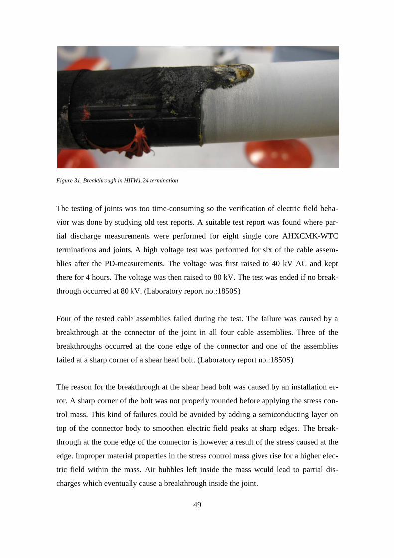
5.2.1 HJW11.2403C
The cable joint examined in this thesis was a HJW11.2403C heat shrink joint. The
product card of the termination describes it as following:
"The joint kit is used for jointing of max. 24 kV cables with XLPE insulation and aluminum shield.
The kit is suitable for AHXAMK-W cables, containing the components for three cores."

30
Figure 14. Content of HJW11.2403C heat shrink joint kit (HJW11.2403C product card)
HJW11.2403C heat shrink joint kit includes following materials:
Medium voltage shear head bolt connector
Stress control tube
Insulating and semiconducting tube
Sealing tube
Stress control tape
Sealing mastic
Gray sealing mastic for screw holes
LV connector
Tinned copper braid
Constant force spring
Self bonding insulating tape
Installation accessory like tape, peeling rope, grinding paper and cleaning tissue.
(HJW11.2403C product card)

31
The key features of installing a HJW11.24 joint are described below, more specific in-
structions can be found in appendix 2.
The structure of a joint consists of two cables prepared as in a termination and a me-
dium voltage connector that connects the cables together. A stress control mass is
stretched on top of the connector body and at the cutting point of the screening in both
cables. The stress control mass smoothen the surface between the connector and the
tube on top of it and prevents air bubbles from being left inside the joint. A shrinkable
two layer stress control tube is shrunk on top of the connector and all the way over the
cutting point of the screening in both cables. The inner layer of the stress control tube is
similar than the stress control tube of a termination but with a slightly lower permittivi-
ty. The outer layer of the stress control tube is insulating. Another tube with insulating
and semi-conductive layers is shrunk on top of the stress control tube. The inner layer of
the second tube is insulating and the outer is semi-conductive. The semi-conductive
layer is used to prevent electric field peaks from generating at the surface of the copper
gauze that is used as a grounding electrode. On top of the copper gauze is a sealing tube
that keeps water out from the joint and provides the mechanical protection that is
needed.

32
6 ELECTRIC FIELD SIMULATION OF MEDIUM VOLTAGE AC-
CESSORY
The aim of the thesis was to optimize the electric field distribution in medium voltage
underground accessory. The optimization was done by changing material properties in
the termination and the joint. Different material setups were compared using COMSOL
Multiphysics to find out the seriousness of each material property.
3D models of a termination and a joint were made to be able to perform the simulations.
The models were made by Peter Kaario from Plasticity with Pro/Engineer. The dimen-
sions for the models were made according to installation instructions. A real termination
and a joint were also built and then cut in half to better represent the shapes inside an
installed product.
The structure in the 3D models was too complex so they could not be used in COMSOL
Multiphysics. COMSOL's personnel proposed to start modeling in 2D mode before
going on with the 3D models. 2D axial symmetry mode was best fitting for the symme-
tric conductors and accessories. The 2D simulations offered enough information for the
study so the 3D models were only used for generating the 2D models.
6.1 Defining the product baseline
The simulations were done in 2D axial symmetry mode. The 2D models were generated
from the 3D files and simplified so that they were axially symmetric. The simplification
only concerned the cable lug in the termination and the connector in the joint. The shape
of the cable lug and the connector was assumed to be symmetric without any screw
holes or screws. The non-symmetric shape of the connector can greatly decrease the du-
rability in the current structure of the joint. The axially symmetric model is drawn from
the center of the conductor outwards to the right side of the Y-axis. A layer of air was
added to the model of the termination to better simulate the real situation. No such layer
is needed in the model of the joint since only the electric field inside the joint is ex-
amined.

33
Figure 15. 2D model of axially symmetric simplified termination
Subdomain settings and boundary conditions need to be specified after importing a
model. The electric properties of all layers or groups are specified in subdomain set-
tings. Conductivity ζ and relative permittivity εr need to be specified for each material
that is used in the simulation.
The conductivity of a material is the inverse of electric resistivity which is a more
commonly specified value for insulating materials. The SI unit for conductivity is sie-
mens per meter (S/m). (Electrical conductivity)
(7)

34
Figure 16. Subdomain settings
Boundary conditions need to be set up after specifying the materials. All boundaries ly-
ing on the Y-axis need to be set as axial symmetry. All internal layers are chosen as
continuity and the outer edges as electric insulation. The conductor is set as electric po-
tential and the aluminum screen of the cable as ground on the X-axis.
Figure 17. Boundary settings
35
After setting up materials and boundaries it is time to generate the mesh for the model.
There are various possibilities when generating a mesh. It is important to always use the
same element net when comparing how changes made in subdomain and boundary set-
tings affect the results.
Figure 18. Meshed model of termination
The final thing to do after generating the mesh is to solve the simulation. The result is
presented as a colored surface model with the electric potential as the default property.
Various post processing tools can be used for analyzing results of different properties. A
line plot is an excellent tool when studying changes in potential difference or electric
field. The line plot tool is used to draw graphs showing how a property changes along a
straight line.

36
6.1.1 Material properties
COMSOL has a material library with some predefined values for basic materials that
can be used in most physic modeling environments. The AC/DC module also comes
with some specific materials that are more commonly used in electronic equipment.
A material library of the materials used in medium voltage cables and accessories had to
be done before the actual simulation could be started. The electric properties used in the
simulations are chosen according to different manufacturer specifications and measure-
ments done by Anssi Aarnio in his Master's Thesis.
The properties for copper, aluminum and air were used from the predefined material
libraries. The conductivity of air was null according to the predefined values. A value of
1e-20 was used to prevent problems in calculations.
Properties for the plastics in cable insulation and screening were obtained from Borealis'
datasheets. The materials are commonly used plastics in medium voltage cables. The
properties for the cable insulation are according to specifications for LE4201R. The
properties for the cable screening are according to Visico™ LE0540 and the cable outer
sheath according to Borstar® HE6062.
Table 1. Electric properties of plastics used in MV cables
Material Volume resistivity [Ωm] Conductivity [σ] Permittivity [εr]
Cable insulation 1.00E+14 1.00E-14 2.3
Cable screening 1.00E+00 1 1
Cable outer sheat 1.00E+14 1.00E-14 2.2
The properties for the tubes and masses used in the termination are according to manu-
facturer specifications. The manufacturer has not specified a relative permittivity for the
non-tracking tube or the sealing mastic so these values were chosen according to the
measurements done by Aarnio. The permittivity values mentioned in Aarnio's thesis are
measured with 140 V at 1000 Hz (Aarnio 2010 p. 69-71). The values used in the simula-
tions are according to measurements done with 140 V at 50 Hz.

37
Table 2. Electric properties of materials used in model of termination
Material Volume resistivity [Ωm] Conductivity [σ] Permittivity [εr]
Non-tracking tube 1.00E+11 1.00E-11 3.4
Stress control tube 1.00E+07 1.00E-07 35
Stress control mastic 1.00E+08 1.00E-08 15
Sealing mastic 1.00E+10 1.00E-10 3.31
Manufacturer specifications were used in the simulation of the joint for all the proper-
ties that had a value specified. The missing values are according to Aarnio's measure-
ments. The stress control tube and the insulating and semiconducting tube are both two-
layer tubes which caused problems in measurements. Aarnio could however identify the
materials used in these layers. The inner layer of the stress control tube is similar as the
stress control tube used in terminations and the outer layer is the same as an insulating
tube. The inner layer of the insulating and semiconducting tube is also the same insulat-
ing tube and the outer layer is same as a semiconducting tube.
Table 3. Electric properties of materials used in model of joint
Material Volume resistivity
[Ωm]
Conductivity
[σ]
Permittivity
[εr]
Stress control mastic 1.00E+08 1.00E-08 15
Stress control tube, inner layer 1.00E+10 1.00E-10 30
Stress control tube, outer layer 1.00E+11 1.00E-11 3.5
Insulating / semiconductive tube,
inner layer 1.00E+10 1.00E-10 3.5
Insulating / semiconductive tube,
outer layer 1.00E+03 1.00E-03 1
Sealing mastic 1.00E+08 1.00E-08 4.26
Sealing tube 1.00E+12 1.00E-12 3

38
6.2 Simulation of a HITW1.24 termination
The point of interest in terms of electric field in a medium voltage termination is the
cutting point of the cable screening. At this point the electric field rises rapidly when the
conductor and the grounding electrode diverge. The structure of a termination at the cut-
ting point can be examined in figure 19. The shining layer on the left is the conductor.
On top of the conductor are the cable insulation and screenings. The yellow layer is the
stress control mass. The cutting point of the insulation screening can be seen inside this
layer. The black layer on top of the mass is the stress control tube and the red layer
above it is the anti-tracking tube.
Figure 19. Cutting point of the cable screening

39
The material properties used in the simulation are according to the values in table 1 and
table 2. The electric potential in the conductor is set as 12 kV. The mesh for the model
was created using default meshing settings with one refining of the mesh. The electric
field strength is displayed on the surface of the model in a color scale and the equipoten-
tial lines as contours. The electric field peak can be seen as a red dot at the cutting point
of the cable screening in figure 19.
Figure 20. Electric field and equipotential lines in HITW1.24 termination
The surface plot illustrates clearly how the stress control mastic and the stress control
tube force the electric field towards the conductor and the stress from the field is mainly
divided within the conductor insulation. When the electric field is controlled like this
the stress at the cutting point of the screening becomes much smaller. The shape of the
electric field can be seen from the equipotential lines. The distance between the lines is
much denser inside the insulation than in the stress control components and therefore
the field is also much higher.
A surface plot with the exactly same element net, but with material properties of the
stress control mastic, stress control tube and the anti-tracking tube changed to air can be

40
used to study the difference between a termination with stress control components and a
bare termination without any sort of grading.
Figure 21. Electric field and equipotential lines in termination without grading
The electric field peak at the cutting point of the cable screening is much higher when
no grading is used. The diverging of the electrodes causes the field to rise remarkably at
the end of the grounded cable screening. The denseness of the equipotential lines at the
cutting point clearly indicates a much higher electric field peak.
The magnitudes of the electric field peaks at the cutting point of the screening can be
examined in figures 22 and 23. Figure 22 illustrate the electric field of a HITW1.24
termination and figure 23 a bare termination without any mass or tubes.

41
Figure 22. Magnitude of electric field in HITW1.24 termination
Figure 23. Magnitude of electric field in termination without grading

42
The graphs are drawn from line plots that start from the center of the conductor and go
straight along the X-axis through the end of the cutting point and continue outwards.
The length of the line is 30 mm and the resolution for the graph is 20000 points along
the line. The unit of the line plot graph is by default V/m but kV/mm is more convenient
when studying the dielectric strength of insulating structures.
The use of a HITW1.24 termination instead of a bare termination decreases the electric
field peak at the cutting point of the screening roughly by 50 %.
6.3 Simulation of a MV cable joint
A medium voltage underground joint differs greatly from a termination in terms of elec-
tric field behavior. The joint is designed to imitate the shape of a cable and the diversion
of electrodes is kept as small as possible.
Electric field peaks are generated at the surface of the connector as a result of sharp cor-
ners. Field peaks are also generated at the cutting points of both cable screenings but
they are not as crucial as in a termination if no air bubbles are left inside the insulating
structures.
The structure of a joint at the connector can be examined in figure 24.The shining layers
on the left are the conductor and the connector. The insulation can be seen above the
conductor in the lower part of the picture. On top of the connector is a layer of yellow
stress control mass. The layer is hard to see since it was damaged while cutting the joint
in half. The black layer on top of the mass is the stress control layer from the stress con-
trol tube. The red layers above it are the insulating layers from both the stress control
tube and the insulating and semi-conductive tube. The black semi conducting layer can
be seen above the red layers. On top of the semi-conducting layer are the copper gauze
and finally the black sealing tube.

43
Figure 24. Connector in a HJW11.24 joint
The material properties used in the simulation are according to the values in table 1 and
table 3. The electric potential in the conductor is set as 12 kV. The model used in the
simulations consists of thin layers that caused problems with meshing. The mesh was
created using free mesh parameters since default settings did not work in this model.
The electric field and potential is displayed in the same way as in the termination. The
field is displayed on the surface in a color scale and equipotential lines are represented
as contours. The electric field peak at the cutting point of the cable screening is not ex-
amined since the behavior is almost the same as in a termination. The peak at the cutting
point is much lower in a joint since the grounding electrode continues on top of the
stress control and insulating tubes. However the stress caused in the insulating struc-
tures above the connector is relatively higher than in other parts of the joint. Peaks in
electric field at this point of the joint can easily lead to failure.

44
Figure 25. Electric field and equipotential lines in a HJW11.24 joint
The surface plot illustrates how the electric field is mainly divided within the insulating
layers of both tubes. The field is also relatively high within the stress control mass and a
peak can clearly be seen at the end of the connector. The highest peak in electric field is
generated within the insulation as a result of the sharp shape used at the cone edge of
the connector.
The magnitude of the electric field within the insulating structures of a HJW11.24 joint
can be examined in figure 26. The graph is drawn from a line plot according to the red
line in figure 27. The line starts inside the connector and goes through the cone edge in
the connector body and through the point of the insulation with the highest peak in elec-
tric field.

45
Figure 26. Electric field in HJW11.2403C joint
Figure 27. Model of line plot used in joint simulations
The length of the line is 14 mm and the resolution for the graph is 20000 points along
the line. The unit of the line plot graph for the joint is also set as kV/mm.

46
7 VERIFICATION OF SIMULATION RESULTS
Measuring the electric field can be extremely hard since the probe used for measure-
ment can disturb the field. The verification of simulation results was decided to be done
by studying the behavior of terminations and joints in high voltage tests. The tests were
performed using a Baur PGK 110 / 5 HB high voltage test set. Basic principle of the test
setup can be seen in figure 27. The conductor was connected to the AC-output and the
aluminum shield to ground.
Termination results were verified by performing a high voltage test where the voltage
was raised with 4 kV steps up to 60 kV AC. The voltage was kept at each level for 1
minute before raising it to the next one. The voltage was kept at 60 kV for 15 minutes
and then dropped down to 48 kV where it was kept for 4 hours. The voltage was finally
raised back to 60 kV where it was kept for at least 30 minutes before ending the test.
Figure 28. Principal high voltage test scheme
Twelve AHXAMK-W terminations were tested in order to verify the electric field de-
fined in the simulations. Six of the terminations were tested without any stress control
components and six with a HITW1.24 termination. Two terminations were tested simul-
taneously on one piece of cable. The bare terminations were tested first and the same
cables were then used for testing the HITW1.24 terminations. The length between the
cutting point of the screening and the connector lug was increased in the bare termina-
tions to prevent flashovers from occurring.

47
Figure 29. Test setup for high voltage test
The behavior of all bare terminations was similar. Surface discharges could be heard
clearly after the 40 kV. Visible slider discharges started to occur at the first 60 kV stage
and the voltage could not be increased higher than this. The surface discharges contin-
ued to occur randomly after dropping the voltage to 48 kV. Loud slider discharges and
flashovers started to occur between the connector lug and the cables screening after rais-
ing the voltage again to 60 kV. Regardless of the discharges none of the samples failed
during the voltage test. Closer examining of the cutting point of the screening showed
that the constant discharges and flashovers at higher voltages had burnt the insulation a
bit. A termination of this type would eventually fail when the insulation would be dam-
aged enough at the cutting point of the screening.

48
Figure 30. Burning marks at cutting point of screening
Both ends of the cables were cut off before installing the HITW1.24 terminations. The
terminations were installed according to the installation instructions. There was no sur-
face discharges or flashovers noticed during the test. One of the HITW1.24 did however
fail after 12 minutes at the first 60 kV stage. The broken termination was cut off and a
new termination was installed on the cable. The new sample passed the whole test with-
out any problems.
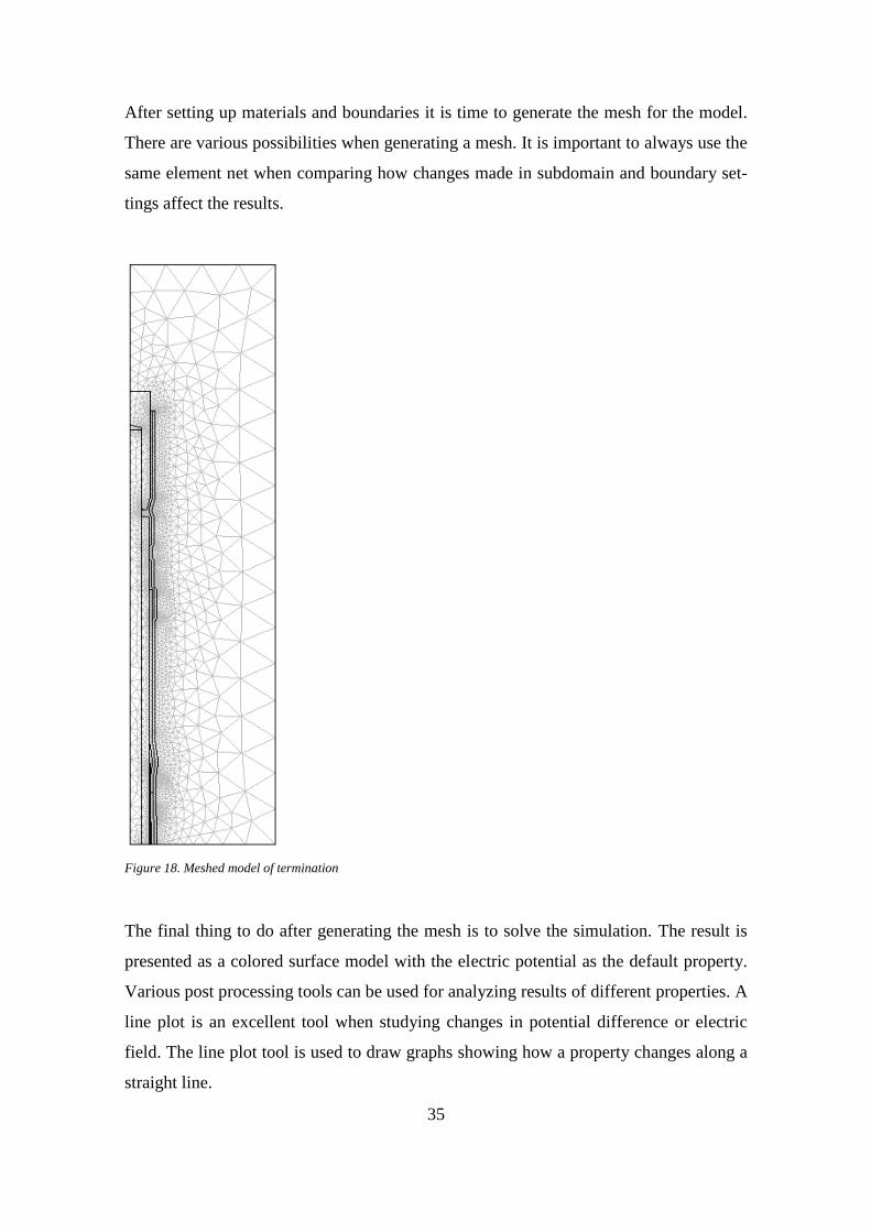
The broken termination was cut open to study the reason for the failure. A breakthrough
had occurred at the cutting point of the screening which caused the insulation to melt
and allowed current to flow between the conductor and the grounded cable screening.
The hole in the insulation was not exactly at the cutting point but instead a bit away
from it. This had probably been the weakest point in the insulation. The reason for the
failure is unknown since no clear installation error could be noticed. Installation errors
are a common reason for failures of this type. The breakthrough could also be a result of
quality issues in the stress control mass or even in the cable insulation. Wrong electric
properties in the mass could lead to a much higher electric field at the cutting point of
the screening. Improper structure of the mass could also lead to a breakthrough if air
bubbles were left inside the termination. Partial discharges generated inside the air bub-
bles would start to slowly burn the insulation and could lead to failure.
49
Figure 31. Breakthrough in HITW1.24 termination
The testing of joints was too time-consuming so the verification of electric field beha-
vior was done by studying old test reports. A suitable test report was found where par-
tial discharge measurements were performed for eight single core AHXCMK-WTC
terminations and joints. A high voltage test was performed for six of the cable assem-
blies after the PD-measurements. The voltage was first raised to 40 kV AC and kept
there for 4 hours. The voltage was then raised to 80 kV. The test was ended if no break-
through occurred at 80 kV. (Laboratory report no.:1850S)
Four of the tested cable assemblies failed during the test. The failure was caused by a
breakthrough at the connector of the joint in all four cable assemblies. Three of the
breakthroughs occurred at the cone edge of the connector and one of the assemblies
failed at a sharp corner of a shear head bolt. (Laboratory report no.:1850S)
The reason for the breakthrough at the shear head bolt was caused by an installation er-
ror. A sharp corner of the bolt was not properly rounded before applying the stress con-
trol mass. This kind of failures could be avoided by adding a semiconducting layer on
top of the connector body to smoothen electric field peaks at sharp edges. The break-
through at the cone edge of the connector is however a result of the stress caused at the
edge. Improper material properties in the stress control mass gives rise for a higher elec-
tric field within the mass. Air bubbles left inside the mass would lead to partial dis-
charges which eventually cause a breakthrough inside the joint.

50
Figure 32. Example of failure at cone edge of connector (Laboratory report no.:1850S)
The high voltage test results clearly show that the cutting point of the cable screening is
the weak point in a termination. All terminations without grading suffered from the high
electric field peak and would eventually have failed with such a high voltage. The
HITW1.24 terminations that passed the test showed no sort of signs of a high electric
peak at the cutting point of the screening. It can thereby be assumed that the grading at
the cutting point of the screening actually works and the electric field peak is decreased
significantly. The failure of a HITW1.24 termination however indicates how important
it is to have correct material properties and to avoid installation errors. Issues like these
can easily make the situation even worse than it is in a termination without any sort of
grading.
The test report indicates that the weakest point of a cable joint is the cone edge of the
connector. The material properties of the stress control mass play a key role in the dura-
bility of a cable joint of this type.
The high voltage results and the test report both support the electric field behavior of the
simulations. The simulation software can thereby be used as an indicative tool to im-
prove the electric field in medium voltage accessories.

51
8 PRODUCT OPTIMIZATION
The product optimization was done by modifying material properties in the models. No
changes were made to the original structure of the termination and joint. The properties
for insulating materials are generally quite equal but a wide variety of different stress
control components are available. Because of this the optimization was done by study-
ing how different stress control materials affect the electric field behavior. The aim was
to find out an optimal solution for the current structure of terminations and joints.
Different manufacturers offer a variety of stress control masses with relative permittivi-
ties between approximately 10 and 20. The conductivities of the masses are generally
between 1e-8 and 1e-12. The properties of tubes also vary greatly as relative permittivi-
ties go from about 20 to 40 and conductivity from 1e-7 to 1e-13.
The affect of permittivity and conductivity were studied separately. The lowest and
highest possible permittivity was simulated with a fixed conductivity value. The lowest
and highest possible conductivity was then simulated with a fixed permittivity value.
The fixed value was chosen so that it was in the middle of the lowest and highest value.
This kind of an approach offers eight different solutions for the termination and the joint
and gives a good idea of an optimal solution. The material properties used in each simu-
lation setup can be seen in table 4.

52
Table 4. Simulation setups
Stress control mass Stress control tube
Simulation
setup
Permittivity
[εr]
Conductivity
[σ]
Permittivity
[εr]
Conductivity
[σ]
1 10 1.00E-10 20 1.00E-10
2 10 1.00E-10 40 1.00E-10
3 20 1.00E-10 20 1.00E-10
4 20 1.00E-10 40 1.00E-10
5 15 1.00E-08 30 1.00E-07
6 15 1.00E-08 30 1.00E-13
7 15 1.00E-12 30 1.00E-07
8 15 1.00E-12 30 1.00E-13
The material properties for the cable insulation and screening are according to table 1 in
all simulations setups. The material properties for all insulating layers and the semi-
conductive layer in the joint are according to table 5 in all simulation setups.
Table 5. Electric properties of insulating and semi-conductive layers used in simulations
Material Conductivity [σ] Permittivity [εr]
Insulating layers 1.00E-11 3.5
Semi-conducting layer 1.00E-03 1
All simulations were done using the same boundary and mesh setting as described in
chapter 6. The setting for the line plot used for measuring the electric field was also the
same as in chapter 6. The simulation results for the termination can be seen in table 6.
The "Field peak" in the table indicates the peak value at the cutting point of the screen-
ing between the cable insulation and stress control mass.
The results indicate that using a higher permittivity for both the mass and the tube is
better. For conductivity the situation is similar, higher conductivity leads to a lower
electric field peak. It is clearly seen from the simulation results that the permittivity af-
fects the result more than conductivity does. The permittivity of the mass has a higher

53
impact on the resulting peak. The highest permittivity for the mass and the tube in setup
3 results in about 25 % lower electric field peak at the cutting point of the screening
than it would be with the lowest permittivity values in setup 1.
The conductivity of materials does not affect the electric field peak greatly. The highest
conductivity for the mass and tube in setup 5 only results in about 3 % lower electric
field peak at the cutting point of the screening than it would be with the lowest conduc-
tivity values in setup 8.
Table 6. Field peak results for terminations
Simulation
setup
Field peak
[kV/mm]
Simulation
setup
Field peak
[kV/mm]
1 5.45
5 4.5
2 5.3
6 4.6
3 4.15
7 4.55
4 4.05
8 4.65
Combining the permittivities from setup 4 and the conductivities from setup 5 results in
an electric field peak of 4 kV/mm. The combination of permittivities from setup 1 and
conductivities from setup 8 results in an electric field peak of 5.5 kV/mm. When no
grading at all is used the resulting electric field peak is approximately 9 kV/mm.
The difference between the best and the worst setup is significant. The use of the high-
est permittivities and conductivities leads to about 55 % lower electric field peak than
without any grading. The lowest permittivities and conductivities lead to about 39 %
lower electric field peak than without any grading.
The structure of the joint results in a bit more complicated field than in that of a termi-
nation. The resulting line graph shows two peaks in the electric field at the cone edge of
the connector. The first peak is at the surface between the connector and the stress con-
trol mass and the second is at the surface between the stress control tube and the insulat-
ing layers. The second peak between the stress control layer and the insulating layer is

54
much higher than the one at the connector surface. This peak is generated between two
layers of a two layer tube and the bond can be assumed to be of extremely good quality.
Because of this we can assume that this is not the most critical point. The peak at the
connector surface seems to be more important regarding the durability of a joint.
The simulation results for the joint can be seen in table 7. The first value in "Field peak"
column is the peak at the surface of the connector and the second is the peak inside the
stress control tube. The results for the joint also indicate that permittivity affects the re-
sulting electric field more than conductivity does. The best combination is however not
with the highest possible permittivity for the mass and the tube in setup 4. A high per-
mittivity mass and a low permittivity tube in setup 3 results in a slightly lower peak at
the surface of the connector.
The changes in conductivity are almost insignificant to the resulting electric field. A
high conductivity mass and a low conductivity tube in setup 6 seem to be slightly better
than other combinations.
Table 7. Field peak results for joints
Simulation
setup
Field peak
[kV/mm]
Simulation
setup
Field peak
[kV/mm]
1 1.25 / 2.7
5 0.8 / 2.95
2 1.3 / 2.8
6 0.8 / 2.85
3 0.65 / 2.85
7 0.85 / 2.95
4 0.7 / 2.95
8 0.85 / 2.85
The use of a high permittivity mass leads to roughly about 50 % lower electric field
peak at the surface of the connector than with low permittivity. The permittivity of the
tube does not affect the electric field at the surface of the connector by much in a cable
joint of this type. The use of a stress control tube at this point of the joint seems point-
less and is more likely used for ease of installation.

55
The performance of a joint could be improved by adding a semi-conducting layer on top
of the connector before applying the stress control mass. The semi-conducting layer
would smooth the surface and therefore prevent electric field peaks from being generat-
ed. The use of a semi-conducting mass or tube could possibly replace the stress control
mass completely above the conductor.

56
9 CONCLUSION
The aim for the thesis was to study how relative permittivity and volume resistivity of
stress control components affected the electric field in a medium voltage underground
termination and joint.
Material properties of the stress control components play a key role in the durability of a
termination or a joint. The results indicate that permittivity has a much higher effect on
the resulting electric field than volume resistivity has. It should be noted that the permit-
tivity is not a constant in reality, as it was assumed in the simulations.
The electric field peaks are relatively low with the 12 kV voltages that were used in the
simulations. It is however important to note that all simulations represent ideal insula-
tors without any air bubbles or dirt between layers. In reality no insulator is ideal and
microscopic air bubbles exists in all layers. Therefore the resulting electric field is al-
ways higher than that represented in simulations.
The literature study and the simulations revealed that the current structure of the joint
could be improved. Adding a semi-conductive layer on top of the connector would de-
crease the faults caused by installation errors but the ease of installation would possibly
suffer.
The simulation of electric field offers great potential when comparing material proper-
ties of insulating structures. Structural changes could also be examined but it in this case
it is important to have a small enough element net to get reliable results. Adding more
physical conditions like heating to simulations could be a subject for future research.
The stress control materials always have some sort of loss factor that affects the perfor-
mance of these materials.
Only basic functions of COMSOL Multiphysics were used in this thesis. The software
offers a lot of functions and specified options that were not used at all. The version of
COMSOL Multiphysics that was used is 3.5a. A newer 4.0 version was released during
the making of this thesis. The newer version offers more functions and new physical

57
modeling environments. The support for different file types is also improved in the new
version.
The 3D file suitability with pro/engineer files was disappointing at first. The expectation
was to use relatively big 3D models of the complete products in simulations. There were
also problems with the 2D file conversions in the beginning. These problems were
solved once the correct settings were found. The issues with the 3D models were never
completely solved but smaller parts of the models could be simulated with the help of
COMSOL's personnel. The source for the problems was related to the complexness of
the models and errors that occurred in the conversion between different file formats.
Regardless of the issues, my general opinion of COMSOL Multiphysics is positive. The
approach to use 3D models in the thesis was not the best possible and it is something I
would not do again if I should start with a similar project. The software is easy to use
and offers a lot of functions and usability for product development purposes.
Besides product development software like COMSOL Multiphysics offer great utiliza-
tion for other purposes. Elegant visual field plots could for example be used in training
and sales to gives a better picture of the company for outside persons.

58
REFERENCES
Aarnio, Anssi. 2010, Characterization of non-metallic materials for medium voltage
cable accessories, Master's thesis, Tampere: University of Technology, Material
Science.
AC/DC Module. COMSOL Multiphysics. [Cited: 15.8.2010] Available at:
http://www.comsol.fi/products/acdc/
Aro, Martti; Elovaara, Jarmo; Karttunen, Matti; Nousiainen, Kirsi & Palva, Veikko.
2003, Suurjännitetekniikka, 2nd ed., Otatieto, 520 p.
Borstar® HE6062 datasheet, 9.7.2010, 2nd ed., Borealis. [Cited: 28.10.2010] Available
at: http://www.borealisgroup.com/datasheets/10025446
CAD Import Module. COMSOL Multiphysics. [Cited: 15.8.2010] Available at:
http://www.comsol.fi/products/cad-import/
COMSOL Multiphysics. [Cited 15.8.2010] Available at:
http://www.comsol.fi/products/multiphysics/
Electrical conductivity, Wikipedia. [Cited: 28.10.2010] Available at:
http://en.wikipedia.org/wiki/Electrical_conductivity
Elovaara, Jarmo & Laiho, Yrjö. 1988, Sähkölaitostekniikan perusteet, 2nd ed., Otakus-
tantamo, 487 p.
Hirvonen, Markus. 2008, Effect of assembly error on partial discharge levels in medium
voltage terminations, Engineering thesis, Helsinki: Stadia, Power Systems.
HITW1.2403L product card. Ensto Finland Oy. [Cited: 16.9.2010] Available at:
http://products.ensto.com/catalog/11051/product/15771/HITW1.2403L_ENG1.html
HJW11.2403C product card. Ensto Finland Oy.. [Cited: 16.9.2010] Available at:
http://products.ensto.com/catalog/11041/product/15853/HJW11.2403C_ENG1.html
Laboratory report no.:1850S, 9.4.2010, Ensto UN Laboratory.
LE4201R datasheet, Borealis. [Cited: 16.9.2010] Available at:
http://www.borealisgroup.com/datasheets/10024590
Obituary: Germund Dahlquist. 1.5.2005, Society for Industrial and Applied
Mathematics. [Cited: 15.8.2010] Available at:
http://www.siam.org/news/news.php?id=54

59
Reka kaapeli OY. DRYREX Korkealaatuiset keskijännitekaapelit. [Cited: 16.9.2010]
Available at:
http://www.reka.fi/files/965_Korkealaatuisetkeskijnnitekaapelit.pdf
Training Module: Ensto Underground Solutions, Ensto Utility Networks.
[Cited: 28.10.2010].
Visico™ LE0540 datasheet, 19.11.2009, 15th ed., Borealis. [Cited: 28.10.2010]
Available at: http://www.borealisgroup.com/datasheets/10011400
Wolfson, Richard. 2007, Essential university physics, Pearson Education Inc.,
728 p.

APPENDICES
1. HITW1.24 Installation instructions
2. HJW11.24 Installation instructions

INSTALLATION INSTRUCTION PEM1074ENG2008-08
Eesti
ENGLISH
HEAT SHRINK INDOOR TERMINATIONS HITW1.24HEAT SHRINK OUTDOOR TERMINATIONS HOTW1.24

2/12 HITW1 AND HOTW1 PEM1074ENG 2008-08
GENERAL INFORMATION- Check that the kit is suitable for the cable type.
- Check the materials listed in the bill of materials for completeness.
- Read the installation instructions carefully before starting the installation.
- Install carefully and make sure the materials are clean during the installation.
- Clean the working place after the installation.
GENERAL INSTRUCTONS FOR HEAT SHRINKING- Please note that in some working places a hot work licence is needed.
- Use a propane burner with a flame length of approx. 20-30 cm. Do not use too large or sharp flame.
- Move the flame all around the cable on the shrinking direction. Move the flame continuously to avoid over-
heating.
- Make sure that the ventilation is good and there are no flammable materials around.
- Clean the cable surfaces before shrinking.
- When shrinking, always follow the installation instructions and the relevant sequence to avoid trapped air.
- Check that the tube has shrunk evenly around the cable before you continue shrinking.
- If the tube turns around at the end of shrinking, straighten the tube by directing the flame inside the tube
from the opposite direction.
- After shrinking the tubes should be smooth and even following the shape inside.
LEGAL NOTICE- The product must be installed only by a competent person with sufficient training in installation practices
and with sufficient knowledge of good safety and installation practices in respect of electrical equipment.
If local legislation contains provisions in respect of such training or sufficient knowledge in respect of
installation of electrical equipment such provisions shall be fulfilled by the said person.
- Ensto accepts no liability concerning claims resulting from misuse, incorrect installation or ignored na-
tional safety regulations or other national provisions.
- WARNING: Failure to follow the installation instructions may result in damage to the product and serious
or fatal injury.

PEM1074ENG 2008-08 HITW1 AND HOTW1 3/12
1. Check the length of each core according to the final installed position.
2. Mark the cutting point at the distance of 310 mm from the core end.
3. Heat the outer sheath up to the mark.
Reference line
Outer sheath
Surplus part
Mark
310
Outer sheath

4/12 HITW1 AND HOTW1 PEM1074ENG 2008-08
4. Use the peeling rope to remove the outer sheath to leave the aluminium foil exposed. Heat the aluminium foil close to the outer sheath with gentle flame. Remove the most of the adhesive coating from the aluminium tape for up to 40 mm from the outer sheath by the help of the peeling rope. Use the grinding paper included in the kit to remove rest of the adhesive coating from the aluminium foil up to 40 mm from the outer sheath. Take care that the aluminium tape does not break during the grinding.
5. Install the constant force spring 40 mm away from the end of the outer sheath. Remove the alu-minium foil by tearing it against the constant force spring.
6. Move the spring a little towards the core so that the aluminium foil edge remains under the spring. Tear the swelling tape in longitudal strips up to the spring. Remove the tape strips by tearing them against the spring. Remove the constant force spring.
7. Remove the semiconductive layer leaving 40 mm measured from the Al foil. Use a suitable tool. If necessary, remove any remaining of the semiconductive layer with a piece of glass. Use the grinding paper included in the kit to smooth the insulation. Remove the insulation for the length equivalent to the bolt cable lug depth + 5 mm. If you use compression lugs, remove the insula-tion following the lug manufacturer’s instructions. Be careful not to nick the conductor. Clean the conductor.
Peeling rope
310Mark
Outer sheath Aluminium foil
40
Constant force spring
Insulation
Aluminium foil
Conductor
Lug depth + 5
Semiconductive layer
Aluminium foil
Aluminium foil
40
Outer sheath Semiconductive layer
40

PEM1074ENG 2008-08 HITW1 AND HOTW1 5/12
8. I nstall a suitable cable lug following the manufacturer’s instructions. Remember to orient it cor-rectly and to remove any sharp edges. Fill the holes with grey mastic.
9. Clean the cable insulation with a cleaning tissue. Go towards the semiconductive layer, and finally clean the semiconductive layer without touching the insulation. Thus no semiconductive particles are deposited on the insulation.
10. Wrap two layers of stress control tape SSCTA85 over the edge of the semiconductive layer. Wrap the tape for 10 mm on the semiconductive layer and 20 mm on the insulation. Start from the sem-iconductive layer. Stress control tape SSCTA85 must be wrapped with a 50 % overlap by stretching it to half of its original width.
SSCT
11. Place the stress control tube SSCT so that it overlaps 10 mm of the semiconductive layer. Start shrinking of the stress control tube from the end located on the semiconductive layer and contin-ue towards the other end. Wrap one layer of sealing mastic SSM83 for 40 mm length on the outer sheath. Sealing mastic SSM83 must be wrapped by stretching it a bit.
MV cable lug
Conductor
Insulation
Outer sheath
Stress control tape SSCTA85
Grey mastic
10 20
MV cable lug
Outer sheath
Sealing mastic SSM83
Semiconductive layer
Stress control tube SSCT
40 10

6/12 HITW1 AND HOTW1 PEM1074ENG 2008-08
SSCT
12. Place the end of the ground copper braid closest to the tinned zone (water block) on top of the exposed aluminium foil and fix the ground copper braid on the top of the aluminium foil with one turn of the constant force spring.
SSCT
13. Fold the ground copper braid over the constant force spring so that the tinned zone remains on the sealing mastic.
SSCT
14. Wrap the rest of the constant force spring around the cable.
SSCT
15. Wrap some layers of self-bonding insulating tape SSITA42 on the constant force spring and on the exposed aluminium foil to smooth the sharp edges. Self-bonding insulating tape must be wrapped by stretching it a bit. Wrap the tape to the direction, which tightens up the constant force spring.
SSCT
16. Fill the gaps between the ground copper braid tinned zone and the outer sheath with some seal-ing mastic SSM83. Then wrap one layer of the same mastic to cover the ground copper braid tinned zone area and the constant force spring area up to the edge of the SSCT stress control tube. Sealing mastic SSM83 must be applied by stretching it a bit. Wrap one layer of sealing mas-tic SSM83 by stretching it a bit around the other end of the SSCT stress control tube to fill and smooth the transition between the tube and the insulation.
Tinned zone
Constant force spring
Ground copper braid
Tinned zone
Constant force springGround
copper braid
Outer sheath Constant force spring
Outer sheath
Insulation
Semiconductive layer
Self-bonding insulating tape SSITA42
Ground copper braid
Sealing mastic SSM83
Tinned zone
Stress control tube SSCT
Sealing mastic SSM83

PEM1074ENG 2008-08 HITW1 AND HOTW1 7/12
SSCT
17. Fill the gap between the end of the cable lug and the insulation with sealing mastic SSM83. Then apply two layers of sealing mastic SSM83 to cover 20 mm of insulation and the barrel of the cable lug. The sealing mastic must be applied by stretching it a bit.
SSCTSAT
18. Place the SAT nontracking tube so that it covers the cable lug barrel completely. Shrink the tube starting from the cable sheath end.
24 kV INDOOR TERMINATION HITW1.24
SAT
19. Place the rain shed so that the shed neck edge is at 200 mm from the the nontracking tube end. Shrink the rain shed directing the heat only to its neck.
SAT
20. Indoor termination HITW1.24 is finished and ready to use!
Rain shed
Nontracking tube- SAT -
200
Sealing mastic SSM83
20

8/12 HITW1 AND HOTW1 PEM1074ENG 2008-08
24 kV OUTDOOR TERMINATION HOTW1.24
SAT
21. Place the rain shed so that the shed neck edge is at 200 mm from the nontracking tube end. Shrink the rain shed directing the heat only to its neck. Shrink the other two rain sheds so that they are spaced 60 mm.
SAT
22. Outdoor termination HOTW1.24 is finished and ready to use!
23. Install the LV cable lug included in the kit on the separate earthing conductor of the cable.
Rain shed(second)
200
60 60
Rain shed(first) Rain shed
(third)

Um kV b min mm c min mm
12 15 10
17,5 20 15
24 25 20
36 30 25
a = according to local requirements
60 6060 6060 60
a
b
45º
c
20 x D
Dmin


ENSTO SEKKO OYP.O.BOX 5106101 PORVOO, FINLANDTEL. +358 204 76 21FAX. +358 204 76 [email protected]
WWW.ENSTO.COM
PEM
1074
ENG
/ Iss
ue 2
008-
08-2
9
UTILITY NETWORKS

INSTALLATION INSTRUCTION PEM1068ENG2009-12
ENGLISHHEAT SHRINK JOINTS HJW11.24

2/12 HJW11.24 PEM1068ENG 2009-12
GENERAL INFORMATION- Check that the kit is suitable for the cable type.
- Check the materials listed in the bill of materials for completeness.
- Read the installation instructions carefully before starting the installation.
- I nstall carefully and make sure the materials are clean during the installation.
- Clean the working place after the installation.
GENERAL INSTRUCTIONS FOR HEAT SHRINKING- Please note that in some working places a hot work permit is needed.
- Use a propane burner with a flame length of approx. 20-30 cm. Do not use too large or sharp flame.
- Move the flame all around the cable on the shrinking direction. Move the flame continuously to avoid over-
heating.
- Make sure that the ventilation is good and there are no flammable materials around.
- Clean the cable surfaces before shrinking.
- When shrinking, always follow the installation instructions and the relevant sequence to avoid trapped air.
- Check that the tube has shrunk evenly around the cable before you continue shrinking.
- If the tube turns around at the end of shrinking, straighten the tube by directing the flame inside the tube
from the opposite direction.
- After shrinking the tubes should be smooth and even following the shape inside.
LEGAL NOTICE- The product must be installed only by a competent person with sufficient training in installation practices
and with sufficient knowledge of good safety and installation practices in respect of electrical equipment.
If local legislation contains provisions in respect of such training or sufficient knowledge in respect of
installation of electrical equipment such provisions shall be fulfilled by the said person.
- Ensto accepts no liability concerning claims resulting from misuse, incorrect installation or ignored na-
tional safety regulations or other national provisions.
- WARNING: Failure to follow the installation instructions may result in damage to the product and serious
or fatal injury.

PEM1068ENG 2009-12 HJW11.24 3/12
1. Check the length of each core according to the final installed position.
2. Mark the cutting point at the distance A from the core end.
Table 1
CABLE PREPARATION DIMENSIONS
Kit UmkV
Cable sizemm²
Outer sheath removal A mm
Max. connector dimensions
length mm diameter mm
HJW11.2402 24 25-95 280 90 25
HJW11.2403 24 95-240 300 130 33
HJW11.2404 24 150-300 330 180 38
Mark
Reference line
Outer sheath
Surplus part
A
Surplus part

4/12 HJW11.24 PEM1068ENG 2009-12
3. Heat the outer sheath up to the mark.
4. Use the peeling rope to remove the outer sheath to leave the aluminium foil exposed. Heat the aluminium foil close to the outer sheath with gentle flame. Remove the most of the adhesive coating from the aluminium tape for up to 40 mm from the outer sheath by the help of the peeling rope.
Use the grinding paper included in the kit to remove rest of the adhesive coating from the alu-minium foil up to 40 mm from the outer sheath. Take care that the aluminium tape does not break during the grinding.
5. Install the constant force spring 40 mm away from the end of the outer sheath. Remove the alu-minium foil by tearing it against the constant force spring.
Peeling rope
40
40
Outer sheath
Constant force spring
Aluminium foil
Mark A
Outer sheath
Aluminium foil
PEM1068ENG 2009-12 HJW11.24 5/12
6. Move the spring a little towards the core so that the aluminium foil edge remains under the spring. Tear the swelling tape in longitudal strips up to the spring. Remove the tape strips by tearing them against the spring. Remove the constant force spring.
7. Remove the semiconductive layer leaving 80 mm measured from the aluminium foil. Use a suit-able tool. If necessary, remove any remaining of the semiconductive layer with a piece of glass. Use the grinding paper included in the kit to smooth the insulation.
8. Remove half of the bolt connector length + 5 mm from the insulation of the cable. If you use com-pression connectors, remove the insulation following the connector manufacturer’s instructions. Be careful not to nick the conductor. Clean the conductors and wrap a couple layers of PVC tape on the ends of the conductor.
SISCT
CPEEPL SIST
9. Slip the stress control tube SISCT, the insulating / semiconductive tube SIST and the sealing tube CPEEPL on the cables.
Semiconductive layer Insulation
80
Insulation Conductor
Half connector + 5 Half connector + 5
Insulation
Sealing tube CPEEPLGround copper braid (tubular) Stress control tube SISCT
Insulating / semiconductive tube SIST
Aluminium foil Semiconductive layer

6/12 HJW11.24 PEM1068ENG 2009-12
10. Remove the PVC tape from the ends of the conductors and install a suitable connector following manufacturer’s instructions. Remove any sharp edges. Fill the holes left in the connector with grey mastic.
11. Clean the cable insulation with a cleaning tissue. Go towards the semiconductive layer and finally clean the semiconductive layer without touching the insulation, thus no semiconductive particles are deposited on the insulation. Clean the connector.
12. Fill the gap between the end of the connector and the insulation with stress control tape SSCTA85. Then apply two layers of stress control tape SSCTA85 to cover the connector. Continue
up to 15 mm on the insulation on either side. Stress control tape SSCTA85 must be wrapped with a 50 % overlap and by stretching it to half of its original width.
Wrap two layers of stress control tape SSCTA85 over the semiconductive layer edge. Wrap stress control tape SSCTA85 on 10 mm of the semiconductive layer and 20 mm on the insulation. Start from the semiconductive layer. Stress control tape SSCTA85 must be wrapped with a 50% overlap and by stretching it to half of its original width.
Stress control tape SSCTA85
10 20 15 15 20 10
Stress control tape SSCTA85 Stress control tape SSCTA85
Grey masticClean the insulation Clean the insulation
Cleaning directionCleaning direction
MV connector

PEM1068ENG 2009-12 HJW11.24 7/12
SISCT
13. Centre the SISCT stress control tube on the connector. Ensure that the stress control tube over-laps the semiconductive layer on both sides of the joint. Start shrinking the tube from the middle and move towards the ends. Clean the surface of the stress control tube with a cleaning tissue after shrinking.
SISCT
14. Fill the gap between the aluminium foil and the stress control tube by two layers of sealing mas-tic SSM75 on both sides of the joint.
SIST
SISCT
15. Centre the SIST heat shrinkable insulating / semiconductive tube on top of the stress control tube. Start shrinking it from the middle and move towards the ends.
16. Centre the tubular ground copper braid on the joint.
Semiconductive layer Stress control tube SISCT
Shrinking sequence
Semiconductive layer
Sealing mastic SSM75 Sealing mastic SSM75
Insulating / semiconductive tube SIST
Ground copper braid (tubular)
Shrinking sequence

8/12 HJW11.24 PEM1068ENG 2009-12
17. If necessary, fix the braid temporarily with some PVC tape. Fix the other end of the braid with two turns of the constant force spring. Fold the braid end over the spring, and turn the rest of the spring on the braid. Draw the braid to the other side of the joint so that it fits tight on the joint, and fix its end the similar way as the other end.
18. Wrap sone layers of self-bonding insulating tape SSITA42 on the constant force springs and the ground copper braid wires to smooth the sharp edges. Take care that the ends of the braid wires are fully embedded in the taping. Self bonding insulating tape must be wrapped by stretching it a bit. Wrap the tape to the direction, which tightens up the constant force spring.
19. Roughen around 100 mm of the outer sheath on both sides of the joint with grinding paper. Treat the roughened parts gently with flame. Cover the exposed aluminium tape with some layers of sealing mastic SSM75.
CPEEPL
20. Centre the CPEEPL sealing tube on the joint. Start shrinking the tube from the middle and move towards the ends. The tube is properly shrunk when the adhesive starts coming out from the ends.
Constant force spring Constant force spring
Self bonding insulating tape SSITA42
Roughen Sealing mastic SSM75 Sealing mastic SSM75
100 100
Roughen
Sealing tube CPEEPL
Shrinking sequence

PEM1068ENG 2009-12 HJW11.24 9/12
21. The joint is finished and ready to use, but let it cool down before loading it mechanically.
22. Join the separate earthing conductor of the cable with the LV connector included in the kit.

10/12 NOTES PEM1068ENG 2009-12

PEM1068ENG 2009-12 NOTES 11/12

ENSTO SEKKO OYP.O.BOX 5106101 PORVOO, FINLANDTEL. +358 204 76 21FAX. +358 204 76 [email protected]
WWW.ENSTO.COM
PEM
1068
ENG
/ Iss
ue 2
009-
12-2
3
UTILITY NETWORKS