Embed Size (px)
Citation preview
1416 IEEE TRANSACTIONS ON ELECTRON DEVICES, VOL. 51, NO. 9, SEPTEMBER 2004
The Effect of LAC Doping on Deep SubmicrometerTransistor Capacitances and its Influence on
Device RF PerformanceK. Narasimhulu, Student Member, IEEE, Madhav P. Desai, Member, IEEE, Siva G. Narendra, and
V. Ramgopal Rao, Senior Member, IEEE
Abstract—In this paper, we have systematically investigated theeffect of lateral asymmetric doping on the MOS transistor capaci-tances and compared their values with conventional (CON) MOS-FETs. Our results show that, in lateral asymmetric channel (LAC)MOSFETs, there is nearly a 10% total gate capacitance reductionin the saturation region at the 100-nm technology node. We alsoshow that this reduction in the gate capacitance contributes towardimprovement in , max, and RF current gain, along with an im-proved transconductance in these devices. Our results also showthat reduced short-channel effects in LAC devices improve the RFpower gain. Finally, we report that the lateral asymmetric channeldoping gives rise to a lower drain voltage noise spectral densitycompared to CON devices, due to the more uniform electric fieldand electron velocity distributions in the channel.
Index Terms—Analog, drain voltage noise spectral densities, lat-eral asymmetric channel (LAC), RF CMOS.
I. INTRODUCTION
OVER A PERIOD of twenty years, CMOS devices havebeen scaled down to the sub-100-nm regime based on
the electric field scaling principles. This continuous scaling ofthe transistor dimensions has made silicon CMOS technologyviable for high-performance logic and memory applications.Also, with scaling of the device dimensions into the sub-100-nmregime, the transistors have achieved cutoff frequencies in therange of several GHz, making CMOS technology suitable forwireless communications and other RF applications [1]–[7].However, undesirable short-channel effects, the mobilitydegradation and increased parasitic capacitances drasticallyreduce the device transconductance, voltage gains and noiseperformance making the scaled technologies unsuitable foranalog/RF applications [8]–[11].
In order to overcome the above mentioned undesirableeffects, quite a few researchers have looked at lateral asym-metric channel (LAC) or single halo (SH) devices for highperformance analog and mixed signal applications [12]–[19].However, a complete understanding of transistor capacitancesand the RF performance tradeoffs in these MOSFETs is re-quired for device optimization for system-on-chip applications.
Manuscript received January 19, 2004; revised April 29, 2004. The review ofthe paper was arranged by Editor R. Singh.
K. Narasimhulu, M. P. Desai, and V. R. Rao are with the Department of Elec-trical Engineering, Indian Institute of Technology, Bombay, Powai, Mumbai-4000076, India (e-mail: [email protected]).
S. G. Narendra is with the Microprocessor Research Laboratory, Intel Corpo-ration, Hillsboro, OR 97124 USA.
Digital Object Identifier 10.1109/TED.2004.833589
This work, for the first time, analyzes the capacitances inasymmetrically doped MOSFETs and evaluates the perfor-mance tradeoffs with these technologies in the RF regimewith extensive process, and device simulations. The results arecompared with conventional (CON) CMOS technologies. InSection II, we discuss the simulation details while the devicecapacitances in aggressively scaled LAC MOSFETs are dis-cussed in Section III. The effect of lateral asymmetric channeldoping on the device RF performance is explored in Section IV.Simulation results on the device noise are reported in Sec-tion IV-C and correlated with the asymmetric channel dopingpresent in these MOSFETs. Finally, Section V concludes thiswork summarizing the important findings.
II. SIMULATION SETUP
In this section, the simulation structures of LAC and CONMOS transistors are discussed. The process flow for LAC MOS-FETs is identical to that of conventional MOSFETs except forthe threshold adjust implant, which is done through a tilted angleimplantation from the source side, after the gate electrode for-mation [16]. Pocket implant parameters such as dose, energy,and tilt angle are optimized in order to maximize the device per-formance parameters. These optimized devices are used for esti-mating the RF performance trends in Section IV. All the two-di-mensional (2-D) simulations have been carried out using ISETCAD. DIOS process simulator was used for simulating the de-vice structure; MDRAW tool is used for making the simulationgrids and DESSIS tool is used for device simulations [20]. En-ergy balance models are used for device simulations in order toaccount for the nonlocal effects. In order to take surface quanti-zation effects into account, Van–Dorts model is used for devicesimulations. The device models and their constants are adjustedto match the device experimental data down to 200 nm. For theLAC MOSFETs used in simulations, the pocket has been real-ized (boron for n-MOSFETs and arsenic for p-MOSFETs) at atilt angle implantation of 7 . The standard threshold adjust im-plant has been done with BF for CON devices. For both CONand LAC devices, the implantation dose is adjusted to achievean identical of 0.2 V.
III. DEVICE CAPACITANCES
In this section, the effect of LAC doping on MOS transistorcapacitances is discussed. Unless otherwise specified, for all thecomparison studies involving CON and LAC MOSFETs, the
0018-9383/04$20.00 © 2004 IEEE
NARASIMHULU et al.: EFFECT OF LAC DOPING ON DEEP SUBMICROMETER TRANSISTOR CAPACITANCES 1417
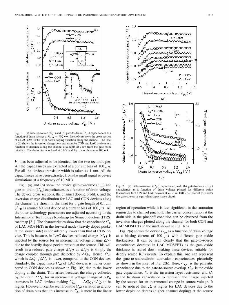
Fig. 1. (a) Gate-to-source (C ) and (b) gate-to-drain (C ) capacitances as afunction of drain voltage at I = 100�A. Inset of (a) shows the cross sectionof a LAC nMOSFET with boron doping variation along the channel. The insetin (b) shows the inversion charge concentration for CON and LAC devices as afunction of distance along the channel at a depth of 2 nm from the gate oxideinterface. The drain bias was fixed at 0.6 V and I was chosen as 100 �A.
has been adjusted to be identical for the two technologies.All the capacitances are extracted at a current bias of 100 .For all the devices transistor width is taken as 1 m. All thecapacitances have been extracted from the small signal ac devicesimulations at a frequency of 10 MHz.
Fig. 1(a) and (b) show the device gate-to-source ( ) andgate-to-drain ( ) capacitances as a function of drain voltage.The device cross sections, the channel doping profiles, and theinversion charge distribution for LAC and CON devices alongthe channel are shown in the inset for a gate length of 0.1 m( is around 80 nm) device at a current bias of 100 . Allthe other technology parameters are adjusted according to theInternational Technology Roadmap for Semiconductors (ITRS)roadmap [21]. The characteristics show that the capacitanceof LAC MOSFETs in the forward mode (heavily doped pocketat the source side) is considerably lower than that of CON de-vice. This is because, in LAC devices reduced charge isinjected by the source for an incremental voltage changedue to the heavily doped pocket present at the source. This willresult in a reduced gate charge as is simply thecharge coupled through gate dielectric by . Hence, ,which is is lower, compared to the CON devices.Similarly, the capacitance of LAC devices is higher com-pared to CON devices as shown in Fig. 1(b) due to the lowerdoping at the drain. This arises because, the charge collectedby the drain for an incremental voltage change ofincreases in LAC devices making to behigher. However, it can be seen from the variation as a func-tion of drain bias that, this increase in is more in the linear
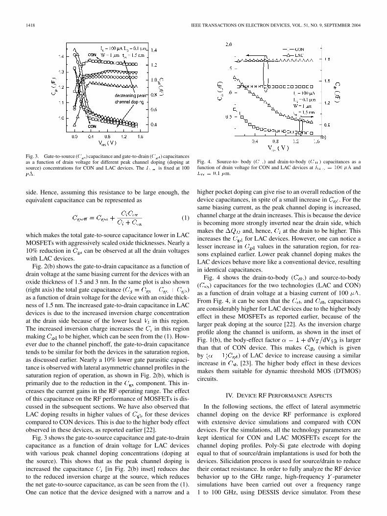
Fig. 2. (a) Gate-to-source (C ) capacitance and, (b) gate-to-drain (C )capacitance as a function of drain voltage plotted for different oxidethicknesses for CON and LAC devices at I = 100 �A. Inset of (b) showsthe gate-to-source equivalent capacitance circuit.
region of operation while it is less significant in the saturationregion due to channel pinchoff. The carrier concentration at thedrain side in the pinchoff condition can be observed from theinversion charges plotted along the channel for both CON andLAC MOSFETs in the inset shown in Fig. 1(b).
Fig. 2(a) shows the device as a function of drain voltageat a biasing current of 100 with different gate oxidethicknesses. It can be seen clearly that the gate-to-sourcecapacitances decrease in LAC MOSFETs as the gate oxidethickness is scaled down making these devices suitable fordeeply scaled RF circuits. To explain this, one can representthe gate-to-source/drain equivalent capacitances pictoriallyas shown in the inset of Fig. 2(b). Here, is the parasiticcapacitance due to the gate-to-source overlap, is the oxidegate capacitance, is the inversion layer resistance, andis the fictitious capacitance to represent the charge injectedby the source for an incremental change in source voltage. Itcan be noticed that is higher for LAC devices due to thelower depletion depths (higher channel doping) at the source
1418 IEEE TRANSACTIONS ON ELECTRON DEVICES, VOL. 51, NO. 9, SEPTEMBER 2004
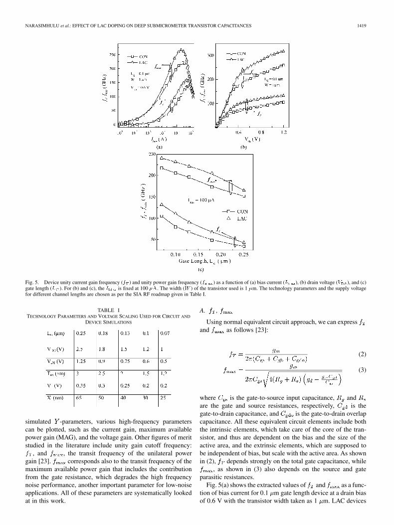
Fig. 3. Gate-to-source (C ) capacitance and gate-to-drain (C ) capacitancesas a function of drain voltage for different peak channel doping (doping atsource) concentrations for CON and LAC devices. The I is fixed at 100�A.
side. Hence, assuming this resistance to be large enough, theequivalent capacitance can be represented as
(1)
which makes the total gate-to-source capacitance lower in LACMOSFETs with aggressively scaled oxide thicknesses. Nearly a10% reduction in can be observed at all the drain voltageswith LAC devices.
Fig. 2(b) shows the gate-to-drain capacitance as a function ofdrain voltage at the same biasing current for the devices with anoxide thickness of 1.5 and 3 nm. In the same plot is also shown(right axis) the total gate capacitance ( )as a function of drain voltage for the device with an oxide thick-ness of 1.5 nm. The increased gate-to-drain capacitance in LACdevices is due to the increased inversion charge concentrationat the drain side because of the lower local in this region.The increased inversion charge increases the in this regionmaking to be higher, which can be seen from the (1). How-ever due to the channel pinchoff, the gate-to-drain capacitancetends to be similar for both the devices in the saturation region,as discussed earlier. Nearly a 10% lower gate parasitic capaci-tance is observed with lateral asymmetric channel profiles in thesaturation region of operation, as shown in Fig. 2(b), which isprimarily due to the reduction in the component. This in-creases the current gains in the RF operating range. The effectof this capacitance on the RF performance of MOSFETs is dis-cussed in the subsequent sections. We have also observed thatLAC doping results in higher values of for these devicescompared to CON devices. This is due to the higher body effectobserved in these devices, as reported earlier [22].
Fig. 3 shows the gate-to-source capacitance and gate-to-draincapacitance as a function of drain voltage for LAC deviceswith various peak channel doping concentrations (doping atthe source). This shows that as the peak channel doping isincreased the capacitance [in Fig. 2(b) inset] reduces dueto the reduced inversion charge at the source, which reducesthe net gate-to-source capacitance, as can be seen from the (1).One can notice that the device designed with a narrow and a
Fig. 4. Source-to- body (C ) and drain-to-body (C ) capacitances as afunction of drain voltage for CON and LAC devices at I = 100 �A andL = 0:1 �m.
higher pocket doping can give rise to an overall reduction of thedevice capacitances, in spite of a small increase in . For thesame biasing current, as the peak channel doping is increased,channel charge at the drain increases. This is because the deviceis becoming more strongly inverted near the drain side, whichmakes the and, hence, at the drain to be higher. Thisincreases the for LAC devices. However, one can notice alesser increase in values in the saturation region, for rea-sons explained earlier. Lower peak channel doping makes theLAC devices behave more like a conventional device, resultingin identical capacitances.
Fig. 4 shows the drain-to-body ( ) and source-to-body( ) capacitances for the two technologies (LAC and CON)as a function of drain voltage at a biasing current of 100 .From Fig. 4, it can be seen that the and capacitancesare considerably higher for LAC devices due to the higher bodyeffect in these MOSFETs as reported earlier, because of thelarger peak doping at the source [22]. As the inversion chargeprofile along the channel is uniform, as shown in the inset ofFig. 1(b), the body-effect factor dV dV is largerthan that of CON device. This makes (which is givenby ) of LAC device to increase causing a similarincrease in [23]. The higher body effect in these devicesmakes them suitable for dynamic threshold MOS (DTMOS)circuits.
IV. DEVICE RF PERFORMANCE ASPECTS
In the following sections, the effect of lateral asymmetricchannel doping on the device RF performance is exploredwith extensive device simulations and compared with CONdevices. For the simulations, all the technology parameters arekept identical for CON and LAC MOSFETs except for thechannel doping profiles. Poly-Si gate electrode with dopingequal to that of source/drain implantations is used for both thedevices. Silicidation process is used for source/drain to reducetheir contact resistance. In order to fully analyze the RF devicebehavior up to the GHz range, high-frequency -parametersimulations have been carried out over a frequency range1 to 100 GHz, using DESSIS device simulator. From these
NARASIMHULU et al.: EFFECT OF LAC DOPING ON DEEP SUBMICROMETER TRANSISTOR CAPACITANCES 1419
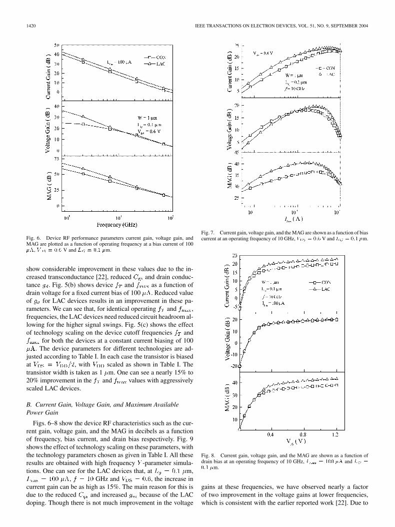
Fig. 5. Device unity current gain frequency (f ) and unity power gain frequency (f ) as a function of (a) bias current (I ), (b) drain voltage (V ), and (c)gate length (L ). For (b) and (c), the I is fixed at 100 �A. The width (W ) of the transistor used is 1 �m. The technology parameters and the supply voltagefor different channel lengths are chosen as per the SIA RF roadmap given in Table I.
TABLE ITECHNOLOGY PARAMETERS AND VOLTAGE SCALING USED FOR CIRCUIT AND
DEVICE SIMULATIONS
simulated -parameters, various high-frequency parameterscan be plotted, such as the current gain, maximum availablepower gain (MAG), and the voltage gain. Other figures of meritstudied in the literature include unity gain cutoff frequency:
, and , the transit frequency of the unilateral powergain [23]. corresponds also to the transit frequency of themaximum available power gain that includes the contributionfrom the gate resistance, which degrades the high frequencynoise performance, another important parameter for low-noiseapplications. All of these parameters are systematically lookedat in this work.
A. ,
Using normal equivalent circuit approach, we can expressand as follows [23]:
(2)
(3)
where is the gate-to-source input capacitance, andare the gate and source resistances, respectively, is thegate-to-drain capacitance, and is the gate-to-drain overlapcapacitance. All these equivalent circuit elements include boththe intrinsic elements, which take care of the core of the tran-sistor, and thus are dependent on the bias and the size of theactive area, and the extrinsic elements, which are supposed tobe independent of bias, but scale with the active area. As shownin (2), depends strongly on the total gate capacitance, while
, as shown in (3) also depends on the source and gateparasitic resistances.
Fig. 5(a) shows the extracted values of and as a func-tion of bias current for 0.1 m gate length device at a drain biasof 0.6 V with the transistor width taken as 1 m. LAC devices
1420 IEEE TRANSACTIONS ON ELECTRON DEVICES, VOL. 51, NO. 9, SEPTEMBER 2004
Fig. 6. Device RF performance parameters current gain, voltage gain, andMAG are plotted as a function of operating frequency at a bias current of 100�A, V = 0:6 V and L = 0:1 �m.
show considerable improvement in these values due to the in-creased transconductance [22], reduced and drain conduc-tance . Fig. 5(b) shows device and as a function ofdrain voltage for a fixed current bias of 100 . Reduced valueof for LAC devices results in an improvement in these pa-rameters. We can see that, for identical operating and ,frequencies, the LAC devices need reduced circuit headroom al-lowing for the higher signal swings. Fig. 5(c) shows the effectof technology scaling on the device cutoff frequencies and
for both the devices at a constant current biasing of 100. The device parameters for different technologies are ad-
justed according to Table I. In each case the transistor is biasedat , with scaled as shown in Table I. Thetransistor width is taken as 1 m. One can see a nearly 15% to20% improvement in the and values with aggressivelyscaled LAC devices.
B. Current Gain, Voltage Gain, and Maximum AvailablePower Gain
Figs. 6–8 show the device RF characteristics such as the cur-rent gain, voltage gain, and the MAG in decibels as a functionof frequency, bias current, and drain bias respectively. Fig. 9shows the effect of technology scaling on these parameters, withthe technology parameters chosen as given in Table I. All theseresults are obtained with high frequency -parameter simula-tions. One can see for the LAC devices that, at m,
, GHz and , the increase incurrent gain can be as high as 15%. The main reason for this isdue to the reduced and increased because of the LACdoping. Though there is not much improvement in the voltage
Fig. 7. Current gain, voltage gain, and the MAG are shown as a function of biascurrent at an operating frequency of 10 GHz, V = 0:6V and L = 0:1 �m.
Fig. 8. Current gain, voltage gain, and the MAG are shown as a function ofdrain bias at an operating frequency of 10 GHz, I = 100 �A and L =
0:1 �m.
gains at these frequencies, we have observed nearly a factorof two improvement in the voltage gains at lower frequencies,which is consistent with the earlier reported work [22]. Due to
NARASIMHULU et al.: EFFECT OF LAC DOPING ON DEEP SUBMICROMETER TRANSISTOR CAPACITANCES 1421
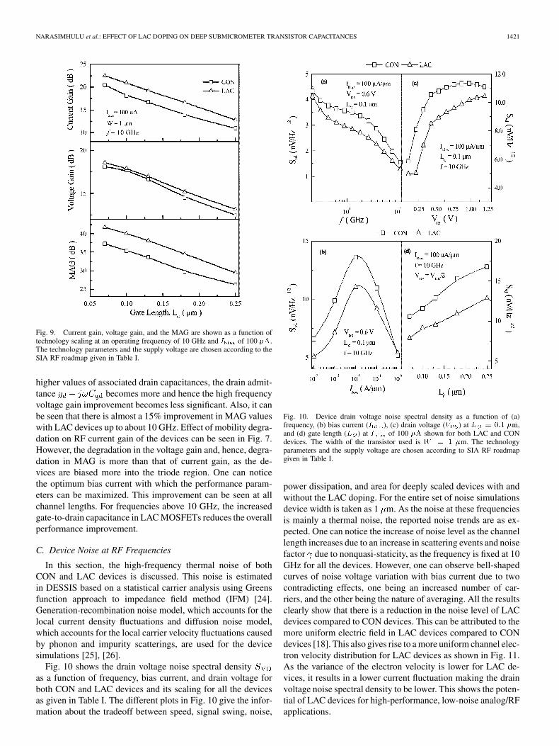
Fig. 9. Current gain, voltage gain, and the MAG are shown as a function oftechnology scaling at an operating frequency of 10 GHz and I of 100 �A.The technology parameters and the supply voltage are chosen according to theSIA RF roadmap given in Table I.
higher values of associated drain capacitances, the drain admit-tance becomes more and hence the high frequencyvoltage gain improvement becomes less significant. Also, it canbe seen that there is almost a 15% improvement in MAG valueswith LAC devices up to about 10 GHz. Effect of mobility degra-dation on RF current gain of the devices can be seen in Fig. 7.However, the degradation in the voltage gain and, hence, degra-dation in MAG is more than that of current gain, as the de-vices are biased more into the triode region. One can noticethe optimum bias current with which the performance param-eters can be maximized. This improvement can be seen at allchannel lengths. For frequencies above 10 GHz, the increasedgate-to-drain capacitance in LAC MOSFETs reduces the overallperformance improvement.
C. Device Noise at RF Frequencies
In this section, the high-frequency thermal noise of bothCON and LAC devices is discussed. This noise is estimatedin DESSIS based on a statistical carrier analysis using Greensfunction approach to impedance field method (IFM) [24].Generation-recombination noise model, which accounts for thelocal current density fluctuations and diffusion noise model,which accounts for the local carrier velocity fluctuations causedby phonon and impurity scatterings, are used for the devicesimulations [25], [26].
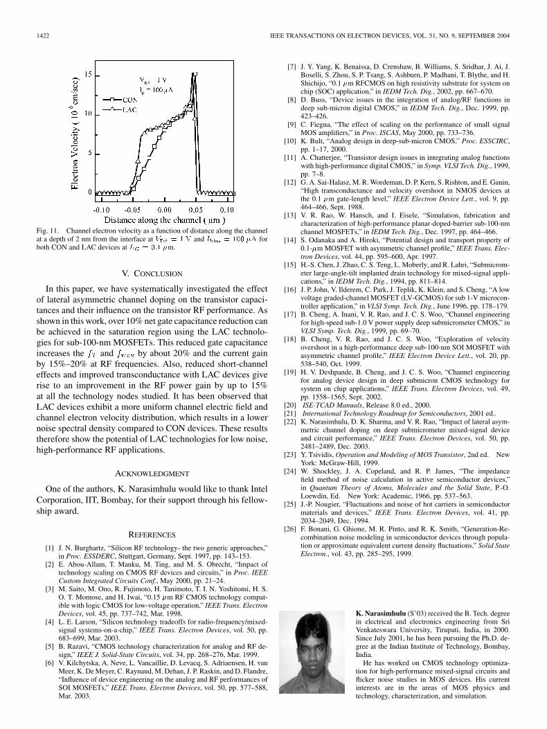
Fig. 10 shows the drain voltage noise spectral densityas a function of frequency, bias current, and drain voltage forboth CON and LAC devices and its scaling for all the devicesas given in Table I. The different plots in Fig. 10 give the infor-mation about the tradeoff between speed, signal swing, noise,
Fig. 10. Device drain voltage noise spectral density as a function of (a)frequency, (b) bias current (I ), (c) drain voltage (V ) at L = 0:1 �m,and (d) gate length (L ) at I of 100 �A shown for both LAC and CONdevices. The width of the transistor used is W = 1 �m. The technologyparameters and the supply voltage are chosen according to SIA RF roadmapgiven in Table I.
power dissipation, and area for deeply scaled devices with andwithout the LAC doping. For the entire set of noise simulationsdevice width is taken as 1 m. As the noise at these frequenciesis mainly a thermal noise, the reported noise trends are as ex-pected. One can notice the increase of noise level as the channellength increases due to an increase in scattering events and noisefactor due to nonquasi-staticity, as the frequency is fixed at 10GHz for all the devices. However, one can observe bell-shapedcurves of noise voltage variation with bias current due to twocontradicting effects, one being an increased number of car-riers, and the other being the nature of averaging. All the resultsclearly show that there is a reduction in the noise level of LACdevices compared to CON devices. This can be attributed to themore uniform electric field in LAC devices compared to CONdevices [18]. This also gives rise to a more uniform channel elec-tron velocity distribution for LAC devices as shown in Fig. 11.As the variance of the electron velocity is lower for LAC de-vices, it results in a lower current fluctuation making the drainvoltage noise spectral density to be lower. This shows the poten-tial of LAC devices for high-performance, low-noise analog/RFapplications.
1422 IEEE TRANSACTIONS ON ELECTRON DEVICES, VOL. 51, NO. 9, SEPTEMBER 2004
Fig. 11. Channel electron velocity as a function of distance along the channelat a depth of 2 nm from the interface at V = 1 V and I = 100 �A forboth CON and LAC devices at L = 0:1 �m.
V. CONCLUSION
In this paper, we have systematically investigated the effectof lateral asymmetric channel doping on the transistor capaci-tances and their influence on the transistor RF performance. Asshown in this work, over 10% net gate capacitance reduction canbe achieved in the saturation region using the LAC technolo-gies for sub-100-nm MOSFETs. This reduced gate capacitanceincreases the and by about 20% and the current gainby 15%–20% at RF frequencies. Also, reduced short-channeleffects and improved transconductance with LAC devices giverise to an improvement in the RF power gain by up to 15%at all the technology nodes studied. It has been observed thatLAC devices exhibit a more uniform channel electric field andchannel electron velocity distribution, which results in a lowernoise spectral density compared to CON devices. These resultstherefore show the potential of LAC technologies for low noise,high-performance RF applications.
ACKNOWLEDGMENT
One of the authors, K. Narasimhulu would like to thank IntelCorporation, IIT, Bombay, for their support through his fellow-ship award.
REFERENCES
[1] J. N. Burghartz, “Silicon RF technology- the two generic approaches,”in Proc. ESSDERC, Stuttgart, Germany, Sept. 1997, pp. 143–153.
[2] E. Abou-Allam, T. Manku, M. Ting, and M. S. Obrecht, “Impact oftechnology scaling on CMOS RF devices and circuits,” in Proc. IEEECustom Integrated Circuits Conf., May 2000, pp. 21–24.
[3] M. Saito, M. Ono, R. Fujimoto, H. Tanimoto, T. I. N. Yoshitomi, H. S.O. T. Momose, and H. Iwai, “0.15 �m RF CMOS technology compat-ible with logic CMOS for low-voltage operation,” IEEE Trans. ElectronDevices, vol. 45, pp. 737–742, Mar. 1998.
[4] L. E. Larson, “Silicon technology tradeoffs for radio-frequency/mixed-signal systems-on-a-chip,” IEEE Trans. Electron Devices, vol. 50, pp.683–699, Mar. 2003.
[5] B. Razavi, “CMOS technology characterization for analog and RF de-sign,” IEEE J. Solid-State Circuits, vol. 34, pp. 268–276, Mar. 1999.
[6] V. Kilchytska, A. Neve, L. Vancaillie, D. Levacq, S. Adriaensen, H. vanMeer, K. De Meyer, C. Raynaud, M. Dehan, J. P. Raskin, and D. Flandre,“Influence of device engineering on the analog and RF performances ofSOI MOSFETs,” IEEE Trans. Electron Devices, vol. 50, pp. 577–588,Mar. 2003.
[7] J. Y. Yang, K. Benaissa, D. Crenshaw, B. Williams, S. Sridhar, J. Ai, J.Boselli, S. Zhou, S. P. Tsang, S. Ashburn, P. Madhani, T. Blythe, and H.Shichijo, “0.1 �m RFCMOS on high resistivity substrate for system onchip (SOC) application,” in IEDM Tech. Dig., 2002, pp. 667–670.
[8] D. Buss, “Device issues in the integration of analog/RF functions indeep sub-micron digital CMOS,” in IEDM Tech. Dig., Dec. 1999, pp.423–426.
[9] C. Fiegna, “The effect of scaling on the performance of small signalMOS amplifiers,” in Proc. ISCAS, May 2000, pp. 733–736.
[10] K. Bult, “Analog design in deep-sub-micron CMOS,” Proc. ESSCIRC,pp. 1–17, 2000.
[11] A. Chatterjee, “Transistor design issues in integrating analog functionswith high-performance digital CMOS,” in Symp. VLSI Tech. Dig., 1999,pp. 7–8.
[12] G. A. Sai-Halasz, M. R. Wordeman, D. P. Kern, S. Rishton, and E. Ganin,“High transconductance and velocity overshoot in NMOS devices atthe 0.1 �m gate-length level,” IEEE Electron Device Lett., vol. 9, pp.464–466, Sept. 1988.
[13] V. R. Rao, W. Hansch, and I. Eisele, “Simulation, fabrication andcharacterization of high-performance planar-doped-barrier sub-100-nmchannel MOSFETs,” in IEDM Tech. Dig., Dec. 1997, pp. 464–466.
[14] S. Odanaka and A. Hiroki, “Potential design and transport property of0.1-�m MOSFET with asymmetric channel profile,” IEEE Trans. Elec-tron Devices, vol. 44, pp. 595–600, Apr. 1997.
[15] H.-S. Chen, J. Zhao, C. S. Teng, L. Moberly, and R. Lahri, “Submicrom-eter large-angle-tilt implanted drain technology for mixed-signal appli-cations,” in IEDM Tech. Dig., 1994, pp. 811–814.
[16] J. P. John, V. Ilderem, C. Park, J. Teplik, K. Klein, and S. Cheng, “A lowvoltage graded-channel MOSFET (LV-GCMOS) for sub 1-V microcon-troller application,” in VLSI Symp. Tech. Dig., June 1996, pp. 178–179.
[17] B. Cheng, A. Inani, V. R. Rao, and J. C. S. Woo, “Channel engineeringfor high-speed sub-1.0 V power supply deep submicrometer CMOS,” inVLSI Symp. Tech. Dig., 1999, pp. 69–70.
[18] B. Cheng, V. R. Rao, and J. C. S. Woo, “Exploration of velocityovershoot in a high-performance deep sub-100-nm SOI MOSFET withasymmetric channel profile,” IEEE Electron Device Lett., vol. 20, pp.538–540, Oct. 1999.
[19] H. V. Deshpande, B. Cheng, and J. C. S. Woo, “Channel engineeringfor analog device design in deep submicron CMOS technology forsystem on chip applications,” IEEE Trans. Electron Devices, vol. 49,pp. 1558–1565, Sept. 2002.
[20] ISE-TCAD Manuals, Release 8.0 ed., 2000.[21] International Technology Roadmap for Semiconductors, 2001 ed..[22] K. Narasimhulu, D. K. Sharma, and V. R. Rao, “Impact of lateral asym-
metric channel doping on deep submicrometer mixed-signal deviceand circuit performance,” IEEE Trans. Electron Devices, vol. 50, pp.2481–2489, Dec. 2003.
[23] Y. Tsividis, Operation and Modeling of MOS Transistor, 2nd ed. NewYork: McGraw-Hill, 1999.
[24] W. Shockley, J. A. Copeland, and R. P. James, “The impedancefield method of noise calculation in active semiconductor devices,”in Quantum Theory of Atoms, Molecules and the Solid State, P.-O.Loewdin, Ed. New York: Academic, 1966, pp. 537–563.
[25] J.-P. Nougier, “Fluctuations and noise of hot carriers in semiconductormaterials and devices,” IEEE Trans. Electron Devices, vol. 41, pp.2034–2049, Dec. 1994.
[26] F. Bonani, G. Ghione, M. R. Pinto, and R. K. Smith, “Generation-Re-combination noise modeling in semiconductor devices through popula-tion or approximate equivalent current density fluctuations,” Solid StateElectron., vol. 43, pp. 285–295, 1999.
K. Narasimhulu (S’03) received the B. Tech. degreein electrical and electronics engineering from SriVenkateswara University, Tirupati, India, in 2000.Since July 2001, he has been pursuing the Ph.D. de-gree at the Indian Institute of Technology, Bombay,India.
He has worked on CMOS technology optimiza-tion for high-performance mixed-signal circuits andflicker noise studies in MOS devices. His currentinterests are in the areas of MOS physics andtechnology, characterization, and simulation.
NARASIMHULU et al.: EFFECT OF LAC DOPING ON DEEP SUBMICROMETER TRANSISTOR CAPACITANCES 1423
Madhav P. Desai (M’01) received the B.Tech. de-gree in electrical engineering from the Indian Insti-tute of Technology (IIT), Bombay, India, in 1984, andthe M.S. and Ph.D. degrees from the University ofIllinois at Urbana-Champaign, Urbana, IL. His doc-toral work involved the study of the simulated an-nealing algorithm, which is a popular combinatorialoptimization technique.
From 1992 to 1996, he worked in the Semicon-ductor Engineering Group, Digital Equipment Cor-poration, Hudson, MA, where he was a Principal En-
gineer. While at Digital, he worked on timing verification, delay modeling, cir-cuit, and interconnect optimization and contributed to the design of two of theworld’s fastest CMOS microprocessors. He is currently an Associate Professor,Department of Electrical Engineering, IIT. He has served as a reviewer for theSIAM Journal on Control and various conferences. His interests are in the areasof VLSI design and design tools, circuits and systems, and combinatorial algo-rithms.
Dr. Desai has been the recipient of GTE and Schlumberger Graduate Fel-lowships. He was a reviewer for the IEEE TRANSACTIONS ON CIRCUITS AND
SYSTEMS and the IEEE TRANSACTIONS ON COMPUTERS.
Siva G. Narendra received the B.E. degree from theGovernment College of Technology, Coimbatore,India, in 1992, the M.S. degree from SycacuseUniversity, Syracuse, NY, in 1994, and the Ph.D.degree from Massachusetts Institute of Technology,Cambridge, in 2002.
He has been with Intel Laboratories, Hillsbor-ough, OR, since 1997, where his research areasinclude low-voltage MOS analog and digital circuitsand impact of MOS parameter variation on circuitdesign. He is Adjunct Faculty with the Department
of Electrical and Computer Engineering, Oregon State University, Corvallis,and has authored or co-authored over 44 papers and has 41 issued and 15pending patents. He is an Associate Editor for the IEEE TRANSACTIONS ON
VLSI SYSTEMS
Dr. Narendra is a member of the ISSCC, ISLPED, ISQED, and DAC/ISSCCstudent design contest technical program committees.
V. Ramgopal Rao (M’98–SM’02) received theM.Tech. degree from the Indian Institute of Tech-nology (IIT), Bombay, India, in 1991 and Dr.-Ing.(magna cum laude) degree from the Faculty of Elec-trical Engineering, Universitäet der Bundeswehr,Munich, Germany, in 1997. His doctoral thesis wason planar-doped-barrier sub-100-nm channel-lengthMOSFETs.
He was a Deutscher Akademischer Austauschdi-enst (DAAD) Fellow from 1994 to 1996, and againfrom February 1997 to July 1998, and in 2001, he
was a Visiting Scholar with the Electrical Engineering Department, Universityof California, Los Angeles. He is currently an Associate Professor in the De-partment of Electrical Engineering, IIT Bombay. His areas of interest includephysics, technology, and characterization of silicon CMOS devices, novel de-vice architectures, CMOS scaling for mixed signal applications, Flash mem-ories, bio-MEMS, and molecular electronics. He has over 130 publications inthese areas in refereed international journals and conference proceedings andholds two patents. He is an organizing committee member for the various inter-national conferences held in India.
Dr. Rao is a Fellow of IETE. He is an Associate Editor for the IEEETRANSACTIONS ON ELECTRON DEVICES in the CMOS Devices and Technologyarea. He is Chairman of the IEEE AP/ED Bombay Chapter and was organizingcommittee chair for the 17th International Conference on VLSI Design. He isalso a Member of the Government of India’s group on Nanotechnology.