Embed Size (px)
Citation preview

The Effect of Mechanical Loading on theFrequency of an Oscillator Circuit
Report Contributors: Jonathan A. Ward1,2,
Vladimir Lapin1 and William Lee1
Study Group Contributors: Chris Budd3, Mark Cooker4,
Paul J. Dellar 5, Martin Hayes6, Poul Hjorth7,
Olga Korostynska8 and Arno Mayrhofer1
Industry Representative: Sandra Healy9
1MACSI, Department of Mathematics and Statistics, University of Limerick, Ireland2Report coordinator, [email protected] of Mathematical Sciences, University of Bath, United Kingdom4School of Mathematics, University of East Anglia, United Kingdom5OCIAM, Mathematical Institute, University of Oxford, United Kingdom6Department of Electronic and Computer Engineering, University of Limerick, Ireland7Department of Mathematics, Technical University of Denmark, Denmark8Microelectronic and Semiconductor Research Centre, University of Limerick, Ireland9Analog Devices, Raheen Industrial Estate, Raheen, Limerick, Ireland
Abstract
We investigate the effect of mechanical strain on the frequency of an electronic oscillator em-bedded in an integrated circuit. This analysis is aimed at explaining a 1% inaccuracy in theoscillator frequency under test conditions prescribed by a leading supplier of semi-conductordevices. During the test the package containing the oscillator was clamped to a circuit boardby mechanical pressure. By considering the nature of the oscillator we show that tensile strainsof the order of 10−4 could explain the observations via the piezoresistance effect. Both a simpleone-dimensional analysis based on the beam equation and an elastic finite element simulationshow that strains of this magnitude can be generated during the test.
30
1 Introduction
Silicon chips, or Integrated Circuits (ICs), perform the underlying functions of most modernelectronic devices. These miniature circuit boards consist of millions of electronic devices suchas transistors, capacitors, resistors and diodes. During manufacturing, the components in ICsare built up and connected together in layers on the surface of a silicon substrate, known as adie, via etching, deposition and photo-lithography [1]. The die are then moulded into a plasticcase, which we refer to as a package.
Chips are typically tested before being sold and may be moved mechanically between a varietyof test sites. During testing, a downward force of the order of 100 N is exerted on the chip toensure good electrical contact. A particular chip manufactured by a leading semi-conductorsupplier (who we refer to simply as “the supplier”), contains an oscillator circuit whose frequencymust reach a ±1% accuracy specification over a temperature range of −40 to +105C and 100%of the chips are tested. However, the supplier observed that the loads experienced by the chipcould lead to significant errors in the accuracy of the oscillator circuit, possibly due to somesort of piezo effect.
In this paper we investigate how a vertical load placed on such a chip might result in errors inthe oscillator frequency. This problem was presented at the 70th European Study Group withIndustry (ESGI), hosted by MACSI at the University of Limerick in 2009, funded by the ScienceFoundation Ireland mathematics initiative grant. In Section 2 we give a detailed descriptionof the problem including the structure of the package, the test-rig set-up, data concerning thefrequency response to loading and how the chips are “trimmed” to the required frequency. Wedescribe in Section 3 how the key components in the oscillator circuit, namely capacitors andresistors, might affect the oscillator frequency when subjected to a vertical load. In Section 4we discuss mechanical modelling of the elastic response of the package to loading using thebeam equation and finite element elasticity calculations. Finally we summarise our results inSection 5.
2 Detailed Problem Description and Data
2.1 Package Design
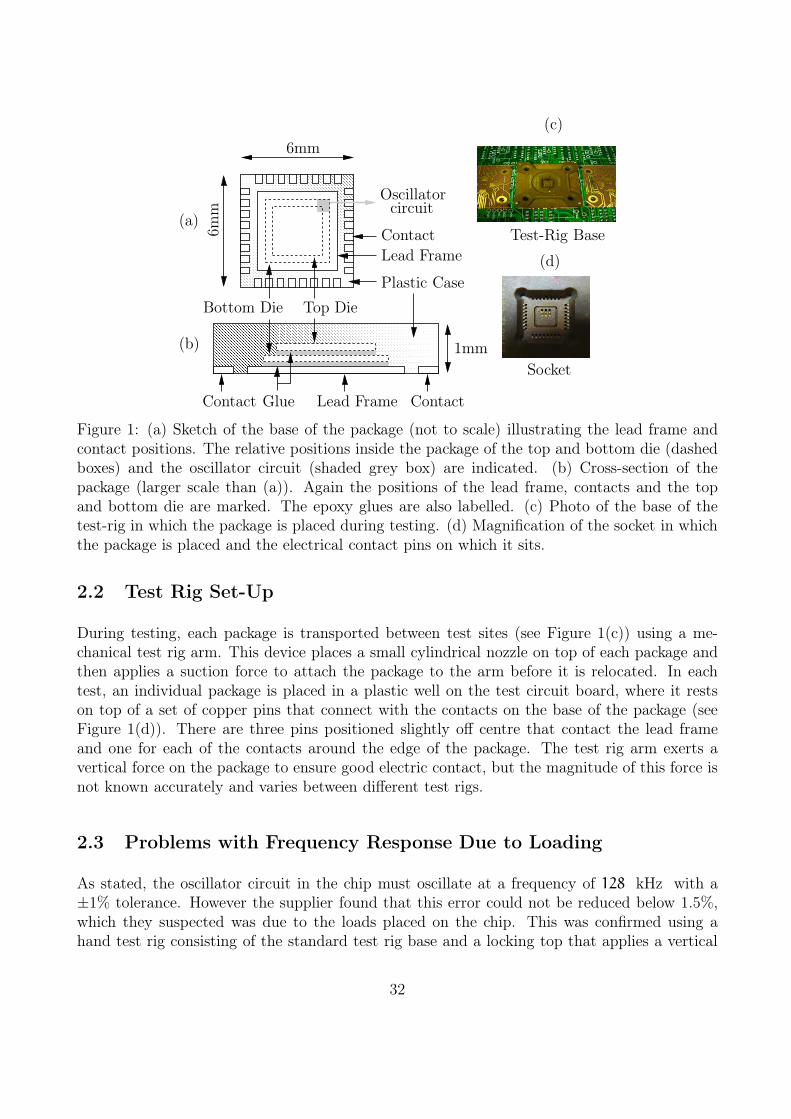
Due to commercial sensitivity, details of the specific package and chip design cannot be pre-sented in this paper. A sketch of the package is illustrated in Figure 1(a). There are two diein each package, one of which is smaller and sits on top of the larger (see Figure 1(b)). Theseare placed on a copper base known as the lead frame. The three layers are aligned at theircentres and attached using epoxy adhesives. There are 8 contacts along each side of the baseof the package that are connected to the die via small wires. The die, lead frame, contacts andconnections are moulded into a plastic case.
31
(a)
(c)
(d)
(b)
Lead Frame
Lead Frame
Bottom Die Top Die
Contact Contact
Contact
Oscillatorcircuit
6mm
6mm
1mm
Test-Rig Base
Socket
Glue
Plastic Case
Figure 1: (a) Sketch of the base of the package (not to scale) illustrating the lead frame andcontact positions. The relative positions inside the package of the top and bottom die (dashedboxes) and the oscillator circuit (shaded grey box) are indicated. (b) Cross-section of thepackage (larger scale than (a)). Again the positions of the lead frame, contacts and the topand bottom die are marked. The epoxy glues are also labelled. (c) Photo of the base of thetest-rig in which the package is placed during testing. (d) Magnification of the socket in whichthe package is placed and the electrical contact pins on which it sits.
2.2 Test Rig Set-Up
During testing, each package is transported between test sites (see Figure 1(c)) using a me-chanical test rig arm. This device places a small cylindrical nozzle on top of each package andthen applies a suction force to attach the package to the arm before it is relocated. In eachtest, an individual package is placed in a plastic well on the test circuit board, where it restson top of a set of copper pins that connect with the contacts on the base of the package (seeFigure 1(d)). There are three pins positioned slightly off centre that contact the lead frameand one for each of the contacts around the edge of the package. The test rig arm exerts avertical force on the package to ensure good electric contact, but the magnitude of this force isnot known accurately and varies between different test rigs.
2.3 Problems with Frequency Response Due to Loading
As stated, the oscillator circuit in the chip must oscillate at a frequency of 128 kHz with a±1% tolerance. However the supplier found that this error could not be reduced below 1.5%,which they suspected was due to the loads placed on the chip. This was confirmed using ahand test rig consisting of the standard test rig base and a locking top that applies a vertical
32
% Frequency Change vs. Applied Mass
%Fre
quen
cyC
han
ge
Force (kg equivalent)
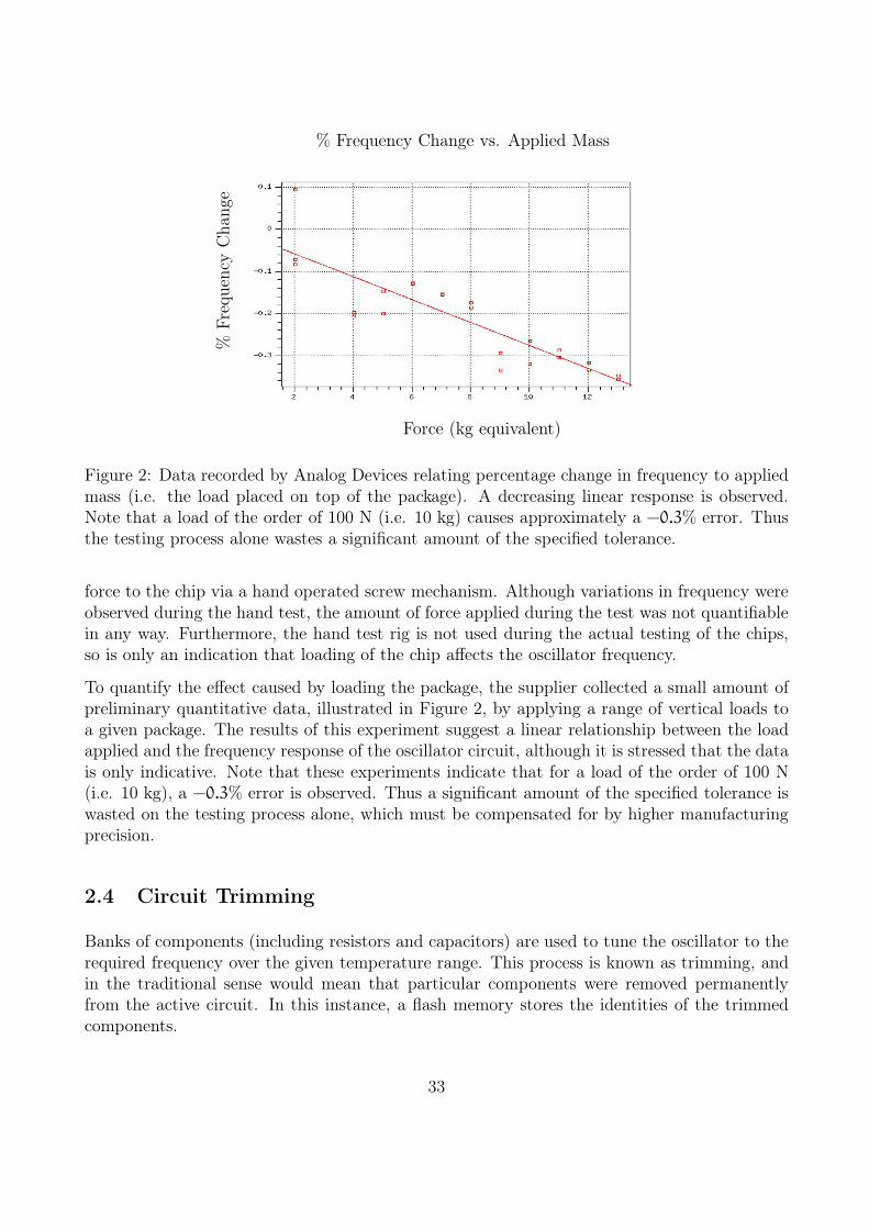
Figure 2: Data recorded by Analog Devices relating percentage change in frequency to appliedmass (i.e. the load placed on top of the package). A decreasing linear response is observed.Note that a load of the order of 100 N (i.e. 10 kg) causes approximately a −0.3% error. Thusthe testing process alone wastes a significant amount of the specified tolerance.
force to the chip via a hand operated screw mechanism. Although variations in frequency wereobserved during the hand test, the amount of force applied during the test was not quantifiablein any way. Furthermore, the hand test rig is not used during the actual testing of the chips,so is only an indication that loading of the chip affects the oscillator frequency.
To quantify the effect caused by loading the package, the supplier collected a small amount ofpreliminary quantitative data, illustrated in Figure 2, by applying a range of vertical loads toa given package. The results of this experiment suggest a linear relationship between the loadapplied and the frequency response of the oscillator circuit, although it is stressed that the datais only indicative. Note that these experiments indicate that for a load of the order of 100 N(i.e. 10 kg), a −0.3% error is observed. Thus a significant amount of the specified tolerance iswasted on the testing process alone, which must be compensated for by higher manufacturingprecision.
2.4 Circuit Trimming
Banks of components (including resistors and capacitors) are used to tune the oscillator to therequired frequency over the given temperature range. This process is known as trimming, andin the traditional sense would mean that particular components were removed permanentlyfrom the active circuit. In this instance, a flash memory stores the identities of the trimmedcomponents.
33
3 Piezo Effects in the Oscillator Circuit
We now describe how the response of the key components in the oscillator circuit might beaffected by mechanical loading. An oscillator circuit provides a continuous, synchronised triggersignal to the rest of the devices on the chip from which information is processed [2]. Due tocommercial sensitivity (and its shear complexity), the specific design of the oscillator circuitin question was not provided. However, there are two main types of electronic oscillators, RCcircuits (composed of Resistors and C apacitors) and LC circuits (composed of inductors andcapacitors). Inductors are not common in ICs, hence we focus on the first type of oscillator.
The oscillation frequency of an RC circuit is f = 1/(2πRC) [1], where R and C are the effectiveresistance and capacitance of the banks of resistors and capacitors on the chip respectively.Typical values of resistance and capacitance are R = 10kΩ and C = 100pF. A small fractionalincrease, δ, in the product of the resistance and capacitance results in a fractional decrease infrequency, f, of the same amount,
f =1
2πRC(1+ δ)≈ 1
2πRC(1− δ). (3.1)
Thus a 1% drop in frequency requires a 1% increase in capacitance or resistance (i.e. δ = 0.01).We now consider whether the kind of mechanical load experienced by the chip can give rise tosuch changes in the capacitance or resistance.
3.1 Capacitor Response
Capacitors consist of two parallel conducting plates with a dielectric material sandwiched be-tween. The plane of the conducting plates is perpendicular to the applied load in this case.The value of capacitance is given by
C =εAC
d, (3.2)
where ε is the permittivity of the dielectric, AC is the area of the plates and d is the distancebetween them. Thus the capacitance increases in response to a decrease in distance betweenplates, which might be expected when subjected to a vertical load as in this scenario.
However, the dielectric material is typically silicon dioxide, which is a very stiff material. Givena 100N force placed on a package approximately 6mm×6mm, the resulting pressure P is 4 MPa.The Young’s modulus E of silicon dioxide is approximately 100 GPa, thus considering Hooke’slaw, the resulting strain (and hence the change in distance between plates) is
P
E≃ 3× 10⁻⁵, (3.3)
which is much smaller then the 1.5% change required.
34
Thus the change in capacitance due to the plates being forced closer together cannot be re-sponsible for the observed 1.5% change in frequency. The deformation of the dielectric doesnot change its permittivity either, since silicon dioxide does exhibit any piezoelectric effects [3].
3.2 Resistor Response
Piezoresistance is a well known effect that occurs when resistors are subject to mechanicaldeformation [4]. The resistance of a conducting element with a fixed cross section of area AR
and length l is given by
R0 = ρ0
l
AR
, (3.4)
where ρ0 is resistivity. If the shape of the resistor is changed, the subsequent change in resistanceis related to the strain ǫ = ∆l/l via
∆R
R0
= Gǫ, (3.5)
where G is known as the gauge factor,
G := (1+ 2ν) +(∆ρ/ρ0)
ǫ, (3.6)
and ν is the Poisson’s ratio of the resistor material, which accounts for the change in cross-sectional area due to the change in length. It is known that the resistivity change (∆ρ/ρ0)/ǫ forsemiconductors is much larger than the dimensional change (1+ 2ν) [5]. In fact gauge factorsas large as 100 have been measured for p-type silicon and as low as −100 in n-type silicon [4, 6].Thus to observe a 1% decrease in frequency due to piezoresistance, we would need strains ofthe order of 10−4.
4 Mechanical Modelling
To calculate the strains induced by mechanical loading, we first consider a simple method inwhich the package is modelled using a one-dimensional beam equation. This approach neglectsinhomogeneities in the package and corner effects that arise in the plane perpendicular to theloading due to the stacking of the die. Thus we develop a more sophisticated two-dimensionalaxisymmetric model of the composite package that we solve using finite element software inCOMSOL, from which we obtain the strain field in a cross-section of the package.
4.1 One-Dimensional Model
A simple approach to calculating approximate values of the strain in the package is to modelthe entire assembly using the one-dimensional beam equation [7]. Thus we consider the package
35
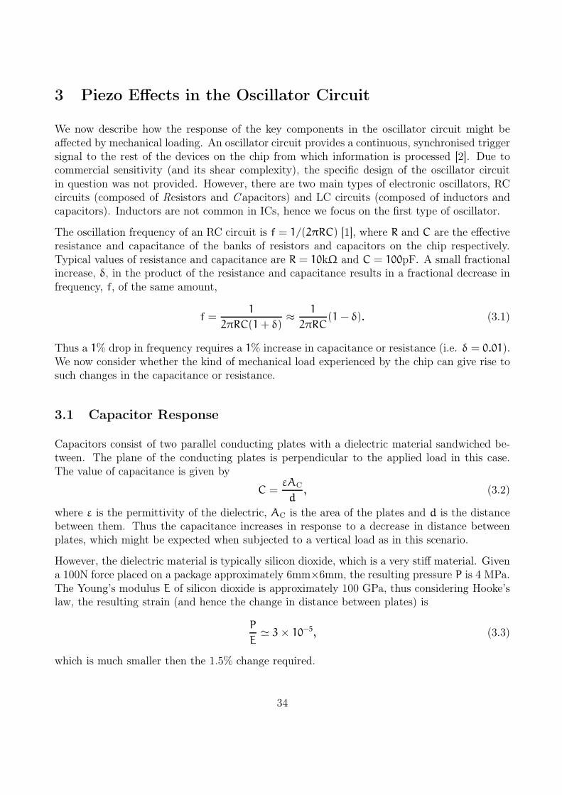
Figure 3: Geometry in which the package is modelled as an elastic beam. The pins are modelledas Hookean springs, while the die is modelled as two localised forces.
to be elastically homogeneous and made entirely of silicon. The geometry used in this case isshown in Figure 3. The width of the package is 2A and the load is represented by two localisedforces F imposed at x = ±B. The pins are modelled as Hookean springs, positioned at the edgesof the package (x = ±A) and the centre (x = 0) with spring constants k1 and k2 respectively.The spring constant of the outer pins is chosen to be five times larger than at the centre toreflect that there are more pins around the edge of the package. However, the spring constantsare not known accurately,thus we consider two cases: (a), stiff springs, k1 = 500 MN/m andk2 = 100 MN/m ; and (b), flexible springs, k1 = 50 MN/m and k2 = 10 MN/m .
As noted, we model the vertical displacement u(x) of the package using the one-dimensionalbeam equation with point forcing,
EId4u
dx4= F [δ(x+ B) + δ(x − B)] − k2δ(x)u(x), (4.1)
where E is the Young’s modulus of the package and I is the second moment of area. Theboundary conditions at the edges of the package are
EId3u
dx3
∣∣∣∣x=±A
= −k1u(±A) and (4.2)
d2u
dx2
∣∣∣∣x=±A
= 0. (4.3)
Note that at each discontinuity, the zeroth, first and second derivatives must be equal. Theseequations form a linear system whose solution is a piecewise cubic polynomial in x. Thepolynomial coefficients in each of the four regions along the beam can be easily calculated usingcomputer algebra, however they are somewhat complicated and hence we do not reproduce themhere.
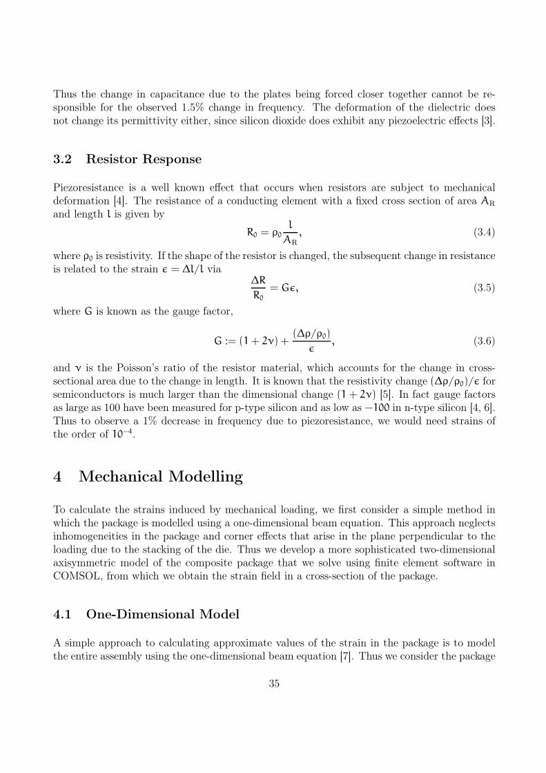
The parameters used in the calculation are given in Table 1. The displacement along the beamu(x) is illustrated in Figure 4(a) for the stiff springs case and in Figure 4(b) for the case flexiblesprings case. These illustrate that the stiffness of the pins can affect the overall shape of thepackage: stiffer pins result in a “W”–shape, whereas flexible pins give rise to a concave shape.
36
Parameter Value
A 3 mmB 2 mmh 1 mmE 150 GPaF 50 N
Table 1: Values of parameters used in the calculation. In addition, two different types of springconstant are considered: stiff springs, k1 = 500 MN/m and k2 = 100 MN/m ; and flexiblesprings, k1 = 50 MN/m and k2 = 10 MN/m .
Figure 4: Displacement calculated from equations 4.1–4.3 for the cases (a) (stiff springs) and(b) (flexible springs).
Given the displacement and the height of the package h, we can calculate the tensile strain,
ǫxx =h
2
d2u
dx2, (4.4)
at the base of the package. This is plotted in Figure 5(a) and (b) for the stiff and flexible pincases respectively. In both instances, the magnitude of the strains are large enough to accountfor the observed frequency variations due to piezoresistive effects. The stiffer springs used inFigure 4(a) result in a region of compression at the centre of the package. Note that in bothcases, the largest strains occur in regions of extension (positive strain) where the downwardload is applied. The strain is zero at the edges due to the boundary conditions (4.3).
4.2 Axisymmetric Finite Element Model
Although the simple approach using the beam equation shows some promising results, it isbased on a very restrictive set of assumptions, in particular that the package is homogeneousand can be represented as thin rod. A linear elasticity model of the composite package can be
37
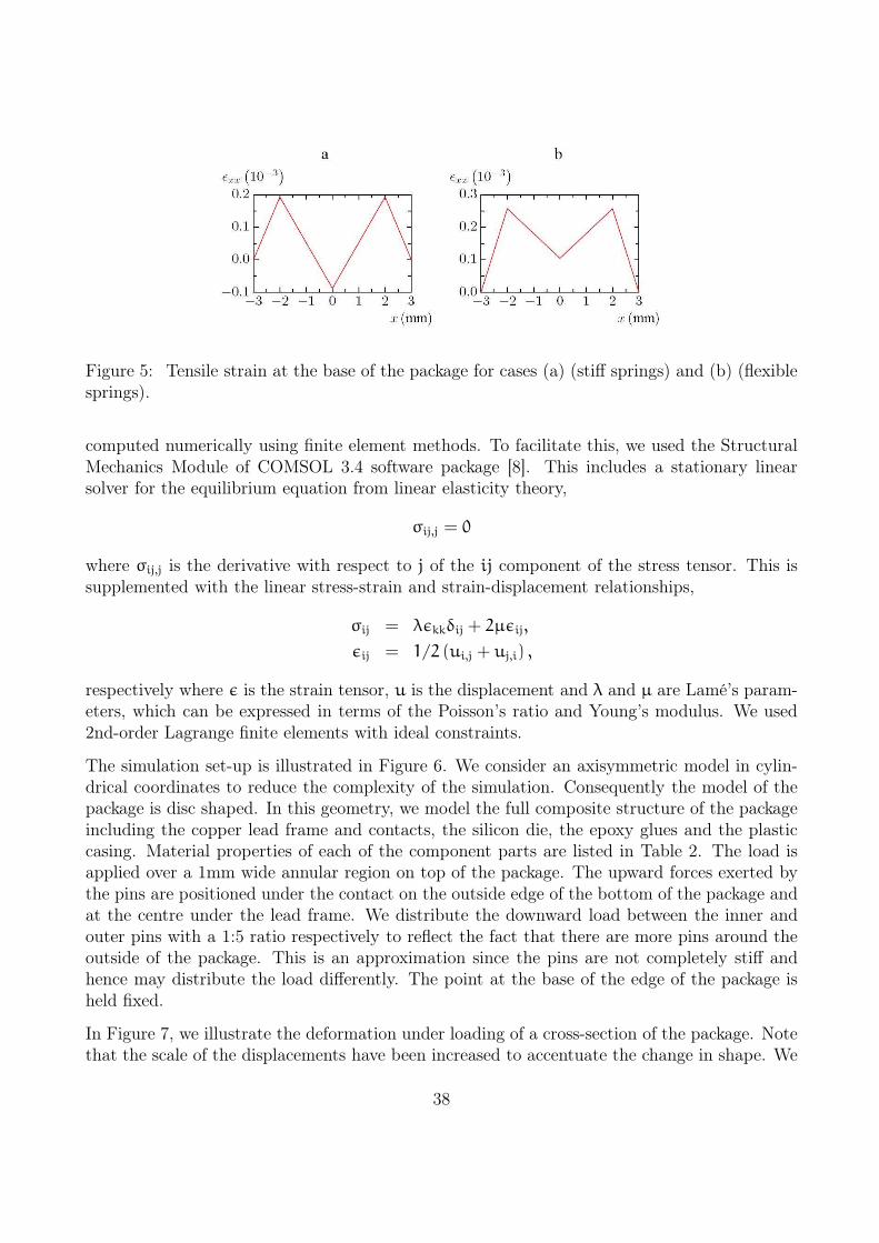
Figure 5: Tensile strain at the base of the package for cases (a) (stiff springs) and (b) (flexiblesprings).
computed numerically using finite element methods. To facilitate this, we used the StructuralMechanics Module of COMSOL 3.4 software package [8]. This includes a stationary linearsolver for the equilibrium equation from linear elasticity theory,
σij,j = 0
where σij,j is the derivative with respect to j of the ij component of the stress tensor. This issupplemented with the linear stress-strain and strain-displacement relationships,
σij = λǫkkδij + 2µǫij,
ǫij = 1/2 (ui,j + uj,i) ,
respectively where ǫ is the strain tensor, u is the displacement and λ and µ are Lamé’s param-eters, which can be expressed in terms of the Poisson’s ratio and Young’s modulus. We used2nd-order Lagrange finite elements with ideal constraints.
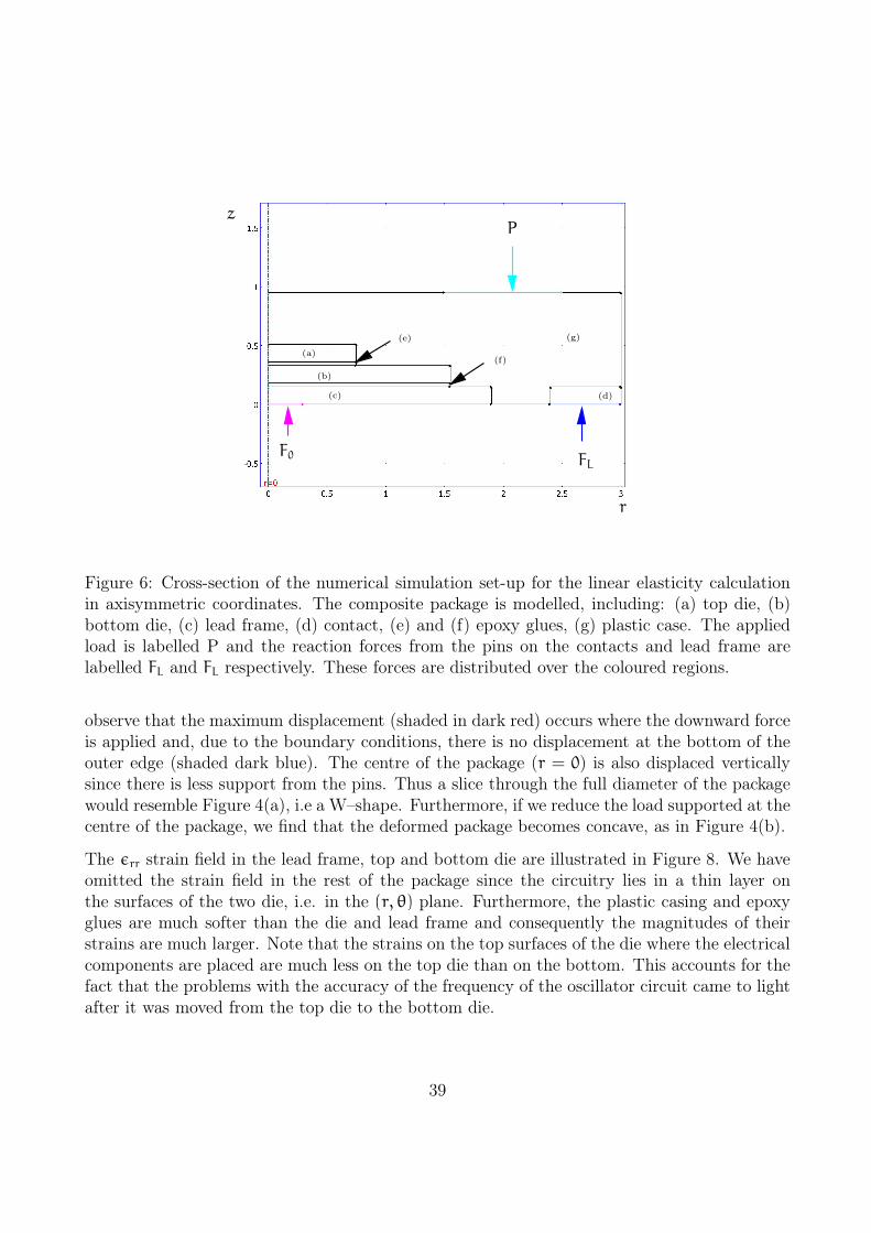
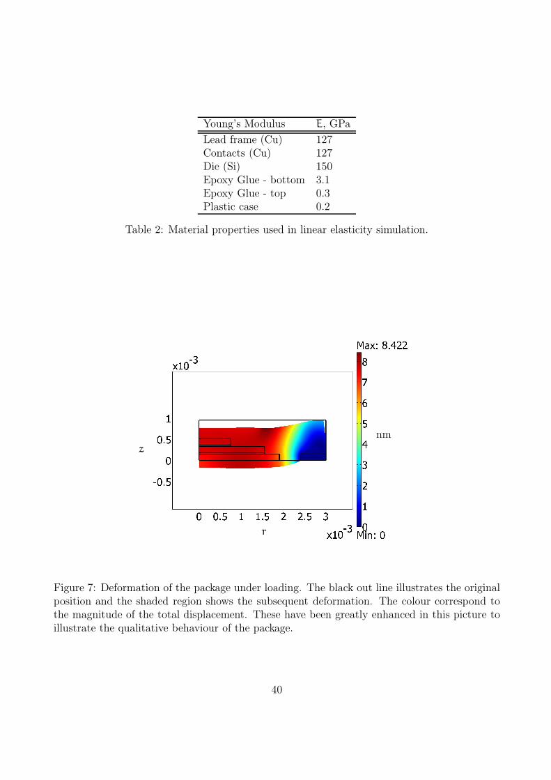
The simulation set-up is illustrated in Figure 6. We consider an axisymmetric model in cylin-drical coordinates to reduce the complexity of the simulation. Consequently the model of thepackage is disc shaped. In this geometry, we model the full composite structure of the packageincluding the copper lead frame and contacts, the silicon die, the epoxy glues and the plasticcasing. Material properties of each of the component parts are listed in Table 2. The load isapplied over a 1mm wide annular region on top of the package. The upward forces exerted bythe pins are positioned under the contact on the outside edge of the bottom of the package andat the centre under the lead frame. We distribute the downward load between the inner andouter pins with a 1:5 ratio respectively to reflect the fact that there are more pins around theoutside of the package. This is an approximation since the pins are not completely stiff andhence may distribute the load differently. The point at the base of the edge of the package isheld fixed.
In Figure 7, we illustrate the deformation under loading of a cross-section of the package. Notethat the scale of the displacements have been increased to accentuate the change in shape. We
38
z
r
P
F0 FL
(a)
(b)
(c) (d)
(e)
(f)
(g)
Figure 6: Cross-section of the numerical simulation set-up for the linear elasticity calculationin axisymmetric coordinates. The composite package is modelled, including: (a) top die, (b)bottom die, (c) lead frame, (d) contact, (e) and (f) epoxy glues, (g) plastic case. The appliedload is labelled P and the reaction forces from the pins on the contacts and lead frame arelabelled FL and FL respectively. These forces are distributed over the coloured regions.
observe that the maximum displacement (shaded in dark red) occurs where the downward forceis applied and, due to the boundary conditions, there is no displacement at the bottom of theouter edge (shaded dark blue). The centre of the package (r = 0) is also displaced verticallysince there is less support from the pins. Thus a slice through the full diameter of the packagewould resemble Figure 4(a), i.e a W–shape. Furthermore, if we reduce the load supported at thecentre of the package, we find that the deformed package becomes concave, as in Figure 4(b).
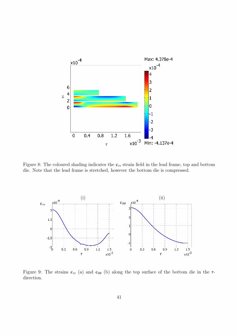
The ǫrr strain field in the lead frame, top and bottom die are illustrated in Figure 8. We haveomitted the strain field in the rest of the package since the circuitry lies in a thin layer onthe surfaces of the two die, i.e. in the (r, θ) plane. Furthermore, the plastic casing and epoxyglues are much softer than the die and lead frame and consequently the magnitudes of theirstrains are much larger. Note that the strains on the top surfaces of the die where the electricalcomponents are placed are much less on the top die than on the bottom. This accounts for thefact that the problems with the accuracy of the frequency of the oscillator circuit came to lightafter it was moved from the top die to the bottom die.
39
Young’s Modulus E, GPa
Lead frame (Cu) 127Contacts (Cu) 127Die (Si) 150Epoxy Glue - bottom 3.1Epoxy Glue - top 0.3Plastic case 0.2
Table 2: Material properties used in linear elasticity simulation.
r
z
nm
Figure 7: Deformation of the package under loading. The black out line illustrates the originalposition and the shaded region shows the subsequent deformation. The colour correspond tothe magnitude of the total displacement. These have been greatly enhanced in this picture toillustrate the qualitative behaviour of the package.
40
r
z
Figure 8: The coloured shading indicates the ǫrr strain field in the lead frame, top and bottomdie. Note that the lead frame is stretched, however the bottom die is compressed.
(i) (ii)ǫrr
ǫθθ
r r
Figure 9: The strains ǫrr (a) and ǫθθ (b) along the top surface of the bottom die in the r-direction.
41
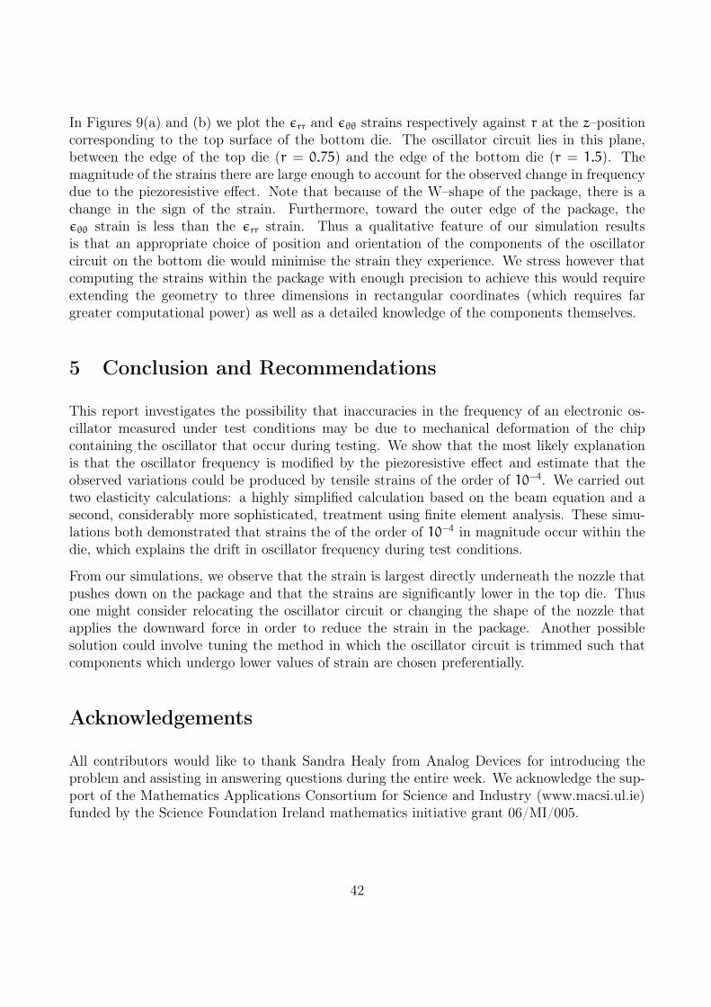
In Figures 9(a) and (b) we plot the ǫrr and ǫθθ strains respectively against r at the z–positioncorresponding to the top surface of the bottom die. The oscillator circuit lies in this plane,between the edge of the top die (r = 0.75) and the edge of the bottom die (r = 1.5). Themagnitude of the strains there are large enough to account for the observed change in frequencydue to the piezoresistive effect. Note that because of the W–shape of the package, there is achange in the sign of the strain. Furthermore, toward the outer edge of the package, theǫθθ strain is less than the ǫrr strain. Thus a qualitative feature of our simulation resultsis that an appropriate choice of position and orientation of the components of the oscillatorcircuit on the bottom die would minimise the strain they experience. We stress however thatcomputing the strains within the package with enough precision to achieve this would requireextending the geometry to three dimensions in rectangular coordinates (which requires fargreater computational power) as well as a detailed knowledge of the components themselves.
5 Conclusion and Recommendations
This report investigates the possibility that inaccuracies in the frequency of an electronic os-cillator measured under test conditions may be due to mechanical deformation of the chipcontaining the oscillator that occur during testing. We show that the most likely explanationis that the oscillator frequency is modified by the piezoresistive effect and estimate that theobserved variations could be produced by tensile strains of the order of 10−4. We carried outtwo elasticity calculations: a highly simplified calculation based on the beam equation and asecond, considerably more sophisticated, treatment using finite element analysis. These simu-lations both demonstrated that strains the of the order of 10−4 in magnitude occur within thedie, which explains the drift in oscillator frequency during test conditions.
From our simulations, we observe that the strain is largest directly underneath the nozzle thatpushes down on the package and that the strains are significantly lower in the top die. Thusone might consider relocating the oscillator circuit or changing the shape of the nozzle thatapplies the downward force in order to reduce the strain in the package. Another possiblesolution could involve tuning the method in which the oscillator circuit is trimmed such thatcomponents which undergo lower values of strain are chosen preferentially.
Acknowledgements
All contributors would like to thank Sandra Healy from Analog Devices for introducing theproblem and assisting in answering questions during the entire week. We acknowledge the sup-port of the Mathematics Applications Consortium for Science and Industry (www.macsi.ul.ie)funded by the Science Foundation Ireland mathematics initiative grant 06/MI/005.
42

Bibliography
[1] A.R. Hambley. Electronics. Prentice-Hall, second edition, 2000.
[2] Colin D. Simpson. Industrial Electronics. Prentice-Hall, first edition, 1996.
[3] L.D. Landau, E.M. Liftshitz, and L.P. Pitaevskii. Electrodynamics of Continuous Media.Butterworth-Heinemann, second edition, 1984.
[4] S. Middelhoek and S.A. Audet. Silicon Sensors. Academic Press Ltd., first edition, 1989.
[5] Yozo Kanda. Piezoresistance effect of silicon. Sensor Actuat. A, 28:83–91, 1991.
[6] Charles S. Smith. Piezoresistance effect in germanium and silicon. Phys. Rev., 94(1):42–49,1954.
[7] L.D. Landau and E.M. Liftshitz. Theory of Elasticity. Butterworth-Heinemann, thirdedition, 1986.
[8] COMSOL AB. COMSOL Multiphysics Modeling Guide. COMSOL Ltd, 3.4 edition, 2007.
43