Embed Size (px)
Citation preview

The Dynamic Interplay Between Spacecraft Charging, Space Environment Interactions
and Evolving Materials
Los Alamos New Mexico February 2, 2012
J.R. Dennison
Materials Physics Group Physics Department, Utah State University

Acknowledgements
Support & Collaborations NASA SEE Program
JWST (GSFC/MSFC) SPM (JHU/APL) RBSP (JHU/APL) Solar Sails (JPL) AFRL Boeing Ball Aerospace Orbital National Research Council
USU Materials Physics Group

4
Nothing endures but change. --Heraclitus of Ephesus (c. 495 BC)
Shit Happens…..

5
A simplified approach to spacecraft charging modeling…
Satellite Moving through Space
I+
γ
e-
Space Plasma Environment
Spacecraft Potential Models
Materials Properties
+ _
m

9/24/12 LANL Seminar 6
The Space Environment
Typical Space Electron Flux Spectra [Larsen].
Incident Fluxes of: • Electrons • Ions • Photons • Particles
Solar wind and Earth’s magneto-sphere structure.
Solar Electro-magnetic Spectrum.

7
#1 Non-static Spacecraft Materials Properties #2 Non-static Spacecraft Charging Models
These result from the complex dynamic interplay between space environment, satellite motion, and materials properties
Specific focus of this talk is the change in materials properties as a function of time , position, energy, and charge: Time (Aging), t Energy
• Temperature, kB T • Deposited Energy (Dose), D • Energy Deposition (Dose) Rate, Ď
Charge • Accumulated Charge, ΔQ or ΔV • Charge Profiles, Q(z) • Charge Rate (Current), Ŏ • Conductivity Profiles, σ(z)
Dale Ferguson’s “New Frontiers in Spacecraft Charging”

Charging codes such as NASCAP-2K or SPENVIS and NUMIT2 or DICTAT require:
Charge Accumulation • Electron yields • Ion yields • Photoyields • Luminescence
Charge Transport • Conductivity • RIC • Dielectric Constant • ESD • Range ABSOLUTE values as functions of materials species, flux, fluence, and energy.
What do you need to know about the materials properties?
I+
γ
e-
+ _
Complex dynamic interplay between space environment, satellite motion, and materials properties
Dynamics of the space environment and satellite motion lead to dynamic spacecraft charging • Solar Flares • Rotational eclipse
Table 2.1. Parameters for NASCAP Materials Properties
Parameter Value
[1] Relative dielectric constant; εr (Input as 1 for conductors) 1, NA
[2] Dielectric film thickness; d 0 m, NA
[3] Bulk conductivity; σo (Input as -1 for conductors) -1; (4.26 ± 0.04) · 107 ohm-1·m-1
[4] Effective mean atomic number <Zeff> 50.9 ± 0.5
[5] Maximum SE yield for electron impact; δmax 1.47 ± 0.01
[6] Primary electron energy for δmax; Emax (0.569 ± 0.07) keV
[7] First coefficient for bi-exponential range law, b1 1 Å, NA
[8] First power for bi-exponential range law, n1 1.39 ± 0.02
[9] Second coefficient for bi-exponential range law, b2 0 Å
[10] Second power for bi-exponential range law, n2 0
[11] SE yield due to proton impact δH(1keV) 0.3364 ± 0.0003
[12] Incident proton energy for δHmax; E
Hmax (1238 ± 30) keV
[13] Photoelectron yield, normally incident sunlight, jpho (3.64 ± 0.4) · 10-5 A·m-2
[14] Surface resistivity; ρs (Input as -1 for non-conductors) -1 ohms·square-1, NA
[15] Maximum potential before discharge to space; Vmax 10000 V, NA
[16] Maximum surface potential difference before dielectric breakdown discharge; Vpunch
2000 V, NA
[17] Coefficient of radiation-induced conductivity, σr; k 0 ohms-1·m-1, NA
[18] Power of radiation-induced conductivity, σr; Δ 0, NA

9
USU Experimental Capabilities Absolute Yields • SEE, BSE, emission spectra , (<20 eV to 30 keV) •Angle resolved electron emission spectra • Photoyield (~160 nm to 1200 nm) • Ion yield (He, Ne, Ar, Kr, Xe; <100 eV to 5 keV)
• Cathodoluminescence (200 nm to 5000 nm)
• No-charge “Intrinsic” Yields • T (<40 K to >400 K)
• Conductivity (<10-22 [ohm-cm]-1) • Surface Charge (<1 V to >15 kV) • ESD (low T, long duration) • Radiation Induced Conductivity (RIC) • Multilayers, contamination, surface modification • Radiation damage • Sample Characterization

Consider 6 Cases of Dynamical Change in Materials:
I. Contamination and Oxidation II. Surface Modification III. Radiation Effects (and t) IV. Temperature Effects (and t) V. Radiation and Temperature Effects VI. Multilayer/Nanocomposite Effects
“New Frontiers” from a Materials Perspective

100
101
102
103
104
Neg
ativ
e Po
tent
ial (
10-V
eq) (
in v
olts
)706050403020100
Contamination (Exposure Time in hours)
“All spacecraft surfaces are eventually carbon…” --C. Purvis This led to lab studies by Davies, Kite, and Chang
Case I: Evolution of Contamination and Oxidation
1.4
1.2
1.0
0.8
0.6
0.4
0.2
SE
Yie
ld
300025002000150010005000Primary Energy (eV)
SE Yield Evolution(0 - 300 angstroms Carbon Contamination)
10-angstrom Increments
0 angstroms 300 angstroms Emax Evolution
Approx. Contamination Thickness (nm) 0 5 10
Neg. Charging
Pos. Charging
Au
C on Au
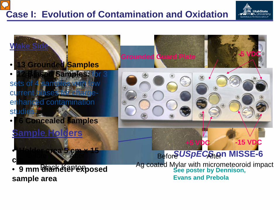
SUSpECS on MISSE-6 See poster by Dennison, Evans and Prebola
Case I: Evolution of Contamination and Oxidation
-15 V
+5 V
Before After Kapton, HN
Before After Ag
Black Kapton Before After Before After
Ag coated Mylar with micrometeoroid impact
+5 VDC
-5 VDC
-15 VDC
Grounded Guard Plate Wake Side • 13 Grounded Samples • 12 Biased Samples: for 3 sets of 4 samples with low current biases for charge-enhanced contamination studies. • 6 Concealed samples Sample Holders • Holder area 5 cm x 15 cm • 9 mm diameter exposed sample area

Diffuse and Specular Reflectivity changes with surface roughness
Case II: Surface Modification
Successive stages of roughened Cu
c.
b.
γ e- γ View photon (electron) scattering as a competition for deposited energy and charge: • Reflectivity—γ out (Luminescence—γ out ) • Photoyield—e out (SE/BSE—e out )

Reflectivity changes with surface roughness and contamination Reflect→Charging→Contamination
Cases I and II: Reflectivity as a Feedback Mechanism
Ground Tests: Threshold Charging vs. Absorption
Solar Probe Mission: Charging vs. Emissivity See Donegan, Sample, Dennison and Hoffmann
JWST Structure: Charging vs. Ablation
Large Breakdown
X:41.583
Y:58.444
Before After Zoomed Images
C
Radiation Damage (Color Change) of Tedlar
B. Mihaljcic in Guild’s 11th SCTS Talk
Charging→ Reflectivity
Radiation → Reflect→Emissivity→Temp→Contamination
Reflect→Emissivity→Temp→Contamination
See Lai & Tautz, 2006 & Dennison 2007

Large Dosage (>108 Rad)
Case III: Radiation Effects
“…auroral fields may cause significant surface charging…” H. Garrett Examples: RBSP, JUNO, JGO/JEO Mechanical and Optical Materials Damage
Medium Dosage (>107 Rad)
Low Dose Rate (>100 Rad/s)
“…Earth is for Wimps…” H. Garrett Examples: RBSP, MMS, JUNO, JGO/JEO Mechanical Modification of Electron Transport and Emission Properties Caused by bondbreaking and trap creation (see Hoffmann & A Sim posters)
(a)
(b)
Examples: Radiation induced Conductivity (RIC) Temperature depndant (see A Sim posters)

Case IV: Temperature Effects
Examples: IR and X-Ray Observatories JWST, WISE, WMAP, Spitzer, Herscel, IRAS, MSX, ISO, COBE, Planck Outer Planetary Mission Galileo, Juno, JEO/JGO. Cassini, Pioneer, Voyager, Inner Planetary Mission SPM, Ulysses, Magellan, Mariner
Strong T Dependence for Insulators
Charge Transport • Conductivity • RIC • Dielectric Constant • ESD

Case IV: Temperature Effects
k(T)
1)( →∆ Tc
cTT
TT +→∆ )(
Uniform Trap Density Exponential Trap Density
230 240 250 260 270 280 290 30038
40
42
44
46
48
50p p y
Temperature (K)
Ln (C
alcu
late
d R
esis
tivty
(Ohm
-cm
))
σVRH~exp(T-¼)σTAH~exp(T-1)
Tt
Strong T Dependence for Insulators
Charge Transport • Conductivity • RIC • Dielectric Constant • ESD

Case IV: Temperature Effects—JWST
Very Low Temperature Virtually all insulators go to infinite resistance—perfect charge integrators Long Mission Lifetime (10-20 yr) No repairs Very long integration times Large Sunshield Large areas Constant eclipse with no photoemission Large Open Structure Large fluxes Minimal shielding
JWST
Variation in Flux Large solar activity variations In and out of magnetotail Complex, Sensitive Hardware Large sensitive optics Complex, cold electronics
Optical Telescope Element (OTE)
Integrated Science Instrument Module (ISIM)
Sunshield
Spacecraft Bus
Warm Sun-facing Side
Cold Space-facing Side
Optical Telescope Element (OTE)
Integrated Science Instrument Module (ISIM)
Sunshield
Spacecraft Bus
Warm Sun-facing Side
Cold Space-facing Side

19
Case V: Temperature and Dose Effects
WideTemperature Range <100 K to >1800 K Wide Dose Rate Range Five orders of magnitude variation!
Wide Orbital Range Earth to Jupiter Flyby Solar Flyby to 4 Rs

20
Case V: Temperature and Dose Effects
“We anticipate significant thermal and charging issues.” J. Sample
• Mission design by APL/GSFC • Materials testing by Dennison and Hoffmann • Evolutionary Charging Study by Donegan, Sample, Dennison & Hoffmann (See Donegann et al, JSR 2009) • Revised mission design and new charging study (See Donegann 11th SCTC Poster for update)
Batch Processing of Evolving Materials Parameters in NASCAP

21
Case V: Temperature and Dose Effects
Wide Dose Rate Range Five orders of magnitude variation!
Wide Orbital Range Earth to Jupiter Flyby Solar Flyby to 4 Rs
WideTemperature Range <100 K to >1800 K

22
TkE
DCoDC
Bo
eT−
= σσ )(
)(
RICRIC )(k (T)T
DTƥ
=σ
)298()( KTT RTr −∆+= εεε
)298()( KTRTESDESD
ESDeETE −−= α
Case V: Temperature and Dose Effects
Dark Conductivity
RIC Electrostatic Breakdown
Dielectric Constant
Dark Conductivity vs T RIC vs T

23
Case V: Temperature and Dose Effects
A peak in charging at ~0.3 to 2 AU “…Curiouser and curiouser…” --Alice

24
Case V: Temperature and Dose Effects
A fascinating trade-off
• Charging increases from increased dose rate at closer orbits • Charge dissipation from T-dependant conductivity increases faster at closer orbits
General Trends Dose rate decreases as ~r-2
T decreases as ~e-r σDC decreases as ~ e-1/T σRIC decreases as ~ e-1/T and decreases as ~r-2

Case VI: Multilayer/Nanocomposite Effects
Length Scale • Nanoscale structure of materials • Electron penetration depth • SE escape depth
Consider the Effects of Multilayer Materials, Composites, Contamination, or Oxidation
Time Scales • Deposition times • Dissipation times • Mission duration
~100 nm SiO2 Coating
~20 nm Conducting Coating
2.54 cm thick fused silica substrate
Grounded
metal
baffle
~200 nm Ag FSS99 Coating
~20 nm Non-conducting Coating
~10 nm Non-conducting Coating #2~10 nm Non-conducting Coating #1
Coated Mirror Structure Power Deposition Graph

Why Does Glow Scale with Flux, Energy and Power?
10 µm
In a simple, but reasonably accurate CSDA, used to model energy loss of electrons traversing solids and their penetration range, the rate of energy loss (dE/dz) is assumed constant. Assuming emission intensity is proportional to energy deposition (dose), emission scales as:
• Incident e-flux, for non-penetrating radiation • Incident power, for penetrating radiation
Emission scaling depends on sample geometry and materials properties. May lead to:
• Power or flux scaling at different incident energies • Energy or flux thresholds and/or cutoffs • Significant emission from high energy e- • Significant emission from back sides or interior surfaces
Kapton

Diversity of Emission Phenomena in Black Kapton
Surface Glow
Relatively low intensity Always present over full surface when e-beam on May decay slowly with time Edge Glow
Similar to Surface Glow, but present only at sample edge “Flare”
2-20x glow intensity Abrupt onset 2-10 min decay time Arc
Relatively very high intensity 10-1000X glow intensity Very rapid <1 us to 1 s
Ball Black Kapton Runs 131 and 131A
110 or 4100 uW/cm2
5 or 188 nA/cm2
Sustained Glow
Arc
1
Flare
Flare
Arc
Arc
Sustained Glow
Sustained Glow Electrometer
CCD Video Camera (400 nm to 900 nm)
InGaAs Video Camera (900 nm to 1700 nm)
2
3 4
1 2
22 keV 135 K

M55J ~4100 uW/cm2
~188 nA/cm2
22 keV 135 K Run 122A
M55J ~110 uW/cm2
~5 nA/cm2
22 keV 135 K Run 122
M55J ~1300 uW/cm2
~188 nA/cm2
7 keV 128 K Run 121A
M55J ~35 uW/cm2
~5 nA/cm2
7 keV 128 K Run 121
Glow Increases with Increasing Flux, Energy and Power
e- Flux
e- Energy
• Surface Glow, Edge Glow, and Arcing Frequency are all found to increase with increasing incident electron flux and energy. • Insufficient data for trends to establish functional dependence and possible thresholds or cut-offs

T300 Glow seen at MSFC Flux density =1 nA/cm2
Energy=22 keV Power 22 uW/cm2 Temp = 296 K and 90 K I90/I296 ~ 4 Similar behavior seen for M55J and Black Kapton
Surface Glow 296 K
Surface Glow 90 K
Emission Increases with Decreasing Temperature
M55J Glow seen at USU Flux density =5 nA/cm2
Energy=22 keV Power 110 uW/cm2 Temp = 294 K and 130 K
Sample Area
Surface Glow 294 K
Surface Glow 130 K
“Flare” 130 K

9/24/12 LANL Seminar 30
𝐼𝐼𝛾𝛾(𝐽𝐽𝑏𝑏 ,𝐸𝐸𝑏𝑏 ,𝑇𝑇, 𝜆𝜆) ∝ �̇�𝐷(𝐽𝐽𝑏𝑏 ,𝐸𝐸𝑏𝑏) � 1�̇�𝐷+�̇�𝐷𝑠𝑠𝑠𝑠𝑠𝑠
� 𝜀𝜀𝑆𝑆𝑇𝑇𝑘𝑘𝐵𝐵𝑇𝑇
�� �𝔸𝔸𝑓𝑓(𝜆𝜆)[1 + ℝ𝑚𝑚 (𝜆𝜆)]� (1)
where dose rate �̇�𝐷 (absorbed power per unit mass) is given by
�̇�𝐷(𝐽𝐽𝑏𝑏 ,𝐸𝐸𝑏𝑏) = 𝐸𝐸𝑏𝑏 𝐽𝐽𝑏𝑏 [1−𝜂𝜂(𝐸𝐸𝑏𝑏 )]𝑞𝑞𝑒𝑒𝜌𝜌𝑚𝑚
× �[1/𝐿𝐿]
[1 𝑅𝑅(𝐸𝐸𝑏𝑏)⁄ ] ; 𝑅𝑅(𝐸𝐸𝑏𝑏) < 𝐿𝐿 ; 𝑅𝑅(𝐸𝐸𝑏𝑏) > 𝐿𝐿
� (2)
Fig. 3.Range and dose rate of disordered SiO2 as a function of incident energy using calculation methods and the continuous slow-down approximation described in [5].
Fig. 2. Qualitative two-band model of occupied densities of state (DOS) as a function of temperature during cathodoluminescence. (a) Modified Joblonski diagram for electron-induced phosphorescence. Shown are the extended state valence (VB) and conduction (CB) bands, shallow trap (ST) states at εST within ~kBT below the CB edge, and two deep trap (DT) distributions centered at εDT=εred and εDT=εblue. Energy depths are exaggerated for clarity. (b) At T≈0 K, the deeper DT band is filled, so that there is no blue photon emission if εblue<εeff. (c) At low T, electrons in deeper DT band are thermally excited to create a partially filled upper DT band (decreasing the available DOS for red photon emission) and a partially empty lower DT band (increasing the available DOS for blue photon emission) (d) At higher T, enhanced thermal excitations further decrease red photon emission and increase blue photon emission. Radiation induced
(a) (c) (b) (d)
Model for Luminescence Intensity in Fused Silica

9/24/12 LANL Seminar 31
Fig. 1. Optical measurements of luminescent thin film disordered SiO2 samples. (a) Three luminescence UV/VIS spectra at decreasing sample temperature. Four peaks are identified: red (~645 nm), green (~500 nm), blue (~455 nm) and UV (275 nm). (b) Peak amplitudes as a function of sample temperature, with baseline subtracted and normalized to maximum amplitudes. (c) Peak wavelength shift as a function of sample temperature. (d) Total luminescent radiance versus beam current at fixed incident energy fit by (1). (e) Total luminescent radiance versus beam energy at fixed incident flux fit by (1). (f) Total luminescent radiance versus beam energy at fixed 10 nA/cm2 incident flux for epoxy-resin M55J carbon composite (red; linear fit), SiO2 coated mirror (green; fit with (1)), and
(d)
(a) (b)
(c)
(e) (f)
Measured Cathodoluminescence Intensity in Fused Silica

Arcs Observed in Black Kapton and M55J
Arc Characteristics
Consecutive frames of discharge event (60 frames/sec)
InGaAs camera (900nm-1700nm)
1 2
3 4
Arc
Arc Electrometer
Arc duration: ~0.2 to 0.8 s in electrometers and video cameras Arc Freq. at 110 µW/cm2 : ~10 arcs/hr for Black Kapton ~30 arcs/hr for M55J Arc Intensity: ~ 10X to1000X glow amplitude ~5% to 20% of glow power CCD camera (400nm-900nm)
Electrometer InGaAs Video CCD Video
Rapid Arcing at 4 mW/cm2
~20000 ars/hr
Ball Black Kapton Runs 131 and 131A
110 or 4100 uW/cm2
5 or 188 nA/cm2 22 keV 135 K
Electrometer

“Flares” Observed in Black Kapton
“Flare” Characteristics
Flare Electrometer
“Flare” duration: Abrupt onset ~2-10 min exp. decay time in electrometers and video cameras “Flare” Freq.uency: 0-2 flares/hr “Flare” Intensity: ~ 2X to20X glow amplitude ~5% to 20% of glow power
CCD camera (400nm-900nm)
Ball Black Kapton Runs 131 110 uW/cm2
5 nA/cm2
22 keV 135 K
InGaAs Video
1 cm
M55J 5 nA/cm2
22 keV 135 K
CCD Camera (RGB) Flare
Flare

7/3/2012 34 USU JWST Progress Report
Details of Electrometer “Flare” Signature
-30
-20
-10
0
Cur
rent
(nA
)
3500300025002000150010005000
Time (s)
Sample nA Sample GND nA Stage nA
Total Beam Time: 3204 s # of Arcs: >50
Two very large arcs with many other small arcs.
Electrometer Data
Flares
Arcs
High Conductivity C-loaded Kapton 25keV 38nA ~1 hr

Conclusions • Complex satellites require:
• Complex materials configurations • More power • Smaller, more sensitive devices • More demanding environments
• There are numerous clear examples where accurate dynamic charging models require accurate dynamic materials properties
• It is not sufficient to use static (BOL or EOL) materials properties
• Enivronment/Materials Modification feedback mechanisms can cause many new problems
• Use available modeling tools with broader materials knowledgebase and a conscious awareness of the dynamic nature of materials to foresee and mitigate potential spacecraft charging problems

9/24/12 LANL Seminar 36
End with a Bang

9/24/12 LANL Seminar 37
Supplemental Slides

9/24/12 LANL Seminar 38
Extremely Low Conductivity
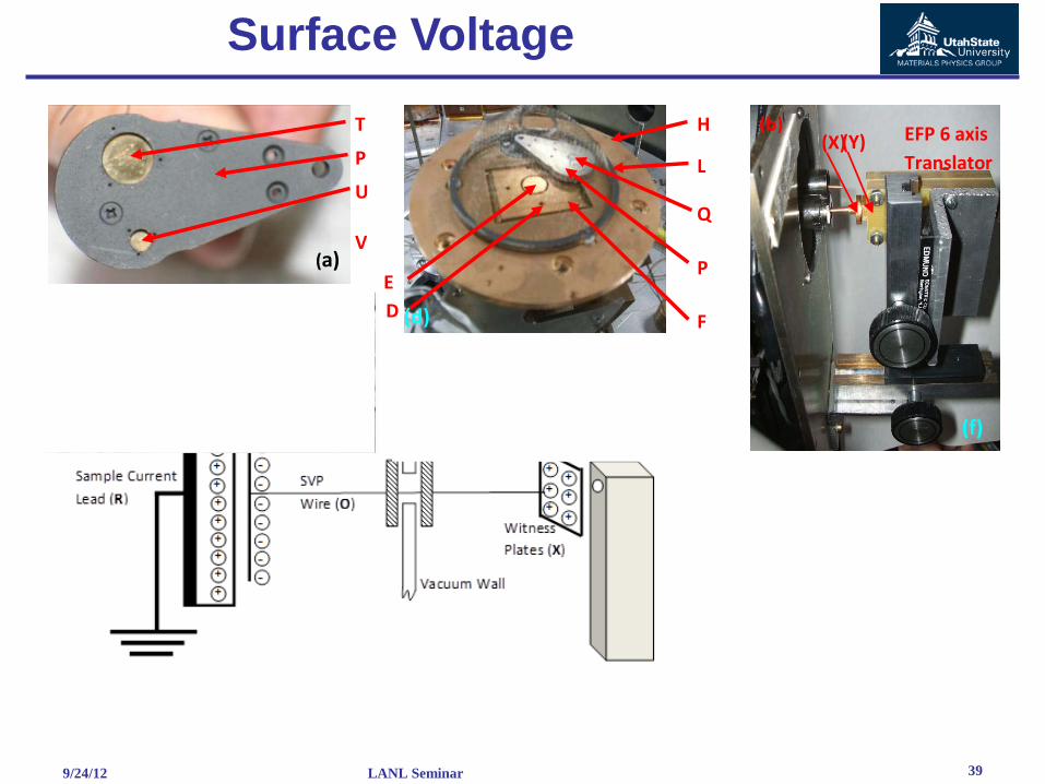
9/24/12 LANL Seminar 39
(X) (Y) EFP 6 axis Translator
(b) T
P
U
V
(a)
(f)
H
L
C
(d) (e) (g) (h)
(d)
H
L
Q
P
F
(b)
D E
Surface Voltage

9/24/12 LANL Seminar 40
F E R C F
T
P Q
S
U
I
I
L K
O M
N
F
D
E
G H
C
I R
Fig. 2. Hemispherical Grid Retarding Field Analyzer (HGRFA). (a) Photograph of sample stage and HGRFA detector (side view). (b) Cross section of HGRFA. (c) Photograph of sample stage showing sample and cooling reservoir. (d) Side view of the mounting of the stepper motor. (e) Isometeric view of the HGRFA detailing the flood gun, optical ports, and wire harness.
(b) (a)
(d) (c) (e)
J
A
E
D
B
A
F

41
Low Charge Capabilities

Luminescence/Arc/Flare Test Configuration
Sample cooled with l-N2 to 100-135 K. Chamber walls at ambient.

• λ range: detectors (700-5500 nm), cameras (400-5000 nm), and spectrometers (200-1700 nm)
• Current range: (0.1 pA to 1 mA)
• Temporal range: <10-9 s to >104 s
Luminescence/Arc/Flare Test Configuration

Comparison of Luminescence Images
10/29/2010 USU JWST Progress Report 44
M55J 1 nA/cm2
22 keV 100 K
“Flare”
Kapton XC 500 nA/cm2
22 keV 150 K
Kapton E 500 nA/cm2
22 keV 150 K
Sustained Glow
Kapton E 5 uA/cm2
22 keV 150 K
IEC Shell Face Epoxy Resin with Carbon Veil
1 nA/cm2
22 keV 100 K
Arcs
1 cm Dia test samples
30 s Exposure SLR Camera (400nm-640nm)
33 ms Exposure CCD Video Camera (500nm-900nm) 17 ms Exposure InGaAs Video Camera (900nm-1700nm)
LaB6 Thermal Spot M55J 1 nA/cm2
22 keV 100 K
M55J 5 nA/cm2
22 keV 135 K
IEC Shell Face Epoxy Resin with Carbon Veil
1 nA/cm2
22 keV 100 K
IEC Shell Face Epoxy Resin with Carbon Veil
5 nA/cm2
22 keV 100 K
Kapton XC 50 nA/cm2
22 keV 150 K
Kapton XC 5 nA/cm2
22 keV 1350 K
Arc

9/24/12 LANL Seminar 45
Electrostatic Breakdown

Impi
ngin
g on
a Flat
Sur
face
Use or disclosure of data contained on this page is subject to the restriction(s) on the title page of this document. 46
EV Spec worst case (Minow)
These values are 10 x the model input values, adjusted in the model per recent Geotail and WIND data
Hofmeister plot

Sample 275XC/Kevlar/275XC cross section view
Ball Kapton/Kevlar Composite—SEM Inspection (GSFC)

Sample 275XC/Kevlar/275XC cross section view
Ball Kapton/Kevlar Composite—SEM Inspection (GSFC)