Embed Size (px)
Citation preview

The Development of an Ionization Profile Monitor for use in the Tevatron
Lawrence Short BullSJSU, San Jose, CA
Supervisor: Andreas Jansson Beams Division, FNAL
SIST Summer 2003

Agenda
Introduction Principles of Operation Design Details Experiments Conclusion Acknowledgements

Introduction
Quantities of InterestLuminosityEmittance
Emittance Monitoring Devices at FNALFlying WireSynchrotron Light Monitor Ionization Profile Monitor (IPM)

Luminosity
Run II Goals: peak L 5.1E31 cm^-1sec^-1, integrated 2fb^-1
Emittance
projection onto x/y axis provides transverse beam dist. r.m.s. value of beam density distribution provides
measure of beam size Beam size given as r.m.s of Gaussian beam profiles Initial distribution not quite Gaussian, by time final
energy reached is very good approximation.
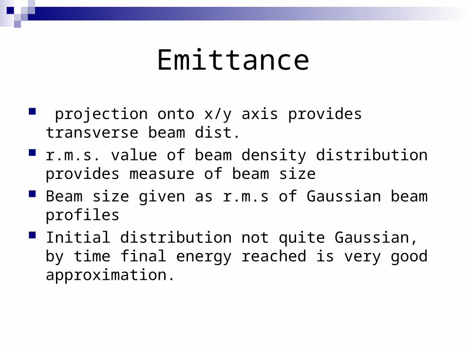
Emittance monitoring in Tevatron
Flying Wires Evasive diagnostic tool
Synchrotron Light Monitor Non-evasive
Reported emittances show discrepancy Potential emittance monitoring in Tev
IPM Schottky Detector

Why an IPM for the Tev?
Run II Instrumentation Motivations Transverse and longitudinal emittance
preservation Real time operational tuning & monitoring
Tev IPM provides turn-by-turn profile measurements for transverse injection matching
Sync lite only “on-line” transverse profile monitor available during store (insuff. Light @ 150 Gev)
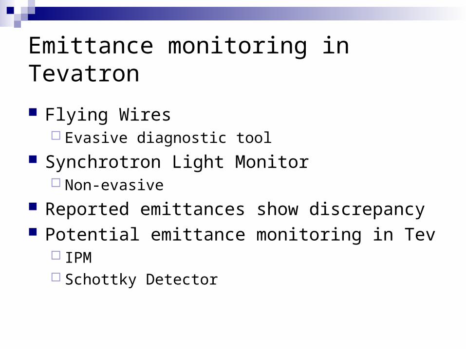
IPM Fundamentals
Provide transverse beam profiles: vertical & horizontal Residual gas ionization occurs with each bunch passage Collection of ions/electrons with electric clearing field Combat space charge effects Utilizes microchannel plate(MCP) for charge multipliction Amplified signal of charge collected on anode strip Signal integrated, amplified, and digitized Sent from memory to processor to provide histogram
profiles
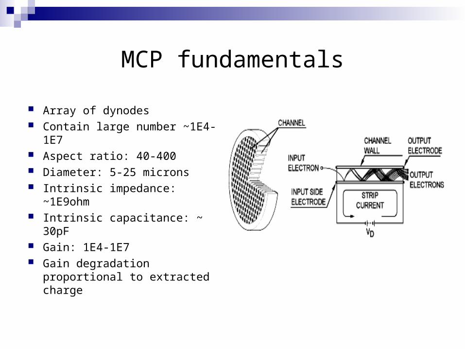
MCP fundamentals
Array of dynodes Contain large number ~1E4-
1E7 Aspect ratio: 40-400 Diameter: 5-25 microns Intrinsic impedance: ~1E9ohm Intrinsic capacitance: ~ 30pF Gain: 1E4-1E7 Gain degradation proportional
to extracted charge
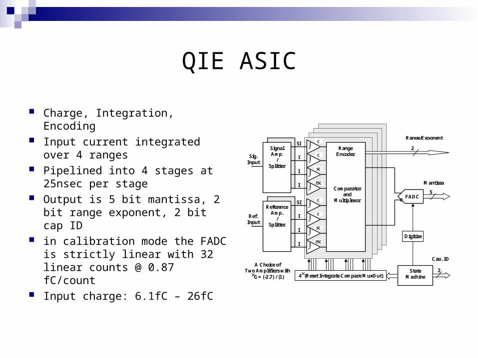
QIE ASIC
Charge, Integration, Encoding Input current integrated over 4
ranges Pipelined into 4 stages at
25nsec per stage Output is 5 bit mantissa, 2 bit
range exponent, 2 bit cap ID in calibration mode the FADC
is strictly linear with 32 linear counts @ 0.87 fC/count
Input charge: 6.1fC – 26fC
5I
I
I
I
Signal Amp.
/ Splitter
5I
I
I
I
ReferenceAmp.
/ Splitter
Comparator and
Multiplexor
Sig. Input
Ref. Input
Range Encoder
FADC
C
C
5C
25C
C
C
5C
25C
State Machine 4(Reset Integrate Compare MuxOut)
Digitize
Mantissa
Range/Exponent
Cap. ID
2
2
5
A Choice of Two Amplifiers with
G= (-2.7) / (1)

1 2 3 4 5 6 7 8 9101112131415161718192021222324252627282930313233
10
20
30
40
50
E B
Anode strips
Beam
MCP
Tev IPM Design 36 X 36 proton and pbar bunches Time between bunches ~396ns Bunch length ~ 3ns r.m.s., 18-20ns Only ~1000 e liberated during
ionization Electronics must be low noise Need Faraday screen to protect
detector from image current @ 53MHz
Pull only signal through vacuum flange, reference terminated @ vacuum
Anode to ground completely floating
screen

Block diagram/data flow chart
seri
aliz
er
16 serial links(optical fiber)~1.6 Gbits/s/link~23 Gbit/s total
Sam
ple
cloc
k (1
7.6
MH
z)
Ano
de s
tirp
sig
nals
(~1
28)
16
Proton revolution marker
Kwame Vince, Mark et al
PCIX busDMA xferBurst mode~1 Gbit/s
Pbar revolution markerQ
IEQ
IE(8
QIE
s)
opti
cal d
rive
r
Fas
t (w
ide)
mem
ory
FP
GA Data
Hea
der
byte
QIE
res
et
QIE
mod
e
Header card53 MHz RF
Timing card Injection eventoff-the-shelf
in tunnel in upstairs PC
GPIB controller
To power supplies
PC
I B
US

MI IPM Studies
Utilized IPMM1H & IPMM2H Investigate effects of a varying bias
voltage for MCP in detectors ACNET variables I:HxMCPV,
I:HxPMEM[ ] ,I:HxPMSG[ ] datalogged at node TevJA
Settings on LabView interface determine what turn number was datalogged
Two ranges were studied
IMPM1H
IPMM2H

MI_IPM: H1 results
1150
2350
950
1050 11
25 1200 12
75
0
10
20
30
40
50
Emittance
turn
MCP_V
H1 IPM: turn vs. MCP_V vs. emit
40-50
30-40
20-30
10-20
0-10
H1 IPM: MC_ V vs. Emittance array
0
5
10
15
20
25
30
35
40
45
50
750 850 950 1050 1150 1250 1350
MCP_V (vol ts)
1000
1150
1300
1600
1750
1900
2050
2200
2350
2650
2800
2950
3100
3250
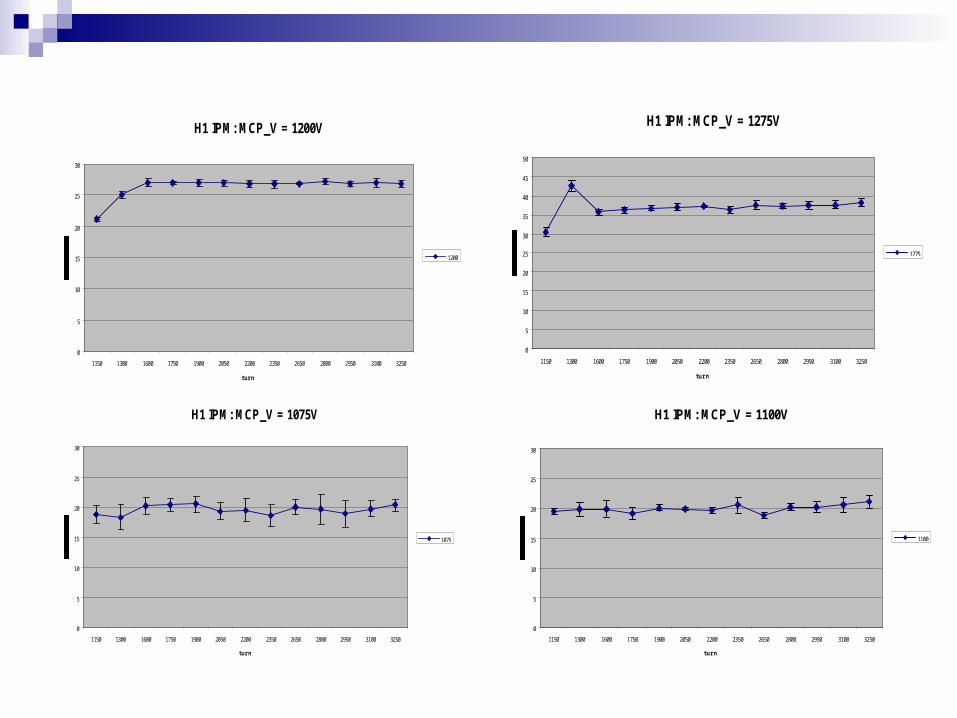
H1 IPM: MCP_V = 1200V
0
5
10
15
20
25
30
1150 1300 1600 1750 1900 2050 2200 2350 2650 2800 2950 3100 3250
turn
1200
H1 IPM: MCP_V = 1275V
0
5
10
15
20
25
30
35
40
45
50
1150 1300 1600 1750 1900 2050 2200 2350 2650 2800 2950 3100 3250
turn
1275
H1 IPM: MCP_V = 1075V
0
5
10
15
20
25
30
1150 1300 1600 1750 1900 2050 2200 2350 2650 2800 2950 3100 3250
turn
1075
H1 IPM: MCP_V = 1100V
0
5
10
15
20
25
30
1150 1300 1600 1750 1900 2050 2200 2350 2650 2800 2950 3100 3250
turn
1100

MI_IPM: H2 resultsH2 IPM: MCP_V vs Emmittance array
0
5
10
15
20
25
30
35
40
45
50
1175 1225 1275 1325 1375 1425
volts
Emm
ittan
ce
[0]
[25]
[50]
[100]
[125]
[150]
[175]
[200]
[225]
[275]
[300]
[325]
[350]
[375]
1000
1300
1750
2050
2350
2800
3100
1200
1225
1250
1275
1300
1325
1350
1375
1400
0
5
10
15
20
25
30
35
40
Emittance
turn
MCP_V
H2 IPM: turn vs MCP_V vs emit
35-40
30-35
25-30
20-25
15-20
10-15
5-10
0-5
1000
1300
1750
2050
2350
2800
3100
1200
1225
1250
1275
1300
1325
1350
1375
1400
0
5
10
15
20
25
30
deviation
turn
MCP_V
H2 IPM: turn vs. MCP_V vs. deviation
25-30
20-25
15-20
10-15
5-10
0-5

H2 IPM: MCP_V = 1400V
0
5
10
15
20
25
30
35
40
1000 1150 1300 1600 1750 1900 2050 2200 2350 2650 2800 2950 3100 3250
turn
Em
mit
tan
ce
1400
H2 IPM: MCP_V = 1300V
0
5
10
15
20
25
30
35
40
1000 1150 1300 1600 1750 1900 2050 2200 2350 2650 2800 2950 3100 3250
turn
Em
mit
tan
ce
1300

H2 IPM: MCP_V vs. Emit array
0
5
10
15
20
25
30
35
40
45
50
1270 1280 1290 1300 1310 1320 1330
volts
Em
mit
tan
ce
1000
1150
1300
1600
1750
1900
2050
2200
2350
2650
2800
2950
3100
3250
MI_IPM: H2 better resolution
1000
1600
2050
2650
3100
1275 1280
1285
1290 1295
1300
1305
1310
1315
1320
1325
0
5
10
15
20
25
30
35
Emmittance
turn
MCP_V
H2 IPM:turn vs. MCP_V vs. emit
30-35
25-30
20-25
15-20
10-15
5-10
0-51000
1600
2050
2650
3100
1275 1280 1285 1290 1295
1300 1305 1310
1315
1320 1325
0
1
2
3
4
5
6
deviation
turn
MCP_V
H2 IPM: turn vs. MCP_V vs. deviation
5-6
4-5
3-4
2-3
1-2
0-1

H2 IPM: MCP_V = 1295V
0
5
10
15
20
25
30
35
1000 1150 1300 1600 1750 1900 2050 2200 2350 2650 2800 2950 3100 3250
turn
Em
mit
tan
ce
1295
H2 IPM:MCP_V = 1300V
0
5
10
15
20
25
30
35
1000 1150 1300 1600 1750 1900 2050 2200 2350 2650 2800 2950 3100 3250
turn
Em
mit
tan
ce
1300
H2 IPM: MCP_V = 1325V
0
5
10
15
20
25
30
35
1000 1150 1300 1600 1750 1900 2050 2200 2350 2650 2800 2950 3100 3250
turn
Em
mit
tan
ce
1325
H2 IPM: MCP_V = 1320V
0
5
10
15
20
25
30
35
1000 1150 1300 1600 1750 1900 2050 2200 2350 2650 2800 2950 3100 3250
turn
Em
mit
tan
ce
1320

MI_IPM: H2 up the rampH2 IPM : MCP_V vs. Emit array
0
20
40
60
80
100
120
1175 1225 1275 1325 1375 1425
vol ts
20
4445
8870
17720
22145
26570
30995
35420
39845
48695
53120
57545
61970
66395 20
2214
5
3984
5
6197
012
00 1285 13
10 1375
02040
60
80
100
120
140
Emmittance
tur n
MCP_V
H2 IPM: turn vs. MCP_V vs. emit
120-140
100-120
80-100
60-80
40-60
20-40
0-20
H2 IPM: MCP_V = 1295V
0
10
20
30
40
50
2044
4588
70
1772
0
2214
5
2657
0
3099
5
3542
0
3984
5
4869
5
5312
0
5754
5
6197
0
6639
5
tur n
1295
H2 IPM: MCP_V = 1300V
0
10
20
30
40
50
60
2044
4588
70
1772
0
2214
5
2657
0
3099
5
3542
0
3984
5
4869
5
5312
0
5754
5
6197
0
6639
5
turn
1300

QIE Noise Measurements The noise floor of the CKM QTBB floor was determined Noise for various cable configurations was to be determined
Data Multiplexing
QIE A
QIE B
16 bit SERDES w/ 8B/10B
Clock dist. ckt. 40MHz

QIE A: noise floor
0
500
1000
1500
2000
2500
3000
3500
4000
4500
5000
1 2 3 4 5 6 7 8 9 10 11 12 13 14 15 16 17 18 19 20 21 22 23 24 25 26 27 28 29 30M
ore
Bin
Fre
qu
ency
Frequency
Pedestal = 19.481 r.m.s = 0.6919
Noise floor channel A: input impedance = 50 ohm

Noise floor per cap ID: input impedance = 50 ohm
0
200
400
600
800
1000
1200
1400
1600
1 2 3 4 5 6 7 8 9 10 11 12 13 14 15 16 17 18 19 20 21 22 23 24 25 26 27 28 29 30M
ore
Bin
Fre
qu
ency
Frequency
0
200
400
600
800
1000
1200
1400
1 2 3 4 5 6 7 8 9 10 11 12 13 14 15 16 17 18 19 20 21 22 23 24 25 26 27 28 29 30M
ore
Bin
Fre
qu
ency
Frequency
0
200
400
600
800
1000
1200
1400
1600
1 2 3 4 5 6 7 8 9 10 11 12 13 14 15 16 17 18 19 20 21 22 23 24 25 26 27 28 29 30M
ore
Bin
Fre
qu
ency
Frequency
0
200
400
600
800
1000
1200
1400
1 2 3 4 5 6 7 8 9 10 11 12 13 14 15 16 17 18 19 20 21 22 23 24 25 26 27 28 29 30M
ore
Bin
Fre
qu
ency
Frequency
Cap ID 0 Cap ID 1
Cap ID 2 Cap ID 3
r.m.s = 0.6647 r.m.s = 0.6642
r.m.s = 0.6709 r.m.s = 0.6814

calibration mode: gain factor
0
5
10
15
20
25
-4 -2 0 2 4 6 8 10 12 14
injected charge (fC)
ou
tpu
t b
in
cap id 0
cap id 1
cap id 2
cap id 3 noise, e- gain factor
cap id 0 3152 0.7598
cap id 1 3142 0.7579
cap id 2 3158 0.7540
cap id 3 3232 0.7598
Gain factor for channel: 0.7579
Noise for channel: 3171e
Determination of Gain Factor per cap ID: Zin = 50 ohm

QIE_A: capacitance in signal input only
0
0.5
1
1.5
2
2.5
0 50 100 150 200 250 300 350
input capacitance (pF)
RM
S (
cou
nts
)
cap_id 0
cap_id 1
cap_id 2
cap_id 3
QIE_A: capacitance to refrence input only
0
0.5
1
1.5
2
2.5
0 50 100 150 200 250 300 350
input cap. (pF)R
MS
(cn
ts)
cap_id 0
cap_id 1
cap_id 2
cap_id 3
Capacitance input to either signal or reference inputs
Peculiar behavior displayed, further investigation required

QIE_A: capacitance to both inputs
0
0.5
1
1.5
2
2.5
0 50 100 150 200 250 300 350
input cap. (pF)
RM
S (
cnts
)
cap_id 0
cap_id 1
cap_id 2
cap_id 3
QIE_A: calcualted noise
0
1000
2000
3000
4000
5000
6000
7000
8000
9000
0 50 100 150 200 250 300
input cap (pF)el
ectr
on
s cap id 0
cap id 1
cap id 2
cap id 3
Configuration of interest: input cap. To both signal & reference
Noise levels appear within tolerances for design

Noise floor channel A: input impedance = 93 ohm
QIE A: noise floor
0
1000
2000
3000
4000
5000
6000
1 2 3 4 5 6 7 8 9 10 11 12 13 14 15 16 17 18 19 20 21 22 23 24 25 26 27 28 29 30M
ore
Bin
Fre
qu
ency
Frequency
Pedestal = 12.7432 r.m.s. = 0.6848
Similar results as 50 ohm case when individual cap id’s examined

Determination of Gain Factor per cap ID: Zin = 93 ohm
Noise for channel: 3123e
Gain factor for channel: 0.7571
noise egain factor
cap id 0 3132 0.7605
cap id 1 2996 0.7588
cap id 2 3141 0.7499
cap id 3 3221 0.7592
input impead. = 93 ohm
0
5
10
15
20
25
30
-10 -8 -6 -4 -2 0 2 4 6 8
input charge (fC)
ou
tpu
t (b
in)
cap_id 0
cap_id 1
cap_id 2
cap_id 3
Less noise, relatively the same gain factor for the channel than the 50 ohm setting

ict: 93
0
500
1000
1500
2000
2500
3000
1 2 3 4 5 6 7 8 9 10 11 12 13 14 15 16 17 18 19 20 21 22 23 24 25 26 27 28 29 30M
ore
Bin
Fre
qu
ency
Frequency
ntd: 50
0
200
400
600
800
1000
1200
1400
1600
1800
2000
1 2 3 4 5 6 7 8 9 10 11 12 13 14 15 16 17 18 19 20 21 22 23 24 25 26 27 28 29 30M
ore
Bin
Fre
qu
ency
Frequency
Cable Test
100 ohm twisted pair cable connected to both signal and reference
Length of cable = 3.75 m Shield of each cable
connected Return for each cable
connected Zin = 93 ohm, noise is
6,808 e Zin = 50 ohm, noise is
10,844 e
Zin = 93 ohm
Zin = 50 ohm

Conclusion Emittance as reported by IPM very sensitive to output
current; N2 leak must be added with care, low gain MCP MCP test stand will be used to study MCP properties for
this project in addition to future projects. Also to diagnose MCP’s coming out of the machine
If QIE noise results correct, good thing. Seem slightly low.
Tev IPM up for technical DOE review in Oct., things look good and will more than likely be commissioned
Encouraging to see CMS & Beams Div. Collaborating on project
FNAL is a rocking place to work

Acknowledgements
I would like to thank Andreas Jansson, Claudio Rivetta, Hogan Nyugen, Jim Zagel, Kwamie Bowie, Dianne Engram, Elliot McCrory, Dr. Davenport and rest of SIST committee.
The 2003 SIST summer interns