Embed Size (px)
Citation preview

The Design Warrior’s Guide to FPGAsDevices, Tools, and Flows. ISBN 0750676043
Copyright © 2004 Mentor Graphics Corp. (www.mentor.com)
1945 1950 1955 1960 1965 1970 1975 1980 1985 1990 1995 2000
FPGAs
ASICs
CPLDs
SPLDs
Microprocessors
SRAMs & DRAMs
ICs (General)
Transistors
Technology timeline (dates are approximate)
1947 -- The first transistor: a point-contact device formed from (Ge).1950 -- Bipolar junction transistor (BJT) silicon (Si) Germanium (Ge)
The Design Warrior’s Guide to FPGAsDevices, Tools, and Flows. ISBN 0750676043
Copyright © 2004 Mentor Graphics Corp. (www.mentor.com)
1962 -- Metal-oxide semiconductor field-effect transistors (MOSFETs); cheaper, smaller, and used substantially less power. There are two main types of FETs, called NMOS and PMOS. Logic gates formed from NMOS and PMOS transistors connected together in a complementary manner are known as a complementary metal-oxide semiconductor (CMOS).
Integrated circuits
1958 -- Texas Instruments (TI): A phase-shift oscillator comprising five components on a singlepiece of semiconductor.
During the mid-1960s -- TI introduced a large selection of basic building block ICs called the 54xx (“fifty-four hundred”) series and the 74xx (“seventy-four hundred”) series, which were specified for military and commercial use.
These “jelly bean” devices, which were typically around 3/4“ long, 3/8" wide, and had 14 or 16 pins, each contained small amounts of simple logic. 74004, 2-input NAND gates, 7402 4, 2-input NOR gates, 7404 6, NOT (inverter) gates.
TI’s 54xx and 74xx series were implemented in TTL.
1968 -- RCA introduced a somewhat equivalent CMOS-based library of parts called the 4000 (“four thousand”) series.
The Design Warrior’s Guide to FPGAsDevices, Tools, and Flows. ISBN 0750676043
Copyright © 2004 Mentor Graphics Corp. (www.mentor.com)
SRAMs, DRAMs, and microprocessors
1970 -- Intel announced the first 1024-bit DRAM (the 1103) and Fairchild introduced the first 256-bit SRAM (the 4100).1971 -- Intel introduced the world’s first microprocessor (μP)—the 4004. Also referred to as a “computer-on-a-chip,” the 4004 contained only around 2,300 transistors and could execute60,000 operations per second.
Today’s FPGAs are SRAM-based, and some of today’s high-end devices incorporate embedded microprocessor cores.
The Design Warrior’s Guide to FPGAsDevices, Tools, and Flows. ISBN 0750676043
Copyright © 2004 Mentor Graphics Corp. (www.mentor.com)
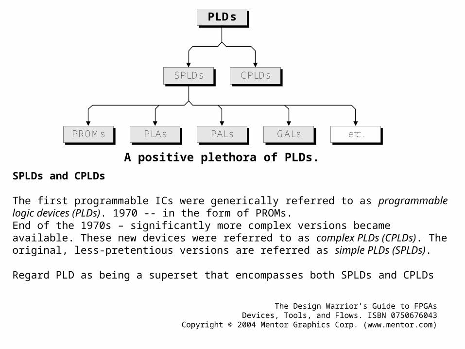
PLDs
SPLDs CPLDs
PLAsPROMs PALs GALs etc.
SPLDs and CPLDs
The first programmable ICs were generically referred to as programmable logic devices (PLDs). 1970 -- in the form of PROMs.End of the 1970s – significantly more complex versions became available. These new devices were referred to as complex PLDs (CPLDs). The original, less-pretentious versions are referred as simple PLDs (SPLDs).
Regard PLD as being a superset that encompasses both SPLDs and CPLDs
A positive plethora of PLDs.

The Design Warrior’s Guide to FPGAsDevices, Tools, and Flows. ISBN 0750676043
Copyright © 2004 Mentor Graphics Corp. (www.mentor.com)
a b c
l l l
Address 0 &
Address 1 &
Address 2 &
Address 3 &
Address 4 &
Address 5 &
Address 6 &
Address 7 &
a !a b !b c !c
!a !c!b& &
!a c!b& &
!a !cb& &
!a cb& &
a !c!b& &
a c!b& &
a !cb& &
a cb& &
Predefined AND array
Pro
gram
mab
le O
R a
rray
w x y
Predefined linkProgrammable link
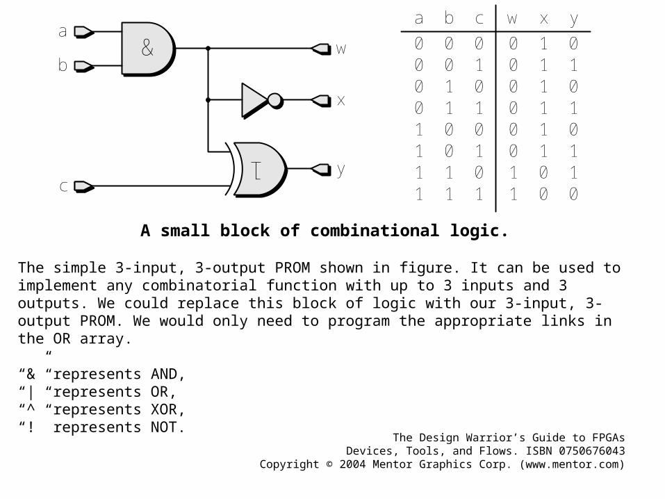
Unprogrammed PROM(predefined AND array, programmable OR array).
The first of the simple PLDs were PROMs, which appeared in 1970.
Consider them as consisting of a fixed array of AND functions driving a programmable array of OR functions. For example, consider a 3-input, 3-output PROM
The Design Warrior’s Guide to FPGAsDevices, Tools, and Flows. ISBN 0750676043
Copyright © 2004 Mentor Graphics Corp. (www.mentor.com)
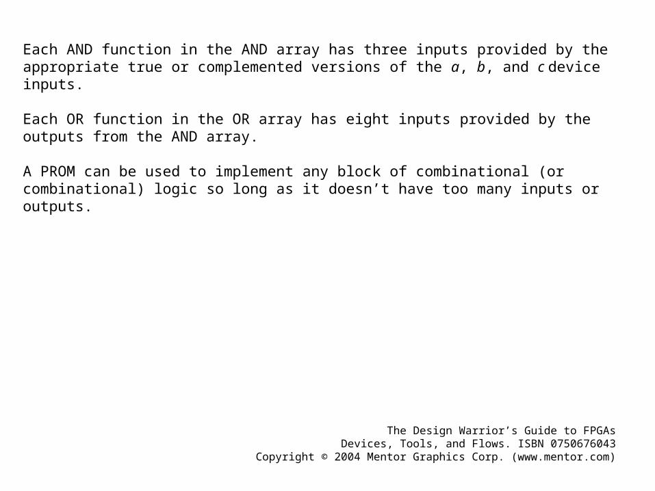
Each AND function in the AND array has three inputs provided by the appropriate true or complemented versions of the a, b, and c device inputs.
Each OR function in the OR array has eight inputs provided by the outputs from the AND array.
A PROM can be used to implement any block of combinational (or combinational) logic so long as it doesn’t have too many inputs or outputs.
The Design Warrior’s Guide to FPGAsDevices, Tools, and Flows. ISBN 0750676043
Copyright © 2004 Mentor Graphics Corp. (www.mentor.com)
a b c w x y
0 0 0 0 1 00 0 1 0 1 10 1 0 0 1 00 1 1 0 1 11 0 0 0 1 01 0 1 0 1 11 1 0 1 0 11 1 1 1 0 0
l
&a
b
c
w
x
y
A small block of combinational logic.
The simple 3-input, 3-output PROM shown in figure. It can be used to implement any combinatorial function with up to 3 inputs and 3 outputs. We could replace this block of logic with our 3-input, 3-output PROM. We would only need to program the appropriate links in the OR array.
“&” represents AND, “|” represents OR, “^” represents XOR, “!” represents NOT.
The Design Warrior’s Guide to FPGAsDevices, Tools, and Flows. ISBN 0750676043
Copyright © 2004 Mentor Graphics Corp. (www.mentor.com)
a b c
l l l
Address 0 &
Address 1 &
Address 2 &
Address 3 &
Address 4 &
Address 5 &
Address 6 &
Address 7 &
a !a b !b c !c
!a !c!b& &
!a c!b& &
!a !cb& &
!a cb& &
a !c!b& &
a c!b& &
a !cb& &
a cb& &
Predefined AND array
Pro
gram
mab
le O
R a
rray
w x y
Predefined linkProgrammable link
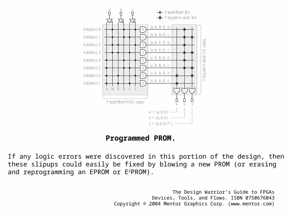
w = (a & b)
x = !(a & b)
y = (a & b) ^ c
Programmed PROM.
If any logic errors were discovered in this portion of the design, then these slipups could easily be fixed by blowing a new PROM (or erasing and reprogramming an EPROM or E2PROM).

The Design Warrior’s Guide to FPGAsDevices, Tools, and Flows. ISBN 0750676043
Copyright © 2004 Mentor Graphics Corp. (www.mentor.com)
a b c
&
&
&
a !a b !b c !c
N/A
Predefined AND array
Pro
gra
mm
able
OR
arr
ay
Predefined linkProgrammable link
l l lw x y
N/A
N/A
Unprogrammed PLA(programmable AND and OR arrays).
PLAsThese were the most user configurable of the simple PLDs because both the AND and OR arrays were programmable. Unlike a PROM, the number of AND functions in the AND array is independent of the number of inputs to the device. Additional ANDs can be formed by simply introducing more rows into the array. Similarly, the number of OR functions in the OR array is independent of both the number of inputs to the device and the number of AND functions in the AND array.
The Design Warrior’s Guide to FPGAsDevices, Tools, and Flows. ISBN 0750676043
Copyright © 2004 Mentor Graphics Corp. (www.mentor.com)
a b c
&
&
&
a !a b !b c !c
a cb& &
a c&
!b !c&
Predefined AND array
Pro
gra
mm
able
OR
arr
ay
Predefined linkProgrammable link
l l l
w x y
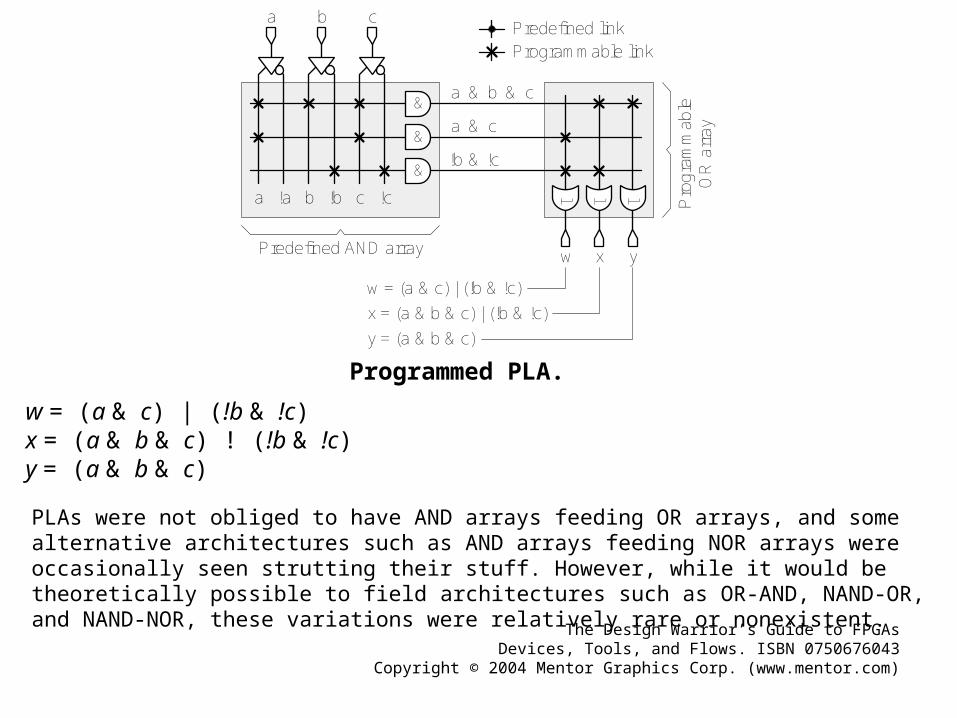
w = (a & c) | (!b & !c)
x = (a & b & c) | (!b & !c)
y = (a & b & c)
Programmed PLA.
w = (a & c) | (!b & !c)x = (a & b & c) ! (!b & !c)y = (a & b & c)
PLAs were not obliged to have AND arrays feeding OR arrays, and some alternative architectures such as AND arrays feeding NOR arrays were occasionally seen strutting their stuff. However, while it would be theoretically possible to field architectures such as OR-AND, NAND-OR, and NAND-NOR, these variations were relatively rare or nonexistent.
The Design Warrior’s Guide to FPGAsDevices, Tools, and Flows. ISBN 0750676043
Copyright © 2004 Mentor Graphics Corp. (www.mentor.com)
a b c
l l l
&
&
&
&
&
&
a !a b !b c !c
ProgrammableAND array
Pre
defin
ed O
R a
rray
w x y
Predefined linkProgrammable link
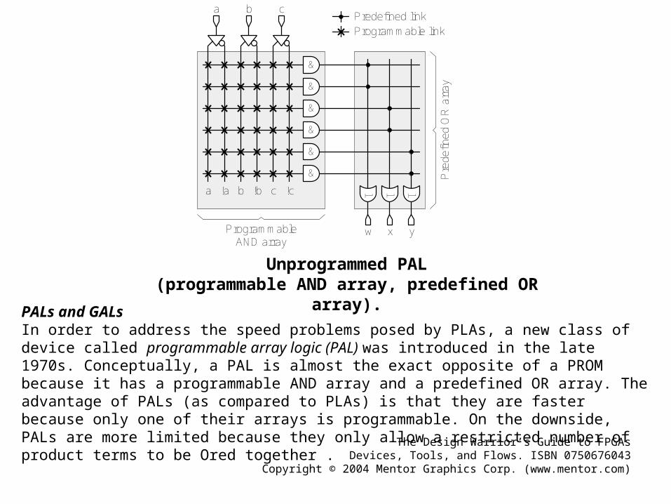
Unprogrammed PAL(programmable AND array, predefined OR array).
PALs and GALsIn order to address the speed problems posed by PLAs, a new class of device called programmable array logic (PAL) was introduced in the late 1970s. Conceptually, a PAL is almost the exact opposite of a PROM because it has a programmable AND array and a predefined OR array. The advantage of PALs (as compared to PLAs) is that they are faster because only one of their arrays is programmable. On the downside, PALs are more limited because they only allow a restricted number of product terms to be Ored together .
The Design Warrior’s Guide to FPGAsDevices, Tools, and Flows. ISBN 0750676043
Copyright © 2004 Mentor Graphics Corp. (www.mentor.com)
ProgrammableInterconnect
matrix
Input/output pinsSPLD-like
blocks
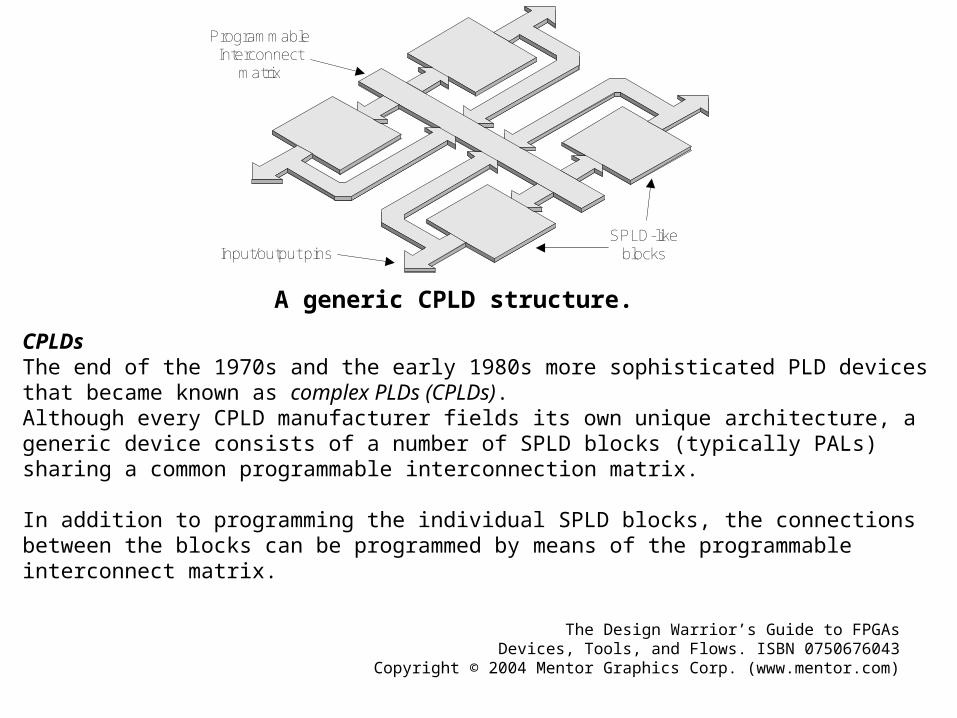
A generic CPLD structure.
CPLDsThe end of the 1970s and the early 1980s more sophisticated PLD devices that became known as complex PLDs (CPLDs).Although every CPLD manufacturer fields its own unique architecture, a generic device consists of a number of SPLD blocks (typically PALs) sharing a common programmable interconnection matrix.
In addition to programming the individual SPLD blocks, the connections between the blocks can be programmed by means of the programmable interconnect matrix.
The Design Warrior’s Guide to FPGAsDevices, Tools, and Flows. ISBN 0750676043
Copyright © 2004 Mentor Graphics Corp. (www.mentor.com)
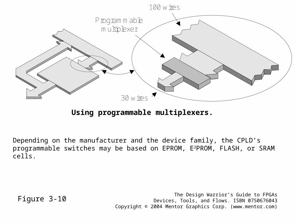
100 wires
30 wires
Programmablemultiplexer
Figure 3-10
Using programmable multiplexers.
Depending on the manufacturer and the device family, the CPLD’s programmable switches may be based on EPROM, E2PROM, FLASH, or SRAM cells.
The Design Warrior’s Guide to FPGAsDevices, Tools, and Flows. ISBN 0750676043
Copyright © 2004 Mentor Graphics Corp. (www.mentor.com)
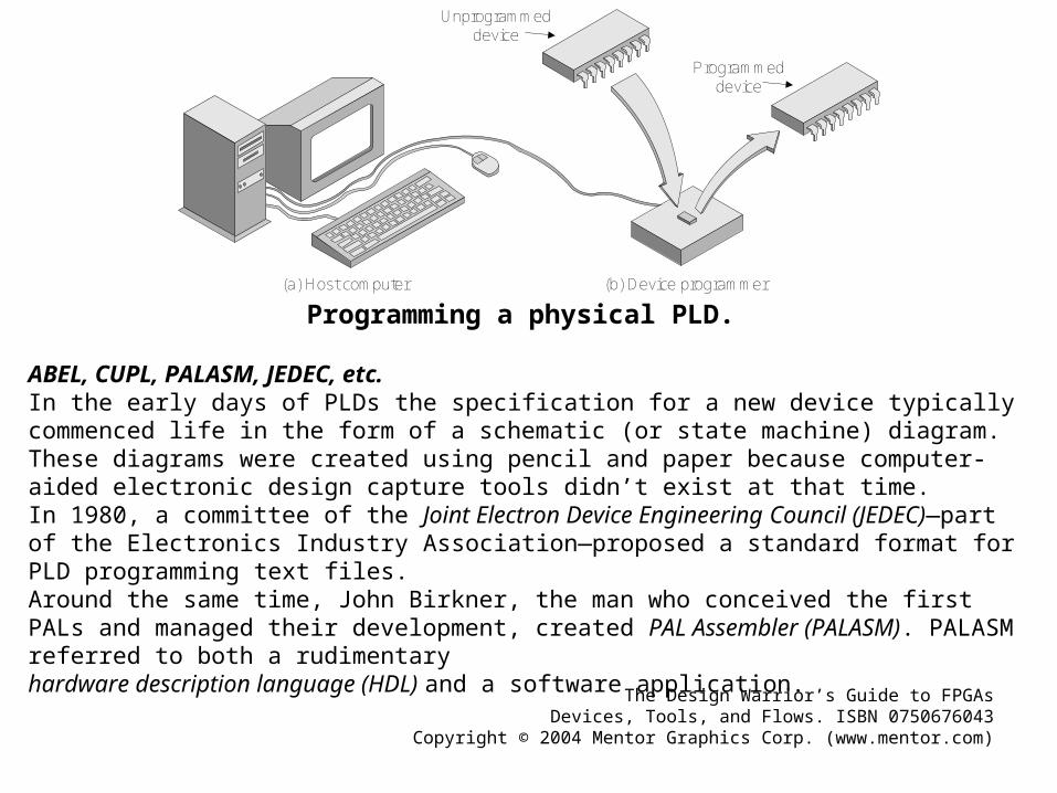
(a) Host computer (b) Device programmer
Unprogrammeddevice
Programmeddevice
ABEL, CUPL, PALASM, JEDEC, etc.In the early days of PLDs the specification for a new device typically commenced life in the form of a schematic (or state machine) diagram. These diagrams were created using pencil and paper because computer-aided electronic design capture tools didn’t exist at that time.In 1980, a committee of the Joint Electron Device Engineering Council (JEDEC)—part of the Electronics Industry Association—proposed a standard format for PLD programming text files. Around the same time, John Birkner, the man who conceived the first PALs and managed their development, created PAL Assembler (PALASM). PALASM referred to both a rudimentaryhardware description language (HDL) and a software application.
Programming a physical PLD.
The Design Warrior’s Guide to FPGAsDevices, Tools, and Flows. ISBN 0750676043
Copyright © 2004 Mentor Graphics Corp. (www.mentor.com)
PALASM only supported PAL devices made by MMI, and it didn’t perform any minimization or optimization. In order to address these issues, Data I/O released its Advanced Boolean Expression Language (ABEL) in 1983. Around the same time, Assisted Technology released its Common Universal tool for Programmable Logic (CUPL). Although PALASM, ABEL, and CUPL are the best known of the early HDLs, there were many others, such as Automated Map and Zap of Equations (AMAZE) from Signetics. These simple languages and associated tools paved the way for the higher-level HDLs (such as Verilog and VHDL) and tools (such as logic synthesis) that are used for today’s ASIC and FPGA designs.

The Design Warrior’s Guide to FPGAsDevices, Tools, and Flows. ISBN 0750676043
Copyright © 2004 Mentor Graphics Corp. (www.mentor.com)
ASICs
StructuredASICs
GateArrays
StandardCell
FullCustom
Increasing complexity
Different types of ASIC.
ASICs (gate arrays, etc.)Four main classes of application specific integrated circuit (ASIC) deserve mention. In increasing order of complexity, these are gate arrays, structured ASICs, standard cell devices, and full-custom chips
The Design Warrior’s Guide to FPGAsDevices, Tools, and Flows. ISBN 0750676043
Copyright © 2004 Mentor Graphics Corp. (www.mentor.com)
LUT
LUT
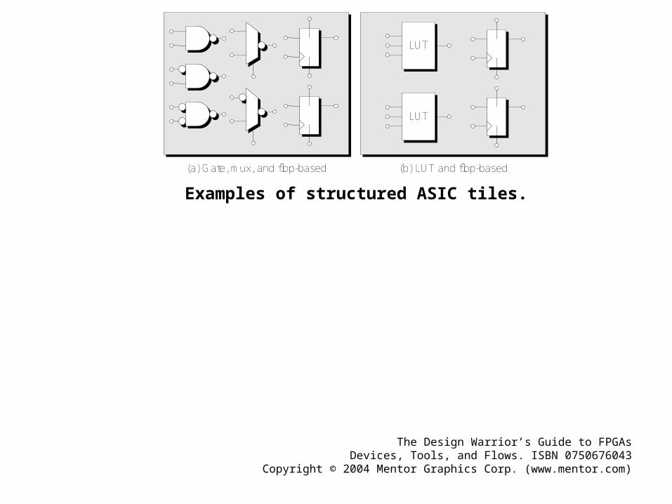
(a) Gate, mux, and flop-based (b) LUT and flop-based
Examples of structured ASIC tiles.
The Design Warrior’s Guide to FPGAsDevices, Tools, and Flows. ISBN 0750676043
Copyright © 2004 Mentor Graphics Corp. (www.mentor.com)
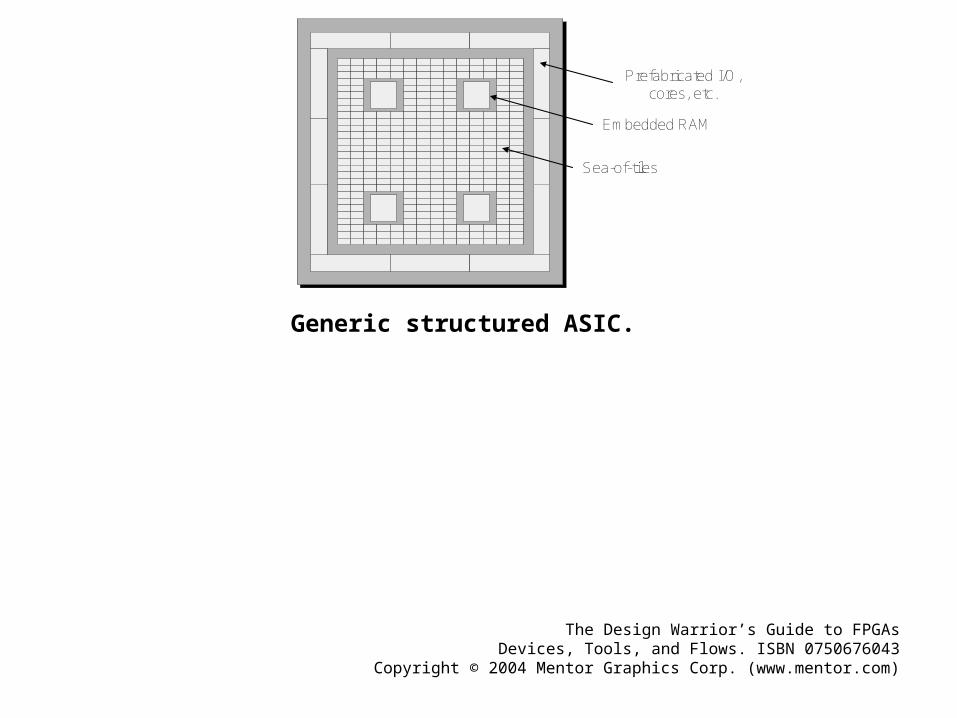
Prefabricated I/O,cores, etc.
Embedded RAM
Sea-of-tiles
Generic structured ASIC.
The Design Warrior’s Guide to FPGAsDevices, Tools, and Flows. ISBN 0750676043
Copyright © 2004 Mentor Graphics Corp. (www.mentor.com)
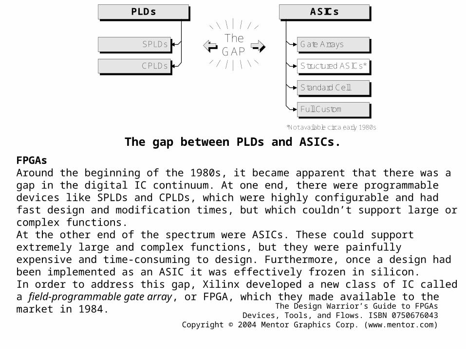
PLDs ASICs
Standard Cell
Full Custom
Gate Arrays
Structured ASICs*
SPLDs
CPLDs
*Not available circa early 1980s
TheGAP
The gap between PLDs and ASICs.
FPGAsAround the beginning of the 1980s, it became apparent that there was a gap in the digital IC continuum. At one end, there were programmable devices like SPLDs and CPLDs, which were highly configurable and had fast design and modification times, but which couldn’t support large or complex functions.At the other end of the spectrum were ASICs. These could support extremely large and complex functions, but they were painfully expensive and time-consuming to design. Furthermore, once a design had been implemented as an ASIC it was effectively frozen in silicon.In order to address this gap, Xilinx developed a new class of IC called a field-programmable gate array, or FPGA, which they made available to the market in 1984.

The Design Warrior’s Guide to FPGAsDevices, Tools, and Flows. ISBN 0750676043
Copyright © 2004 Mentor Graphics Corp. (www.mentor.com)
The first FPGAs were based on CMOS and used SRAM cells for configuration purposes. Although these early devices were comparatively simple and contained relatively few gates by today’s standards, many aspects of their underlying architecture are still employed to this day.The early devices were based on the concept of a programmable logic block, which comprised a 3-input lookup table (LUT), a register that could act as a flip-flop or a latch, and a multiplexer, along with a few other elements.
3-inputLUT
abc
flip-flop
clock
muxy
qd
The key elements forming a simple programmable logic block.

The Design Warrior’s Guide to FPGAsDevices, Tools, and Flows. ISBN 0750676043
Copyright © 2004 Mentor Graphics Corp. (www.mentor.com)
|
&ab
cy
y = (a & b) | !c
Required function Truth table
1011101
0000010100111001011101111
y
a b c y
00001111
00110011
01010101
10111011
SRAM cells
Programmed LUT
8:1
Mul
tiple
xer
a b cConfiguring a LUT.
The multiplexer feeding the flip-flop could be configured to accept the output from the LUT or aseparate input to the logic block, and the LUT could be configured to represent any 3-input logical function.Assume that a LUT was required to perform the functiony = (a & b) | !cThis could be achieved by loading the LUT with the appropriate output values.The 8:1-multiplexer-based LUT is used for purposes of simplicity.
The Design Warrior’s Guide to FPGAsDevices, Tools, and Flows. ISBN 0750676043
Copyright © 2004 Mentor Graphics Corp. (www.mentor.com)
Programmableinterconnect
Programmablelogic blocks
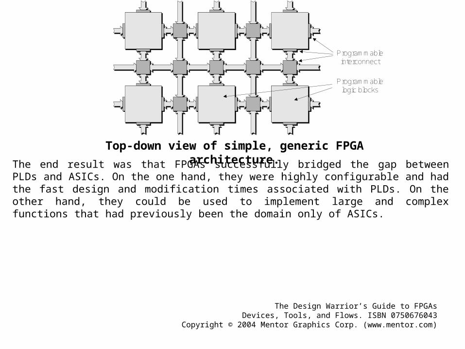
Top-down view of simple, generic FPGA architecture.
The end result was that FPGAs successfully bridged the gap between PLDs and ASICs. On the one hand, they were highly configurable and had the fast design and modification times associated with PLDs. On the other hand, they could be used to implement large and complex functions that had previously been the domain only of ASICs.
The Design Warrior’s Guide to FPGAsDevices, Tools, and Flows. ISBN 0750676043
Copyright © 2004 Mentor Graphics Corp. (www.mentor.com)
ASIC
FPGA
To other chipson the board
To other chipson the board
To other chipson the board
To other chipson the board
Platform FPGAsThe concept of a reference design or platform design has long been used at the circuit board level. This refers to creating a base design configuration from which multiple products can bederived.
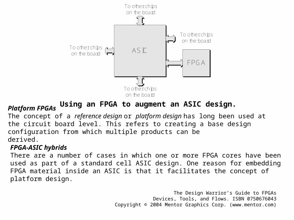
Using an FPGA to augment an ASIC design.
FPGA-ASIC hybridsThere are a number of cases in which one or more FPGA cores have been used as part of a standard cell ASIC design. One reason for embedding FPGA material inside an ASIC is that it facilitates the concept of platform design.