Embed Size (px)
Citation preview

The design of a multiplying digital-to-analogconverter for wideband hybrid computation
Item Type text; Thesis-Reproduction (electronic)
Authors Eddington, Don Charles, 1945-
Publisher The University of Arizona.
Rights Copyright © is held by the author. Digital access to this materialis made possible by the University Libraries, University of Arizona.Further transmission, reproduction or presentation (such aspublic display or performance) of protected items is prohibitedexcept with permission of the author.
Download date 28/05/2018 05:05:12
Link to Item http://hdl.handle.net/10150/347695

THE DESIGN OF A MULTIPLYING DIGITAL-TO-MALOG CON'FERT.ER FOR WIDEBAND HYBRID COMPUTATION
byDon. Charles. Eddlngton
A Thesis'Submitted to the Faculty of theDEPARTMENT OF ELECTRICAL ENGINEERING
In Partial Fulfillment of the Requirements For the Degree ofMASTER OF SCIBICE
In the Graduate CollegeTHE UNIVERSITY OF ARIZONA'
1969

STAT2M3NT BY AUTHOR
This thesis has been submitted in partial fulfillment of requirements for an advanced degree at The University of Arizona and is deposited in the University Library to be made available to borrowers under rules of the Library.
without special permission, provided that accurate acknowledgement of source is made. Requests for permission for extended quotation from or reproduction of this manuscript in whole or in part may be granted by the head of the major department or the Dean of the Graduate College when in his Judgment the proposed use of the material is in the interests of scholarship. In all other instances, however, permission must be obtained from the author.
This thesis has been approved on the date shown belows
Brief quotations from this thesis are allowable
SIGNED:
APPROVAL BY THESIS DIRECTOR
QgTA. KORN Professor of Electrical Engineering5 M / 1 1Date/

./iGMOV/LEDGEMENTS
The project described in this report was part of a continuing study of hybrid analog-digital computer techniques- directed by Professor G-ranino A* Korn at The University. of Arizona. The author wishes to acknowledge the suggestions„ encouragement, and guidance rendered by Professor Korn during the preparation of this thesis. He is .also grateful to the National Aeronautics and Space Administration and to the NASA Arnes Research Center for their support of the project under NASA Grant NsG 646,
iii

TLABLS OF CONTENTS
PageLIST .OF ILLUSTRATIONS e. ». . ......... » , . . .. e. » . , vLIoT . Oi- T ABLiijO @ 6 p. e- 6 o P o p p c o o c p o o c c e VI ■ABSTRACT p.p. e ©..p 6- ‘ p p © p e e e o 6 e e 6 o p * 6 o "VlXINTRODUCTION; * * , © * , , , © , © , , * * , , © , * * 1THE DECODER NETWORK «. . » . . « © » e o © e 0 © 0 » o e ~ 6THE DESIGN OF ?>©AC SWITCHES • 17
MDAO Switch Configuration Selection © © . e © © 17JFET Versus MOSFET Switches . . . . . . . . . . 22The.JFET Switch © . © . © © © © © © © © © © . © « 24
Oi* F . is uU t e © " © © © © ■ © © © © © © © 0 6 6 6 © 2 7Oi'4 OOcite © © © © © © © © © © 6 © o © © © e 28
' The MOSFET Switch . . . . . . . . . . . . . . . . 31ERROR AN ALYo 1,3 © © © © © p . © © © © © © © © ©© © . © 34
Errors, Caused "by Input Voltage Variation © © © 35Leakage-Current Error © © © « © © © © © © © © © 39Errors Caused by Temperature Drift of
Network Impedances © © © . . © © , © © © © 40High-Frequency Errors and Equalization © © © © 44Errors Caused by Switching Spikes » © © © © © © 45
CONSTRUCTION, TESTING, AND RESULTS © © © © © ' . © © . © 47Calibrauion © © e © © © © © © . © © © © © © © © 48Digital Switching Characteristics © . © © . © . 51Dynamic Characteristics © « , . © © © © © © © © 51
REFERjiN v o © © © © © ©■ © © © 6 ©© ©6 © © © © © © * © 80
iv

,ge
815
20
2130335050505253
57585959
. LIST OF ILLUSTRATIONS
Figure ,lc (a) Ladder Network MDAC (b) Weighted
Resistor Network MDAO e c « e e «, e2«, 12“Blt MDAO Circuit Configuration3e (a) Bipolar Transistor Shunt Switch
(b) FET Shunt Switch (c) FET Series Switch (d) FET Series-Shunt Switch
4c (a) Simplified FET Model In the ON State(b) Simplified FET Model in the OFF State .
5* JFET 'Switch Circuit Schematic Diagram » , *6c MOSFST Switch Circuit Schematic Diagram e ,7b Fully Assembled MDAC .86 MDAC Terminals On LOCUST Analog Patchbay 0 e9ft Circuit For Measuring MDAC Dynamic Error „ .10« Digital Switching Characteristics , «lie MDAC Switching Spikes12c (a) MDAC.Dynamic Error With Frequency .
Equalization and (b) Dynamic Error Without Frequency Equalization
13o MDAC Small-signal Frequency Response14» MDAC Operation at Computer Speed = .15o MDAC Resolution Near Digital Zero » , » » e
v

LI3T. OF TABLES
Table PageI . 12-Bit' MDAG .Specifications 0 e « o = e » » » e 5
XI MDAO Decoder Network Resistor Values = , » .• . •* 16III. ■ Output. Error..Caused. By Impedance Error In
Any. Given Component * ....... 36
vi

■ABSTRACT
This paper discusses the design and testing of a. high-speed, 12-bit multiplying digital-to-analog converter developed for use in wideband hybrid computerse. The circuit features ease of construction with.minimum component hand- selection, even though low network impedance levels are used in order to obtain accuracy at high analog computing frequencies. Zero-voltage-offset series field-effect transistor switching is utilized, and trimmer- adjustment of binary weighting in the resistor network allows calibration of the fully-assembled device while it is in the computer under normal operating conditions. The multiplying digital- to-analog converter ■'is capable of multiplying an analog signal-., by a digital number with a static accuracy of 0,025 ■ per cent, of half scale and a dynamic accuracy of 0,1 per cent of half scale at a.computing frequency of 10 Khz,
vii

INTRODUCTION
The objective of this thesis project ■was to develop a 12-bit multiplying digital--to-analog converter (HD AC) for ^he University of Arizona’s LOCUST/PDP-9 hybrid computer. With ordinary hybrid computers, the design of a 12-bit two1 s complement, digltal-to-analog converter. (DAC), and even the more difficult design of a MDAC, is a straightforward proposition; but in our case, the MDAC design proved to be one of the most difficult tasks.of the entire LOCUST project. -
The difficulty in LOCUST MDAC design is due to the exceptional bandwidth requirements of the LOCUST computer, which is capable of 2000 differential-equation-solving runs per second and which must handle analog signal voltages all the way up to 100 Khz,® For this reason, LOCUST operational amplifier summing resistance values are IK ohms to 10K ohms. The LOCUST MDAC (see Table I for complete specifications) is to multiply a 10 Khz sinusoidal Input by a digital word with a phaseshift error within 0.1 per cent of half scale, and its DAC network resistances must therefore also be between 2K and 10K ohms,- As resistance - levels are. lowered, electronic switch resistance variations and offset voltages become quite critical. A second serious-difficulty is that
1

2the wideband ■ amplifiers used in the LOCUST (30 Mhz at unity.' gain) faithfully transmit fast MDAC switching spikes uhioh would never be seen in conventional analog computers. Fortunately, in most applications (optimization, random-process studies), the MDAC1s usually switch only during computer RESET periods ©
The reason for the requirement of 12 bits (11 bits plus sign) is not really 12 bit accuracy (LOCUST has - an ac-
. . curacy within only 0,1 per cent of half scale for linear computing elements) but rather is 12-bit resolution. This - is needed' to keep sensitive system parameters being o'pti-
' mized from "hunting" excessively about their optimal value. In unstable systems, such as in trajectory optimization, a very small parameter change can produce a substantial .so.lu-
• tion change.The MDAC accepts the 12 most significant bits from
the PDE-9 accumulator- on an output command through a double- ' buffered interface (Wilkins 1969)© Its output voltage on
the analog computer patchbay is the voltageX X t■ A 0 - XA X-, (2.)"1*.. . . e X31(2)'’11-X0 (2)0 '2 1 1 ' V “
- where XA is a time-varying analog voltage between -kLO volts and -10 volts and Xjj is the binary number Xq . ... .Xjp from the 12 most significant bits of the PDP-9 accumulator.
■Important design objectives of this new MDAC are simplicity of construction, minimum calibration effort, and

reasonable cost. Construction of only a few units rather than .a large number also enters into consideration».
. 3he .University of - Arizona8 s earlier ASTRAC I.I/PDP-9 -hybrid computer utilizes transistor shunt switches , in the MDAC's® The switches must.be individually compensated to minimize, output error due to the offset voltages of the saturated transistors by a tedious.process of resistor hand selection? The use of field-offect transistors (PET1s) with .zero off set,'Vo,itages suggests itself as a remedy for 'this problem«
Most present MDAC's are'designed with.fixed preclusion resistors in the decoder networks. If the Impedance levels of the MDAC are low, these resistors must be either very high-precision units or else must be hand selected«Very accurate resistors are .expensive; and hand selection, which is time consuming and requires large stocks of resistors , is not too desirable when- only a few units are being built for a, particular system? \
While transistor shunt switches require hand compensation for offset, series PET ■ switches require either hand, selection or resistor padding to account for the PET resistance?. This is especially important in view of the low impedance -levels used in LOCUST. '
The MDAC described in this report uses PET switches for zero offset, a, binary weighted resistor decoder network

4to minimize the number of expensive snitch components9 and discrete component level converters and snitch drivers for minimum cost. Trimmer adjustment of network resistances compensates' for both snitch, resistances and resistor tolerance errors In one simple' adjustment. No resistors hith tolerances of less than 1 per. cent are, required, and only one resistor must be hand selected for the entire MPAO. •Furthermore9 calibration can be made on the fully assembled unit.after it is in the computer' under actual operating ' conditions. Because construction and calibration time is 'minimized, the design is well suited for use when -a small number of high-speed, precision MDAC’s are needed at a reasonable cost o

Table I . 12-Bit MDAG Specifications
.Analog Input' voltage-Digital logic input levels;
ON state OFF .stateStatic accuracy ($ of half scale)Dynamic, accuracy of half scale)Switching .speed S
delay rise timesettling time (within 0,,025/S)
Output error temperature driftsworst case typical (measured)
Worst“Case switching spikes
Power supply requirements Power supply regulation Worst-case power.supply drain
Maximum MDAO power dissipation Current drain from digital logic
Analog input Impedance
-10 volts
0 volts -3 volts
0.025^11/5 LSB0.1/ at 10 Khz
40 nsec1.5 jusea
5 psec
±0.133 LSB/oe +0.02 LSB/oC±2.8 volts
(no output amplifier overloads are caused by worst-case switching spikes)
±15 volts±1/
34.2 mA from 4-15 volts78.5 mA from -15 volts
1.71 watts4.1 mA at 0 volts 0 mA at -3 volts
2K ohms

THE DECODER NETWORK
A multiplying digital-to analog converter consists of. a decoding network which converts the analog voltage into weighted currents.proportional to the digital number and an operational amplifier with low output impedance. The two types of decoding networks most commonly found are the mejghted-resi stor network and the ladder network o'
A ladder network (Pig* la) employs only two values 'of precision resistors. The analog currents flowing in the bits of a ladder network MDAC have been shown (Pearman and Popodl 1964) to be more evenly distributed through all bits than.the analog bit currents flowing in an equivalent weighted~resistor network MDAC. Because analog current (and:therefore power dissipation) is more equally distributed throughout the: bitp, and because resistance values are used which vary only by a factor of 2, the binary relationship of the ladder network bits should be easier to maintain with varying analog signal and environmental conditions *
The ladder network suffers from the disadvantage that wiring capacitances greatly increase from the most significant bit to the least significant bit due to the increasing number of resistor,junction points (with their associated junction-to-ground capacitances) in the analog
6 •

7signal current path as one moves toward the least significant bit« A second disadvantage is that it requires a single^pole double-throw switch, at the analog.input of each bit. If FET switches are used, two of the relatively expensive FET's are necessary in each switch. More complex ' driving circuits are also required..
A weighted-resistor network (Fig. lb) requires only a single-pole single-throw switch, or one FET per switch«Even if a single-pole double-throw switch is used in a serles-shunt'configuration (Fig. 3d) in a weighted resistor network, still only one of the transistors in each switch must be a FET. Because the FET and its associated level- shift and drive circuits are the most expensive part of each bit, one would like to minimize the number of FET‘s and switch components. In addition, because the impedance of each bit of a weighted-resistor. network is connected directly to the amplifier summing junction, wiring capacitances in the less significant bits should be smaller than those of a ladder network. For the above reasons, and because limited space in MDAG packaging for LOCUST required use of a minimum number of components, the weighted resistor type decoder was used rather than the ladder network.
A n-bit weighted resistor decoder consists of n binary related resistors R, 2R, AR, 2^R as in Fig. lb.Rote that the' switch resistance Rg must be included in each

8R.
I iI
I oRs 2R-R^----- W V -
2R
(a)
R-Rs R§ R
i
2nR-Rs Rs—AAAr— --- / -
(b)
Fig0 10 (a) Ladder Network MDAG (b) WeightedResistor Network MDAC

"bit. If the amplifier gain is sufficiently high, the summing junction is virtually at ground potential because of the negative feedback across the amplifier. The bit currents flowing .into the summing junction are therefore binary weighted, with X^/R in the most significant bit and -X^/ in the least significant bit©
The weighted resistors are switched in or out of the network depending on whether.a digital 1 or 0 is present at the switch drive of each bit© A digital 2’s complement number X-q-Xq ... © ©X^ then yields an analog voltage xou- s-* the amplifier output, where
• • • -*Xn (2)-n-X0 (2)0]The impedance level of the MDAG is given by the im
pedance of the feedback resistor. Because of distributed. capacitance effects associated with large resistances, the impedance level must be kept as low as possible .for good high frequency response. On the other hand, the switch error analysis presented later in this paper indicates that 10K ohms seems to be a minimum value for the impedance level if switch errors are to remain within limits over normal operating temperature ranges. Therefore the feedback resistor and first bit resistor are chosen to be 10K. Bit resistors then double for each bit until an impedance of 20.4811 ohms is reached in bit 11. Since the 2^^ : 1 resistance ratio is not practical, T-networks are used for the

■ 10 low-current branches« The non-zero switch resistance R must again- be included in transfer impedance calculations for T~networks» Impedance in the T-netvrorks must also be kept: fairly low because of distributed capacitances„ For good frequency response in the high-impedance bits, resistances used in T-networks were- limited to a maximum of 40.2K ohms,
Other considerations in the selection of resistances for the decoder network include the feedback ratio of the output amplifier, which determines its frequency response, and the current load on the driving analog amplifier. Because phase-shlft error of an operational amplifier varies approximately inversely with the feedback ratio (Korn and Korn 1964), the summing-junction-to-ground impedance must be as high as possible. Because the preceding analog stage has drive capability limitations, the input-to-ground impedance must also be high enough to keep drive requirements within these limits. Worst-case conditions for feedback ratio occur when all switches are in the .ON state- (logical l-)„ Because a shunt transistor will be used in each bit (for reasons explained later), the MDAC input impedance is independent, of the switch . settings. . ,
If the switch'resistance were a constant Rg for all switches, this fixed value could be considered when

11selecting decoder1 network resistance» Unfortunatelythe ON resistance of present field-effect transistors can vary quite a hit from device to device. A TIS41 JFET, for instance ,- can have a selection resistance of anywhere from 15 ohms to 25 ohms; and the SS2012 M0SFE1 can have a selection resistance of from about 150 ohms to 250 ohms. In addition, unless very high precision resistors are used, the tolerances of the resistors in. each bit can add up to an impedance variation which is larger than the allowed tolerance for the transfer impedance. Such variations in switch resistance and resistor values would normally have to be compensated by hand selecting or padding resistorse This is a tedious process, which is best implemented in large production quantities.
-A simple method of adjusting the transfer impedance of each bit to compensate for both the switch resistance and the resistor tolerances in one step is to add a trimmer potentiometer to the resistor network of each bit.. If the network is designed so that small variations in the trimmer have negligible effect on the transfer impedance, an inexpensive carbon-film trimmer can be used in all except the first few most significant bits. Series wire-wound trimmers are used in the first 3 bits, with maximum, resistances, kept small (less than 2*5% of the total bit resistance) in order to. minimize the effect of

trimmer capacitances and inductances. The transfer impedance for each bit is designed so that a full OFF (zero ohms) to full ON (maximum'resistance) excursion of the trimmer causes only enough variation in transfer impedance to compensate for worst-case switch resistance and resistor toleranceso If this is done, the effect of the temperature coefficient of the carbon trimmers is reduced so that the output error introduced by trimmer temperature coefficients is acceptable.. This statement will be justified in the error analysis later in this report= •
Adjustment of each bit and of the feedback resistor, by a procedure described in a later section,, eliminates static tolerance errors. Leakage currents and voltage and temperature variations then remain as the only sources of static error in MDAC resolution and monotonicity»
Worstscase design equations may be used to determine values of standard resistances which assure worst- case tolerance and switch resistance compensation for a full OFF to full ON trimmer variation» Assuming the circuit configuration and terminology of Fig. 2, the resistor values for the n bit transfer impedance must satisfy the following worst-case relations:
For bits 0-2:Rpn(max)™ 2 10Iv ^ )~Rln( ^™^sn(min) R-,- 1 |2n (10Kn) (1-6)~R , J

13For bits 3-11:
.R2n:(1"4) tRsn(min)
f (lOK^) ( ) -Rsn(mln)- ) (1-5 )
R^Cl-S)
» m - +V (1-4)rtV(ma*)R2n(14-S)4-Rsn(inax^
\f (lOKn) (1- S )-Rsnimax)- ) (I d )]
where the subscripts:max and mln respectively indicate maximum or minimum worst-case values, and where 6 is the precision resistor tolerance, Rgn is the FET ON resistance of the n^-bit switch, and Rpn is the n^-bit trimmer resistance, Calculations for bits 3 through 11 were made •assuming 1% tolerances. To minimize potentiometer resistance in bits 0 through 2, fixed resistor tolerances of 0,5% were assumed in the calculations for these bits,
The calculated resistor values for the transfer impedances of the 12 bits, corresponding to the terminology of Fig. 2, are shown in Table II. The type of switch used in each bit is indicated under Rsn» All fixed resistors are 1%. . 20K trimmers are used in the design simply because of

14availability of a large stock of this value in our laboratory o Since errors in the least significant bits have little effect on the output, the trimmers in the last few bits could, be omitted when designing the MDAC«
The: minimum, possible output amplifier feedback ratio of the MDAO with all switches in the ON state is o201s and it is 1.0 with all switches OFF. Worst-case load impedance to the preceding analog stage is 2K ohms (-5 ma at -10 volts)0

15
sn |
Pig. 2, 12-Bit MDAC Circuit Configuration

I
Table II MDAG Decoder Network Resistor Values (Resistor notation corresponds to Figs 2)
no s (n) % n Rpn ^ln Rxn•wseaSamSs 5 m0 TIS41 200 9*86%.1 TIS41 500 19*76% «3 «=»2 TIS41 IK. 39*5% «,c*.3 TIS41 20 K 10% 30,1% 10% 23*7%4 . TI:S4l 2 OK 10% 40,2% 4.42% 16.9%5 SS2012 20K 40 s 2% 40,2% 8,66% 25*5%6 SS2012 20K 40„2K 40,2% 3*57%. 12,1%7 3S2012 20IC 40,2% ' 40.2% 1.58% 7.15%8 532012 20K 40,2% 40.2% 750 3*74%9 ' 332012 20 K 40,2% 40,2% 348 010 532012 20K '40,2% 40*2% 178 011 332012 20K 40,2% 40,2% 82,5 ' 0
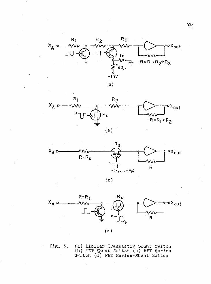
THE DESIGN OF MDAC SWITCHES
M'DAC Svritgh Qonfxkura11 on Selection -Bipolar transistor shunt switches, such as the one
shown in Fig. 3a$ create MDAC output errors due to the offset voltage and collector resistance. In a low impedance MDAC, these errors must be compensated "by individual trial- and-err or selection of an offset resistor for each switch in the device (08Grady 1969). Field-effect transistors have the advantage of zero offset voltage, hut higher drive voltage are required. In addition, the ON switch resistance of most FET$ s is higher than that of a bipolar transistor. A FET used as ah analog switch may be represented simply by a variable resistance as shown in Fig. 4, with a, low resistance in the ON state, and an extremely high resistance in the OFF state. When a FET is used as a shunt switch as in Fig, 3b, ' output voltage [error appears in the OFF state due to the non-zero FET resistance. This is also undesirable.
If a FET is used in a. series switch configuration (Fig. 3c), no offset voltage problems exist in either state; and no hand-selected offset compensation is necessary. The FET appears as a pure resistance in the ON state and a. nearly Ideal open circuit in the OFF state.
17 '
18Series switches have the advantage that the feed
back ratio @ .of the output amplifier always remains higher than for-an equivalent shunt switch. For the single-bit shunt switches of Figs-. 3a and 3b, p is -g- in the Oh -state and always less than in the OFF state. For. the series switches, of Figs. 3c. and 3d, the feedback ratio is with the.switch ON and 1 with the switch OFF. Since, as a first approximation,: operational amplifier phase shift varies inversely with ^ (Korn and Korn 1964), the high-frequency error should be lower for a series-switched MDAO than for a shunt-switched MDAC of the same impedance level. Again, the input impedance seen by the preceding state is always higher in the OFF state for the series-switched bit than for the shunt-switched bit, requiring less analog current ,drive and less power dissipation in the precision resistors© For the above reasons, a series switch should be preferable to a shunt switch©
Most junction FET's with low ON resistance have the disadvantage that they require substantial gate-voltage swings at the gate to turn the FET off. For reasons explained later, * this high gate. OFF voltage requires that a bipolar, shunt transistor be used to ground the source of the FET when it is turned OFF. The resulting series-shunt current switch is. shown in Fig. 3d. -
The -series-shunt current switch has all the advantages' of the series switch; and, since the shunt

19transistor is only grounded when the FET.is open, the feedback ratio Is unaffected. . No offset error due to the shunt-}transistor can appear in the OFF state because the. FET is open-circuited. In addition, the shunt transistor provides a path for the analog signal current to flow to ground when the FET is OFF, If the switch Is at the summing junction o f the amplifier, this results in a constant impedance to the preceding analog driving stage regardless' of the state of the switch. Currents in the precision'resistors are constant regardless of the state of the switch, causing uniform power dissipation and thereby reducing the possibility of binary errors due to thermal variations in the resistors, Also, since the shunting transistor is driven by a signal complementary to the FET drive signal, the switching spikes of the two devices tend to cancel partially.
For the above reasons, the FET series-shunt current switch-was chosen as. the. optimum configuration for switching the MDAC, In addition to the advantage of constant input impedance,. placing the switch at the summing junction rather than elsewhere in the bit impedance has the advantage of lower FET gate-drive and transistor.base-drive level requirements, better high-frequency switching, and better isolation of the gate drive from the analog signal.
20
(a)
oX
R = Ri + R(b)
Fig. 3» (a) Bipolar Transistor Shunt Switch(b) PET Shunt Switch (c) PET Series Switch (d) PET Series-Shunt Switch

21
Pig,;. 4
Rds
g s s
(a)
RoffO D
d g of f
( b )
>) Simplified FET Model in the ON State 'b) Simplified FET Model in the OFF State

Ii
22
JFET Versus MOSFET Switches Although voltage-offset problems do not exist in
PET switches, error results from the variation of. drain-to** source ON resistance (R&s) with temperature, with drain current (Ig), and with gate-to-source voltage (VgQ)« These variations are different for junction field-effect transistors (JFET‘s) and for metal-oxide-semi c onductor FET's (MOSFET8s) »•
Most inexpensive MOS field-effect transistors have relatively high drain-to-source ON resistances compared to that obtainable in junction field-effect devices« For this reason, the variation in R^s with drain current is larger for MOSFET1s» The variation of g for the 25 ohm.JFET used will be shown to be only a fraction of an ohm over the -1 m&/range of the analog current in the most significant bit, while similar current variation in the 250 ohm MOSFET would cause a resistance variation of several ohmso
N-channel junction FET8 s have the advantage that they are in the.ON state when the gate-source voltage is zero. Since the summing junction of the operational amplifier is a virtual ground, the gate need only be grounded in order to insure that the gate voltage will follow the source voltage and will thus minimize variation of R^g*The ON resistance of a JFET is therefore independent of power supply drift and regulation. The MOSFETVs, however,

must "be biased at some positive value of gate voltage to be in the ON state* ■ Any change .in this positive gate bias due ..to..power ■ supply drift or power supply regulation leads to additional variation in R^s for the MOSPST*.
While the temperature coefficient of ON resistance is lower for MOS transistors than for JPET's, the fact that the overall drain-source resistance of the JFET is much lower still leads to a smaller variation of R^g with temperature than for. the. MOSFET'.
From the above comparison} it is obvious that the JFET would make a much more accurate series switch than would the MOSFET. Low resistance JFET1s5 on the other hand, are more expensive than MOSFET*sj and low JFET ON resistance necessitates a large junction with associated high junction capacitance (Fig. A)a As a comparison* the TI341 JFET has a gate-to-drain capacitance in the OFF state of more than 8 picofarads, while the 332012 MOSFET has a maximum, gate-to-drain capacitance of only 1 picofarad. Because the JFET capacitance is caused by a reverse-biased p-n junction, the capacitance increases still further when the switch is in the ON state. The high capacitance between the gate and drain causes a large surge of injected current into or out of the summing junction of the operational amplifier vjhen the gate drive is switched between its two states. The current surge creates output voltage switching

24spikese Ordinarily, slow operational amplifiers could not follow such short9 high-magnitude- output spikes. The use of 30 Mbs amplifiers in the L00U3T system, however, causes these spikes to be a major problem. The switching spikes can be partially cancelled by feeding an inverted .spike to the summing junction, but complete cancellation is not possible.
A tradeoff between accuracy and switching spikes indicates the .use of M03FET switches in the least significant bits.for minimum switching spikes, with JF3T switches in the most significant bits for static accuracy. An examination of the error variations for the two switches indicates that the current and temperature variations of R^g , in MOSFSf switches can be tolerated in bit 5 and lower, while their use in bit 4 and higher would increase the output error significantly.
The JFST Switch The MDAC switches were designed to operate'from
the 0 and -3 volt logic levels of the PDP-9/L00U3T interface.- Each MDAC bit is,OFF (passes no analog signal) when the interface output flip-flop corresponding to that bit is zero volts, and ON when the flip-flop output is below -3 volts.. - • -
An-channel junction field-effect transistor has lower Oii resistance ,than a p-channel device of comparable
25geometry $ and. therefore; n-ohannel PET*s are. usually used " when low resistance with minimum.capacitance is desired.The TI8-41 symmetrical n-channel JF3T has :a source-drain ON resistance of less than 25 ohms when the gate-source volt- age VgS .is zero. As VgS is made more negative? the resistance increases to an OFF resistance of several hundred megohms at Vgg" ^10 volts» Thus the 0 and -3 volt logic levels must "be converted to at least -10 volts and 0 volts at the gate to drive the FET into the appropriate states» .Because large, logic signal swings are required to drive the JFETj standard low-level integrated-circuit logic circuits cannot be used as drivers. Integrated-circuit FET drivers capable of these large level swings are presently quite expensive. To keep HDAC cost at a minimum, discrete component drivers were therefore used.
Without a shunt transistor in the most significant bits (Pig. 3c), the voltage at the source of the JFET would follow the analog input voltage when the FET was in the OFF state = Since the gate must always be held at least 10 volts negative with respect to.the source and drain, an analog input of -10 volts would mean that the gate OFF drive voltage would have to be more negative than -20.volts.. Because the negative power supply voltage in the analog computer is only -15 volts, the source of the FET must be grounded when the FET is turned off. For this reason, shunt transistors

26■are provided in the moat-signlflcant-bit JFE5 switches (if JFET's were used in lower bits, where the T-networks reduce the analog swing at the source to below —5 volts when the switch if off, the shunting transistor would not be necessary)*. "
The use of a shunt transistor has other useful advantages in addition to insuring sufficient OFF gate voltage A common problem in JFET series voltage switches is that at high analog signal frequencies' the gate-source and gate-dratn capacitances (Fig. 4) provide, a path for the analog signal to pass into the amplifier.summing junction even when the. FET is turned off» Grounding the FET sources. eliminates the possibility of capacitive feedthrough from the -10 volt analog voltage swing at the source when the switch is OFF*
An additional advantage of the shunt transistor is the possibility of partial compensation of the FET switching spikes* If a NPN transistor is used as the shunt transistor, the polarity of its base drive voltage causes switching spikes complementary to those of the FET*
Because the switching spikes due to the JFET and to other capacitances in the circuit are much larger than the complementary spikes of the KPN. transistor, some additional spike compensation must be included. If no additional com-1- pensation were used, switching spikes on-the order of 3 to ■

274 volts for each JFET switch and 1 volt for each M03FETswitch could be possible.. These spikes would add, so that ,actual overloading of the output amplifier would be possible for worst-case switching.
Switching-spike .compensation is accomplished by feeding inverted spikes to the summing junction of the operational amplifier through a differentiating capabitor from the first gate drive stage. The inverter stage delay is short compared to the duration of the switching spikes, so that'the major portion of the spikes can be effectively . cancelled by selection of an appropriate value for this compensating capacitor.
The circuit of the complete JFET switch is shown in Fig, 5. One inverter provides the drive for the shunt transistor, and two stages provide the 0 and -10 volt gate drive for the FET. Operation of the switch in the OFF andON states is described below.
OFF StateWith the logic input at ground, the analog signal
current is.routed to ground rather than to the summing junction. Transistors and are saturated, providing approximately -13 volts at the gate of the JFET. to turn it OFF. Diode Dy is reverse biased, and'diodes Dr and are conducting. Diodes Dg,. and supply" 4-0.7 volts

28to the base of Qg *o hold It in the saturated state; and Rg provides the necessary base and diode current® is a germanium diode, while Dg and are silicon<>
ON State./ With'the logic input at -3 volts, the analog signal
current is routed to the summing junction, and the shunting switch is opene- To turn the FET ON, diode is placed inseries with the gate, and the collector of is then driven to any voltage greater than zero = The low leakage diode
becomes back biased, and the gate voltage remains at zero voltso The addition of by itself would cause turnon switching time to be greatly increased because the gate would have to charge entirely through the gate-source and gate-drain capacitances during turn on® To correct this problem, Ry must be added as a low-impedance path from the gate to ground® Ry is chosen experimentally to give the . desired turn-on time®
' In the ON state, transistors Q-, and are OFF®The collector voltage of Q- is -f-0®7 volt, and the gate voltage of Qij is 0 volts® Rg can be very large, since its only purpose is to provide current to hold Dy slightly forward biased when the FET is on* Resistor R^ acts as a, pull down resistor to turn Qg off ? and diode Di\ clamps the Qg base vpltage at -0*7 volt to protect the base®
The values of R^ through Rg are calculated using

29worst-oase design equations, assuming resistor.tolerances of 15$ and power supply tolerance of l$e , Worst-case logic inputs are assumed to be .-0.3 volts and ~3«2 volts. Capac* ito^ is a speed-up capacitor selected experimentally«Cg is the FET switching spike compensation capacitor .which is also determined experimentally® Because saturated transistor switching is used, the -15 volt power supply leads are filtered to isolate the MDAO.transients from the analog supply®
Impedance levels in the switch are chosen to give drive signal transition times of approximately 1 microsecond as a tradeoff between switching spikes and settling time® Note that extremely fast switching times are not desirable because ,of the larger switching spikes created by fast drive, signals In' FET*s® Slower drive signals are, of course,, not tolerable in view of the 250 Khz maximum-data output rate of the digital computer interface®
Power dissipation in the switch-driving circuits is an important consideration, since excess dissipation in the MDAO’ can lead to temperature drift. No current, is drawn at the driver-circuit inputs when the switch is ON (digital input at -3 volts), and approximately 3°5 mA is required when the switch Is OFF (digital input at ground)® Power supply drain in the ON state is only 1.05 mA from 415 volts and 2.18 mA from -15 volts, and drain in the OFF state is 1.1 mA from 415 volts and 4*5 mA from -15 volts®

30
analog current °' input
to Gdigi talinput
(0.-3V)
+ I5V
+ 15V
R2
-15 V
Q1=2N4125 Q29%=2M3904 Q4=TTS41 D, =11281 D2“D?=1N914 Ci =22 pP 02=7.5 pF
Ri=3.3K ohmsR2=22KR^,R7=10KRa=8:2K:Rn=l8KR5=68Kr8=iook
Fig. 5. JFET Switch Circuit Schematic Diagram

31The MOSFET Switch.
The MOSFET switch is similar to the JFET switch*The gate drive voltage, however, swings from +8 volts in the ON state to -6 volts in the OFF state*
The 882012 operates in both the depletion and enhancement modes * The maximum ON resistance is 250 ohms for a gate-to™source voltage of greater than +5 volts.* Measurements of versus V„CT for the 882012 in.the labor-Uo gSatory indicated that the rate of change of with Vp,sdecreases as Y _ is increased* For this reason, it isdesirable to operate the .MOSFET at a gate voltage largerthan 4-5 volts in the ON state* A more negative thangs-5 volts insures depletion of the channel and turns the device off.
The circuit schematic of the complete MOSFET switchis shown in Fig * 6* Modification of the JFET switch toaccomodate a MOSFET is accomplished by replacing Dg, Rg,and D7 with R„, R . , and R respectively* Rn is tied to
( 9- 10 . 11 * ■. v 11-15 volts rather than to ground* and R , are eliminated*
In the ON state, R ^ and R ^ form a voltage divider at the gate to set the 4-8 volt bias* In the OFF state, Qsaturates and thus parallels Rp with R-q to bring VgS to -6 volts *
The NPN shunt transistor is necessary in the MOSFET switch for a different reason from that for the JFET switch. The ON resistance of MOS devices increases

32as the square root of source-substrate voltage (Schmid1968) o To eliminate variations in R vjith-Vg^, the SS2012is constructed with the source shorted to the.substrate«While this.improves CM resistance behavior, it also createsa p-n junction between the source (substrate) and drain.Thus, when the MOSFET is turned OFF, the source voltagemust not be allowed to become more than about 200 mv, posi-
'tive with respect to the drain* It if does, the junction will become forward biased®
Worst-case design was again used to calculate resistor values, assuming the same worst-case parameters as for the JFET switch. Capacitors were chosen experimentally 6
Power supply drain of the MOSFET switch in the ON state is 1,95 mA from +15 volts and 3,25 mA from -15 voltsy and drain in the OFF state is. 4*1 mA from +15 volts and .8 mA from, -15 volts. Current required at the switch input - is zero when at -3 volts and 4,1 mA when at ground.

analog .current ^
inputto g'digital
input(0,-3V)
- 15V
%=:2N4125%=SS2012Di=lN28lDp»D3»D4=lN914cf=22 pF03=2.5 pF
H1=3o3K ohms Rp s R, 1 =22KRI=8t2KRc=l8KR?=68KRq=2„7KR109 «SK
Fig. 6. MOSFET Switch Circuit Schematic Diagram

ERROR : ANALYSIS
•Calibrating the MDAC while it is in the computer under actual operating conditions allows essentially complete- compensation of resistor tolerance and switch resis-- tance variations for a given set of environmental conditions and ■ for a given analog input voltage. For these particular conditions, because offset voltage error is zero, the . only remaining static error is due to leakage currents.A change in environmental conditions or variations in the analog input voltage can, however, cause errors« In addition, dynamic errors caused by the unavoidable capacitances in the MDAC' circuit become very significant as the analog signed frequency increases.
To insure 12-bit resolution, the worst-case static resolution error for any possible switch combination should be less than or equal to one-half the least significant bit (LSB)o- Worst-case errors in resolution occur near digital zero crossing, where all switches change state« For a 12- bit MDAC, the.total allowable non-monotonic, static binary , error is therefore LSB - 1 / ( 2 - 0,0244/ of half scale. Dynamic errors in the analog output voltage caused by capacitances in the system must bring the total error to less than 0.1/ at a computing frequency of 10 Khz to meet specifications of the LOCUST system,
34

35The effect of a variation or error in the impedance
of one. particular component of a . particular .bit- on overall output error can be found by differentiating the expression for MDAC output voltage with respect to the component in question„ Assuming the notation for each component that is shown in Pig.' 2, with T-networks in all but the 3 most significant bits, the output error caused by changes in the impedance of any given component may be expressed as per cent of half scale change in output voltage for a per cent change in the impedance of the. given component. The resulting expressions are summarized in Table III for each component . in the MDAC network. These relations will be used to relate the effect of various errors to overall output erroro
Errors Caused by Innut Voltage' Variation The channel resistance of both junction and MOS
type: field effect transistors varies as a function of drain current in the device. Time-varying values of current through the non-zero switch resistance cause the drain-.to- source voltage to vary. This in turn causes variations in gate-to-source voltage and channel resistance, since PET ON resistance is a -function of V„a»

36,Table- III; Output Error Caused By Impedance
. . Err or In Any'Given Component, (Component notation corresponds to Fig; 2)
Component (n'kk bit)
% 0RpoRS0RlnRpn.Rsn
erf/a error (of half scale) in MDAC output, voltage /i change in impedance of component
> n-O
> n-l92
RIn
R2a
Rsn> n=3-ll
P,•xn
R,yn
Rpn
+ 1+ (R10/10K.) l(Rpo/l°K)+ (R.s0/iOK)
-(2)-2n(R^/iOK) -(2)-2n-(R n/lOIC)lr*~-.(2)~2n(Rsn/lOK)
(2)-n. 1- ^ 2 ^ Rsn)2n (lOK)
-(2)
(2)
+ ( 2 )
t(2)
f(2)
-n RIn2 (10%)
R2n- R2nf'Rsn
-n
-2n
R1- ln
rf1 (10K)Rsn
R2nf"Rsn,
■2n
-2n
Rln R2n^Rsn . h ^ U o k)
RlnRTO(R2n^R3n).(Ryn+Rpn)2tl0K).-!
■ ' V ^ p n ’ 1010.

37The channel resistance of a junction FET biased
near zero gate-to-source voltage is given (Shipley 1964) by
H. d a " T T = v 7 y ...........
where is the value of channel resistance when Vgg=0and Vp is the pinchoff voltage of the JFETo Differentiation of this expression with respect to VgS shows that the per cent change in channel resistance for a small change in VgSis given by
* Ras . AVga% 7
Since the maximum R^g of the TIS41 is 25 ohms, the maximum variation in VgS in the n 02 bit for a -10 volt analog input is "fc (2)~n (25mV)» Assuming a minimum pinchoff voltage of 4 volts, the maximum per cent variation in switch resistance is -(2) n (0o625%) of total switch resistance, or -(2) n (Oe156) ohmse From the expressions in Table III,this results in a maximum output error of -0B00156^ of half scale for bit 0, ?0e00039% for bit 1, f0*0001% for bit 2, and less than 70*00004% total for bits 4 and 5»
, MOSFET channel resistance varies in a more complex manner than does JFET resistance (Schmid 1968)* Resistance of the 882012 varies less than 2%/mA of drain current for gate bias voltages greater than 6 volts*. The worst-case change in R^g for the n^-bi.t switch is,, therefore, given by (2) n (4%), or (10/2^) ohms * Output error is less than

38>0.00003,1$ of. half scale, because the MOSFET is used only in the low-order- bits® •
Assuming that all bit resistances are calibrated at one analog voltage extreme (+1.0'volts or -10. volts )„'the ■ worst-case output error occurs when the analog input X is at the opposite extreme. Bit 0 is driven by X, and all other bits are driven by -X. The error due to bit 0 is therefore twice as great, and the error due to all other bits-is zero. Maximum worst-case output error in the MDAC ..due to analog input variations is »00312$ of half scale.
In addition to input-current variation, the SS2012 • MOSFET OH resistance varies with the drive voltage VgS, and therefore with power-supply drift. Variation in R^g is less than•20$-per volt change in VgS for VgS 6 voltse Assuming power supply regulation of. 1$, worst-case. change in VgS is less than 100 mV, and hence R^s changes by less than 2$ (or 5 ohms). Total output error for bits 5 through 11 is less than .00074$ of half scale. Because the gate drives of the junction FET8 s used in the most significant bits are at ground when they are in the OH state, power- - supply variations have no effect on the switch resistance of - the first five bits. The large resistance variations. in the MOSFET switches, although they have little effect on. output • error when used in the- lower bits, are another significant reason why the MOSFET was not used for the most significant bits of the >1DAC..

The precision resistors employed in the MDAC decoder network; have a maximum voltage coefficient of 5 .ppm/volt,: V/orst-case output error occurs when bit 0 is at one analog voltage extreme, and all other bits are- at the other. Transfer impedances of the first 3 bits were constructed from two resistors per bit rather than one, and the maximum voltage across any precision resistor in the MDAC is thus -5 volts, Worst-c.ase output error, is., therefore, -0e005$ of half scale.
Total worst-c&se output error in the MDAC due to analog input variations and power-supply drift for both the switch resistances and the bit network resistors is 0,00886,f, or 0,182 L3B, ■
Leakage-Current Trror Output-voltage error due to leakage current is
equal; to the feedback resistance (10K ohms)..times the sum of all leakage currents. In the ON state, output error is caused by collector leakage in the shunt transistor and by gate leakage in the FET, In the OFF state, error is caused by F3T gate cutoff current, Because the collector-to- emitter voltage of the cutoff NFN transistor is never more than 25 mV, collector. leakage of the 2N3.904 was less than 40 picoamperea at 25°C in all'cases measured, Specified maximum gate leakage at 25°C is 0,2 nanoamperes for the JFET and 1 picoarnpere for the M03FFT. Leakage currents of

both the JFET and the shunt, transistor double with every ■ 10°O'- of temperature increase. Because the drain is grounded in 'the OFF state,. drain-to-sourc.e cutoff current of the. PET is negligible compared to gate cutoff current. Assuming a maximum operating temperature of 40°G, worst-case total output voltage, error due to leakage currents in all bits is less than. 50 pV,
Special care must be taken to remove all excess solder flux from printed-eircuit boards when constructing accurate analog circuits, such .as a MDAC. If excess flux is not properly removed, it can produce leakage current errors larger than those due to the transistor leakage currents,
. Errors Caused by Temperature Drift of Network Impedances
A significant error in the >!DAG is that caused by variations in switch resistances, potentiometer resistances, and precision resistor values as a function of temperature. Although precision resistors with small temperature coefficients.are used, the small variation can be quite significant. While switch and trimmer resistances have smaller absolute values, they have much larger temperature coefficients than the fixed resistors.• Fortunately, because most of the error is due to the first few bits, temperature error can be minimized by careful design of the channels for these bits.

41Because the effect ,on output error of the n^n~blt
switch resistance varies as (2)”^n » the error caused by. the switch in bit 0 exceeds the sum of the errors in .all other bit,s» To minimize output , error, therefore, the JPET in bit 0 is selected for an ON resistance'of less than 20 ohms.
Since temperature-drift effects in the switches ofbits 1 to 11 tend to partially cancel the drift of theswitch of bit 0 (which has an analog input of oppositepolarity), the worst-case output switch-drift error occurswhen only bit 0 is ON and has maximum drift,
.The. TI341 has a temperature coefficient of -i-0o65^/0Gto 0,7;£/°C» As a conservative estimate, the 3.32012 M0.3FET.is assumed, for purposes of worst-case analysis, to havea minimum temperature coefficient of O,lX/°0, Using therelations of Table III, the maximum output voltage drift(in per cent of half scale) due to bit 0 switch drift is*0,00l4i€/oC; and the minimum output drift due to bits 1through 11 is -0,000375/3/°C. The worst-case output driftis therefore 4-0,029 L33/°0, At digital zero crossing (when
< .all switches- change state), where temperature drift is most likely to effect hDAO monotonicity, worst-case drift is •5*0,0212 L33/0G, •
Over the temperature range under consideration, the .carbon- trimmers have a negative temperature coefficient of

-600 ppm/0C maximum; and the wirevzound trimmers have a negative coefficient.of -50 ppm/°0 maximum. The worst- case trimmer drift corresponding to worst-case F3T drift ■occurs when, bits 1 and 2 have maximum drift and all other trimmers are at zero. Output drift caused by the trimmers for this case is -t-0.000094//°0, bringing the total worst- • case output temperature drift due to trimmers and switches to *i-0..Qj51 LS3/0G and the total maximum drift- in resolution at digital zero crossing to +0.023 LS3/°C.
The. other extreme case exists when PET drift is • minimum in.bit.0 and maximum in all other bits, and when trimmer drift is zero in bits 1 and 2 and maximum in all other bits. For this case,' worst-case output drift due to all switches and trimmers is -0.029 L83/°C; but maximum drift in resolution at digital zero crossing is less than -0.01 LS3/°0. Most of the error for this case cones from trimmer drift rather than from FET resistance drift.
Worst-case output error due to the temperature coefficients.of the fixed, metal-film resistors occurs when bit zero has maximum variation in one direction, and all other bits have maximum variation in the opposite direction. For ±50 ppm/°C. resistors, this could cause an output voltage, drift error of ±0.0l//°G, or approximately l/5 L3.3/°G. This would mean that, even with zero switch error, 12-bit resolution could be guaranteed over less than a ±2.5°G temperature range.

43In actual fact, most of the error in MDAC1s occurs
in the first few bits, so that good temperature tracking of impedances in these bits would eliminate most of the temperature erroro A measured sample of the particular type of metal-film resistors used was found to have positive temperature coefficients in all cases over the range of 250G to 40°C, thereby reducing the range of possible temperature coefficients by a factor of two and reducing the worst-case output drift to 1/10 LSB/°C» Furthermore, resistors of values differing by less than an order of magnitude had similar temperature coefficients in most cases. For this reason, the first 3 bits were constructed from resistors of values varying by less than one order of magnitude in order to minimize drift in these bits8 Because of the temperature-tracking properties just described, the normal expected error, due to fixed resistors should be on the order of 1/20 LSB/°C =
The temperature drifts of the precision resistors are the greatest potential source of error in a high- resolution MDAC« Design under worst-case conditions would require temperature tracking of only a few ppm/°C» for good temperature stability® If a MDAC is to be used where temperature conditions are not closely controlled, a single- package metal-f11m resistance network, and preferably a ladder network, should probably be used®

44Total worst-case temperature drift due to all
temperature coefficients is ±0*133 LSB/0C<, .Normal temperature drift is much lower than that indicated by worst-case' analysisResults of temperature testing of the MDAC. showed a drift of less" than '0.02.L3B/°C with all switches ON* .
. . ■ '■'' High-Frequency Errors and EqualizationUnavoidable capacitances in the MDAC resistor net
work can lead to phase-shift. errors at the output for high frequency analog imputs» Fortunately, compensating techniques are available to reduce this error *
■ Fixed precision resistors have capacitances associated with them. For this reason, the impedance level wan limited-to■10K ohms, and the maximum resistor used wan limited to 4.0.22 ohms.
'FET'. gate-to-source and gate-to-drain capacitances also present problems. When a FET is in the ON state, the equivalent capacitance from source to drain and from spucre to ground cause reduction in frequency response of the device. This error is worse for JFET’s. than for MOSFETS because of the larger junction capacitances in JFET1s®
Another source of capacitance (and inductance) is the wirewound trimmers used in the first three bits. This capacitance and inductance varies with the trimmer setting*. Because of their poor frequency response, the trimmers are
45
limited to a. maximum of 2% of the total. transfer impedance in bit 0 and.2*5^ in bits 1 and 2e '
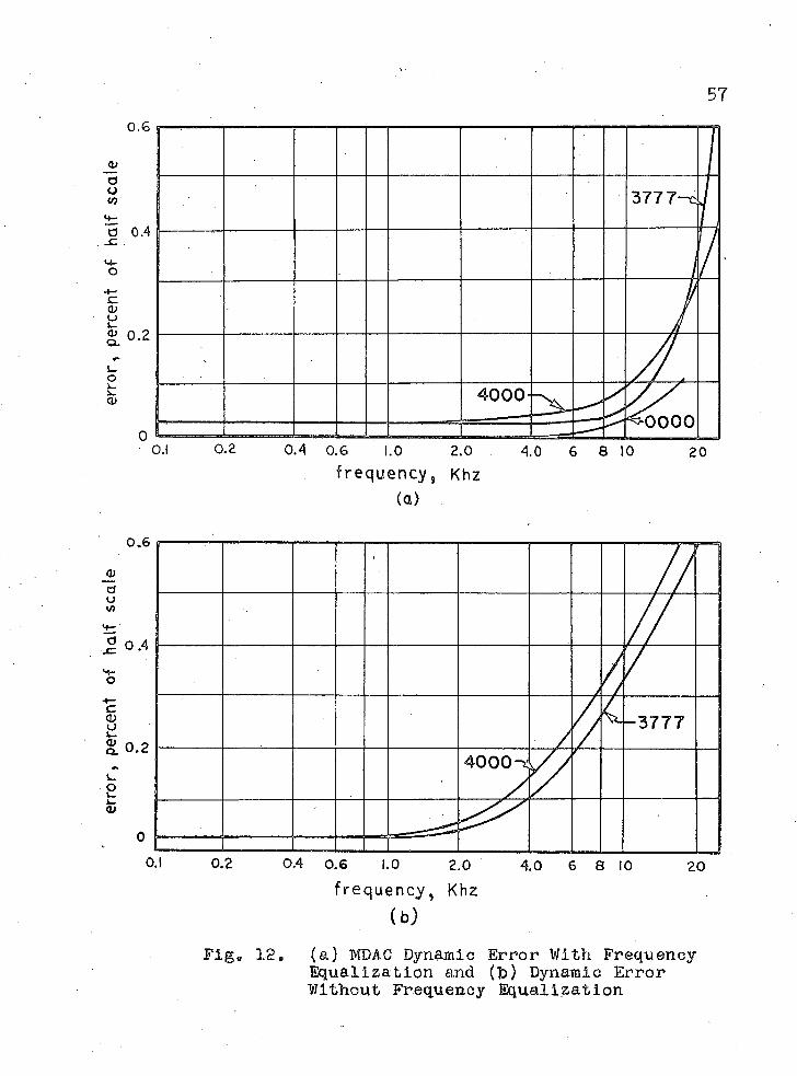
Simple fre^uency-response equalization techniques may be used to minimize output phase-shift error if desired© The feedback resistance of the operational amplifier is split into two 5K resistors, Phase-shift error may be minimized by inserting a capacitor from the center of the feedback resistance to ground (Fig, 2), This capacitor is chosen experimentally and has a value of lOpP. to 20 pF,.,.When equalization is used, the total MDAC dynamic error is> less than 0,1^ of -half scale at computing frequencies of 10 Khz (Fig, 12a)6
Errors Caused by Switching; Spikes The gate-to-drain junction capacitances of field,
effect transistors cause current spikes at the summing junction when the FET is.switched, " The resulting output voltage spikes are not important in many high-speed hybrid computations., where MDACrs are most commonly used to change parameters in the RESET period between analog-computer runs© Switching—spike error would only come into consideration when switching is to occur many times during a computer run and when spike errors might integrate into cumulative errors. Even when used in these applications, the errors caused by switching spikes are usually negligible because of the extremely short duration of the spikes, ,

46Capacitors used to reduce switching spikes are
inserted at the summing junction rather than at the source of each FET to minimize their effect on frequency response* Because the maximum voltage swing at the summing junction is ilQO pV* the frequency-response error caused by the 55 pF equivalent capacitance of spike-compensating capacitors at the summing junction is less than 5,5 pV at 10 Khz*

• CONSTRUCTION,' TESTING, M D RESULTS
Each. MD.AC is mounted on tvjo 2 7/8 in. by 9 in®printed circuit cards, with the pov/er-supply filters and five most significant bits on one card, and with the seven least significant bits on the other. Separate digital and analog ground planes are utilized to prevent digital noise on the analog ground, to prevent high current flow in the analog ground, and to minimize resistance in the analog ground. Too much resistance in the analog ground couldcause potential variation along the ground plane whichwould lead to errors in..binary weighting of the transfer impedances in the bits using T-networlcs. Both power supplies are filtered with pi-network filters to keep the switch-transients away from the LOCUST power supply.
The two HDAC cards mount in a p"xlO"xl" shielded can which plugs directly into the LOCUST analog patchbay. This eliminates all analog wiring between the patchbay and the HDAC. The can is a modified version of the 2nxlOnxln ■ can used for other LOCUST computing elements (Conant 1967)g with analog-signal and power supply-inputs at one end of the can, and a 12-pin connector for the 12 digital-signal lines at the other end. Trimmer potentiometers are .mounted so that they may be adjusted externally for calibration -of binary weighting after the HDAC is in place in the computer.
47

48The fully assembled MDAC is shewn, in Fig. 7» The
operational amplifier is not included in the MDAC can, but. it is patched externally on the analog patchbay and is thus available for other uses when MDAC1s are not in operation» The feedback network, however, is. included in the MDAC card®' A fuse is placed in the amplifier input lead (G8) to protect the switches in the event of erroneous patching® Because the fuse is inside the amplifier feedback loop, its resistance causes negligible error® Analog patching on the LOCUST patchbay is shown in Fig® 8® Two analog inputs, and
, are required, and an uncommitted amplifier is patched externally with its summing junction at G-’ and its output at 01® Four MDAC channels are included in the LOCUST system®
• -■ ' CalibrationCalibration of the MDAC is done with the device
installed in the computer® Either a flO volt or a -10 volt input is applied to both the -s-X and -X inputs on the analog patchbay® Calibration of binary.weighting proceeds from the least significant bit to the most significant bit®To calibrate a given bit, the digital input is switched repeatedly from a digital ”1” in the bit to be calibrated to digital ”lH:s'in all less significant bits® All other bits are at digital ,30!\® The difference in MDAC output voltage'for the two digital numbers should be 1 LSB, or 4®9 mv®, in all cases® The calibrating procedure thus

49consists of adjusting the trimmer in that bit until the correct voltage difference is obtained»
After binary weighting has been calibrated, the feedback resistor is matched to the resistance of the first bit* The feedback resistor is chosen by patching the feedback resistance which is to.be tested from the amplifier output 0 to the .summing junction G-, with 0* open circuited* The digital state of the MDAC is set to octal 4000* The feedback resistance is then selected or padded to. obtain exactly flO volts at the amplifier output for -10 volts at the fX analog input®
When static weighting and accuracy have been calibrated, dynamic error can be minimized by using one of the summing amplifiers in the analog computer as in Fig. 9®For an input of 10 sin wt, the summing amplifier output yields a convenient measure of dynamic error. Dynamic error is minimized by selecting the capacitor from ground to the center of the feedback resistance (Fig. 2) so that the output of the summing amplifier at 10 Khz has minimum magnitude variation from the output magnitude at 10 hz. Digital input to the MDAC is octal 3777 = Because the output frequency response at octal 4000 is similar to that at 37774 this procedure also provides frequency response compensation for bit 0®

50
Figo To Fully Assembled, MDAO
DA / MU
Figo 80 MDAG Terminals On LOCUST Analog Fatohbay
lOsin ut error
Figo 9o Circuit, For Measuring MDAC Dynamic Error

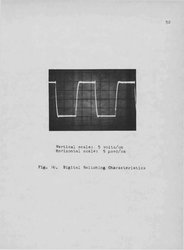
Digital Switching.Characteristics Switching delay for both the JFET and MOSFET switch
is less than 40^4secc Settling time (to within 0.025/? of half scale) at the MDAC output is less than 5 jusec with all switches changing state, and worst-case, rise and fall times when switched between tlO volts and -10 volts' are less than loSjuseco
Figure 10 shows the MDAG output for a 10 volt d@Ce analog input with digital states switching between octal 4000 and 3777 as an illustration of worst-case rise and fall time. Output voltage plus transient spikes remain
jless than -10,5 volts, so that the operational amplifier cannot overload because of switching spikes, .•
Figure 11a shows the switching spikes at the MDJkG output for a typical JFET switch. The upper trace is the output voltage with X^-0, and the lower trace is the digital drive signal at the switch input. The transient at the left is the turn-on-spike, while the turn-off spike appears at the right. Figure lib shows switching spikes for a typical MOSFET switch, and Fig, 11c shows worst-case switching spikes occuring when all 12 switches change states, The worst-case switching spike is.-2,8 volts,
- ■ " " 'Dynamic Characteristics " ' '' Figure 12a shows MDAC dynamic error as a function
of. frequency for digital states 4000, 3777? and 0000 with
Vertical scale: 5 volts/cmHorizontal scale: 5 paec/cm
10. Digital Switching Characteristics

53
Vertical scale: 0.5 volts/cmHorizontal scale: 1 nsec/cm
(a)
Vertical scale: 0.5 volts/cmHorizontal scale: 1 ^sec/cm
(b)
Fig. 11, MDAC Switching Spikes

Vertical scale: 2 volts/cmHorizontal scale: 1 /jsec/cm
(c)
Fig. 11, Continued. MDAC Switching Spikes

55frequency response equalization of the feedback impedance« Total error is within the LOCUST specification of Oolfo at 10 Khz, Error is shown in per cent of half-scale for an analog input of 10 sin w t 6 Error at 0000 is caused by feedthrough in capacitance of the MDAC circuit card«,
Figure 12b shows MDAC dynamic error for digital states 4000 and 3777 when the frequency response equalizing capacitor is not used* Error is 0»k% at 10 Khz - for. the uncompensated case«. In comparison, the phase-shift error of the LOCUST operational amplifier when used as a unity- gain,pha.se inverter - with 10K ohm impedances is 0*15^ at 10 Khz (Conant 1967) o'
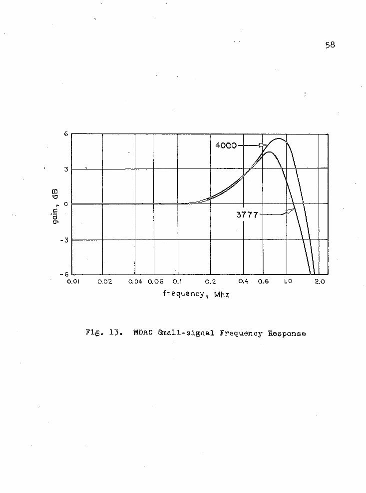
Small-signal frequency response of the MDAC is shown in Fig. 13 for digital states 4000 and 3777® Measurements' were made using an analog input of. 0.1 sin cut®- Frequency response is 3 db, down at 1.5 Mhz,,, while .fre-' . quency response of the LOCUST operational amplifier in a 10K Unity gain inverter is 3 db. down at 4.5 Mhz (Conant 1967)o '
Temperature drift of binary resolution was measured from•25°C to 45°C for the worst-case state of octal 7777s (all switches ON) with ah analog reference of +10 volts® Drift was less than 0.02,LSB/°C over the 20°C temperature range. . • ■ - - ' n . ' ' »

56. MDAC analog output response to a fast-rise-tlme -10
volt square wave applied to the an a lop; Input from a low. impedance source, with the MDAC in digital state 3777, had a rise time of less than 2 microsecondss an overshoot of 7^, and a settling time (within 0»1^) of approximately 4 microseconds «,
The upper trace of Fig. 14 shows the MDAC output for a 10 volt, 10 Khz» sine wave at the analog input multiplied by. a digitally-generated ramp.operating at maximum PDF-9 output speed. The lower trace shows MDAC output for the;same. 10 Khz- analog input with slowly-stepped digital attenuation© '
Figure 16 shows MDAC output for a 10 volt d.c© analog input with digital steps from 7773. to 0005, illus-. trading MDAC monotonicity as the digital input changes sign and all switches change state©
erro
r,
perc
ent
of ha
lf sc
ale
erro
r, pe
rcen
t of
half
scal
e57
0.6
0 0.2 0.4 0.60.1 4.0 6 8 10f r e q u e n c y , Khz
(a)0.6
4 0 0 0
0.4 0.60.2 1.0 4.0 6 8 10f r e q u e n c y , Khz
(b)Fige 12. (a) MDAC Dynamic Error With Frequency
Equalization and (t>) Dynamic Error Without Frequency Equalization
gain
, dB
58
3777
-3
-60.01 0.02 0.04 0.06 0.1 0.2 0.4 0.6 1.0 2.0f r e q u e n c y , Mhz
Figo 13o MDAC Small-signal Frequency Response

59
i
Vertical scale: 10 volta/cmHorizontal scale: 2 msec/cm
Fig, 14. MDAC Operation at Computer Speed
rT'
Vertical scale: 20 mV/cmHorizontal scale: 10 msec/cm
Fig. 15#- MDAC Resolution Near Digital Zero

REFERENCES
Conant, B ,.K® • "The Design of a New Solid State Electronic Interative Differential Analyzer Making Maximum Use of Integrated Circuits,11 EhuD Dissertation, Department of Electrical Engineering, University of Arizona, 1968»
Korn, G-e A., and T. Me Korne Electronic Analogand Hybrid Computers, McGraw-Hill .Book"Company, New York, 1964*
05Grady, E» P «, "Design, Test, and Applicationof a Hybrid Computer Interface,11 PhoD. Dissertation, 'Department of Electrical Engineering, University of Arizona, 1969«
.Pearman, C. R®, and A® Ee Popodi, "How To Design High-Speed D-A," Electronics, pp» 28 - 32, February 21, .1964«
Schmid, H* "Electronic Analog Switches," Electro- Technology, pp® 35 - 50, June, 19686 j
Shipley, M. "Analog ShJitching Circuits Use Field- Effect Devices, Electronics, pp. 45 ~ 50, December 28, 1964®
Wilkins, J. "Design and Test of a Hybrid Computer Interface," M® S® Thesis, Department of Electrical Engineering, University of Arizona, 1969®
60