Embed Size (px)
Citation preview
A CirCuit for All SeASonS
Behzad Razavi
IEEE SOLID-STATE CIRCUITS MAGAZINE fall 20 17 13
TThe decision-feedback equalizer (DFE) dates back to the 1960s [1] and be gan to appear in high-speed wireline com -munication systems in the early 2000s. In this article, we study the properties of this circuit and describe its “ana-log” implementations.
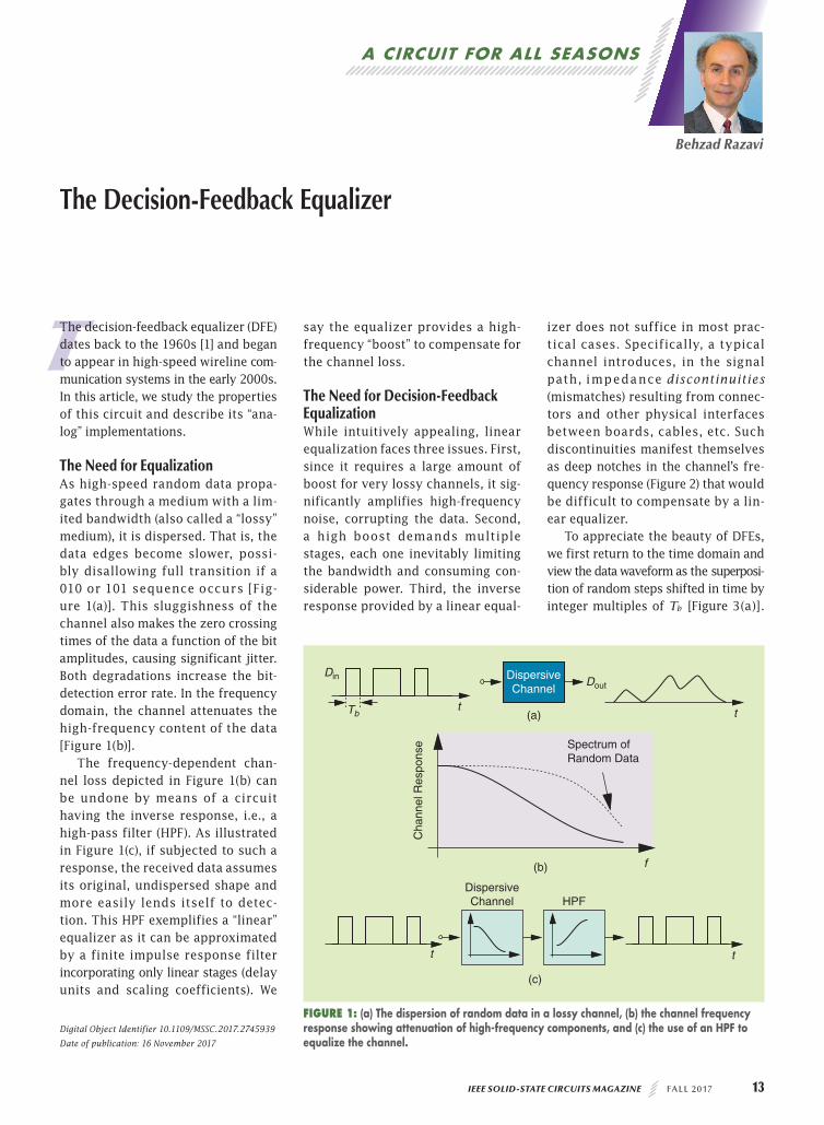
The Need for EqualizationAs high-speed random data propa-gates through a medium with a lim-ited bandwidth (also called a “lossy” medium), it is dispersed. That is, the data edges become slower, possi-bly disallowing full transition if a 010 or 101 sequence occurs [Fig-ure 1(a)]. This sluggishness of the channel also makes the zero crossing times of the data a function of the bit amp litudes, causing significant jitter. Both degradations increase the bit-detection error rate. In the frequency domain, the channel attenuates the high-frequency content of the data [Figure 1(b)].
The frequency-dependent chan-nel loss depicted in Figure 1(b) can be undone by means of a circuit having the inverse response, i.e., a high-pass filter (HPF). As illustrated in Figure 1(c), if subjected to such a response, the received data assumes its original, undispersed shape and more easily lends itself to detec-tion. This HPF exemplifies a “linear” equalizer as it can be approximated by a finite impulse response filter incorporating only linear stages (delay units and scaling coefficients). We
say the equalizer provides a high-frequency “boost” to compensate for the channel loss.
The Need for Decision-Feedback EqualizationWhile intuitively appealing, linear equalization faces three issues. First, since it requires a large amount of boost for very lossy channels, it sig-nificantly amplifies high-frequency noise, corrupting the data. Second, a high boost demands multiple stages, each one inevitably limiting the bandwidth and consuming con-siderable power. Third, the inverse response provided by a linear equal-
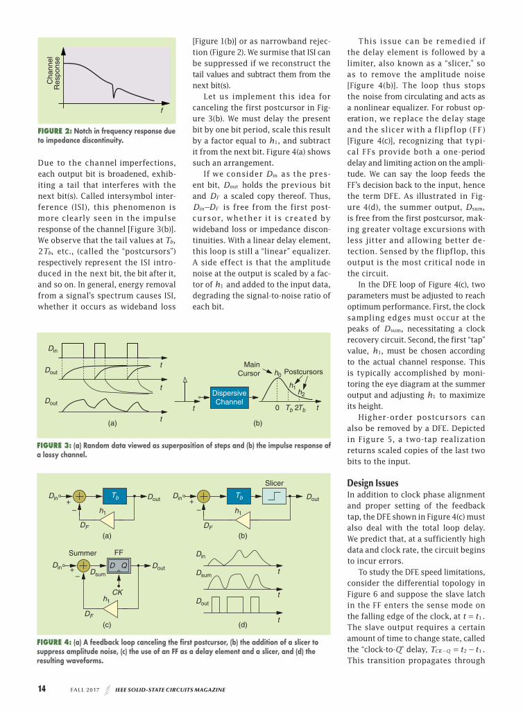
izer does not suffice in most prac-tical cases. Specifically, a typical channel introduces, in the signal path, impedance discontinuities (mismatches) resulting from connec-tors and other physical interfaces between boards, cables, etc. Such discontinuities manifest themselves as deep notches in the channel’s fre -quency response (Figure 2) that would be difficult to compensate by a lin-ear equalizer.
To appreciate the beauty of DFEs, we first return to the time domain and view the data waveform as the superposi-tion of random steps shifted in time by integer multiples of Tb [Figure 3(a)].
The Decision-Feedback Equalizer
Digital Object Identifier 10.1109/MSSC.2017.2745939
Date of publication: 16 November 2017
(a)
DispersiveChannel
Din Dout
Tb tt
Cha
nnel
Res
pons
e Spectrum ofRandom Data
(b) f
(c)
DispersiveChannel HPF
t t
Figure 1: (a) the dispersion of random data in a lossy channel, (b) the channel frequency response showing attenuation of high-frequency components, and (c) the use of an HPf to equalize the channel.
14 fall 20 17 IEEE SOLID-STATE CIRCUITS MAGAZINE
Due to the channel imperfections, each output bit is broadened, exhib-iting a tail that interferes with the next bit(s). Called intersymbol inter-ference (ISI), this phenomenon is more clearly seen in the impulse response of the channel [Figure 3(b)]. We observe that the tail values at ,Tb
,T2 b etc., (called the “postcursors”) respectively represent the ISI intro-duced in the next bit, the bit after it, and so on. In general, energy removal from a signal’s spectrum causes ISI, whether it occurs as wideband loss
[Figure 1(b)] or as narrowband rejec-tion (Figure 2). We surmise that ISI can be suppressed if we reconstruct the tail values and subtract them from the next bit(s).
Let us implement this idea for canceling the first postcursor in Fig-ure 3(b). We must delay the present bit by one bit period, scale this result by a factor equal to ,h1 and subtract it from the next bit. Figure 4(a) shows such an arrangement.
If we consider Din as the pres-ent bit, Dout holds the previous bit and DF a scaled copy thereof. Thus, D DFin- is free from the first post-cursor, whether it is created by wideband loss or impedance discon-tinuities. With a linear delay element, this loop is still a “linear” equalizer. A side effect is that the amplitude noise at the output is scaled by a fac-tor of h1 and added to the input data, degrading the signal-to-noise ratio of each bit.
This issue can be remedied if the delay element is followed by a limiter, also known as a “slicer,” so as to remove the amplitude noise [Figure 4(b)]. The loop thus stops the noise from circulating and acts as a nonlinear equalizer. For robust op -eration, we replace the delay stage and the slicer with a f lipflop (FF) [Figure 4(c)], recognizing that typi-cal FFs provide both a one-period delay and limiting action on the ampli-tude. We can say the loop feeds the FF’s decision back to the input, hence the term DFE. As illustrated in Fig-ure 4(d), the summer output, ,Dsum is free from the first postcursor, mak-ing greater voltage excursions with less jitter and allowing better de -tection. Sensed by the flipflop, this output is the most critical node in the circuit.
In the DFE loop of Figure 4(c), two parameters must be adjusted to reach optimum performance. First, the clock sampling edges must occur at the peaks of ,Dsum necessitating a clock recovery circuit. Second, the first “tap” value, ,h1 must be chosen according to the actual channel response. This is typically accomplished by moni-toring the eye diagram at the summer output and adjusting h1 to maximize its height.
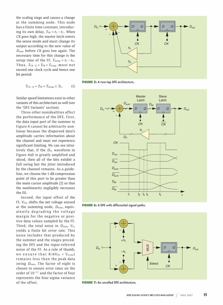
Higher-order postcursors can also be removed by a DFE. Depicted in Figure 5, a two-tap realization returns scaled copies of the last two bits to the input.
Design IssuesIn addition to clock phase alignment and proper setting of the feedback tap, the DFE shown in Figure 4(c) must also deal with the total loop delay. We predict that, at a sufficiently high data and clock rate, the circuit begins to incur errors.
To study the DFE speed limitations, consider the differential top ology in Figure 6 and suppose the slave latch in the FF enters the sense mode on the falling edge of the clock, at .t t1= The slave output requires a certain amount of time to change state, called the “clock-to-Q” delay, .T t tCK Q 2 1= -- This transition propagates through
Cha
nnel
Res
pons
e
f
Figure 2: notch in frequency response due to impedance discontinuity.
Slicer
FF
(c) (d)
(a) (b)
Summer
Din
Din
DinDsum Dsum
DinDout
Dout
Dout
Dout
DF
DF
DF
+
+
–
–
–+
h1
h1
h1
Tb Tb
D Q
CK
t
t
t
Figure 4: (a) A feedback loop canceling the first postcursor, (b) the addition of a slicer to suppress amplitude noise, (c) the use of an ff as a delay element and a slicer, and (d) the resulting waveforms.
DispersiveChannel
MainCursor Postcursors
Din
Dout
Dout
t
t
t t
t
h0
h1h2
0 Tb 2Tb
(a) (b)
Figure 3: (a) random data viewed as superposition of steps and (b) the impulse response of a lossy channel.
IEEE SOLID-STATE CIRCUITS MAGAZINE fall 20 17 15
the scaling stage and causes a change at the summing node. This node has a finite time constant, introduc-ing its own delay, .T t tFB 3 2= - When CK goes high, the master latch enters the sense mode and must change its output according to the new value of Dsum before CK goes low again. The necessary time for this change is the setup time of the FF, .T t t5 4setup = - Thus, T T TCK Q FB setup+ +- must not exceed one clock cycle and hence one bit period:
.T T T TCK Q FB bsetup #+ +- (1)
Similar speed limitations exist in other variants of this architecture as well (see the “DFE Variants” section).
Three other nonidealities affect the performance of the DFE. First, the data input port of the summer in Figure 6 cannot be arbitrarily non-linear because the dispersed data’s amplitude carries information about the channel and must not experience significant limiting. We can see intui-tively that, if the Din waveform in Figure 4(d) is greatly amplified and sliced, then all of the bits exhibit a full swing but the jitter introduced by the channel remains. As a guide-line, we choose the 1-dB compression point of this port to be greater than the main cursor amplitude [2] so that the nonlinearity negligibly increases the ISI.
Second, the input offset of the FF, ,VOS shifts the net voltage sensed at the summing node, ,Dsum equiv -alent ly deg rad ing the volt age margin for the negative or posi-tive data values sampled by the FF. Third, the total noise in ,Dsum ,Vn yields a finite bit error rate. This noise includes that produced by the summer and the stages preced-ing the DFE and the input-referred noise of the FF. As a rule of thumb, w e e n s u r e t h a t ( )V V8 4 ,nOS rms+ remains less than the peak data swing .Dsum The factor of eight is chosen to ensure error rates on the order of 10 12- and the factor of four represents the four-sigma variance of the offset.
Din
+
+
–
–
+h1
–h1
MU
X
D Q Dout
SelectCK
Figure 7: An unrolled Dfe architecture.
MasterLatch
SlaveLatch
Din Dout
Dout
Dout
Dsum
Dsum
DM
DM
Dsum DM
+–
D Q D Q
CK
CKCK
h1
DF
t1 t2 t3 t4 t5 t
Figure 6: A Dfe with differential signal paths.
Din Dout+
––
D Q D Q
h1
h2
CK CK
Figure 5: A two-tap Dfe architecture.
16 fall 20 17 IEEE SOLID-STATE CIRCUITS MAGAZINE
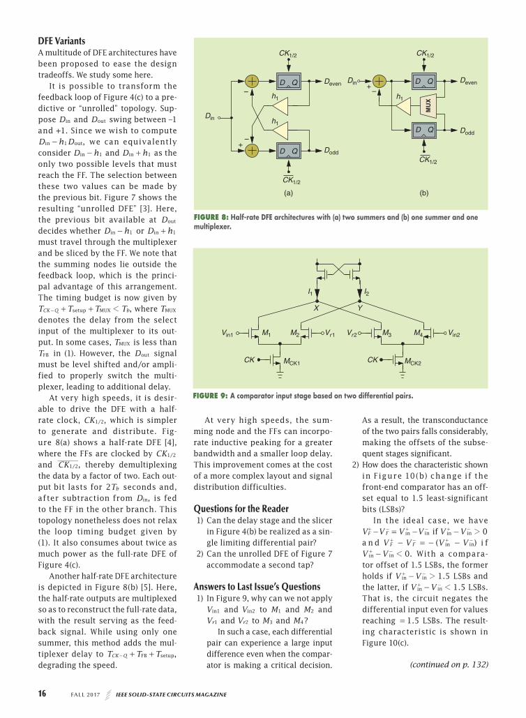
DFE VariantsA multitude of DFE architectures have been proposed to ease the design tradeoffs. We study some here.
It is possible to transform the feedback loop of Figure 4(c) to a pre-dictive or “unrolled” topology. Sup-pose Din and Dout swing between –1 and +1. Since we wish to compute
,D h D1in out- we can equivalently consider D h1in- and D h1in+ as the only two possible levels that must reach the FF. The selection between these two values can be made by the previous bit. Figure 7 shows the resulting “unrolled DFE” [3]. Here, the previous bit available at Dout decides whether D h1in- or D h1in+ must travel through the multiplexer and be sliced by the FF. We note that the summing nodes lie outside the feedback loop, which is the princi-pal advantage of this arrangement. The timing budget is now given by
,T T T TCK Q bsetup MUX 1+ +- where TMUX denotes the delay from the select input of the multiplexer to its out-put. In some cases, TMUX is less than TFB in (1). However, the Dout signal must be level shifted and/or ampli-fied to properly switch the multi-plexer, leading to additional delay.
At very high speeds, it is desir-able to drive the DFE with a half-rate clock, ,CK /1 2 which is simpler to generate and distribute. Fig-ure 8(a) shows a half-rate DFE [4], where the FFs are clocked by CK /1 2 and ,CK /1 2 thereby demultiplexing the data by a factor of two. Each out-put bit lasts for T2 b seconds and, after subtraction from ,Din is fed to the FF in the other branch. This topology nonetheless does not re lax the loop timing budget given by (1). It also consumes about twice as much power as the full-rate DFE of Figure 4(c).
Another half-rate DFE architecture is depicted in Figure 8(b) [5]. Here, the half-rate outputs are multiplexed so as to reconstruct the full-rate data, with the result serving as the feed-back signal. While using only one summer, this method adds the mul-tiplexer delay to ,T T TCK Q FB setup+ +- degrading the speed.
At very high speeds, the sum-ming node and the FFs can incorpo-rate inductive peaking for a greater bandwidth and a smaller loop delay. This improvement comes at the cost of a more complex layout and signal distribution difficulties.
Questions for the Reader1) Can the delay stage and the slicer
in Figure 4(b) be realized as a sin-gle limiting differential pair?
2) Can the unrolled DFE of Figure 7 accommodate a second tap?
Answers to Last Issue’s Questions1) In Figure 9, why can we not apply
V 1in and V 2in to M1 and M2 and Vr1 and Vr2 to M3 and ?M4
In such a case, each differential pair can experience a large input difference even when the compar-ator is making a critical decision.
As a result, the transconductance of the two pairs falls considerably, making the offsets of the subse-quent stages significant.
2) How does the characteristic shown in Figure 10(b) change if the front-end comparator has an off-set equal to 1.5 least-significant bits (LSBs)?
In the ideal case, we have V V V VF F in in- = -+ - + - if V V 0in in 2-+ - a n d ( )V V V VF F in in- = - -+ - + - i f
.V V 0in in 1-+ - With a compara-tor offset of 1.5 LSBs, the former holds if .V V 1 5in in 2-+ - LSBs and the latter, if .V V 1 5in in 1-+ - LSBs. That is, the circuit negates the differential input even for values reaching .1 5= LSBs. The result-ing characteristic is shown in Figure 10(c).
MUX
Din
DinDeven
Dodd
Deven
Dodd
+
+
– –
–
D Q
D Q
D Q
D Q
h1 h1
h1
CK1/2 CK1/2
CK1/2
CK1/2
(a) (b)
Figure 8: Half-rate Dfe architectures with (a) two summers and (b) one summer and one multiplexer.
M1 M2 M3 M4
MCK1CK
Vin1 Vin2Vr1
X Y
MCK2CK
Vr2
I1 I2
Figure 9: A comparator input stage based on two differential pairs.
(continued on p. 132)
132 fall 20 17 IEEE SOLID-STATE CIRCUITS MAGAZINE
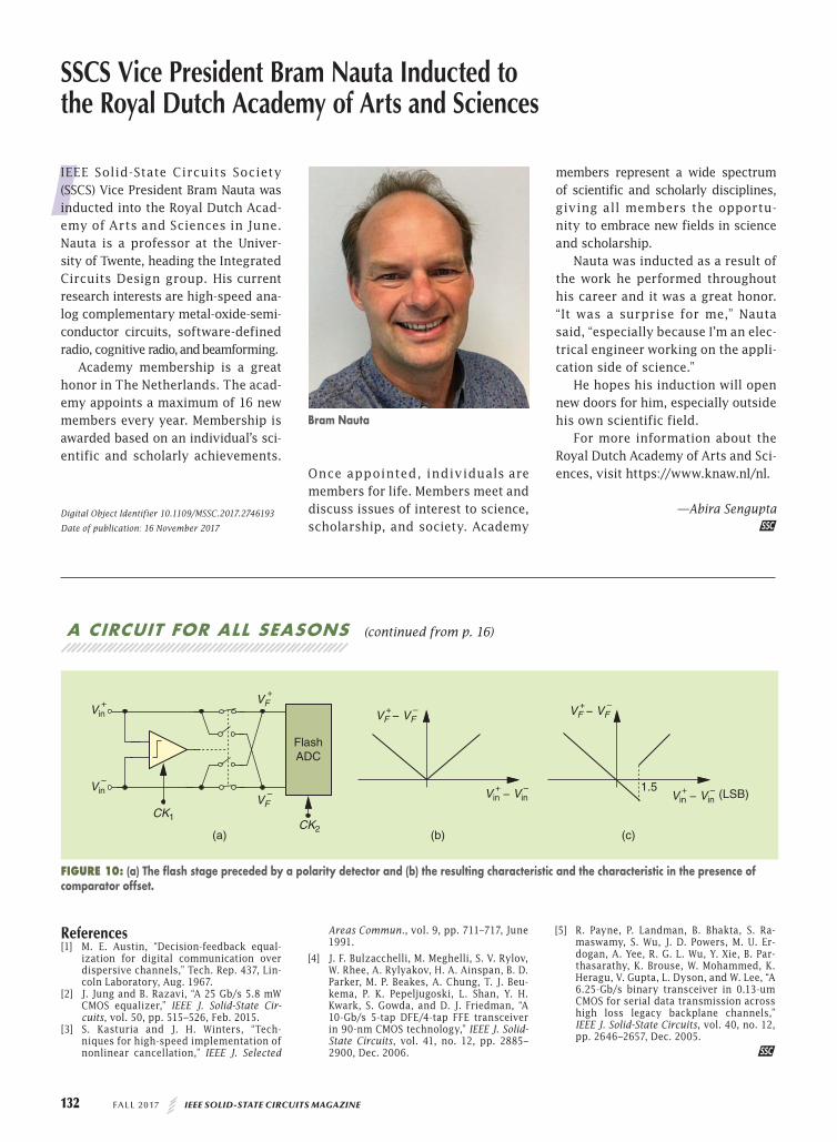
IIEEE Solid-State Circuits Society (SSCS) Vice President Bram Nauta was inducted into the Royal Dutch Acad-emy of Arts and Sciences in June. Nauta is a professor at the Univer-sity of Twente, heading the Integrated Circuits Design group. His current research interests are high-speed ana-log complementary metal-oxide-semi-conductor circuits, software-defined radio, cognitive radio, and beamforming.
Academy membership is a great honor in The Netherlands. The acad-emy appoints a maximum of 16 new members every year. Membership is awarded based on an individual’s sci -entific and scholarly achievements.
Once appointed, individuals are members for life. Members meet and discuss issues of interest to science, scholarship, and society. Academy
members represent a wide spectrum of scientific and scholarly disciplines, giving all members the opportu-nity to embrace new fields in science and scholarship.
Nauta was inducted as a result of the work he performed throughout his career and it was a great honor. “It was a surprise for me,” Nauta said, “especially because I’m an elec-trical engineer working on the appli-cation side of science.”
He hopes his induction will open new doors for him, especially outside his own scientific field.
For more information about the Royal Dutch Academy of Arts and Sci-ences, visit https://www.knaw.nl/nl.
—Abira Sengupta
bram nauta
a cIRcuIt FoR aLL seasons (continued from p. 16)
Vin+
Vin–
FlashADC
CK1CK2
VF+
VF–
+ –VF − VF+ –VF − VF
+ –Vin − Vin
(a) (b)
1.5
(c)
+ –Vin − Vin (LSB)
Figure 10: (a) the flash stage preceded by a polarity detector and (b) the resulting characteristic and the characteristic in the presence of comparator offset.
References[1] M. E. Austin, “Decision-feedback equal-
ization for digital communication over dispersive channels,” Tech. Rep. 437, Lin-coln Laboratory, Aug. 1967.
[2] J. Jung and B. Razavi, “A 25 Gb/s 5.8 mW CMOS equalizer,” IEEE J. Solid-State Cir-cuits, vol. 50, pp. 515–526, Feb. 2015.
[3] S. Kasturia and J. H. Winters, “Tech-niques for high-speed implementation of nonlinear cancellation,” IEEE J. Selected
Areas Commun., vol. 9, pp. 711–717, June 1991.
[4] J. F. Bulzacchelli, M. Meghelli, S. V. Rylov, W. Rhee, A. Rylyakov, H. A. Ainspan, B. D. Parker, M. P. Beakes, A. Chung, T. J. Beu-kema, P. K. Pepeljugoski, L. Shan, Y. H. Kwark, S. Gowda, and D. J. Friedman, “A 10-Gb/s 5-tap DFE/4-tap FFE transceiver in 90-nm CMOS technology,” IEEE J. Solid-State Circuits, vol. 41, no. 12, pp. 2885–2900, Dec. 2006.
[5] R. Payne, P. Landman, B. Bhakta, S. Ra-maswamy, S. Wu, J. D. Powers, M. U. Er-dogan, A. Yee, R. G. L. Wu, Y. Xie, B. Par-thasarathy, K. Brouse, W. Mohammed, K. Heragu, V. Gupta, L. Dyson, and W. Lee, “A 6.25-Gb/s binary transceiver in 0.13-um CMOS for serial data transmission across high loss legacy backplane channels,” IEEE J. Solid-State Circuits, vol. 40, no. 12, pp. 2646–2657, Dec. 2005.
SSCS Vice President Bram Nauta Inducted to the Royal Dutch Academy of Arts and Sciences
Digital Object Identifier 10.1109/MSSC.2017.2746193
Date of publication: 16 November 2017