Embed Size (px)
Citation preview
Data SheetData Sheet
Multilayer ceramic capacitors
Date: October 2006
EPCOS AG 2006. Reproduction, publication and dissemination of this data sheet and theinformation contained therein without EPCOS’ prior express consent is prohibited.
Chip capacitors, C0G
2 10/06Please read Cautions and warnings andImportant notes at the end of this document.
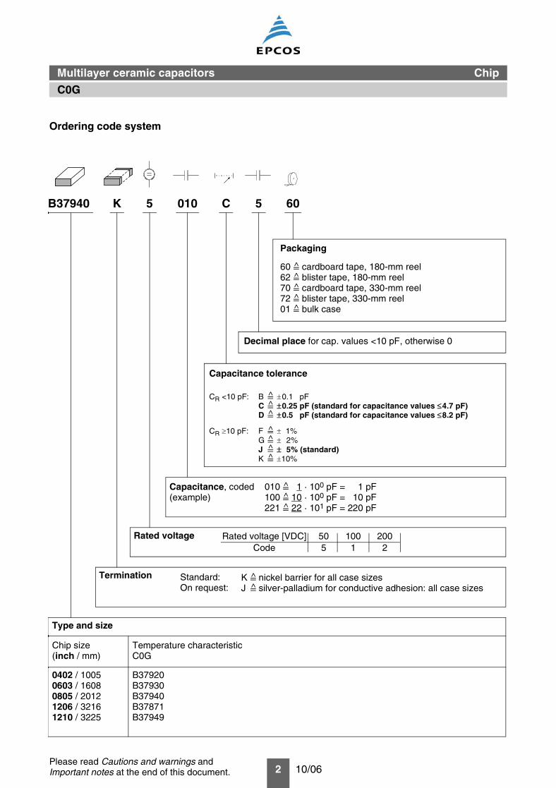
Ordering code system
B37940 K 5 010 C 5 60
Packaging
60 cardboard tape, 180-mm reel62 blister tape, 180-mm reel70 cardboard tape, 330-mm reel72 blister tape, 330-mm reel01 bulk case
^^^^^
Decimal place for cap. values <10 pF, otherwise 0
Capacitance tolerance
B 0.1 pFC ±0.25 pF (standard for capacitance values ≤4.7 pF)D ±0.5 pF (standard for capacitance values ≤8.2 pF)
^^^
F 1%G 2%J ± 5% (standard)K 10%
^^^^
CR <10 pF:
CR 10 pF:
Capacitance, coded(example)
010 1 · 100 pF = 1 pF100 10 · 100 pF = 10 pF221 22 · 101 pF = 220 pF
^^^
Rated voltage Rated voltage [VDC]Code
50 100 2005 1 2
Termination
Type and size
Chip size(inch / mm)
0402 / 10050603 / 16080805 / 20121206 / 32161210 / 3225
Temperature characteristicC0G
B37920B37930B37940B37871B37949
Standard:On request:
K nickel barrier for all case sizesJ silver-palladium for conductive adhesion: all case sizes
^^
Chip
C0G
Multilayer ceramic capacitors
3 10/06Please read Cautions and warnings andImportant notes at the end of this document.
Features
Good thermal stability High insulation resistance Low dissipation factor Low inductance To AEC-Q200
Applications
Resonant circuits Filter circuits Timing elements Coupling and filtering, particularly in RF circuits
Termination
For soldering: Nickel barrier terminations (Ni) For conductive adhesion: Silver-palladium terminations (AgPd) on request
Options
Alternative capacitance tolerances available on request
Delivery mode
Cardboard and blister tape (blister tape for chip thickness 1.2 0.1 mm and case size 1210),180-mm and 330-mm reel available
Bulk case for case sizes 0402, 0603 (50 V) and 0805 (50 V) on request
Electrical data
Temperature characteristic C0GClimatic category (IEC 60068-1) 55/125/56Standard EIADielectric Class 1Rated voltage VR 50, 100, 200 VDCTest voltage Vtest 2.5 · VR/5 s VDCCapacitance range / E series CR 1 pF … 10 nF (E6/E12)Temperature coefficient 0 30 · 10–6/KDissipation factor (limit value) tan <1.0 · 10–3
Insulation resistance1) at + 25 C Rins >105 M
Insulation resistance1) at +125 C Rins >104 M
Time constant1) at + 25 C >1000 sTime constant1) at +125 C >100 sOperating temperature range Top –55 … +125 CAgeing none
1) For CR >10 nF the time constant = C · Rins is given.
Chip
C0G
Multilayer ceramic capacitors
Multilayer ceramic capacitors
4 10/06
C0G
Please read Cautions and warnings andImportant notes at the end of this document.
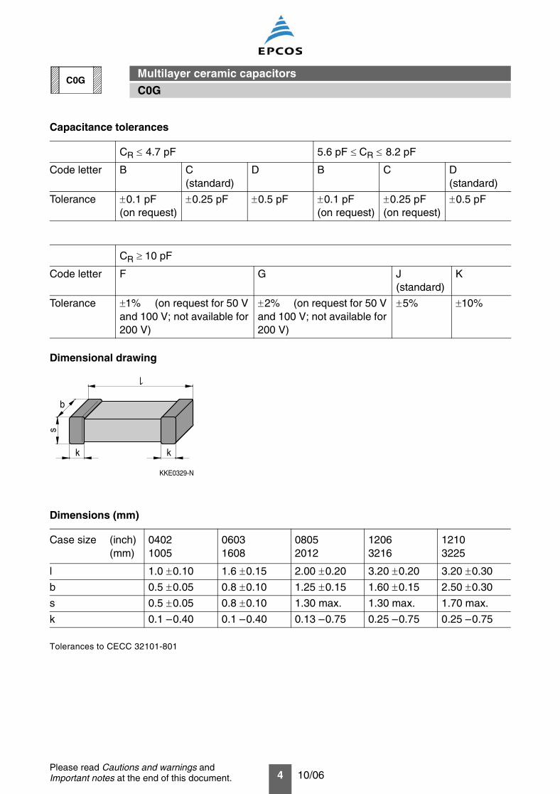
Capacitance tolerances
Dimensional drawing
Dimensions (mm)
Tolerances to CECC 32101-801
CR 4.7 pF 5.6 pF CR 8.2 pF
Code letter B C(standard)
D B C D(standard)
Tolerance 0.1 pF(on request)
0.25 pF 0.5 pF 0.1 pF(on request)
0.25 pF(on request)
0.5 pF
CR 10 pF
Code letter F G J(standard)
K
Tolerance 1% (on request for 50 V and 100 V; not available for 200 V)
2% (on request for 50 V and 100 V; not available for 200 V)
5% 10%
Case size (inch)(mm)
04021005
06031608
08052012
12063216
12103225
l 1.0 0.10 1.6 0.15 2.00 0.20 3.20 0.20 3.20 0.30
b 0.5 0.05 0.8 0.10 1.25 0.15 1.60 0.15 2.50 0.30
s 0.5 0.05 0.8 0.10 1.30 max. 1.30 max. 1.70 max.
k 0.1 –0.40 0.1 –0.40 0.13 –0.75 0.25 –0.75 0.25 –0.75
KKE0329-N
k
s
b
k
C0G
Multilayer ceramic capacitors
5 10/06
C0G
Please read Cautions and warnings andImportant notes at the end of this document.
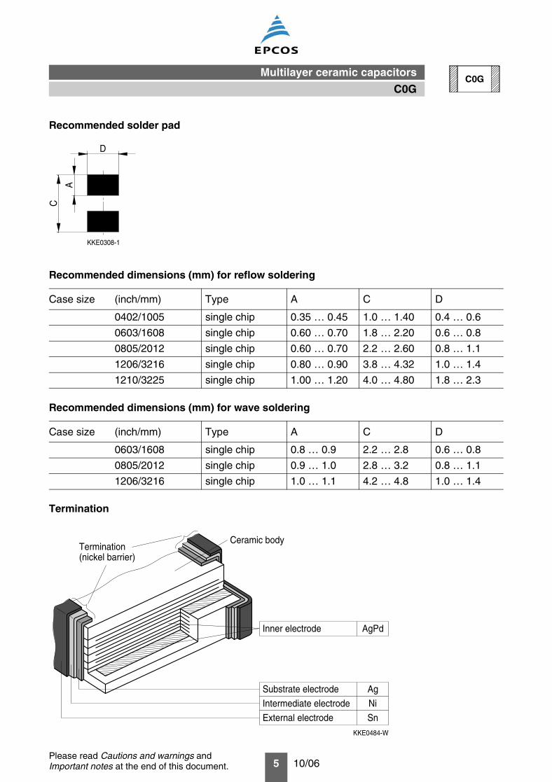
Recommended solder pad
Recommended dimensions (mm) for reflow soldering
Recommended dimensions (mm) for wave soldering
Termination
Case size (inch/mm) Type A C D
0402/1005 single chip 0.35 … 0.45 1.0 … 1.40 0.4 … 0.6
0603/1608 single chip 0.60 … 0.70 1.8 … 2.20 0.6 … 0.8
0805/2012 single chip 0.60 … 0.70 2.2 … 2.60 0.8 … 1.1
1206/3216 single chip 0.80 … 0.90 3.8 … 4.32 1.0 … 1.4
1210/3225 single chip 1.00 … 1.20 4.0 … 4.80 1.8 … 2.3
Case size (inch/mm) Type A C D
0603/1608 single chip 0.8 … 0.9 2.2 … 2.8 0.6 … 0.8
0805/2012 single chip 0.9 … 1.0 2.8 … 3.2 0.8 … 1.1
1206/3216 single chip 1.0 … 1.1 4.2 … 4.8 1.0 … 1.4
KKE0308-1
D
A
C
External electrode
Intermediate electrode
Substrate electrode
KKE0484-W
Ni
Sn
Ag
Inner electrode AgPd
Termination(nickel barrier)
Ceramic body
C0G
Multilayer ceramic capacitors
6 10/06
C0G
Please read Cautions and warnings andImportant notes at the end of this document.
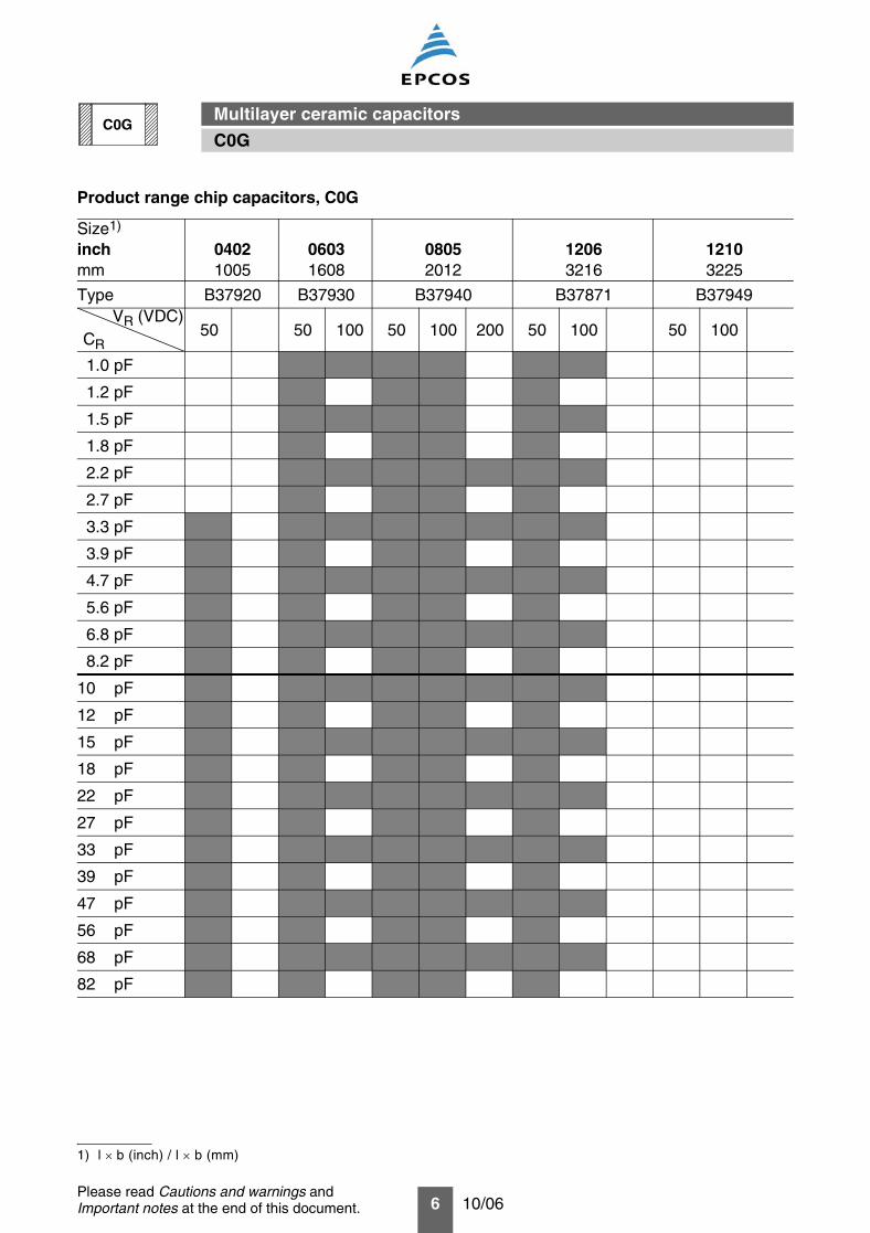
Product range chip capacitors, C0G
Size1)
inchmm
04021005
06031608
08052012
12063216
12103225
Type B37920 B37930 B37940 B37871 B37949
50 50 100 50 100 200 50 100 50 100
1.0 pF
1.2 pF
1.5 pF
1.8 pF
2.2 pF
2.7 pF
3.3 pF
3.9 pF
4.7 pF
5.6 pF
6.8 pF
8.2 pF
10 pF
12 pF
15 pF
18 pF
22 pF
27 pF
33 pF
39 pF
47 pF
56 pF
68 pF
82 pF
1) l b (inch) / l b (mm)
VR (VDC)CR
C0G
Multilayer ceramic capacitors
7 10/06
C0G
Please read Cautions and warnings andImportant notes at the end of this document.
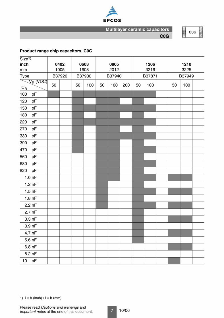
Product range chip capacitors, C0G
Size1)
inchmm
04021005
06031608
08052012
12063216
12103225
Type B37920 B37930 B37940 B37871 B37949
50 50 100 50 100 200 50 100 50 100
100 pF
120 pF
150 pF
180 pF
220 pF
270 pF
330 pF
390 pF
470 pF
560 pF
680 pF
820 pF
1.0 nF
1.2 nF
1.5 nF
1.8 nF
2.2 nF
2.7 nF
3.3 nF
3.9 nF
4.7 nF
5.6 nF
6.8 nF
8.2 nF
10 nF
1) l b (inch) / l b (mm)
VR (VDC)CR
C0G
Multilayer ceramic capacitors
8 10/06
C0G
Please read Cautions and warnings andImportant notes at the end of this document.
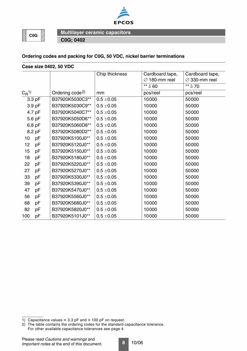
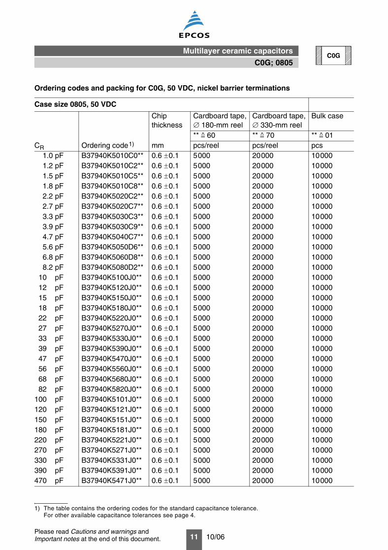
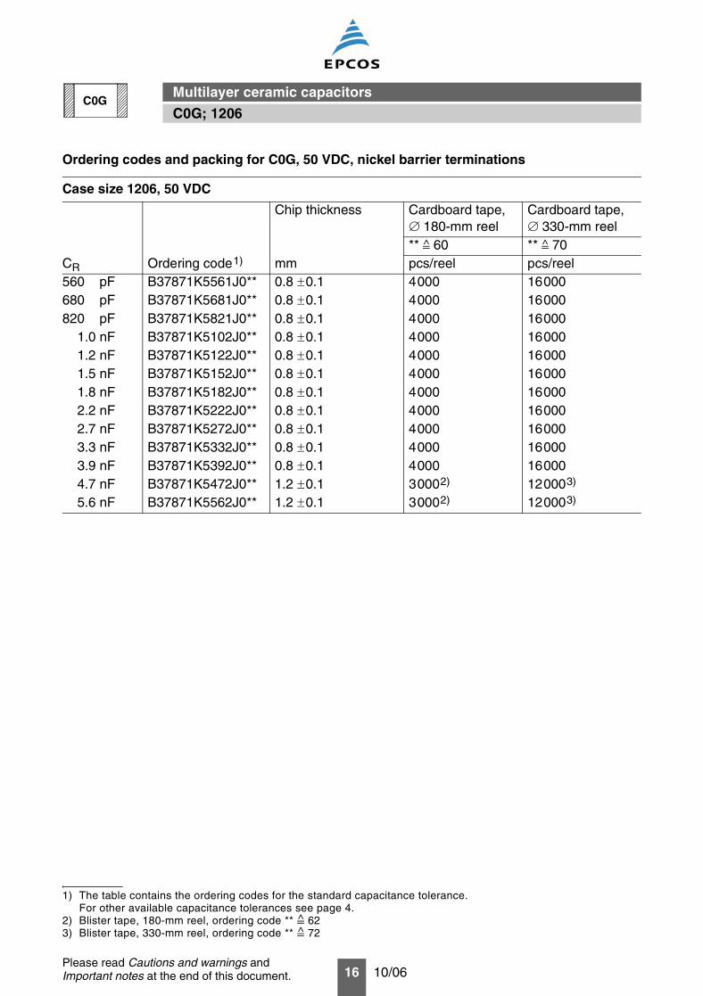
Ordering codes and packing for C0G, 50 VDC, nickel barrier terminations
Case size 0402, 50 VDC
Chip thickness Cardboard tape, 180-mm reel
Cardboard tape, 330-mm reel
** 60 ** 70CR
1) Ordering code2) mm pcs/reel pcs/reel3.3 pF B37920K5030C3** 0.5 0.05 10000 500003.9 pF B37920K5030C9** 0.5 0.05 10000 500004.7 pF B37920K5040C7** 0.5 0.05 10000 500005.6 pF B37920K5050D6** 0.5 0.05 10000 500006.8 pF B37920K5060D8** 0.5 0.05 10000 500008.2 pF B37920K5080D2** 0.5 0.05 10000 50000
10. pF B37920K5100J0** 0.5 0.05 10000 5000012. pF B37920K5120J0** 0.5 0.05 10000 5000015. pF B37920K5150J0** 0.5 0.05 10000 5000018. pF B37920K5180J0** 0.5 0.05 10000 5000022. pF B37920K5220J0** 0.5 0.05 10000 5000027. pF B37920K5270J0** 0.5 0.05 10000 5000033. pF B37920K5330J0** 0.5 0.05 10000 5000039. pF B37920K5390J0** 0.5 0.05 10000 5000047. pF B37920K5470J0** 0.5 0.05 10000 5000056. pF B37920K5560J0** 0.5 0.05 10000 5000068. pF B37920K5680J0** 0.5 0.05 10000 5000082. pF B37920K5820J0** 0.5 0.05 10000 50000
100. pF B37920K5101J0** 0.5 0.05 10000 50000
^ ^
1) Capacitance values < 3.3 pF and > 100 pF on request.2) The table contains the ordering codes for the standard capacitance tolerance.
For other available capacitance tolerances see page 4.
C0G; 0402

Multilayer ceramic capacitors
9 10/06
C0G
Please read Cautions and warnings andImportant notes at the end of this document.
Ordering codes and packing for C0G, 50 VDC, nickel barrier terminations
Case size 0603, 50 VDC
Chipthickness
Cardboard tape, 180-mm reel
Cardboard tape, 330-mm reel
Bulk case
** 60 ** 70 ** 01CR Ordering code1) mm pcs/reel pcs/reel pcs
1.0 pF B37930K5010C0** 0.8 0.1 4000 16000 150001.2 pF B37930K5010C2** 0.8 0.1 4000 16000 150001.5 pF B37930K5010C5** 0.8 0.1 4000 16000 150001.8 pF B37930K5010C8** 0.8 0.1 4000 16000 150002.2 pF B37930K5020C2** 0.8 0.1 4000 16000 150002.7 pF B37930K5020C7** 0.8 0.1 4000 16000 150003.3 pF B37930K5030C3** 0.8 0.1 4000 16000 150003.9 pF B37930K5030C9** 0.8 0.1 4000 16000 150004.7 pF B37930K5040C7** 0.8 0.1 4000 16000 150005.6 pF B37930K5050D6** 0.8 0.1 4000 16000 150006.8 pF B37930K5060D8** 0.8 0.1 4000 16000 150008.2 pF B37930K5080D2** 0.8 0.1 4000 16000 15000
10. pF B37930K5100J0** 0.8 0.1 4000 16000 1500012. pF B37930K5120J0** 0.8 0.1 4000 16000 1500015. pF B37930K5150J0** 0.8 0.1 4000 16000 1500018. pF B37930K5180J0** 0.8 0.1 4000 16000 1500022. pF B37930K5220J0** 0.8 0.1 4000 16000 1500027. pF B37930K5270J0** 0.8 0.1 4000 16000 1500033. pF B37930K5330J0** 0.8 0.1 4000 16000 1500039. pF B37930K5390J0** 0.8 0.1 4000 16000 1500047. pF B37930K5470J0** 0.8 0.1 4000 16000 1500056. pF B37930K5560J0** 0.8 0.1 4000 16000 1500068. pF B37930K5680J0** 0.8 0.1 4000 16000 1500082. pF B37930K5820J0** 0.8 0.1 4000 16000 15000
100. pF B37930K5101J0** 0.8 0.1 4000 16000 15000120. pF B37930K5121J0** 0.8 0.1 4000 16000 15000150. pF B37930K5151J0** 0.8 0.1 4000 16000 15000180. pF B37930K5181J0** 0.8 0.1 4000 16000 15000220. pF B37930K5221J0** 0.8 0.1 4000 16000 15000270. pF B37930K5271J0** 0.8 0.1 4000 16000 15000330. pF B37930K5331J0** 0.8 0.1 4000 16000 15000390. pF B37930K5391J0** 0.8 0.1 4000 16000 15000470. pF B37930K5471J0** 0.8 0.1 4000 16000 15000
1) The table contains the ordering codes for the standard capacitance tolerance.For other available capacitance tolerances see page 4.
^ ^ ^
C0G; 0603
Multilayer ceramic capacitors
10 10/06
C0G
Please read Cautions and warnings andImportant notes at the end of this document.
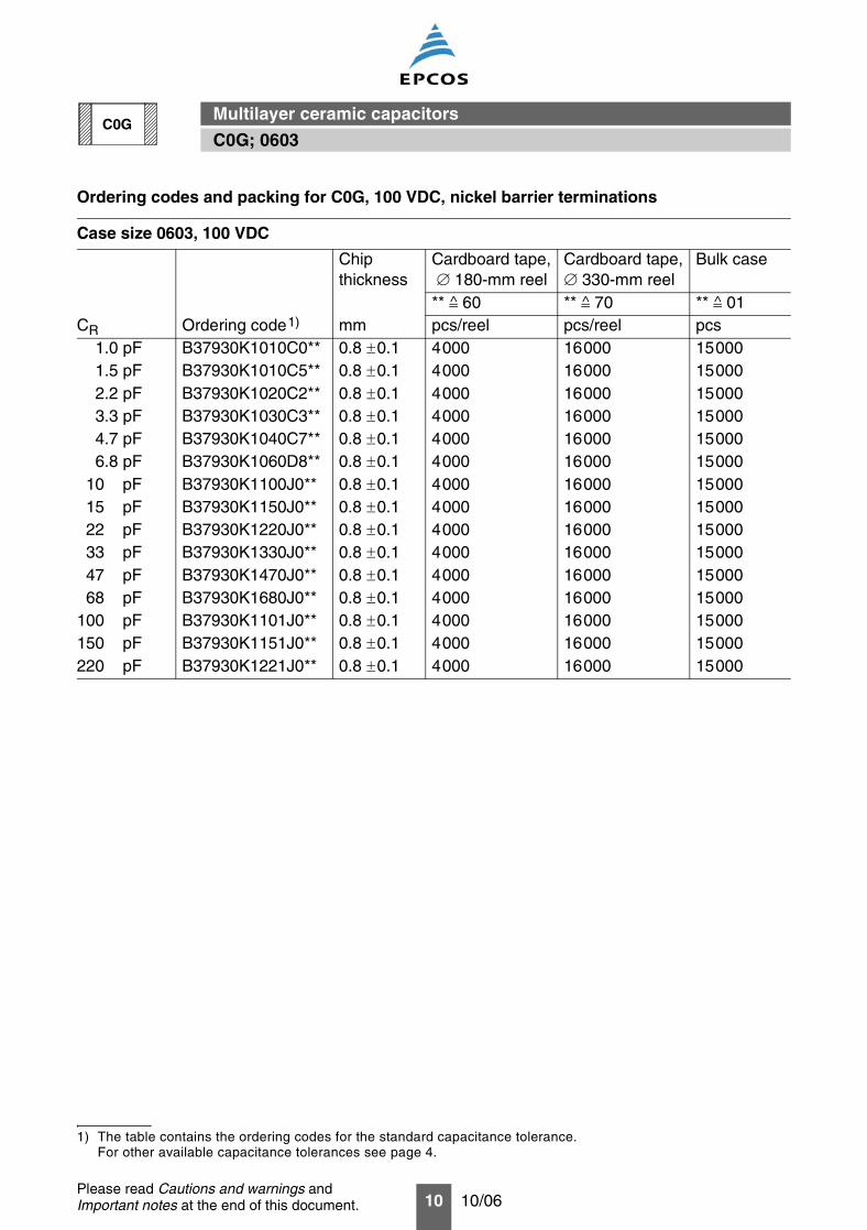
Ordering codes and packing for C0G, 100 VDC, nickel barrier terminations
Case size 0603, 100 VDC
Chipthickness
Cardboard tape, 180-mm reel
Cardboard tape, 330-mm reel
Bulk case
** 60 ** 70 ** 01CR Ordering code1) mm pcs/reel pcs/reel pcs
1.0 pF B37930K1010C0** 0.8 0.1 4000 16000 150001.5 pF B37930K1010C5** 0.8 0.1 4000 16000 150002.2 pF B37930K1020C2** 0.8 0.1 4000 16000 150003.3 pF B37930K1030C3** 0.8 0.1 4000 16000 150004.7 pF B37930K1040C7** 0.8 0.1 4000 16000 150006.8 pF B37930K1060D8** 0.8 0.1 4000 16000 15000
10. pF B37930K1100J0** 0.8 0.1 4000 16000 1500015. pF B37930K1150J0** 0.8 0.1 4000 16000 1500022. pF B37930K1220J0** 0.8 0.1 4000 16000 1500033. pF B37930K1330J0** 0.8 0.1 4000 16000 1500047. pF B37930K1470J0** 0.8 0.1 4000 16000 1500068. pF B37930K1680J0** 0.8 0.1 4000 16000 15000
100. pF B37930K1101J0** 0.8 0.1 4000 16000 15000150. pF B37930K1151J0** 0.8 0.1 4000 16000 15000220. pF B37930K1221J0** 0.8 0.1 4000 16000 15000
1) The table contains the ordering codes for the standard capacitance tolerance.For other available capacitance tolerances see page 4.
^ ^ ^
C0G; 0603
Multilayer ceramic capacitors
11 10/06
C0G
Please read Cautions and warnings andImportant notes at the end of this document.
Ordering codes and packing for C0G, 50 VDC, nickel barrier terminations
Case size 0805, 50 VDC
Chipthickness
Cardboard tape, 180-mm reel
Cardboard tape, 330-mm reel
Bulk case
** 60 ** 70 ** 01CR Ordering code1) mm pcs/reel pcs/reel pcs
1.0 pF B37940K5010C0** 0.6 0.1 5000 20000 100001.2 pF B37940K5010C2** 0.6 0.1 5000 20000 100001.5 pF B37940K5010C5** 0.6 0.1 5000 20000 100001.8 pF B37940K5010C8** 0.6 0.1 5000 20000 100002.2 pF B37940K5020C2** 0.6 0.1 5000 20000 100002.7 pF B37940K5020C7** 0.6 0.1 5000 20000 100003.3 pF B37940K5030C3** 0.6 0.1 5000 20000 100003.9 pF B37940K5030C9** 0.6 0.1 5000 20000 100004.7 pF B37940K5040C7** 0.6 0.1 5000 20000 100005.6 pF B37940K5050D6** 0.6 0.1 5000 20000 100006.8 pF B37940K5060D8** 0.6 0.1 5000 20000 100008.2 pF B37940K5080D2** 0.6 0.1 5000 20000 10000
10. pF B37940K5100J0** 0.6 0.1 5000 20000 1000012. pF B37940K5120J0** 0.6 0.1 5000 20000 1000015. pF B37940K5150J0** 0.6 0.1 5000 20000 1000018. pF B37940K5180J0** 0.6 0.1 5000 20000 1000022. pF B37940K5220J0** 0.6 0.1 5000 20000 1000027. pF B37940K5270J0** 0.6 0.1 5000 20000 1000033. pF B37940K5330J0** 0.6 0.1 5000 20000 1000039. pF B37940K5390J0** 0.6 0.1 5000 20000 1000047. pF B37940K5470J0** 0.6 0.1 5000 20000 1000056. pF B37940K5560J0** 0.6 0.1 5000 20000 1000068. pF B37940K5680J0** 0.6 0.1 5000 20000 1000082. pF B37940K5820J0** 0.6 0.1 5000 20000 10000
100. pF B37940K5101J0** 0.6 0.1 5000 20000 10000120. pF B37940K5121J0** 0.6 0.1 5000 20000 10000150. pF B37940K5151J0** 0.6 0.1 5000 20000 10000180. pF B37940K5181J0** 0.6 0.1 5000 20000 10000220. pF B37940K5221J0** 0.6 0.1 5000 20000 10000270. pF B37940K5271J0** 0.6 0.1 5000 20000 10000330. pF B37940K5331J0** 0.6 0.1 5000 20000 10000390. pF B37940K5391J0** 0.6 0.1 5000 20000 10000470. pF B37940K5471J0** 0.6 0.1 5000 20000 10000
1) The table contains the ordering codes for the standard capacitance tolerance.For other available capacitance tolerances see page 4.
^ ^ ^
C0G; 0805
Multilayer ceramic capacitors
12 10/06
C0G
Please read Cautions and warnings andImportant notes at the end of this document.
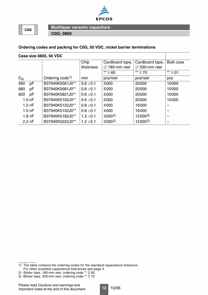
560. pF B37940K5561J0** 0.6 0.1 5000 20000 10000680. pF B37940K5681J0** 0.6 0.1 5000 20000 10000820. pF B37940K5821J0** 0.6 0.1 5000 20000 10000
1.0 nF B37940K5102J0** 0.6 0.1 5000 20000 100001.2 nF B37940K5122J0** 0.8 0.1 4000 16000 –1.5 nF B37940K5152J0** 0.8 0.1 4000 16000 –1.8 nF B37940K5182J0** 1.2 0.1 30002) 120003) –2.2 nF B37940K5222J0** 1.2 0.1 30002) 120003) –
Ordering codes and packing for C0G, 50 VDC, nickel barrier terminations
Case size 0805, 50 VDC
Chipthickness
Cardboard tape, 180-mm reel
Cardboard tape, 330-mm reel
Bulk case
** 60 ** 70 ** 01CR Ordering code1) mm pcs/reel pcs/reel pcs
^ ^ ^
1) The table contains the ordering codes for the standard capacitance tolerance.For other available capacitance tolerances see page 4.
2) Blister tape, 180-mm reel, ordering code ** 623) Blister tape, 330-mm reel, ordering code ** 72
^^
C0G; 0805
Multilayer ceramic capacitors
13 10/06
C0G
Please read Cautions and warnings andImportant notes at the end of this document.
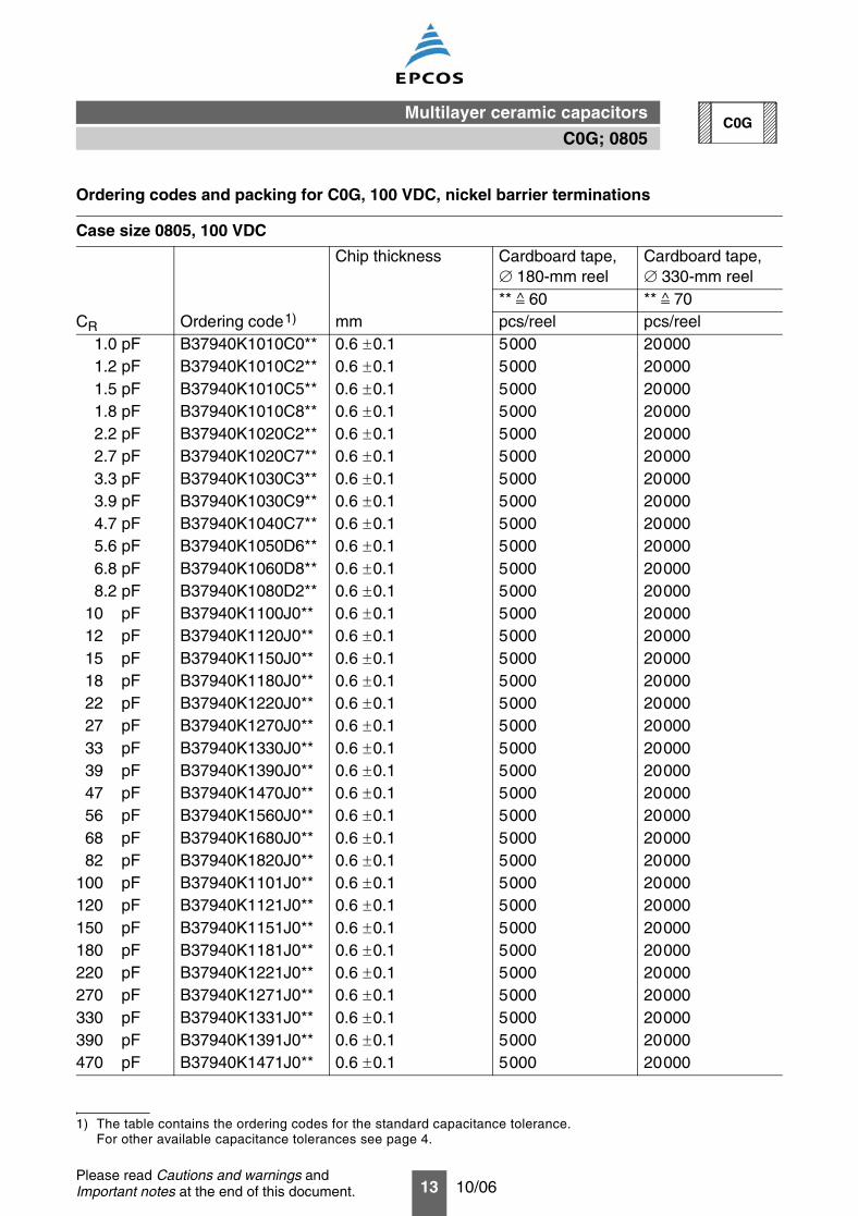
Ordering codes and packing for C0G, 100 VDC, nickel barrier terminations
Case size 0805, 100 VDC
Chip thickness Cardboard tape, 180-mm reel
Cardboard tape, 330-mm reel
** 60 ** 70CR Ordering code1) mm pcs/reel pcs/reel
1.0 pF B37940K1010C0** 0.6 0.1 5000 200001.2 pF B37940K1010C2** 0.6 0.1 5000 200001.5 pF B37940K1010C5** 0.6 0.1 5000 200001.8 pF B37940K1010C8** 0.6 0.1 5000 200002.2 pF B37940K1020C2** 0.6 0.1 5000 200002.7 pF B37940K1020C7** 0.6 0.1 5000 200003.3 pF B37940K1030C3** 0.6 0.1 5000 200003.9 pF B37940K1030C9** 0.6 0.1 5000 200004.7 pF B37940K1040C7** 0.6 0.1 5000 200005.6 pF B37940K1050D6** 0.6 0.1 5000 200006.8 pF B37940K1060D8** 0.6 0.1 5000 200008.2 pF B37940K1080D2** 0.6 0.1 5000 20000
10. pF B37940K1100J0** 0.6 0.1 5000 2000012. pF B37940K1120J0** 0.6 0.1 5000 2000015. pF B37940K1150J0** 0.6 0.1 5000 2000018. pF B37940K1180J0** 0.6 0.1 5000 2000022. pF B37940K1220J0** 0.6 0.1 5000 2000027. pF B37940K1270J0** 0.6 0.1 5000 2000033. pF B37940K1330J0** 0.6 0.1 5000 2000039. pF B37940K1390J0** 0.6 0.1 5000 2000047. pF B37940K1470J0** 0.6 0.1 5000 2000056. pF B37940K1560J0** 0.6 0.1 5000 2000068. pF B37940K1680J0** 0.6 0.1 5000 2000082. pF B37940K1820J0** 0.6 0.1 5000 20000
100. pF B37940K1101J0** 0.6 0.1 5000 20000120. pF B37940K1121J0** 0.6 0.1 5000 20000150. pF B37940K1151J0** 0.6 0.1 5000 20000180. pF B37940K1181J0** 0.6 0.1 5000 20000220. pF B37940K1221J0** 0.6 0.1 5000 20000270. pF B37940K1271J0** 0.6 0.1 5000 20000330. pF B37940K1331J0** 0.6 0.1 5000 20000390. pF B37940K1391J0** 0.6 0.1 5000 20000470. pF B37940K1471J0** 0.6 0.1 5000 20000
1) The table contains the ordering codes for the standard capacitance tolerance.For other available capacitance tolerances see page 4.
^ ^
C0G; 0805
Multilayer ceramic capacitors
14 10/06
C0G
Please read Cautions and warnings andImportant notes at the end of this document.
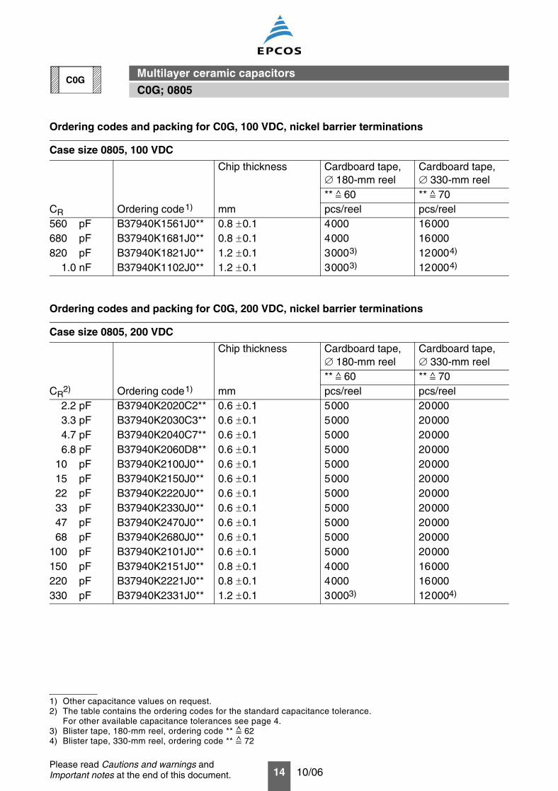
560. pF B37940K1561J0** 0.8 0.1 4000 16000680. pF B37940K1681J0** 0.8 0.1 4000 16000820. pF B37940K1821J0** 1.2 0.1 30003) 120004)
1.0 nF B37940K1102J0** 1.2 0.1 30003) 120004)
Ordering codes and packing for C0G, 200 VDC, nickel barrier terminations
Case size 0805, 200 VDC
Chip thickness Cardboard tape, 180-mm reel
Cardboard tape, 330-mm reel
** 60 ** 70CR
2) Ordering code1) mm pcs/reel pcs/reel2.2 pF B37940K2020C2** 0.6 0.1 5000 200003.3 pF B37940K2030C3** 0.6 0.1 5000 200004.7 pF B37940K2040C7** 0.6 0.1 5000 200006.8 pF B37940K2060D8** 0.6 0.1 5000 20000
10. pF B37940K2100J0** 0.6 0.1 5000 2000015. pF B37940K2150J0** 0.6 0.1 5000 2000022. pF B37940K2220J0** 0.6 0.1 5000 2000033. pF B37940K2330J0** 0.6 0.1 5000 2000047. pF B37940K2470J0** 0.6 0.1 5000 2000068. pF B37940K2680J0** 0.6 0.1 5000 20000
100. pF B37940K2101J0** 0.6 0.1 5000 20000150. pF B37940K2151J0** 0.8 0.1 4000 16000220. pF B37940K2221J0** 0.8 0.1 4000 16000330. pF B37940K2331J0** 1.2 0.1 30003) 120004)
Ordering codes and packing for C0G, 100 VDC, nickel barrier terminations
Case size 0805, 100 VDC
Chip thickness Cardboard tape, 180-mm reel
Cardboard tape, 330-mm reel
** 60 ** 70CR Ordering code1) mm pcs/reel pcs/reel
^ ^
1) Other capacitance values on request.2) The table contains the ordering codes for the standard capacitance tolerance.
For other available capacitance tolerances see page 4.3) Blister tape, 180-mm reel, ordering code ** 624) Blister tape, 330-mm reel, ordering code ** 72
^^
^ ^
C0G; 0805

Multilayer ceramic capacitors
15 10/06
C0G
Please read Cautions and warnings andImportant notes at the end of this document.
Ordering codes and packing for C0G, 50 VDC, nickel barrier terminations
Case size 1206, 50 VDC
Chip thickness Cardboard tape, 180-mm reel
Cardboard tape, 330-mm reel
** 60 ** 70CR Ordering code1) mm pcs/reel pcs/reel
1.0 pF B37871K5010C0** 0.8 0.1 4000 160001.2 pF B37871K5010C2** 0.8 0.1 4000 160001.5 pF B37871K5010C5** 0.8 0.1 4000 160001.8 pF B37871K5010C8** 0.8 0.1 4000 160002.2 pF B37871K5020C2** 0.8 0.1 4000 160002.7 pF B37871K5020C7** 0.8 0.1 4000 160003.3 pF B37871K5030C3** 0.8 0.1 4000 160003.9 pF B37871K5030C9** 0.8 0.1 4000 160004.7 pF B37871K5040C7** 0.8 0.1 4000 160005.6 pF B37871K5050D6** 0.8 0.1 4000 160006.8 pF B37871K5060D8** 0.8 0.1 4000 160008.2 pF B37871K5080D2** 0.8 0.1 4000 16000
10. pF B37871K5100J0** 0.8 0.1 4000 1600012. pF B37871K5120J0** 0.8 0.1 4000 1600015. pF B37871K5150J0** 0.8 0.1 4000 1600018. pF B37871K5180J0** 0.8 0.1 4000 1600022. pF B37871K5220J0** 0.8 0.1 4000 1600027. pF B37871K5270J0** 0.8 0.1 4000 1600033. pF B37871K5330J0** 0.8 0.1 4000 1600039. pF B37871K5390J0** 0.8 0.1 4000 1600047. pF B37871K5470J0** 0.8 0.1 4000 1600056. pF B37871K5560J0** 0.8 0.1 4000 1600068. pF B37871K5680J0** 0.8 0.1 4000 1600082. pF B37871K5820J0** 0.8 0.1 4000 16000
100. pF B37871K5101J0** 0.8 0.1 4000 16000120. pF B37871K5121J0** 0.8 0.1 4000 16000150. pF B37871K5151J0** 0.8 0.1 4000 16000180. pF B37871K5181J0** 0.8 0.1 4000 16000220. pF B37871K5221J0** 0.8 0.1 4000 16000270. pF B37871K5271J0** 0.8 0.1 4000 16000330. pF B37871K5331J0** 0.8 0.1 4000 16000390. pF B37871K5391J0** 0.8 0.1 4000 16000470. pF B37871K5471J0** 0.8 0.1 4000 16000
1) The table contains the ordering codes for the standard capacitance tolerance.For other available capacitance tolerances see page 4.
^ ^
C0G; 1206
Multilayer ceramic capacitors
16 10/06
C0G
Please read Cautions and warnings andImportant notes at the end of this document.
560. pF B37871K5561J0** 0.8 0.1 4000 16000680. pF B37871K5681J0** 0.8 0.1 4000 16000820. pF B37871K5821J0** 0.8 0.1 4000 16000
1.0 nF B37871K5102J0** 0.8 0.1 4000 160001.2 nF B37871K5122J0** 0.8 0.1 4000 160001.5 nF B37871K5152J0** 0.8 0.1 4000 160001.8 nF B37871K5182J0** 0.8 0.1 4000 160002.2 nF B37871K5222J0** 0.8 0.1 4000 160002.7 nF B37871K5272J0** 0.8 0.1 4000 160003.3 nF B37871K5332J0** 0.8 0.1 4000 160003.9 nF B37871K5392J0** 0.8 0.1 4000 160004.7 nF B37871K5472J0** 1.2 0.1 30002) 120003)
5.6 nF B37871K5562J0** 1.2 0.1 30002) 120003)
Ordering codes and packing for C0G, 50 VDC, nickel barrier terminations
Case size 1206, 50 VDC
Chip thickness Cardboard tape, 180-mm reel
Cardboard tape, 330-mm reel
** 60 ** 70CR Ordering code1) mm pcs/reel pcs/reel
^ ^
1) The table contains the ordering codes for the standard capacitance tolerance.For other available capacitance tolerances see page 4.
2) Blister tape, 180-mm reel, ordering code ** 623) Blister tape, 330-mm reel, ordering code ** 72
^^
C0G; 1206
Multilayer ceramic capacitors
17 10/06
C0G
Please read Cautions and warnings andImportant notes at the end of this document.
Ordering codes and packing for C0G, 100 VDC, nickel barrier terminations
Case size 1206, 100 VDC
Chip thickness Cardboard tape, 180-mm reel
Cardboard tape, 330-mm reel
** 60 ** 70CR Ordering code1) mm pcs/reel pcs/reel
1.0 pF B37871K1010C0** 0.8 0.1 4000 160001.5 pF B37871K1010C5** 0.8 0.1 4000 160002.2 pF B37871K1020C2** 0.8 0.1 4000 160003.3 pF B37871K1030C3** 0.8 0.1 4000 160004.7 pF B37871K1040C7** 0.8 0.1 4000 160006.8 pF B37871K1060D8** 0.8 0.1 4000 16000
10. pF B37871K1100J0** 0.8 0.1 4000 1600015. pF B37871K1150J0** 0.8 0.1 4000 1600022. pF B37871K1220J0** 0.8 0.1 4000 1600033. pF B37871K1330J0** 0.8 0.1 4000 1600047. pF B37871K1470J0** 0.8 0.1 4000 1600068. pF B37871K1680J0** 0.8 0.1 4000 16000
100. pF B37871K1101J0** 0.8 0.1 4000 16000150. pF B37871K1151J0** 0.8 0.1 4000 16000220. pF B37871K1221J0** 0.8 0.1 4000 16000330. pF B37871K1331J0** 0.8 0.1 4000 16000470. pF B37871K1471J0** 0.8 0.1 4000 16000680. pF B37871K1681J0** 0.8 0.1 4000 16000
1.0 nF B37871K1102J0** 0.8 0.1 4000 160001.5 nF B37871K1152J0** 0.8 0.1 4000 160002.2 nF B37871K1222J0** 1.2 0.1 30002) 120003)
1) The table contains the ordering codes for the standard capacitance tolerance.For other available capacitance tolerances see page 4.
2) Blister tape, 180-mm reel, ordering code ** 623) Blister tape, 330-mm reel, ordering code ** 72
^^
^ ^
C0G; 1206
Multilayer ceramic capacitors
18 10/06
C0G
Please read Cautions and warnings andImportant notes at the end of this document.
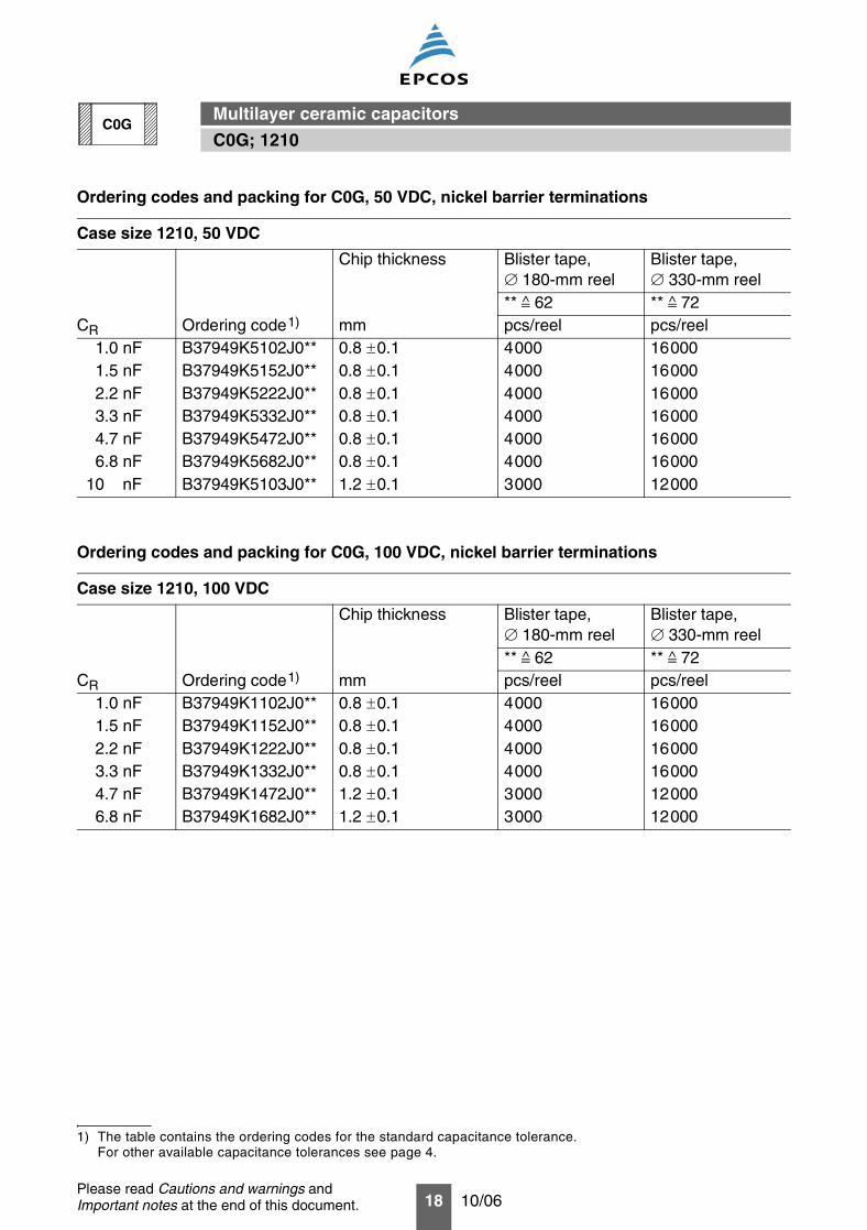
Ordering codes and packing for C0G, 50 VDC, nickel barrier terminations
Case size 1210, 50 VDC
Chip thickness Blister tape, 180-mm reel
Blister tape, 330-mm reel
** 62 ** 72CR Ordering code1) mm pcs/reel pcs/reel
1.0 nF B37949K5102J0** 0.8 0.1 4000 160001.5 nF B37949K5152J0** 0.8 0.1 4000 160002.2 nF B37949K5222J0** 0.8 0.1 4000 160003.3 nF B37949K5332J0** 0.8 0.1 4000 160004.7 nF B37949K5472J0** 0.8 0.1 4000 160006.8 nF B37949K5682J0** 0.8 0.1 4000 16000
10. nF B37949K5103J0** 1.2 0.1 3000 12000
Ordering codes and packing for C0G, 100 VDC, nickel barrier terminations
Case size 1210, 100 VDC
Chip thickness Blister tape, 180-mm reel
Blister tape, 330-mm reel
** 62 ** 72CR Ordering code1) mm pcs/reel pcs/reel
1.0 nF B37949K1102J0** 0.8 0.1 4000 160001.5 nF B37949K1152J0** 0.8 0.1 4000 160002.2 nF B37949K1222J0** 0.8 0.1 4000 160003.3 nF B37949K1332J0** 0.8 0.1 4000 160004.7 nF B37949K1472J0** 1.2 0.1 3000 120006.8 nF B37949K1682J0** 1.2 0.1 3000 12000
1) The table contains the ordering codes for the standard capacitance tolerance.For other available capacitance tolerances see page 4.
^ ^
^ ^
C0G; 1210
Multilayer ceramic capacitors
19 10/06
C0G
Please read Cautions and warnings andImportant notes at the end of this document.
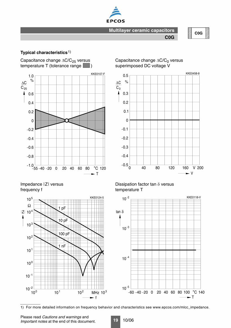
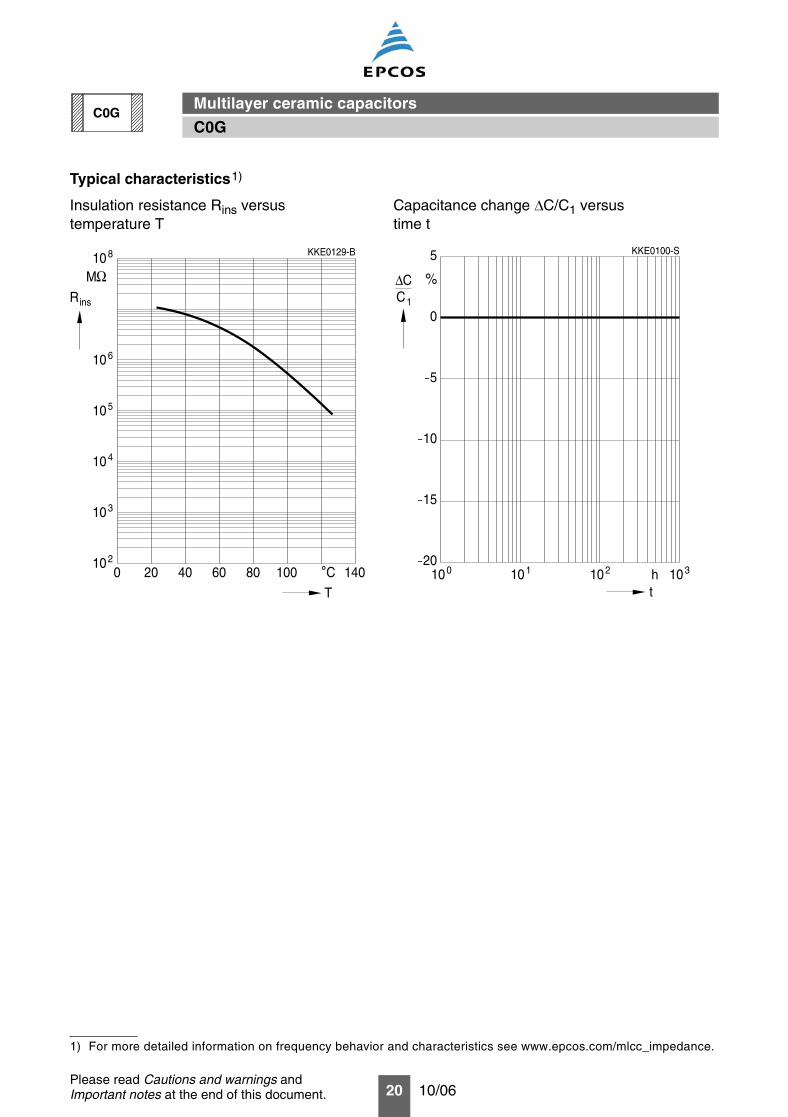
Typical characteristics1)
Capacitance change C/C25 versustemperature T (tolerance range )
Capacitance change C/C0 versussuperimposed DC voltage V
Impedance |Z| versusfrequency f
Dissipation factor tan versustemperature T
1) For more detailed information on frequency behavior and characteristics see www.epcos.com/mlcc_impedance.
KKE0107-F
25
T0 20 40 60 80 120
0
0.2
0.4
0.6
1.0%
C∆C
55_ _40 20__1.0
0.8_
0.6_
0.4_
0.2_
C˚
KKE0458-8
0
V80 120 160 V 200
0
0.1
0.2
0.3
0.5
%C∆C
400
0.1_
_0.2
_0.3
_0.4
_0.5
KKE0124-5
100 101 102 103
Z
10
f
2_
MHz
10_1
100
110
102
103
104
510
Ω1 pF
10 pF
100 pF
1 nF
KKE0118-V
tan
T0 20 40 60 80 100 140
δ
60_ 40_ 20_510
_
10 4_
10 3_
10 2_
C˚
C0G
Multilayer ceramic capacitors
20 10/06
C0G
Please read Cautions and warnings andImportant notes at the end of this document.
Typical characteristics1)
Insulation resistance Rins versustemperature T
Capacitance change C/C1 versustime t
1) For more detailed information on frequency behavior and characteristics see www.epcos.com/mlcc_impedance.
KKE0129-B
R
T
210
ins
0 20 40 60 80 100 140
103
104
105
106
108
MΩ
C˚
KKE0100-S
th100 101 102 103
C∆C1
_10
15
20_
_
_5
0
%
5
C0G
21 10/06
Multilayer ceramic capacitors
Cautions and warnings
Notes on the selection of ceramic capacitors
In the selection of ceramic capacitors, the following criteria must be considered:
1. Depending on the application, ceramic capacitors used to meet high quality requirements shouldat least satisfy the specifications to AEC-Q200. They must meet quality requirements goingbeyond this level in terms of ruggedness (e.g. mechanical, thermal or electrical) in the case ofcritical circuit configurations and applications (e.g. in safety-relevant applications such as ABSand airbag equipment or durable industrial goods).
2. At the connection to the battery or power supply (e.g. clamp 15 or 30 in the automobile) and atpositions with stranding potential, to reduce the probability of short circuits following a fracture,two ceramic capacitors must be connected in series and/or a ceramic capacitor with integratedseries circuit should be used. The MLSC from EPCOS contains such a series circuit in a singlecomponent.
3. Ceramic capacitors with the temperature characteristics Z5U and Y5V do not satisfy the require-ments to AEC-Q200 and are mechanically and electrically less rugged than C0G or X7R/X8Rceramic capacitors. In applications that must satisfy high quality requirements, therefore, thesecapacitors should not be used as discrete components (see the chapter “Effects on mechanical,thermal and electrical stress”, point 1.4).
4. For ESD protection, preference should be given to the use of multilayer varistors (MLV) (see thechapter “Effects on mechanical, thermal and electrical stress”, point 1.4).
5. An application-specific derating or continuous operating voltage must be considered in order tocushion (unexpected) additional stresses (see the chapter “Reliability”).
The following should be considered in circuit board design
1. If technically feasible in the application, preference should be given to components having anoptimal geometrical design.
2. At least FR4 circuit board material should be used.
3. Geometrically optimal circuit boards should be used, ideally those that cannot be deformed.
4. Ceramic capacitors must always be placed a sufficient minimum distance from the edge of thecircuit board. High bending forces may be exerted there when the panels are separated and dur-ing further processing of the board (such as when incorporating it into a housing).
5. Ceramic capacitors should always be placed parallel to the possible bending axis of the circuitboard.
6. No screw connections should be used to fix the board or to connect several boards. Compo-nents should not be placed near screw holes. If screw connections are unavoidable, they mustbe cushioned (for instance by rubber pads).
22 10/06
Multilayer ceramic capacitors
Cautions and warnings
The following should be considered in the placement process
1. Ensure correct positioning of the ceramic capacitor on the solder pad.
2. Caution when using casting, injection-molded and molding compounds and cleaning agents,as these may damage the capacitor.
3. Support the circuit board and reduce the placement forces.
4. A board should not be straightened (manually) if it has been distorted by soldering.
5. Separate panels with a peripheral saw, or better with a milling head (no dicing or breaking).
6. Caution in the subsequent placement of heavy or leaded components (e.g. transformers orsnap-in components): danger of bending and fracture.
7. When testing, transporting, packing or incorporating the board, avoid any deformation of theboard not to damage the components.
8. Avoid the use of excessive force when plugging a connector into a device soldered onto theboard.
9. Ceramic capacitors must be soldered only by the mode (reflow or wave soldering) permissiblefor them (see the chapter “Soldering directions”).
10. When soldering the most gentle solder profile feasible should be selected (heating time, peaktemperature, cooling time) in order to avoid thermal stresses and damage.
11. Ensure the correct solder meniscus height and solder quantity.
12. Ensure correct dosing of the cement quantity.
13. Ceramic capacitors with an AgPd external termination are not suited for the lead-free solderprocess: they were developed only for conductive adhesion technology.
This listing does not claim to be complete, but merely reflects the experience of EPCOS AG.
23 10/06
Multilayer ceramic capacitors
Important notes
The following applies to all products named in this publication:
1. Some parts of this publication contain statements about the suitability of our products forcertain areas of application. These statements are based on our knowledge of typicalrequirements that are often placed on our products in the areas of application concerned. Wenevertheless expressly point out that such statements cannot be regarded as bindingstatements about the suitability of our products for a particular customer application. Asa rule, EPCOS is either unfamiliar with individual customer applications or less familiar with themthan the customers themselves. For these reasons, it is always ultimately incumbent on thecustomer to check and decide whether an EPCOS product with the properties described in theproduct specification is suitable for use in a particular customer application.
2. We also point out that in individual cases, a malfunction of passive electronic componentsor failure before the end of their usual service life cannot be completely ruled out in thecurrent state of the art, even if they are operated as specified. In customer applicationsrequiring a very high level of operational safety and especially in customer applications in whichthe malfunction or failure of a passive electronic component could endanger human life or health(e.g. in accident prevention or life-saving systems), it must therefore be ensured by means ofsuitable design of the customer application or other action taken by the customer (e.g.installation of protective circuitry or redundancy) that no injury or damage is sustained by thirdparties in the event of malfunction or failure of a passive electronic component.
3. The warnings, cautions and product-specific notes must be observed.
4. In order to satisfy certain technical requirements, some of the products described in thispublication may contain substances subject to restrictions in certain jurisdictions (e.g.because they are classed as “hazardous”). Useful information on this will be found in ourMaterial Data Sheets on the Internet (www.epcos.com/material). Should you have any moredetailed questions, please contact our sales offices.
5. We constantly strive to improve our products. Consequently, the products described in thispublication may change from time to time. The same is true of the corresponding productspecifications. Please check therefore to what extent product descriptions and specificationscontained in this publication are still applicable before or when you place an order.
We also reserve the right to discontinue production and delivery of products.Consequently, we cannot guarantee that all products named in this publication will always beavailable.
6. Unless otherwise agreed in individual contracts, all orders are subject to the current versionof the “General Terms of Delivery for Products and Services in the Electrical Industry”published by the German Electrical and Electronics Industry Association (ZVEI).
7. The trade names EPCOS, EPCOS-JONES, Baoke, CeraDiode, CSSP, MLSC, PhaseCap,PhaseMod, SIFERRIT, SIFI, SIKOREL, SilverCap, SIMID, SIOV, SIP5D, SIP5K, UltraCap,WindCap are trademarks registered or pending in Europe and in other countries. Furtherinformation will be found on the Internet at www.epcos.com/trademarks.