Embed Size (px)
Citation preview
Indust r ia l Power
2ED100E12-F2_EVAL
6ED100E12-F2_EVAL E v a l u a t i o n D r i v e r B o a r d f o r E c o n o D U A L ™ 3 a n d E c o n o P A C K ™ + m o d u l e s
App l i ca t i on No te , V1 .2 , Aug . 2009
AN2008-02
Edition 2009-11-02 Published by Infineon Technologies AG 59568 Warstein, Germany © Infineon Technologies AG 2009. All Rights Reserved.
LEGAL DISCLAIMER THE INFORMATION GIVEN IN THIS APPLICATION NOTE IS GIVEN AS A HINT FOR THE IMPLEMENTATION OF THE INFINEON TECHNOLOGIES COMPONENT ONLY AND SHALL NOT BE REGARDED AS ANY DESCRIPTION OR WARRANTY OF A CERTAIN FUNCTIONALITY, CONDITION OR QUALITY OF THE INFINEON TECHNOLOGIES COMPONENT. THE RECIPIENT OF THIS APPLICATION NOTE MUST VERIFY ANY FUNCTION DESCRIBED HEREIN IN THE REAL APPLICATION. INFINEON TECHNOLOGIES HEREBY DISCLAIMS ANY AND ALL WARRANTIES AND LIABILITIES OF ANY KIND (INCLUDING WITHOUT LIMITATION WARRANTIES OF NON-INFRINGEMENT OF INTELLECTUAL PROPERTY RIGHTS OF ANY THIRD PARTY) WITH RESPECT TO ANY AND ALL INFORMATION GIVEN IN THIS APPLICATION NOTE.
Information For further information on technology, delivery terms and conditions and prices please contact your nearest Infineon Technologies Office (www.infineon.com).
Warnings Due to technical requirements components may contain dangerous substances. For information on the types in question please contact your nearest Infineon Technologies Office. Infineon Technologies Components may only be used in life-support devices or systems with the express written approval of Infineon Technologies, if a failure of such components can reasonably be expected to cause the failure of that life-support device or system, or to affect the safety or effectiveness of that device or system. Life support devices or systems are intended to be implanted in the human body, or to support and/or maintain and sustain and/or protect human life. If they fail, it is reasonable to assume that the health of the user or other persons may be endangered.
AN2008-02 Driver board for EconoDUAL™3 and EconoPACK™+
Application Note 3 V1.2, 2009-08
AN2008-02 Revision History: 2009-08 V1.2 Previous Version: V1.1 general Improved driver stage for higher gate current to adapt for IGBT4 (2ED100E12-F2) general Improved protection against disturbances on DESAT-signal (2ED100E12-F2) general Providing data for increased portofolio of modules to be used with 2ED100E12-F2 general Update of measurement results (modules using IGBT4) Page 7 Update with recent data from 1ED020I12-F datasheet Page 16 More detailed text on baseplate temperature measurement Page 17 Discussing parameters having impact on switching losses Page 40 References
Authors: Alain Siani IFAG IMM INP TM, Uwe Jansen IFAG IMM INP TM
We Listen to Your Comments Any information within this document that you feel is wrong, unclear or missing at all? Your feedback will help us to continuously improve the quality of this document. Please send your proposal (including a reference to this document) to: [email protected]
AN2008-02 Driver board for EconoDUAL™3 and EconoPACK™+
Introduction
Application Note 4 V1.2, 2009-08
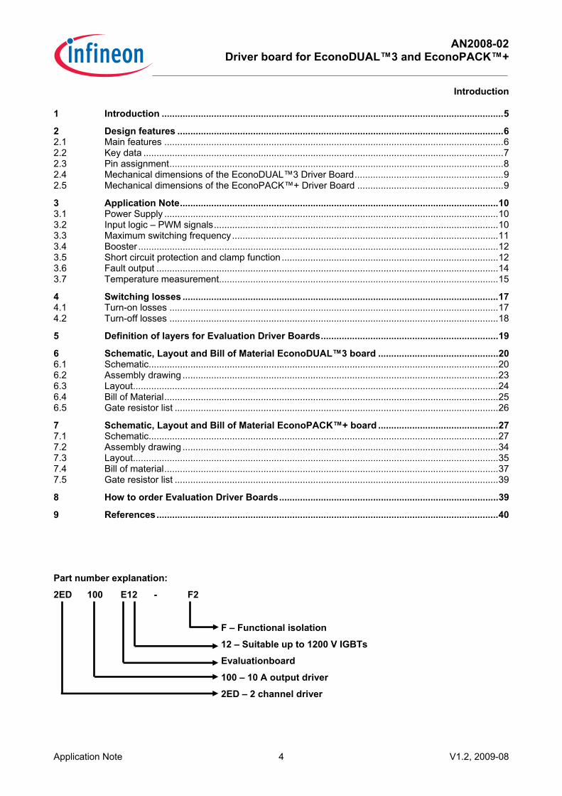
1 Introduction ...................................................................................................................................5 2 Design features .............................................................................................................................6 2.1 Main features ..................................................................................................................................6 2.2 Key data ..........................................................................................................................................7 2.3 Pin assignment................................................................................................................................8 2.4 Mechanical dimensions of the EconoDUAL™3 Driver Board.........................................................9 2.5 Mechanical dimensions of the EconoPACK™+ Driver Board ........................................................9 3 Application Note..........................................................................................................................10 3.1 Power Supply ................................................................................................................................10 3.2 Input logic – PWM signals.............................................................................................................10 3.3 Maximum switching frequency......................................................................................................11 3.4 Booster ..........................................................................................................................................12 3.5 Short circuit protection and clamp function ...................................................................................12 3.6 Fault output ...................................................................................................................................14 3.7 Temperature measurement...........................................................................................................15 4 Switching losses .........................................................................................................................17 4.1 Turn-on losses ..............................................................................................................................17 4.2 Turn-off losses ..............................................................................................................................18 5 Definition of layers for Evaluation Driver Boards....................................................................19 6 Schematic, Layout and Bill of Material EconoDUAL™3 board ..............................................20 6.1 Schematic......................................................................................................................................20 6.2 Assembly drawing .........................................................................................................................23 6.3 Layout............................................................................................................................................24 6.4 Bill of Material................................................................................................................................25 6.5 Gate resistor list ............................................................................................................................26 7 Schematic, Layout and Bill of Material EconoPACK™+ board ..............................................27 7.1 Schematic......................................................................................................................................27 7.2 Assembly drawing .........................................................................................................................34 7.3 Layout............................................................................................................................................35 7.4 Bill of material................................................................................................................................37 7.5 Gate resistor list ............................................................................................................................39 8 How to order Evaluation Driver Boards....................................................................................39 9 References...................................................................................................................................40
Part number explanation:
2ED 100 E12 - F2
F – Functional isolation
12 – Suitable up to 1200 V IGBTs
Evaluationboard
100 – 10 A output driver
2ED – 2 channel driver
AN2008-02 Driver board for EconoDUAL™3 and EconoPACK™+
Introduction
Application Note 5 V1.2, 2009-08
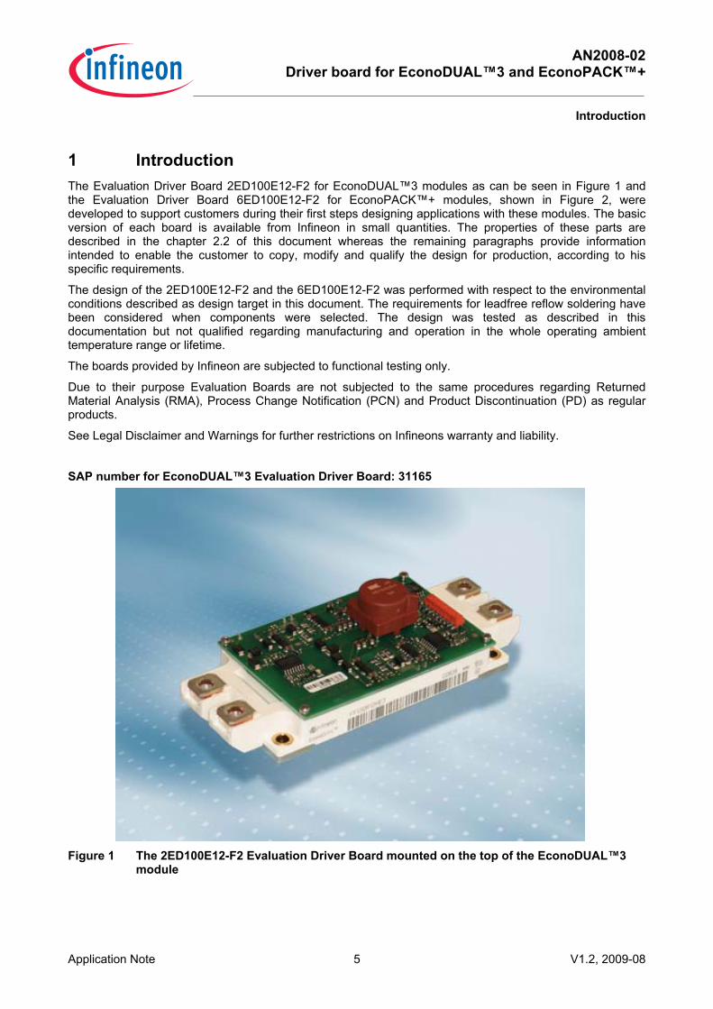
1 Introduction The Evaluation Driver Board 2ED100E12-F2 for EconoDUAL™3 modules as can be seen in Figure 1 and the Evaluation Driver Board 6ED100E12-F2 for EconoPACK™+ modules, shown in Figure 2, were developed to support customers during their first steps designing applications with these modules. The basic version of each board is available from Infineon in small quantities. The properties of these parts are described in the chapter 2.2 of this document whereas the remaining paragraphs provide information intended to enable the customer to copy, modify and qualify the design for production, according to his specific requirements.
The design of the 2ED100E12-F2 and the 6ED100E12-F2 was performed with respect to the environmental conditions described as design target in this document. The requirements for leadfree reflow soldering have been considered when components were selected. The design was tested as described in this documentation but not qualified regarding manufacturing and operation in the whole operating ambient temperature range or lifetime.
The boards provided by Infineon are subjected to functional testing only.
Due to their purpose Evaluation Boards are not subjected to the same procedures regarding Returned Material Analysis (RMA), Process Change Notification (PCN) and Product Discontinuation (PD) as regular products.
See Legal Disclaimer and Warnings for further restrictions on Infineons warranty and liability.
SAP number for EconoDUAL™3 Evaluation Driver Board: 31165
Figure 1 The 2ED100E12-F2 Evaluation Driver Board mounted on the top of the EconoDUAL™3
module
AN2008-02 Driver board for EconoDUAL™3 and EconoPACK™+
Design features
Application Note 6 V1.2, 2009-08
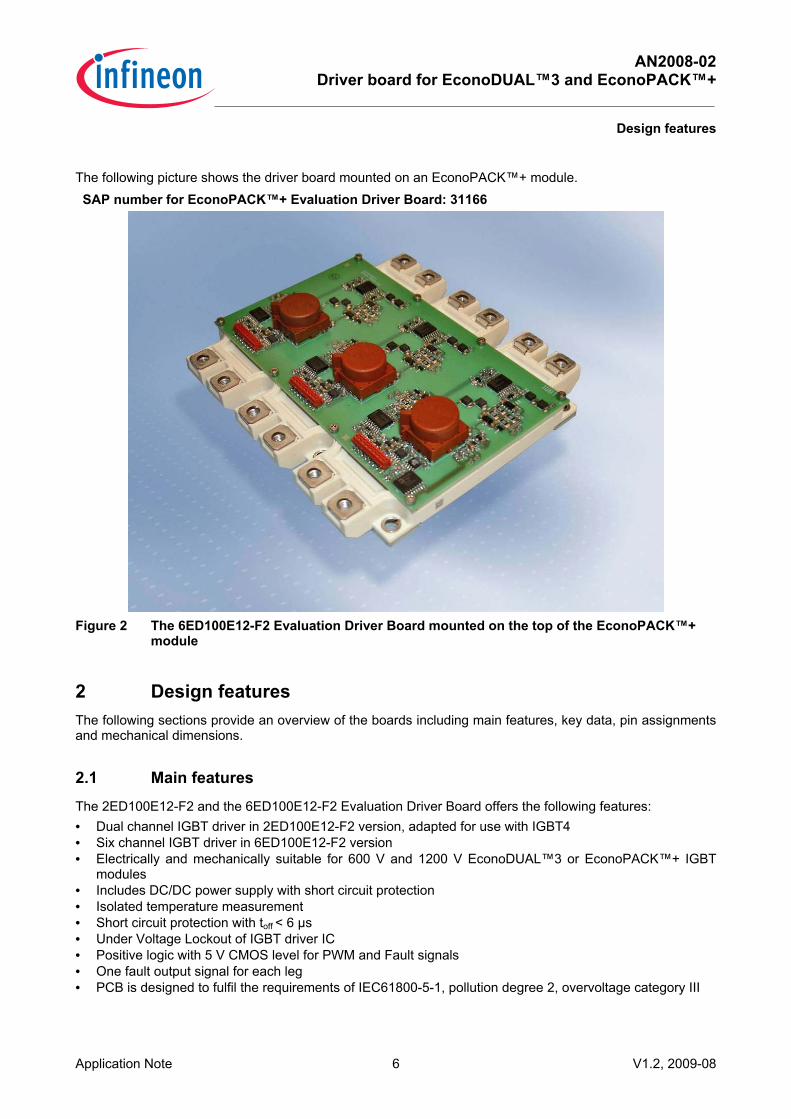
The following picture shows the driver board mounted on an EconoPACK™+ module. SAP number for EconoPACK™+ Evaluation Driver Board: 31166
Figure 2 The 6ED100E12-F2 Evaluation Driver Board mounted on the top of the EconoPACK™+
module
2 Design features The following sections provide an overview of the boards including main features, key data, pin assignments and mechanical dimensions.
2.1 Main features
The 2ED100E12-F2 and the 6ED100E12-F2 Evaluation Driver Board offers the following features: • Dual channel IGBT driver in 2ED100E12-F2 version, adapted for use with IGBT4 • Six channel IGBT driver in 6ED100E12-F2 version • Electrically and mechanically suitable for 600 V and 1200 V EconoDUAL™3 or EconoPACK™+ IGBT
modules • Includes DC/DC power supply with short circuit protection • Isolated temperature measurement • Short circuit protection with toff < 6 µs • Under Voltage Lockout of IGBT driver IC • Positive logic with 5 V CMOS level for PWM and Fault signals • One fault output signal for each leg • PCB is designed to fulfil the requirements of IEC61800-5-1, pollution degree 2, overvoltage category III
AN2008-02 Driver board for EconoDUAL™3 and EconoPACK™+
Design features
Application Note 7 V1.2, 2009-08
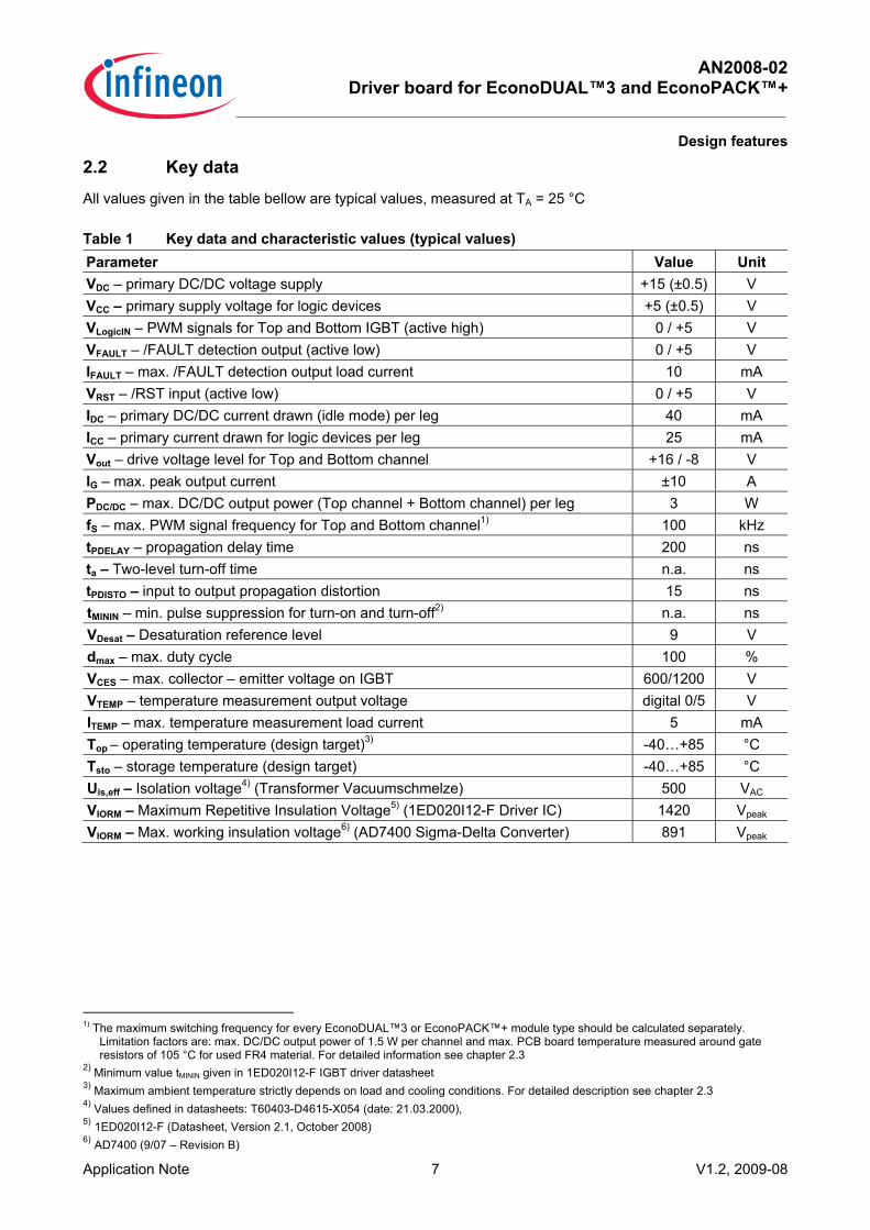
2.2 Key data
All values given in the table bellow are typical values, measured at TA = 25 °C
Table 1 Key data and characteristic values (typical values) Parameter Value Unit VDC – primary DC/DC voltage supply +15 (±0.5) V VCC – primary supply voltage for logic devices +5 (±0.5) V VLogicIN – PWM signals for Top and Bottom IGBT (active high) 0 / +5 V VFAULT – /FAULT detection output (active low) 0 / +5 V IFAULT – max. /FAULT detection output load current 10 mA VRST – /RST input (active low) 0 / +5 V IDC – primary DC/DC current drawn (idle mode) per leg 40 mA ICC – primary current drawn for logic devices per leg 25 mA Vout – drive voltage level for Top and Bottom channel +16 / -8 V IG – max. peak output current ±10 A PDC/DC – max. DC/DC output power (Top channel + Bottom channel) per leg 3 W fS – max. PWM signal frequency for Top and Bottom channel1) 100 kHz tPDELAY – propagation delay time 200 ns ta – Two-level turn-off time n.a. ns tPDISTO – input to output propagation distortion 15 ns tMININ – min. pulse suppression for turn-on and turn-off2) n.a. ns VDesat – Desaturation reference level 9 V dmax – max. duty cycle 100 % VCES – max. collector – emitter voltage on IGBT 600/1200 V VTEMP – temperature measurement output voltage digital 0/5 V ITEMP – max. temperature measurement load current 5 mA Top – operating temperature (design target)3) -40…+85 °C Tsto – storage temperature (design target) -40…+85 °C Uis,eff – Isolation voltage4) (Transformer Vacuumschmelze) 500 VAC VIORM – Maximum Repetitive Insulation Voltage5) (1ED020I12-F Driver IC) 1420 Vpeak
VIORM – Max. working insulation voltage6) (AD7400 Sigma-Delta Converter) 891 Vpeak
1) The maximum switching frequency for every EconoDUAL™3 or EconoPACK™+ module type should be calculated separately.
Limitation factors are: max. DC/DC output power of 1.5 W per channel and max. PCB board temperature measured around gate resistors of 105 °C for used FR4 material. For detailed information see chapter 2.3
2) Minimum value tMININ given in 1ED020I12-F IGBT driver datasheet 3) Maximum ambient temperature strictly depends on load and cooling conditions. For detailed description see chapter 2.3 4) Values defined in datasheets: T60403-D4615-X054 (date: 21.03.2000), 5) 1ED020I12-F (Datasheet, Version 2.1, October 2008) 6) AD7400 (9/07 – Revision B)
AN2008-02 Driver board for EconoDUAL™3 and EconoPACK™+
Design features
Application Note 8 V1.2, 2009-08
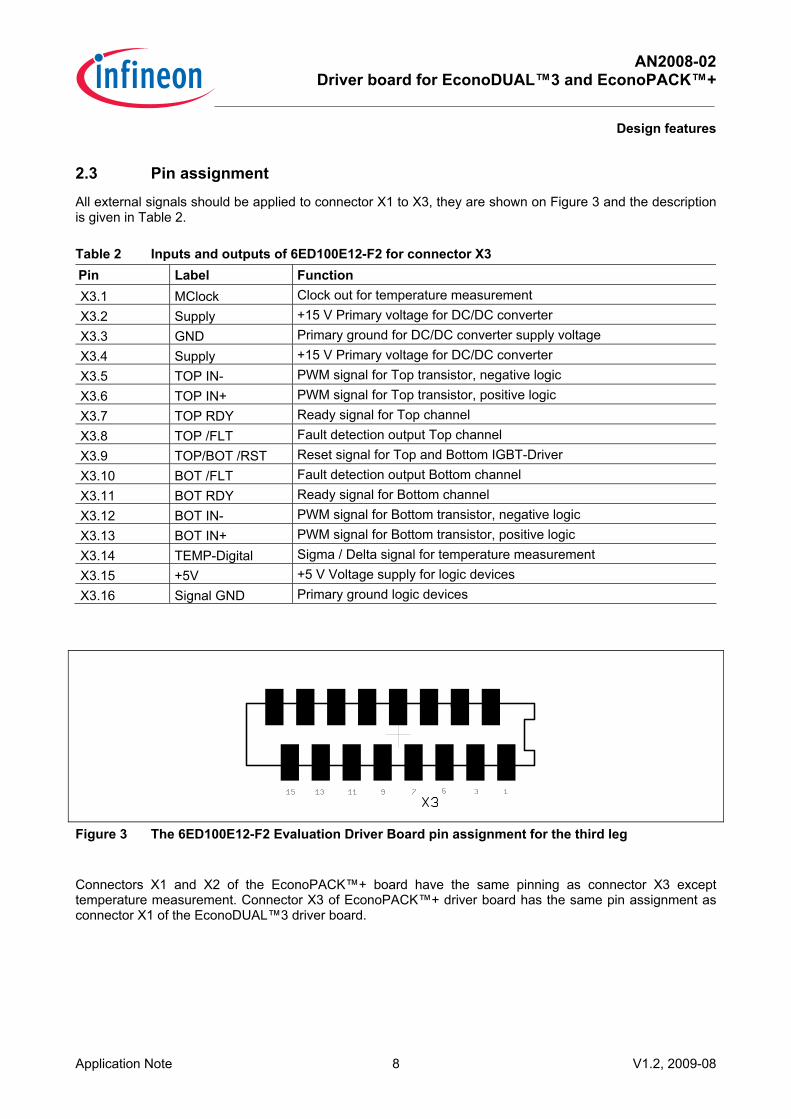
2.3 Pin assignment
All external signals should be applied to connector X1 to X3, they are shown on Figure 3 and the description is given in Table 2.
Table 2 Inputs and outputs of 6ED100E12-F2 for connector X3 Pin Label Function X3.1 MClock Clock out for temperature measurement X3.2 Supply +15 V Primary voltage for DC/DC converter X3.3 GND Primary ground for DC/DC converter supply voltage X3.4 Supply +15 V Primary voltage for DC/DC converter X3.5 TOP IN- PWM signal for Top transistor, negative logic X3.6 TOP IN+ PWM signal for Top transistor, positive logic X3.7 TOP RDY Ready signal for Top channel X3.8 TOP /FLT Fault detection output Top channel X3.9 TOP/BOT /RST Reset signal for Top and Bottom IGBT-Driver X3.10 BOT /FLT Fault detection output Bottom channel X3.11 BOT RDY Ready signal for Bottom channel X3.12 BOT IN- PWM signal for Bottom transistor, negative logic X3.13 BOT IN+ PWM signal for Bottom transistor, positive logic X3.14 TEMP-Digital Sigma / Delta signal for temperature measurement X3.15 +5V +5 V Voltage supply for logic devices X3.16 Signal GND Primary ground logic devices
Figure 3 The 6ED100E12-F2 Evaluation Driver Board pin assignment for the third leg
Connectors X1 and X2 of the EconoPACK™+ board have the same pinning as connector X3 except temperature measurement. Connector X3 of EconoPACK™+ driver board has the same pin assignment as connector X1 of the EconoDUAL™3 driver board.
AN2008-02 Driver board for EconoDUAL™3 and EconoPACK™+
Design features
Application Note 9 V1.2, 2009-08
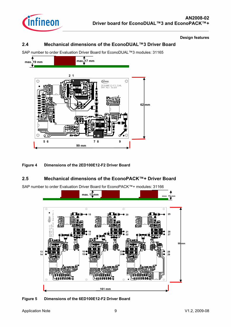
2.4 Mechanical dimensions of the EconoDUAL™3 Driver Board SAP number to order Evaluation Driver Board for EconoDUAL™3 modules: 31165
Figure 4 Dimensions of the 2ED100E12-F2 Driver Board
2.5 Mechanical dimensions of the EconoPACK™+ Driver Board
Figure 5 Dimensions of the 6ED100E12-F2 Driver Board
SAP number to order Evaluation Driver Board for EconoPACK™+ modules: 31166
99 mm
62 mm
2 1
9 7 8 5 6
max. 17 mm max. 19 mm
161 mm
max. 17 mm max. 19 mm
99 mm
13 14
25
26 27
28 29
2122
2324
16 17
18 19
15 20
X X X
AN2008-02 Driver board for EconoDUAL™3 and EconoPACK™+
Application Note
Application Note 10 V1.2, 2009-08
Both Driver Boards should be fastened by self taping screws and soldered to the auxiliary connectors on top of the IGBT module.
Clearance and creepage distances for EconoDUAL™3 and EconoPACK™+ Driver Boards:
Primary/Secondary is not less than 8 mm and Secondary/Secondary is not less than 4 mm.
3 Application Note The following chapter describes the board´s operation in evaluation setup. Please note that the following paragraphs describe the circuits of the 2ED100E12-F2 which has been modified (compared to the last revision of this AN) to drive IGBT4 modules and to reduce the susceptibility to erroneous triggering of the Vcesat-detection. Same changes may also be applied to the 6ED100E12-12-F2, but layout and part list of this board provided in chapter 7 still represent the initial design.
3.1 Power Supply
The 2ED100E12-F2 and the 6ED100E12-F2 have an integrated DC/DC converter for each leg, which generates the required secondary isolated unsymmetrical supply voltage of +16 V / -8 V. Top and Bottom driver voltages are independently generated by using one unipolar input voltage of 15 V. Additionally, the power supply is protected against gate – emitter short circuit of the IGBTs. In case of DC/DC converter overload, the output voltage drops. This Under Voltage Detection function insures gate voltages within specified range. The fault is reported to the driver’s primary side.
3.2 Input logic – PWM signals
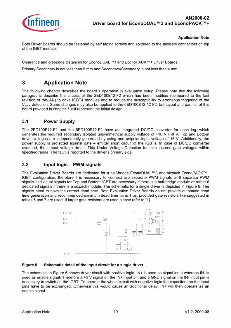
The Evaluation Driver Boards are dedicated for a half-bridge EconoDUAL™3 and sixpack EconoPACK™+ IGBT configuration, therefore it is necessary to connect two separate PWM signals or 6 separate PWM signals. Individual signals for Top and Bottom IGBT are necessary if there is a half-bridge module or rather 6 dedicated signals if there is a sixpack module. The schematic for a single driver is depicted in Figure 6. The signals need to have the correct dead time. Both Evaluation Driver Boards do not provide automatic dead time generation and recommended minimum dead time tTD is 1 µs, provided gate resistors like suggested in tables 5 and 7 are used. If larger gate resistors are used please refer to [1].
Figure 6 Schematic detail of the input circuit for a single driver.
The schematic in Figure 6 shows driver circuit with positive logic. IN+ is used as signal input whereas IN- is used as enable signal. Therefore a +5 V signal on the IN+ input pin and a GND signal on the IN- input pin is necessary to switch on the IGBT. To operate the whole circuit with negative logic the capacitors on the input pins have to be exchanged. Otherwise this would cause an additional delay. IN+ will then operate as an enable signal.
AN2008-02 Driver board for EconoDUAL™3 and EconoPACK™+
Application Note
Application Note 11 V1.2, 2009-08
3.3 Maximum switching frequency
The IGBT switching frequency is limited by the available power and by PCB temperature. According to theory the power losses generated in gate resistors are a function of gate charge, voltage step at the driver output and switching frequency. The energy is dissipated mainly through the PCB and raises the temperature around the gate resistors. When the available power of the DC/DC converter is not exceeded, the limiting factor for the switching frequency is the absolute maximum temperature for the FR4 material. The allowed operation temperature is 105 °C.
Generally the power losses generated in the gate resistors can be calculated according to formula (1):
gesoutRgRgextdis QfVPPP ⋅⋅∆=+= int (1)
In this formula sf resembles the switching frequency, outV∆ represents the voltage step at the driver output
disP is the dissipated power, geQ is the IGBT gate charge value corresponding to -8/+16V operation. This value can be approximately calculated from the datasheet value by multiplying by 0.8.
Most of the losses are shared between the internal – intRgP and the external – RgextP gate resistors.
Negligible losses are also in the driver IC itself. Due to the PCB temperature criteria the power dissipated in external gate resistors gextRP is to be considerd for the thermal design. Temperatures can be calculated takeing relevant thermal resistances of this part of the board into account.
Based on experimentally determined board temperatures the following thermal resistances have been calculated using an equivalent circuit diagram as given in Figure 7:
Gate resistors to baseplate: RthB-G = 45 K/W
Gate resistors to ambient: RthR-A = 39 K/W
Figure 7 Thermal equivalent circuit
TA
TBASE
TG
RthR-A
RthB-G
PCB
AIR
RthB-G
RthR-A
PRgext PRgext
GthBAthR
ABASEGthB
RRTTR
−−
−
+− )(*
IGBT
AN2008-02 Driver board for EconoDUAL™3 and EconoPACK™+
Application Note
Application Note 12 V1.2, 2009-08
Using these values and the equivalent circuit, it is possible to determine the maximum board temperature, if the power losses of the external gate resistors, the maximum ambient temperature and the maximum baseplate temperature are known:
GthBAthR
GthBAthRRgext
GthBAthR
ABASEGthBAG RR
RRPRR
TTRTT−−
−−
−−
−
++
+−+= **)(*
The maximum switching frequency will be determined when either the maximum allowable board temperature has been reached (105°C) or when the limit of power transmission of the DC/DC converter (1.5 W per channel) is exceeded.
3.4 Booster
Two complementary pairs of transistors are used to amplify the driver ICs signal. This allows driving IGBTs that need more current than the driver IC can deliver. Two NPN transistors are used for switching the IGBT on and two PNP transistors for switching the IGBT off. Resistors in the individual base connections ensure proper parallel operation.
The transistors are dimensioned to have enough peak current to drive all 600 V and 1200 V EconoDUAL™3 and EconoPACK™+ modules. Peak current can be calculated like in formula (2):
DriverGG
outpeak RRR
VIext
++∆=
int
(2)
Figure 8 Booster
Gate resistors are connected in between booster stage and IGBT module gate connection. Suggested values are provided in tables 5 and 7. For some modules the value for these resistors is 0 Ohm. In this case just a jumper is required. If resistors are needed ensure that these resistors have a suitable rating for repetitive pulse power to avoid degradation.
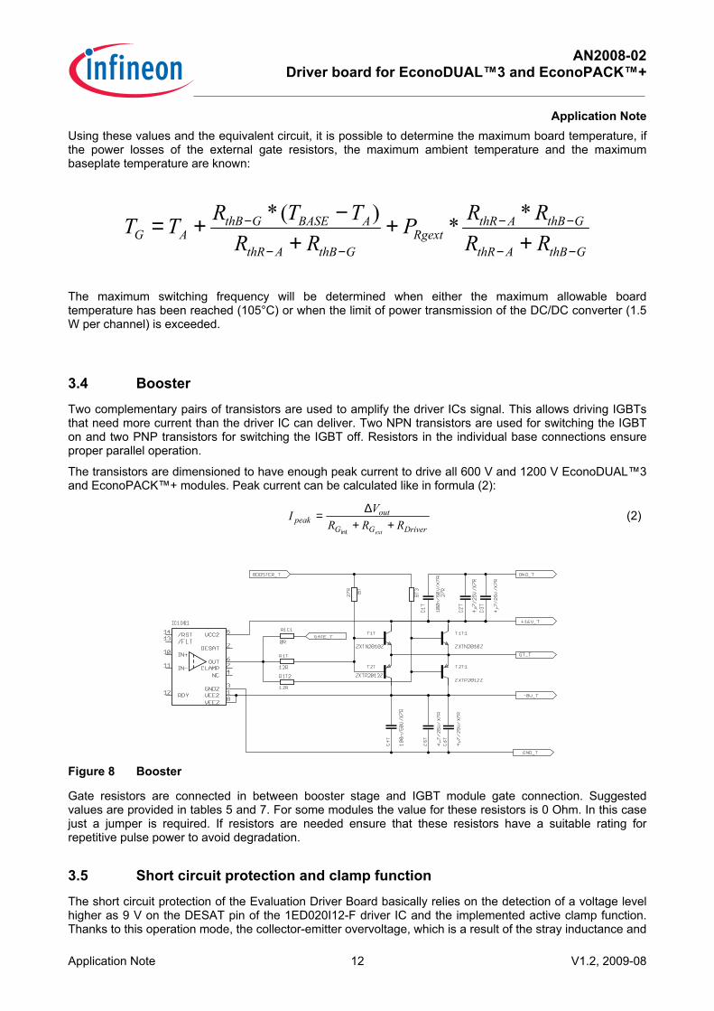
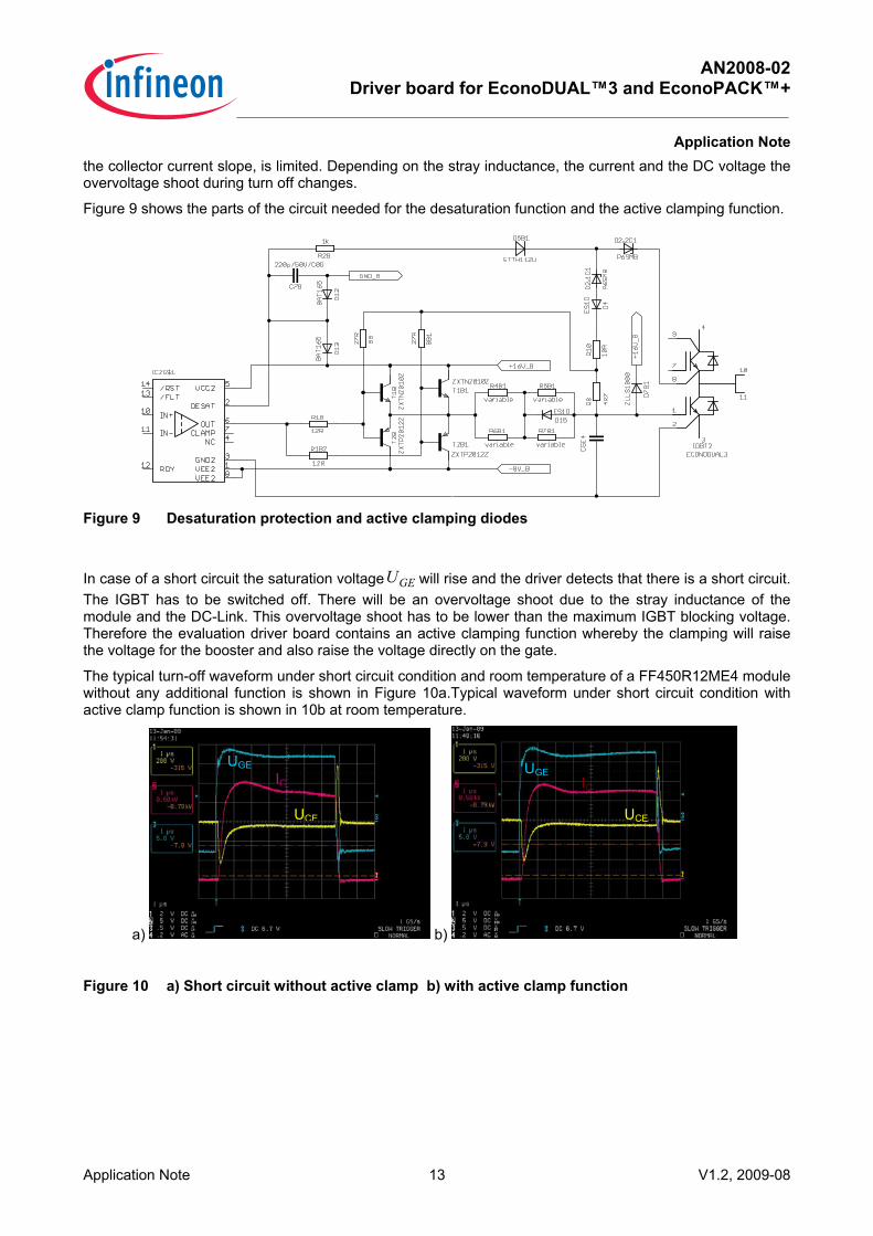
3.5 Short circuit protection and clamp function
The short circuit protection of the Evaluation Driver Board basically relies on the detection of a voltage level higher as 9 V on the DESAT pin of the 1ED020I12-F driver IC and the implemented active clamp function. Thanks to this operation mode, the collector-emitter overvoltage, which is a result of the stray inductance and
AN2008-02 Driver board for EconoDUAL™3 and EconoPACK™+
Application Note
Application Note 13 V1.2, 2009-08
the collector current slope, is limited. Depending on the stray inductance, the current and the DC voltage the overvoltage shoot during turn off changes.
Figure 9 shows the parts of the circuit needed for the desaturation function and the active clamping function.
Figure 9 Desaturation protection and active clamping diodes
In case of a short circuit the saturation voltage GEU will rise and the driver detects that there is a short circuit. The IGBT has to be switched off. There will be an overvoltage shoot due to the stray inductance of the module and the DC-Link. This overvoltage shoot has to be lower than the maximum IGBT blocking voltage. Therefore the evaluation driver board contains an active clamping function whereby the clamping will raise the voltage for the booster and also raise the voltage directly on the gate.
The typical turn-off waveform under short circuit condition and room temperature of a FF450R12ME4 module without any additional function is shown in Figure 10a.Typical waveform under short circuit condition with active clamp function is shown in 10b at room temperature.
a) b)
Figure 10 a) Short circuit without active clamp b) with active clamp function
UGE IC IC
UCE UCE
UGE
AN2008-02 Driver board for EconoDUAL™3 and EconoPACK™+
Application Note
Application Note 14 V1.2, 2009-08
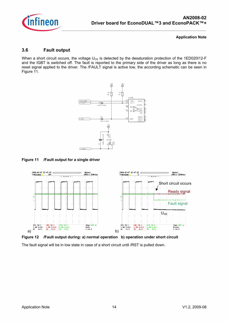
3.6 Fault output
When a short circuit occurs, the voltage UCE is detected by the desaturation protection of the 1ED020I12-F and the IGBT is switched off. The fault is reported to the primary side of the driver as long as there is no reset signal applied to the driver. The /FAULT signal is active low, the according schematic can be seen in Figure 11.
Figure 11 /Fault output for a single driver
a) b) Figure 12 /Fault output during: a) normal operation b) operation under short circuit
The fault signal will be in low state in case of a short circuit until /RST is pulled down.
Short circuit occurs
UGE
Fault signal
Ready signal
AN2008-02 Driver board for EconoDUAL™3 and EconoPACK™+
Application Note
Application Note 15 V1.2, 2009-08
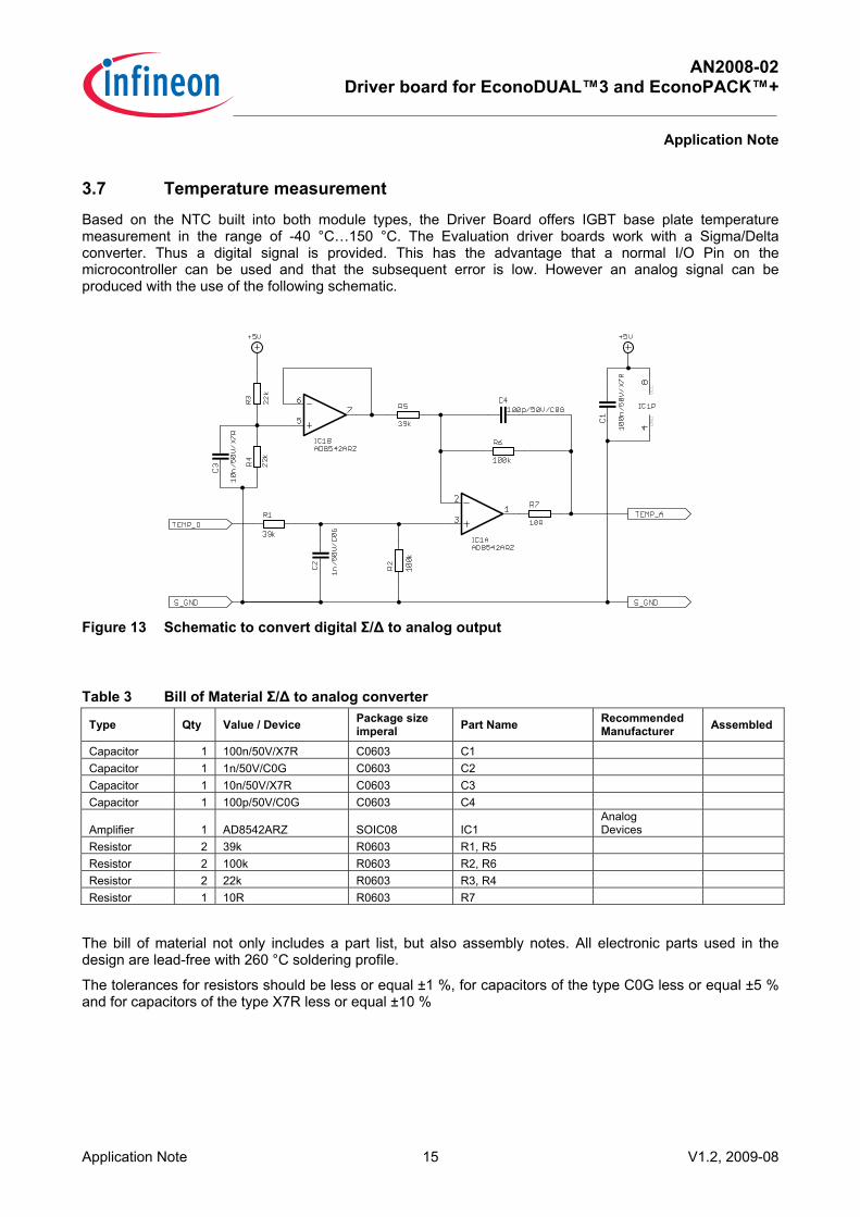
3.7 Temperature measurement
Based on the NTC built into both module types, the Driver Board offers IGBT base plate temperature measurement in the range of -40 °C…150 °C. The Evaluation driver boards work with a Sigma/Delta converter. Thus a digital signal is provided. This has the advantage that a normal I/O Pin on the microcontroller can be used and that the subsequent error is low. However an analog signal can be produced with the use of the following schematic.
Figure 13 Schematic to convert digital Σ/∆ to analog output
Table 3 Bill of Material Σ/∆ to analog converter
Type Qty Value / Device Package size imperal Part Name Recommended
Manufacturer Assembled
Capacitor 1 100n/50V/X7R C0603 C1 Capacitor 1 1n/50V/C0G C0603 C2 Capacitor 1 10n/50V/X7R C0603 C3 Capacitor 1 100p/50V/C0G C0603 C4
Amplifier 1 AD8542ARZ SOIC08 IC1 Analog Devices
Resistor 2 39k R0603 R1, R5 Resistor 2 100k R0603 R2, R6 Resistor 2 22k R0603 R3, R4 Resistor 1 10R R0603 R7
The bill of material not only includes a part list, but also assembly notes. All electronic parts used in the design are lead-free with 260 °C soldering profile.
The tolerances for resistors should be less or equal ±1 %, for capacitors of the type C0G less or equal ±5 % and for capacitors of the type X7R less or equal ±10 %
AN2008-02 Driver board for EconoDUAL™3 and EconoPACK™+
Switching losses
Application Note 16 V1.2, 2009-08
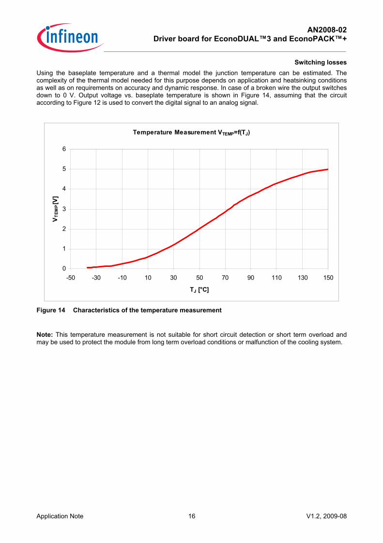
Using the baseplate temperature and a thermal model the junction temperature can be estimated. The complexity of the thermal model needed for this purpose depends on application and heatsinking conditions as well as on requirements on accuracy and dynamic response. In case of a broken wire the output switches down to 0 V. Output voltage vs. baseplate temperature is shown in Figure 14, assuming that the circuit according to Figure 12 is used to convert the digital signal to an analog signal.
Temperature Measurement VTEMP=f(TJ)
0
1
2
3
4
5
6
-50 -30 -10 10 30 50 70 90 110 130 150
TJ [°C]
VTE
MP [V
]
Figure 14 Characteristics of the temperature measurement
Note: This temperature measurement is not suitable for short circuit detection or short term overload and may be used to protect the module from long term overload conditions or malfunction of the cooling system.
AN2008-02 Driver board for EconoDUAL™3 and EconoPACK™+
Switching losses
Application Note 17 V1.2, 2009-08
4 Switching losses The setup used for preparing this application note varies from the setup used to characterize the devices in three aspects:
DC-link inductance:
The DC-link inductance of the setup used for these test is has a value of approximately 35 nH for all modules investigated here in contrast to varying values between 35 nH to 80 nH used for device characterization (see device datasheets for details). For a detailed discussion on the impact of DC-link inductance on switching losses please refer to [2].
Gate voltage:
This Evaluation Board provides a gate voltage of -8 V for turning off and 16 V for turning on wheras charactization is done with a driver providing +/- 15 V of gate voltage.
Gate driver output impedance:
According to IEC 60747-9 for characterization of an IGBT the driver used should resemble an ideal voltage source as far as possible. For the Evaluation Board a driver output stage has been choosen that considers board space as well as cost constraints. Therefore it can not provide close to zero output impedance.
All aspects discussed above have an impact on the switching speed of the module and hence also on the switching losses. Gate resistor values have been choosen so that di/dt at turn-on compareable to characterization has been achieved. Nevertheless small deviations in the turn-on losses persist. For the turn-off losses there is little impact of driving conditions for trench-fieldstop IGBTs like the ME3 and ME4 devices. For NPT IGBTs, like used in the MS4 modules, the considerations made for turn-on losses also apply for turn-off losses.
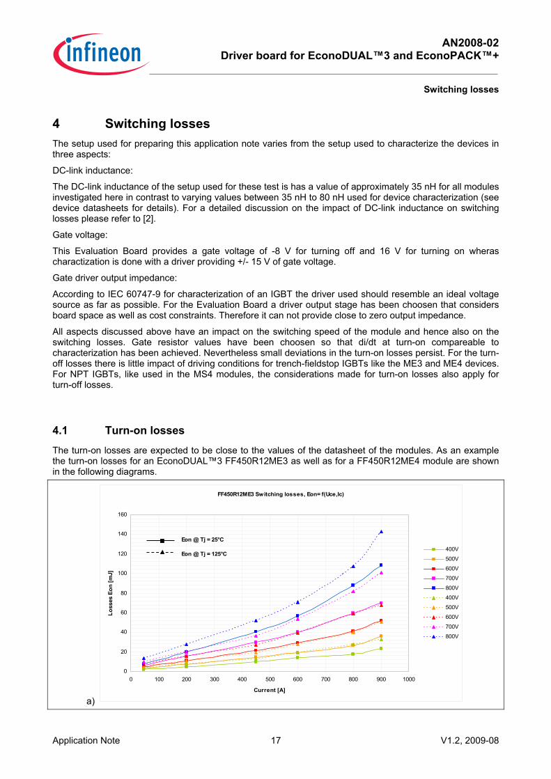
4.1 Turn-on losses
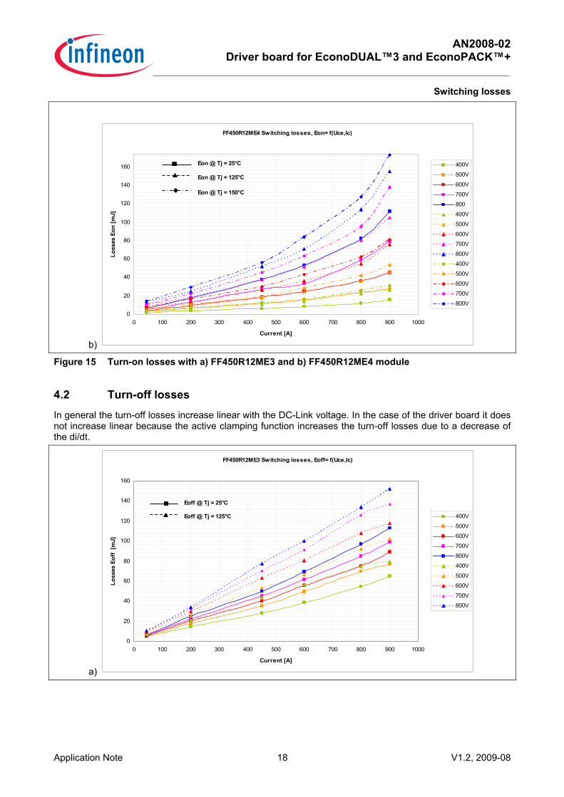
The turn-on losses are expected to be close to the values of the datasheet of the modules. As an example the turn-on losses for an EconoDUAL™3 FF450R12ME3 as well as for a FF450R12ME4 module are shown in the following diagrams.
a)
FF450R12ME3 Switching losses, Eon= f(Uce,Ic)
0
20
40
60
80
100
120
140
160
0 100 200 300 400 500 600 700 800 900 1000
Current [A]
Loss
es E
on [m
J]
400V
500V
600V
700V
800V
400V
500V
600V
700V
800V
Eon @ Tj = 25°C
Eon @ Tj = 125°C
AN2008-02 Driver board for EconoDUAL™3 and EconoPACK™+
Switching losses
Application Note 18 V1.2, 2009-08
b)
FF450R12ME4 Switching losses, Eon= f(Uce,Ic)
0
20
40
60
80
100
120
140
160
0 100 200 300 400 500 600 700 800 900 1000
Current [A]
Loss
es E
on [m
J]
400V
500V
600V
700V
800
400V
500V
600V
700V
800V
400V
500V
600V
700V
800V
Eon @ Tj = 25°C
Eon @ Tj = 125°C
Eon @ Tj = 150°C
Figure 15 Turn-on losses with a) FF450R12ME3 and b) FF450R12ME4 module
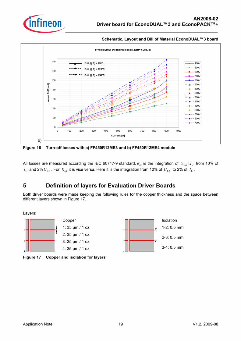
4.2 Turn-off losses
In general the turn-off losses increase linear with the DC-Link voltage. In the case of the driver board it does not increase linear because the active clamping function increases the turn-off losses due to a decrease of the di/dt.
a)
FF450R12ME3 Switching losses, Eoff= f(Uce,Ic)
0
20
40
60
80
100
120
140
160
0 100 200 300 400 500 600 700 800 900 1000
Current [A]
Loss
es E
off
[mJ]
400V
500V
600V
700V
800V
400V
500V
600V
700V
800V
Eoff @ Tj = 25°C
Eoff @ Tj = 125°C
AN2008-02 Driver board for EconoDUAL™3 and EconoPACK™+
Schematic, Layout and Bill of Material EconoDUAL™3 board
Application Note 19 V1.2, 2009-08
b)
FF450R12ME4 Switching losses, Eoff= f(Uce,Ic)
0
20
40
60
80
100
120
140
0 100 200 300 400 500 600 700 800 900 1000
Current [A]
Loss
es E
off [
mJ]
400V
500V
600V
700V
800V
400V
500V
600V
700V
800V
400V
500V
600V
800V
700V
Eoff @ Tj = 25°C
Eoff @ Tj = 125°C
Eoff @ Tj = 150°C
Figure 16 Turn-off losses with a) FF450R12ME3 and b) FF450R12ME4 module
All losses are measured according the IEC 60747-9 standard. onE is the integration of CCE IU ⋅ from 10% of
CI and 2% CEU . For offE it is vice versa. Here it is the integration from 10% of CEU to 2% of CI .
5 Definition of layers for Evaluation Driver Boards Both driver boards were made keeping the following rules for the copper thickness and the space between different layers shown in Figure 17.
Layers:
Figure 17 Copper and isolation for layers
Copper Isolation
1: 35 µm / 1 oz.
2: 35 µm / 1 oz.
3: 35 µm / 1 oz.
4: 35 µm / 1 oz.
1-2: 0.5 mm
2-3: 0.5 mm
3-4: 0.5 mm
AN2008-02 Driver board for EconoDUAL™3 and EconoPACK™+
Schematic, Layout and Bill of Material EconoDUAL™3 board
Application Note 20 V1.2, 2009-08
6 Schematic, Layout and Bill of Material EconoDUAL™3 board To meet the individual customer requirement and make the Evaluation Driver Board for the EconoDUAL™3 module simple for development or modification, all necessary technical data like schematic, layout and components are included in this chapter.
6.1 Schematic
Figure 18 IGBT driver – Top transistor
Figure 19 IGBT driver – Bottom transistor
AN2008-02 Driver board for EconoDUAL™3 and EconoPACK™+
Schematic, Layout and Bill of Material EconoDUAL™3 board
Application Note 21 V1.2, 2009-08
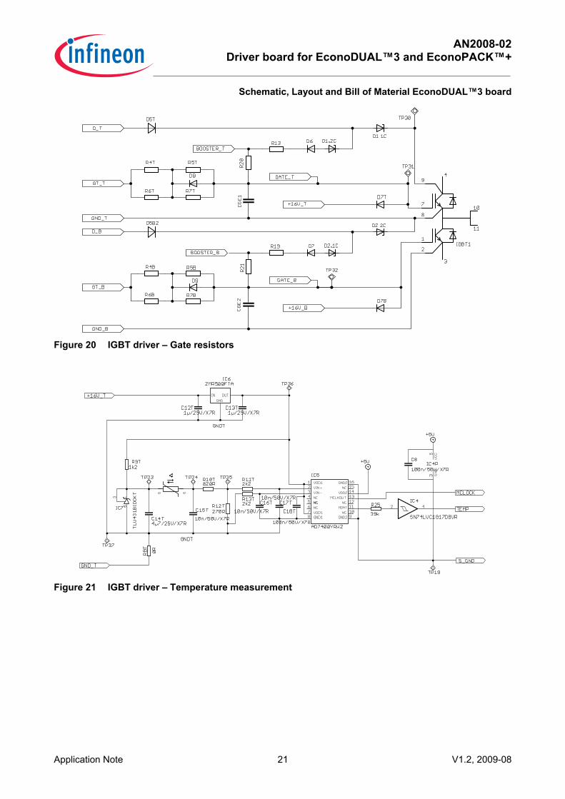
Figure 20 IGBT driver – Gate resistors
Figure 21 IGBT driver – Temperature measurement
AN2008-02 Driver board for EconoDUAL™3 and EconoPACK™+
Schematic, Layout and Bill of Material EconoDUAL™3 board
Application Note 22 V1.2, 2009-08
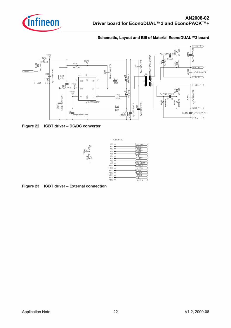
Figure 22 IGBT driver – DC/DC converter
Figure 23 IGBT driver – External connection
AN2008-02 Driver board for EconoDUAL™3 and EconoPACK™+
Schematic, Layout and Bill of Material EconoDUAL™3 board
Application Note 23 V1.2, 2009-08
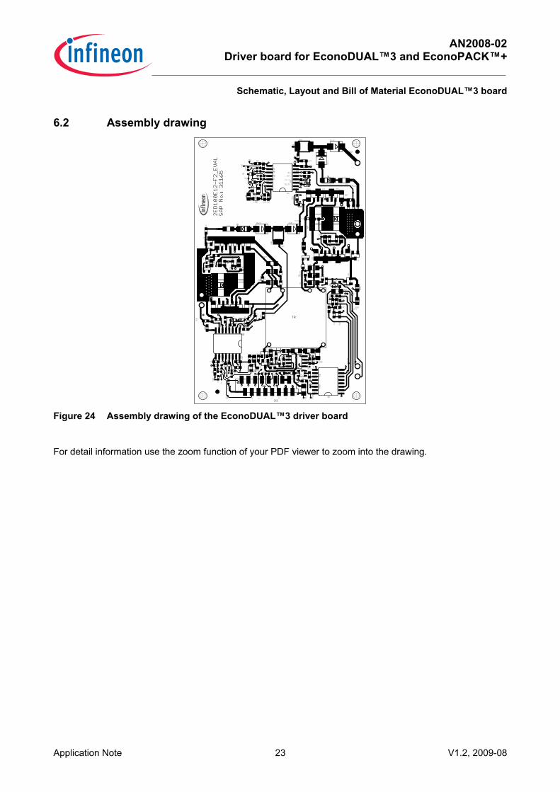
6.2 Assembly drawing
Figure 24 Assembly drawing of the EconoDUAL™3 driver board
For detail information use the zoom function of your PDF viewer to zoom into the drawing.
AN2008-02 Driver board for EconoDUAL™3 and EconoPACK™+
Schematic, Layout and Bill of Material EconoDUAL™3 board
Application Note 24 V1.2, 2009-08
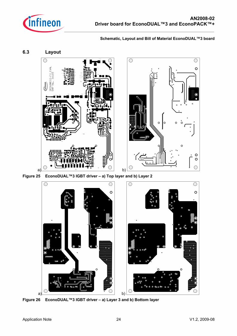
6.3 Layout
a) b) Figure 25 EconoDUAL™3 IGBT driver – a) Top layer and b) Layer 2
a) b) Figure 26 EconoDUAL™3 IGBT driver – a) Layer 3 and b) Bottom layer
AN2008-02 Driver board for EconoDUAL™3 and EconoPACK™+
Schematic, Layout and Bill of Material EconoDUAL™3 board
Application Note 25 V1.2, 2009-08
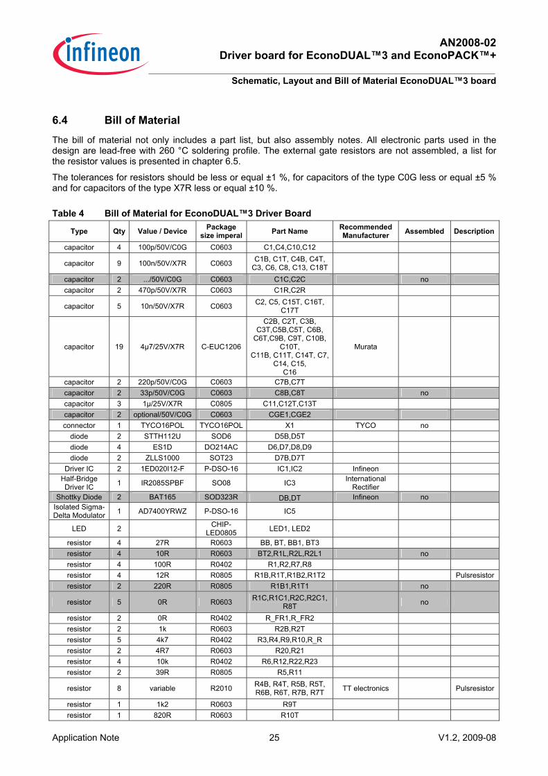
6.4 Bill of Material
The bill of material not only includes a part list, but also assembly notes. All electronic parts used in the design are lead-free with 260 °C soldering profile. The external gate resistors are not assembled, a list for the resistor values is presented in chapter 6.5.
The tolerances for resistors should be less or equal ±1 %, for capacitors of the type C0G less or equal ±5 % and for capacitors of the type X7R less or equal ±10 %.
Table 4 Bill of Material for EconoDUAL™3 Driver Board
Type Qty Value / Device Package size imperal Part Name Recommended
Manufacturer Assembled Description
capacitor 4 100p/50V/C0G C0603 C1,C4,C10,C12
capacitor 9 100n/50V/X7R C0603 C1B, C1T, C4B, C4T, C3, C6, C8, C13, C18T
capacitor 2 .../50V/C0G C0603 C1C,C2C no capacitor 2 470p/50V/X7R C0603 C1R,C2R
capacitor 5 10n/50V/X7R C0603 C2, C5, C15T, C16T, C17T
capacitor 19 4µ7/25V/X7R C-EUC1206
C2B, C2T, C3B, C3T,C5B,C5T, C6B,
C6T,C9B, C9T, C10B, C10T,
C11B, C11T, C14T, C7, C14, C15,
C16
Murata
capacitor 2 220p/50V/C0G C0603 C7B,C7T capacitor 2 33p/50V/C0G C0603 C8B,C8T no capacitor 3 1µ/25V/X7R C0805 C11,C12T,C13T capacitor 2 optional/50V/C0G C0603 CGE1,CGE2 connector 1 TYCO16POL TYCO16POL X1 TYCO no
diode 2 STTH112U SOD6 D5B,D5T diode 4 ES1D DO214AC D6,D7,D8,D9 diode 2 ZLLS1000 SOT23 D7B,D7T
Driver IC 2 1ED020I12-F P-DSO-16 IC1,IC2 Infineon Half-Bridge Driver IC 1 IR2085SPBF SO08 IC3 International
Rectifier
Shottky Diode 2 BAT165 SOD323R DB,DT Infineon no Isolated Sigma-Delta Modulator 1 AD7400YRWZ P-DSO-16 IC5
LED 2 CHIP-LED0805 LED1, LED2
resistor 4 27R R0603 BB, BT, BB1, BT3 resistor 4 10R R0603 BT2,R1L,R2L,R2L1 no resistor 4 100R R0402 R1,R2,R7,R8 resistor 4 12R R0805 R1B,R1T,R1B2,R1T2 Pulsresistor resistor 2 220R R0805 R1B1,R1T1 no
resistor 5 0R R0603 R1C,R1C1,R2C,R2C1,R8T no
resistor 2 0R R0402 R_FR1,R_FR2 resistor 2 1k R0603 R2B,R2T resistor 5 4k7 R0402 R3,R4,R9,R10,R_R resistor 2 4R7 R0603 R20,R21 resistor 4 10k R0402 R6,R12,R22,R23 resistor 2 39R R0805 R5,R11
resistor 8 variable R2010 R4B, R4T, R5B, R5T, R6B, R6T, R7B, R7T TT electronics Pulsresistor
resistor 1 1k2 R0603 R9T resistor 1 820R R0603 R10T
AN2008-02 Driver board for EconoDUAL™3 and EconoPACK™+
Schematic, Layout and Bill of Material EconoPACK™+ board
Application Note 26 V1.2, 2009-08
resistor 3 2k2 R0603 R11T,R13T,R17 resistor 1 270R R0603 R12T resistor 2 10R R1206 R13,R19 resistor 2 15R R0603 R15,R16 resistor 1 68k R0603 R14 resistor 1 0R15 R0805 R18 resistor 1 39k R0603 R25
Schmitt-Trigger 1 SN74LVC1G17DBVR SOT23-5 IC4
Shottky Diode 17 BAT165 SOD323R
D2B,D2R,D2T,D3, D3B,D3T,D4,D4B, D4T,D5,D10,D11,
D12,D13,D1, D1R,D2
Infineon
Shunt Regulator 1 TLV431BIDCKT SC70-6L IC7
Transformer 1 T60403-D4615-X054 D4615-X054 TR Vacuum-
schmelze
Transistor 2 BC856 SOT23 T1,T2 Infineon Transistor 4 ZXTN2010Z SOT89 T1B, T1B1, T1T, T1T1 Zetex Transistor 4 ZXTP2012Z SOT89 T2B, T2B1, T2T, T2T1 Zetex
TrenchMOS 2 PMV45EN SOT23 T3,T4 philips Unipolar TVS
Diode 2 P6SMB440A SMB D1.1C,D2.1C Vishay
Unipolar TVS Diode 2 P6SMB510A SMB D2.1C,D2.2C Vishay
Zener diode 4 MM3Z5V6T1G SOD323-R D1.1B, D1.1T, D1.2B, D1.2T
On Semiconductor no
Zener diode 1 ZMR500FTA SOT23 IC6 Zener diode 2 BZX84-C11 SOT23 ZB,ZT no
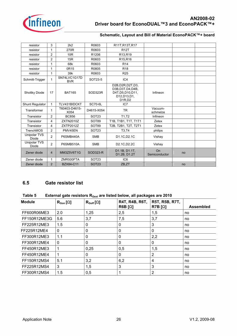
6.5 Gate resistor list
Table 5 External gate resistors RGext are listed below, all packages are 2010 Module RGon [Ω] RGoff [Ω] R4T, R4B, R6T,
R6B [Ω] R5T, R5B, R7T, R7B [Ω]
Assembled FF600R06ME3 2.0 1,25 2,5 1,5 no FF150R12ME3G 5.6 3,7 7,5 3,7 no FF225R12ME3 1.5 0 0 3 no FF225R12ME4 0 0 0 0 no FF300R12ME3 1.1 0 0 2,2 no FF300R12ME4 0 0 0 0 no FF450R12ME3 1 0,25 0,5 1,5 no FF450R12ME4 1 0 0 2 no FF150R12MS4 5.1 3,2 6,2 4 no FF225R12MS4 3 1,5 3 3 no FF300R12MS4 1.5 0,5 1 2 no
AN2008-02 Driver board for EconoDUAL™3 and EconoPACK™+
Schematic, Layout and Bill of Material EconoPACK™+ board
Application Note 27 V1.2, 2009-08
7 Schematic, Layout and Bill of Material EconoPACK™+ board To meet the individual customer requirement and make the Evaluation Driver Board for the EconoPACK™+ module a simple for development or modification, all necessary technical data like schematic, layout and components are included in this chapter.
The tolerances for resistors should be less or equal ±1 %, for capacitors of the type C0G less or equal ±5 % and for capacitors of the type X7R less or equal ±10 %.
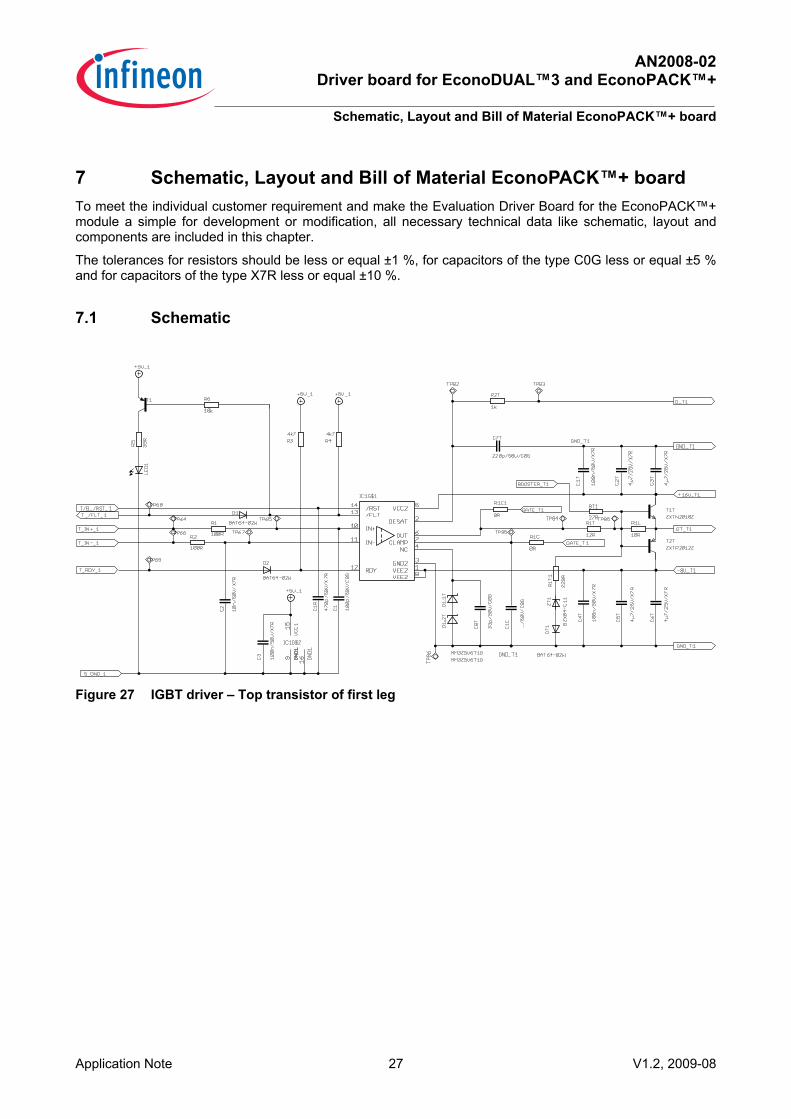
7.1 Schematic
Figure 27 IGBT driver – Top transistor of first leg
AN2008-02 Driver board for EconoDUAL™3 and EconoPACK™+
Schematic, Layout and Bill of Material EconoPACK™+ board
Application Note 28 V1.2, 2009-08
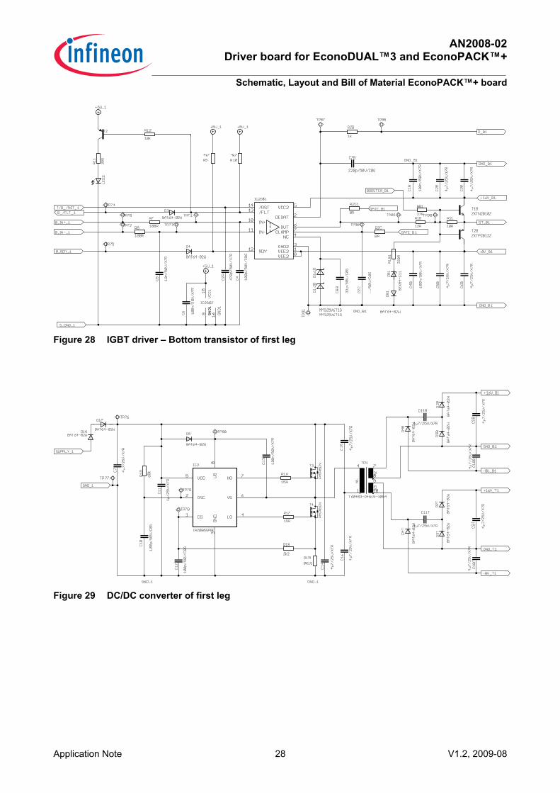
Figure 28 IGBT driver – Bottom transistor of first leg
Figure 29 DC/DC converter of first leg
AN2008-02 Driver board for EconoDUAL™3 and EconoPACK™+
Schematic, Layout and Bill of Material EconoPACK™+ board
Application Note 29 V1.2, 2009-08
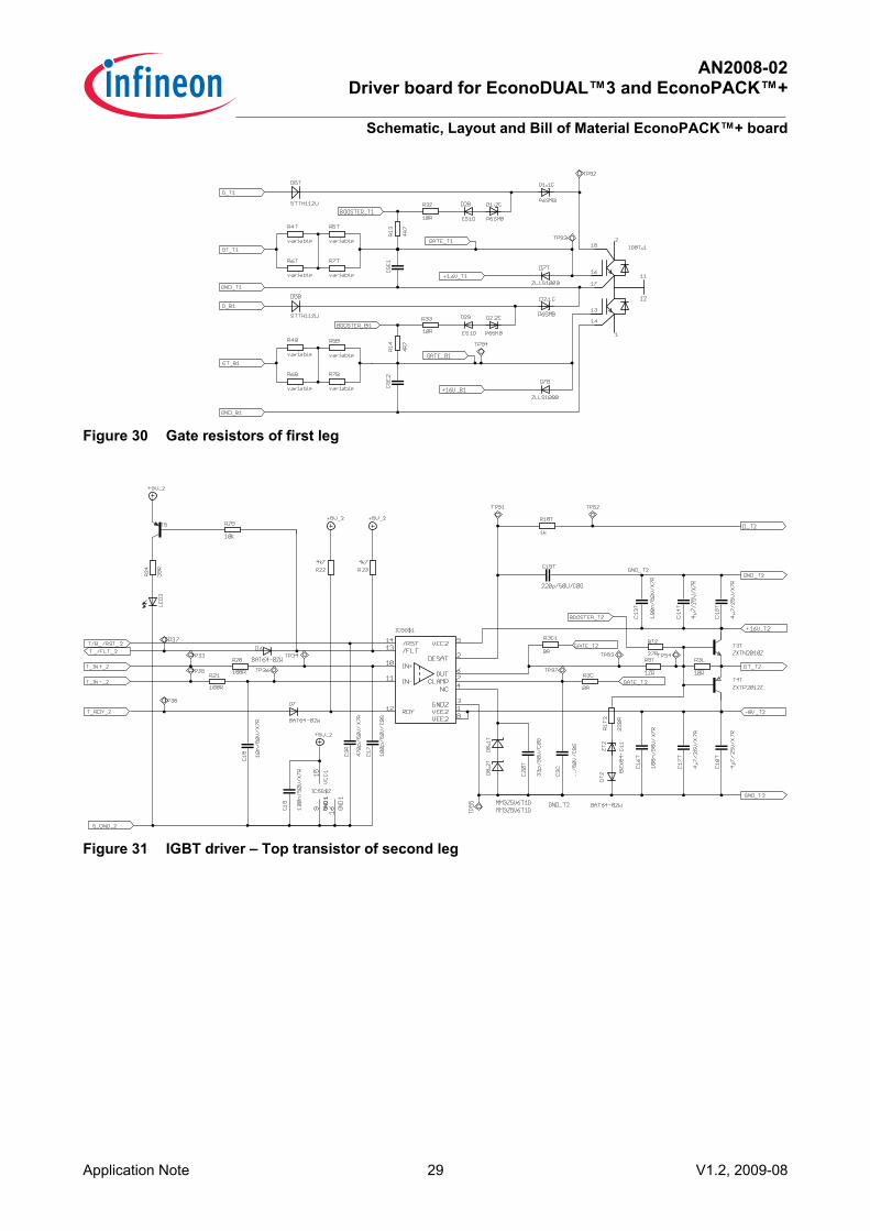
Figure 30 Gate resistors of first leg
Figure 31 IGBT driver – Top transistor of second leg
AN2008-02 Driver board for EconoDUAL™3 and EconoPACK™+
Schematic, Layout and Bill of Material EconoPACK™+ board
Application Note 30 V1.2, 2009-08
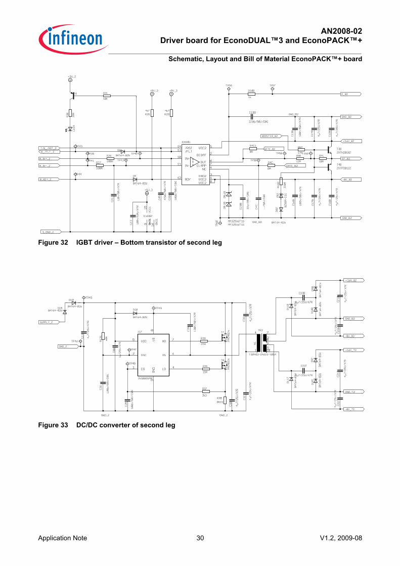
Figure 32 IGBT driver – Bottom transistor of second leg
Figure 33 DC/DC converter of second leg
AN2008-02 Driver board for EconoDUAL™3 and EconoPACK™+
Schematic, Layout and Bill of Material EconoPACK™+ board
Application Note 31 V1.2, 2009-08
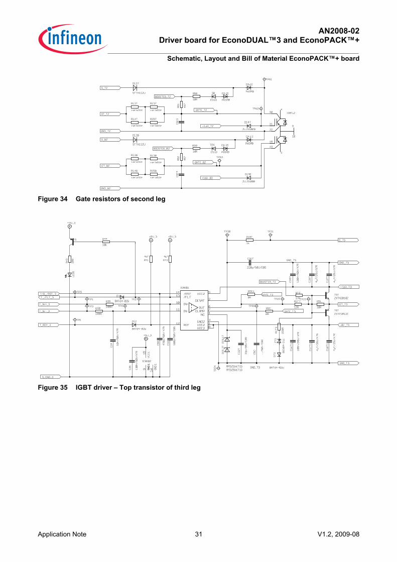
Figure 34 Gate resistors of second leg
Figure 35 IGBT driver – Top transistor of third leg
AN2008-02 Driver board for EconoDUAL™3 and EconoPACK™+
Schematic, Layout and Bill of Material EconoPACK™+ board
Application Note 32 V1.2, 2009-08
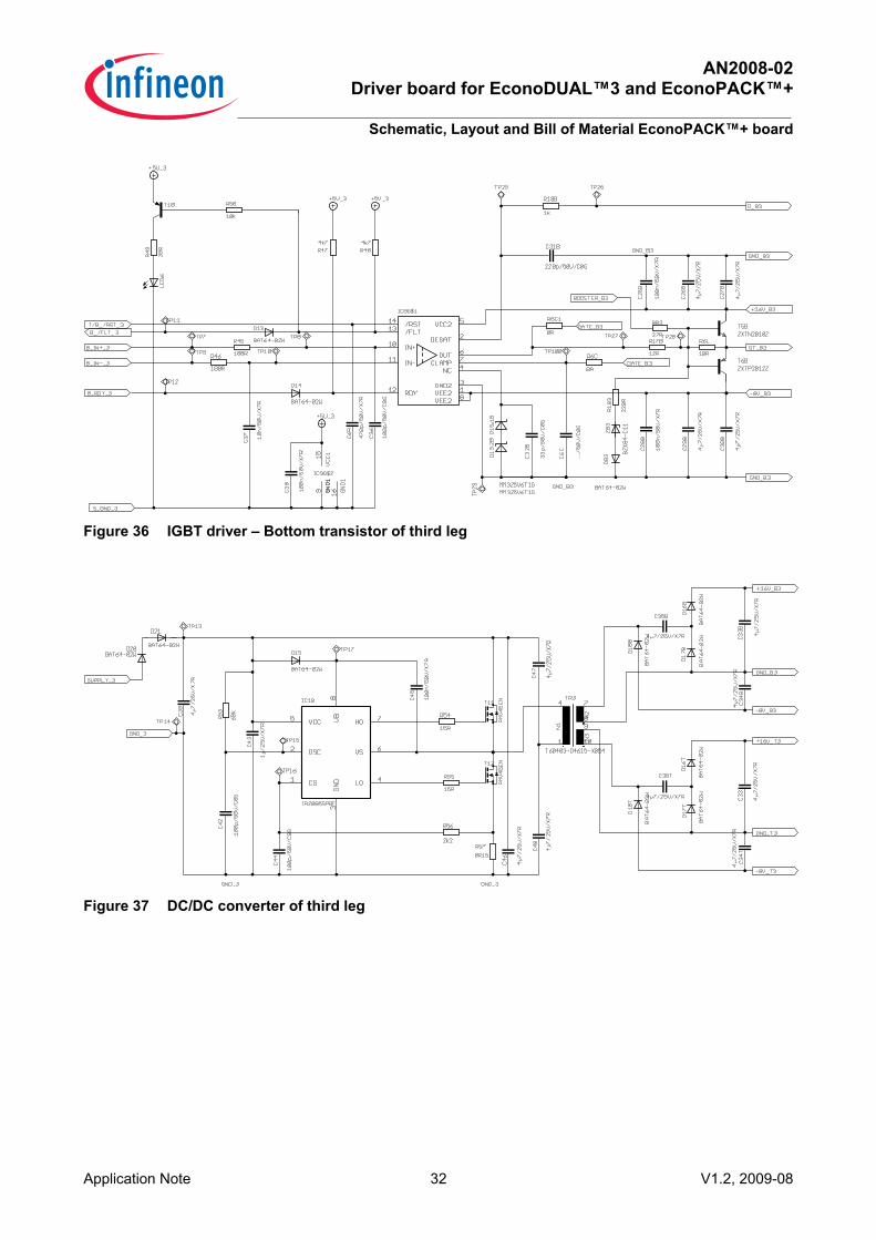
Figure 36 IGBT driver – Bottom transistor of third leg
Figure 37 DC/DC converter of third leg
AN2008-02 Driver board for EconoDUAL™3 and EconoPACK™+
Schematic, Layout and Bill of Material EconoPACK™+ board
Application Note 33 V1.2, 2009-08
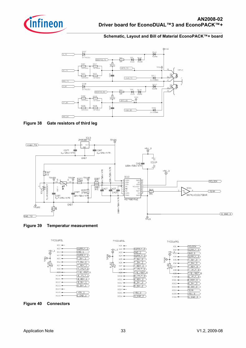
Figure 38 Gate resistors of third leg
Figure 39 Temperatur measurement
Figure 40 Connectors
AN2008-02 Driver board for EconoDUAL™3 and EconoPACK™+
Schematic, Layout and Bill of Material EconoPACK™+ board
Application Note 34 V1.2, 2009-08
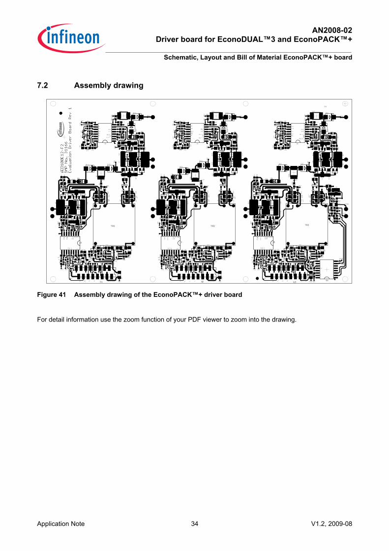
7.2 Assembly drawing
Figure 41 Assembly drawing of the EconoPACK™+ driver board
For detail information use the zoom function of your PDF viewer to zoom into the drawing.
AN2008-02 Driver board for EconoDUAL™3 and EconoPACK™+
Schematic, Layout and Bill of Material EconoPACK™+ board
Application Note 35 V1.2, 2009-08
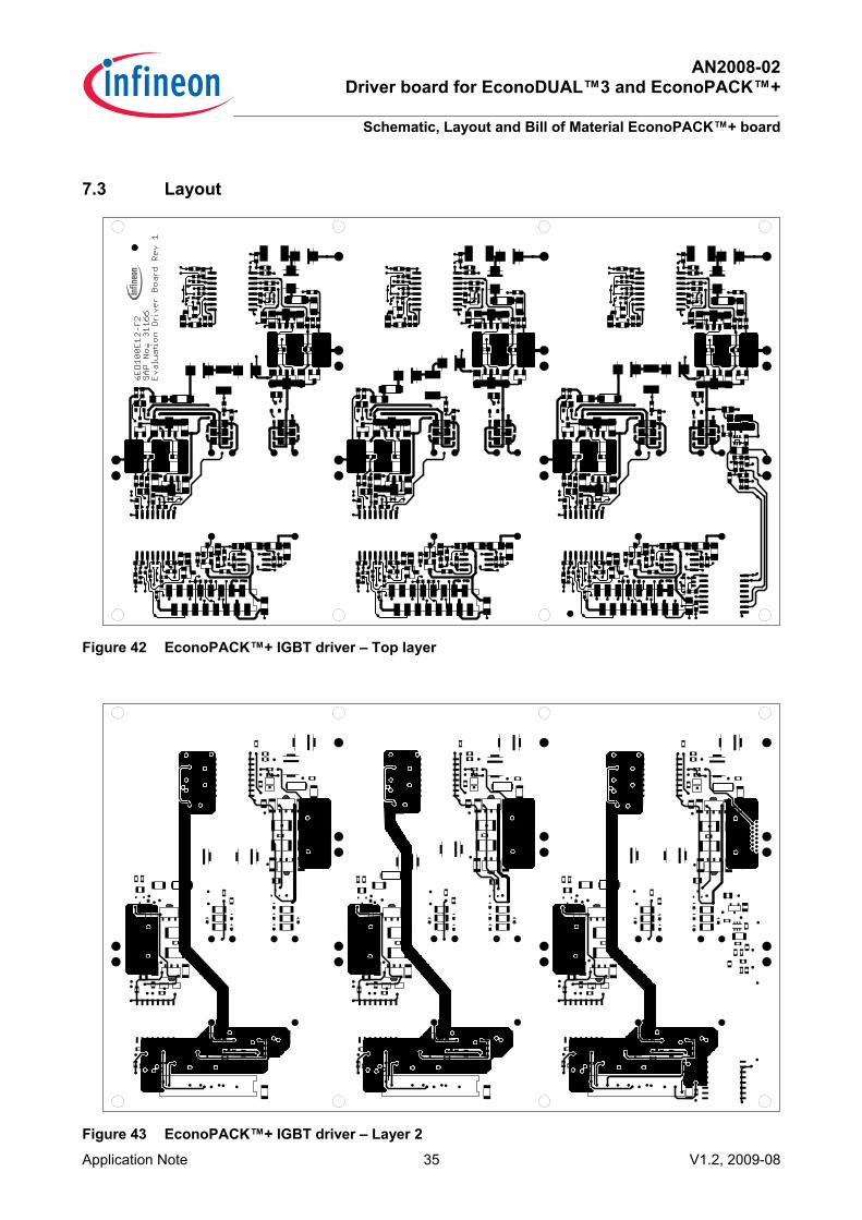
7.3 Layout
Figure 42 EconoPACK™+ IGBT driver – Top layer
Figure 43 EconoPACK™+ IGBT driver – Layer 2
AN2008-02 Driver board for EconoDUAL™3 and EconoPACK™+
Schematic, Layout and Bill of Material EconoPACK™+ board
Application Note 36 V1.2, 2009-08
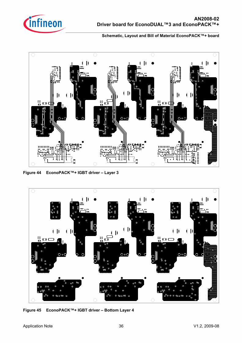
Figure 44 EconoPACK™+ IGBT driver – Layer 3
Figure 45 EconoPACK™+ IGBT driver – Bottom Layer 4
AN2008-02 Driver board for EconoDUAL™3 and EconoPACK™+
Schematic, Layout and Bill of Material EconoPACK™+ board
Application Note 37 V1.2, 2009-08
7.4 Bill of material
The bill of material not only includes a part list, but also assembly notes. All electronic parts used in the design are lead-free with 260 °C soldering profile. The external gate resistors are not assembled, a list for the resistor values is presented in chapter 7.5.
Table 6 Bill of Material for EconoPACK™+ Driver Board Type Qty Value / Device Package size
imperal Part Name Recommended
Manufacturer Assembled
Capacitor 6 .../50V/C0G C0603 C1C, C2C, C3C, C4C, C5C, C6C
no
Capacitor 9 10n/50V/X7R C0603 C2, C5, C18, C21, C34, C37, C40T, C41T, C42T
Capacitor 6 33p/50V/C0G C0603 C8B, C8T, C20B, C20T, C32B, C32T
no
Capacitor 23 100n/50V/X7R C0603 C1B, C1T, C3, C4B, C4T, C6, C13, C13B, C13T, C16B, C16T, C19, C22, C25B, C25T, C28B, C28T, C29, C35, C38, C43T, C45, C49
Capacitor 12 100p/50V/C0G C0603 C1, C4, C10, C12, C17, C20, C26, C28, C33, C36, C42, C44
Capacitor 6 220p/50V/C0G C0603 C7B, C7T, C19B, C19T, C31B, C31T
Capacitor 6 470p/50V/X7R C0603 C1R, C2R, C3R, C4R, C5R, C6R
Capacitor 6 optional/50V/C0G C0603 CGE1, CGE2, CGE3, CGE4, CGE5, CGE6
no
Capacitor 5 1µ/25V/X7R C0805 C11, C27, C37T, C38T, C43
Capacitor 55 4µ7/25V/X7R C1206 C2B, C2T, C3B, C3T, C5B, C5T, C6B, C6T, C7, C9B, C9T, C10B, C10T, C11B, C11T, C14, C14B, C14T, C15, C15B, C15T, C16, C17B, C17T, C18B, C18T, C21B, C21T, C22B, C22T, C23, C23B, C23T, C26B, C26T, C27B, C27T, C29B, C29T, C30, C30B, C30T, C31, C32, C33B, C33T, C34B, C34T, C35B, C35T, C39, C39T, C46, C47, C48
Murata
Transformer 3 T60403- D4615-X054 TR1, TR2, TR3 Vacuum- schmelze
LED 6 LEDCHIP- LED0805 LED1, LED2, LED3, LED4, LED5, LED6
Schottky Diodes
39 BAT64-02W SCD80 D1, D2, D2B, D2T, D3, D3B, D3T, D4, D4B, D4T, D5, D6, D7, D8, D9, D9B, D9T, D10, D10B, D10T, D11, D11B, D11T, D12, D13, D14, D15, D16, D16B, D16T, D17, D17B, D17T, D18, D18B, D18T, D19, D20, D21
Infineon
Rectifier Diode
6 ES1D DO214AC D28, D29, D30, D31, D32, D33
AN2008-02 Driver board for EconoDUAL™3 and EconoPACK™+
Schematic, Layout and Bill of Material EconoPACK™+ board
Application Note 38 V1.2, 2009-08
Type Qty Value / Device Package size imperal
Part Name Recommended Manufacturer
Assembled
Diode 6 BAT64-02W SCD80 DB1, DB2, DB3, DT1, DT2, DT3
Infineon no
Unipolar TVS Diode
6 P6SMB/440V SMB D1.1C, D2.1C, D3.1C, D4.1C, D5.1C, D6.1C,
Unipolar TVS Diode
6 P6SMB/510V SMB D1.2C, D2.2C, D3.2C, D4.2C, D5.2C, D6.2C
Diode 6 STTA112U SOD6 D5B, D5T, D12B, D12T, D19B, D19T
Zener Diode 12 MM3Z5V6T1G SOD323-R D1.1B, D1.1T, D1.2B, D1.2T, D8.1B, D8.1T, D8.2B, D8.2T, D15.1B, D15.1T, D15.2B, D15.2T
On Semiconductor
no
Zener Diode 6 BZX84-C11 SOT23 ZB1, ZB2, ZB3, ZT1, ZT2, ZT3
no
Diode 6 ZLLS1000 SOT23 D7B, D7T, D14B, D14T, D21B, D21T
Zetex
Driver IC 6 1ED020I12-F P-DSO-16 IC1, IC2, IC5, IC6, IC8, IC9
Half-Bridge Driver
3 IR2085SPBF SO08 IC3, IC7, IC10 International Rectifier
Schmitt-Trigger
1 SN74LVC1G17DBVR SOT23-5 IC11
Isolated Sigma-Delta Modulator
1 AD7400YRWZ P-DSO-16 IC12 Analog Devices
Voltage regulator
1 ZMR500FTA SOT23 IC13
Shunt Regulator
1 TLV431BIDCKT SC70-6L IC14
Resistor 6 0R R0402 R_FR1, R_FR2, R_FR3, R_FR4, R_FR5, R_FR6
Resistor 15 4k7 R0402 R_R1, R_R2, R_R3, R3, R4, R9, R10, R22, R23, R28, R29, R41, R42, R47, R48
Resistor 6 10k R0402 R6, R12, R25, R31, R44, R50
Resistor 12 100R R0402 R1, R2, R7, R8, R20, R21, R26, R27, R39, R40, R45, R46
Resistor 7 0R R0603 R1C, R2C, R3C, R4C, R5C, R6C, R25T
no
Resistor 6 0R R0603 R1C1, R2C1, R3C1, R4C1, R5C1, R6C1
no
Resistor 6 27R R0603 BB1, BB2, BB3, BT1, BT2, BT3
Resistor 6 1k R0603 R2B, R2T, R10B, R10T, R18B, R18T
Resistor 1 1k2 R0603 R26T Resistor 5 2k2 R0603 R18, R28T, R30T, R37,
R56
Resistor 6 4R7 R0603 R13, R14, R51, R52, R60, R61
Resistor 6 10R R0603 R1L, R2L, R3L, R4L, R5L, R6L
no
Resistor 6 15R R0603 R16, R17, R35, R36, R54, R55
Resistor 1 39k R0603 R64 Resistor 3 68k R0603 R15, R34, R53 Resistor 1 270R R0603 R29T Resistor 1 820R R0603 R27T Resistor 3 0R15 R0805 R19, R38, R57
AN2008-02 Driver board for EconoDUAL™3 and EconoPACK™+
How to order Evaluation Driver Boards
Application Note 39 V1.2, 2009-08
Type Qty Value / Device Package size imperal
Part Name Recommended Manufacturer
Assembled
Resistor 6 12R R0805 R1B, R1T, R9B, R9T, R17B, R17T
Resistor 6 39R R0805 R5, R11, R24, R30, R43, R49
Resistor 6 220R R0805 R1B1, R1B2, R1B3, R1T1, R1T2, R1T3
no
Resistor 6 10R R1206 R32, R33, R58, R59, R62, R63
Resistor 24 variable R2010 R4B, R4T, R5B, R5T, R6B, R6T, R7B, R7T, R12B, R12T, R13B, R13T, R14B, R14T, R15B, R15T, R20B, R20T, R21B, R21T, R22B, R22T, R23B, R23T
TT electronics no: See Table 8
Transistor 6 BC856 SOT23 T1, T2, T5, T6, T9, T10 TrenchMOS 6 PMV45EN SOT23 T3, T4, T7, T8, T11,
T12 Philips
Transistor 6 ZXTN2010Z SOT89 T1B, T1T, T3B, T3T, T5B, T5T
Zetex
Transistor 6 ZXTP2012Z SOT89 T2B, T2T, T4B, T4T, T6B, T6T
Zetex
Connector 3 8-188275-6 16POL X1, X2, X3 Tyco
7.5 Gate resistor list
Table 7 External gate resistors RGext are listed below, all packages are 2010 Module RGext [Ω] R4T, R4B, R6T, R6B [Ω]
R12T, R12B, R14T, R14B [Ω] R20T, R20B, R22T, R22B [Ω]
R5T, R5B, R7T, R7B [Ω] R13T, R13B, R15T, R15B [Ω] R21T, R21B, R23T, R23B [Ω]
FS150R12KE3G 8.2 5.6 5.6 FS225R12KE3 3.3 1.5 1.5 FS300R12KE3 2.4 1.1 1.1 FS450R12KE3 1.6 1 1
8 How to order Evaluation Driver Boards Every Evaluation Driver Board has its own SAP number and can be ordered via your Infineon Sales Partner.
Information can also be found at the Infineons Web Page: www.infineon.com
CAD-data for the board decribed here are available on request. The use of this data is subjected to the disclaimer given in this AN. Please contact, [email protected].
AN2008-02 Driver board for EconoDUAL™3 and EconoPACK™+
References
Application Note 40 V1.2, 2009-08
9 References [1] Infineon Technologies AG: AN2007-04, How to calculate and to minimize the dead time requirement
for IGBTs properly, V1.0, May 2007
[2] Bäßler, M., Ciliox A., Kanschat P.: On the loss – softness trade-off: Are different chip versions needed for softness improvement? PCIM Europe 2009, Nuremberg, May 2009

http://www.inf ineon.com
Published by Infineon Technologies AG