Embed Size (px)
Citation preview
The Current Status of Perovskite Solar Cell Research at UCLA
Department of Materials Science and Engineering University of California, Los Angeles, CA, USA
Lijian Zuo, Sanghoon Bae, Lei Meng, Yaowen Li, and Yang Yang*
1
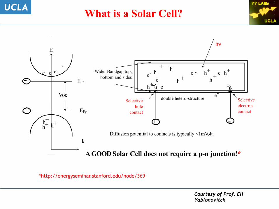
What is a Solar Cell?
Diffusion potential to contacts is typically <1mVolt. k
A GOOD Solar Cell does not require a p-n junction!*
hνE
EFn
EFp
Voc
e- h
h+ e-e-
e - h+ e- h+
e-
h+ +
h + h +Wider Bandgap top,
bottom and sides
double hetero-structure Selective electron contact
Selective hole
contact
+ -
-
+
e- e- e-
h+h+ h+
Courtesy of Prof. Eli Yablonovitch
*http://energyseminar.stanford.edu/node/369
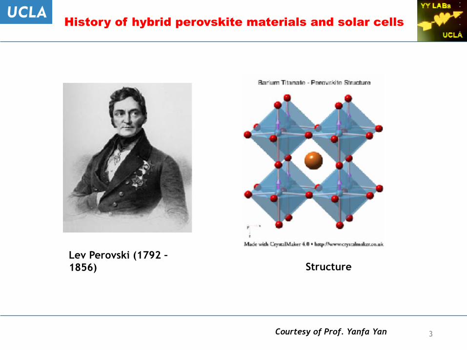
Lev Perovski (1792 – 1856) Structure
History of hybrid perovskite materials and solar cells
3Courtesy of Prof. Yanfa Yan

Perovskite Si CIGS GaAsBand gap (eV) 1.5 (tunable) 1.1 1.12 1.43
Absorption coefficient 104-5 103 104-5 104-5
Carrier mobility cm2/(V·s) 100 1500 < 10 8500
Carrier lifetime > 100 ns ms 50-200 ns <100 ns
Essential physical properties of major PV materials
Long Diffusion length
Low recombination rate
and high PL
Electron/hole transportation
Long carrier lifetime
4
Perovskite is a great PV material

Perovskite Si CIGS GaAsVOC 1.1 V 0.706 0.68V 1.12 V
VOC deficit 0.3 - 0.45 V 0.3-0.4V > 0.4 V ~0.3 V
JSC (mA/cm2) ~ 22 42.7 36 29.5FF ~80% ~ 80% ~80% >85%
Film thickness ~350 nm 100-200 um 1-2 um 4 um
Device parameters of different solar cells
5
Device parameter: A promising PV material
Yan et al, Adv. Mater. 2014, 26, 4653–4658

Planar Device structure: PiN & NiP
ITO
TiOx (N)
Perovskite (i)
Spiro (P)
Au
ITO
PEDOT or NiOx (P)
Perovskite (i)
PCBM or ZnO(N)
Au
N-i-P device structure (regular structure)
P-i-N device structure* (inverted structure)
At UCLA , we work on both PiN and NiP planar perovskite solar cells.
6
*Prof. T.F. Guo (Taiwan), (1) Adv. Mat. 25, 3727, 2013; (2) SPIE Solar and Alternative Energy, 2013
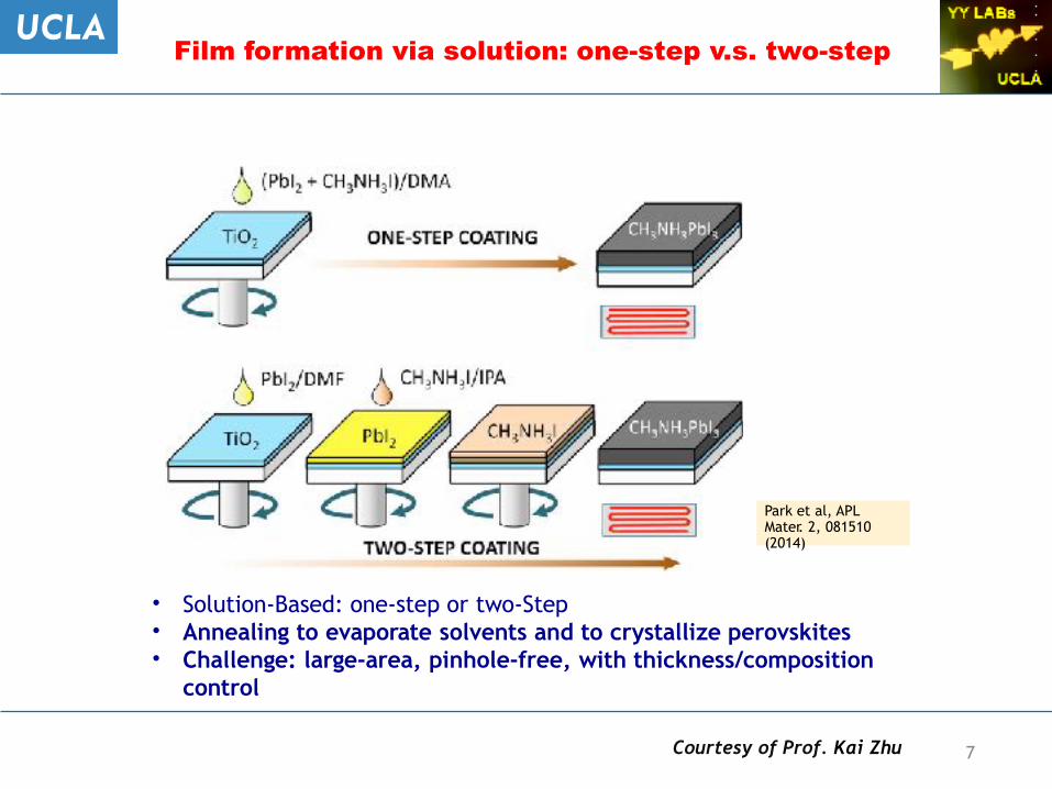
Park et al, APL Mater. 2, 081510 (2014)
• Solution-Based: one-step or two-Step • Annealing to evaporate solvents and to crystallize perovskites • Challenge: large-area, pinhole-free, with thickness/composition
control 10
Film formation via solution: one-step v.s. two-step
7Courtesy of Prof. Kai Zhu
8/16/17 8
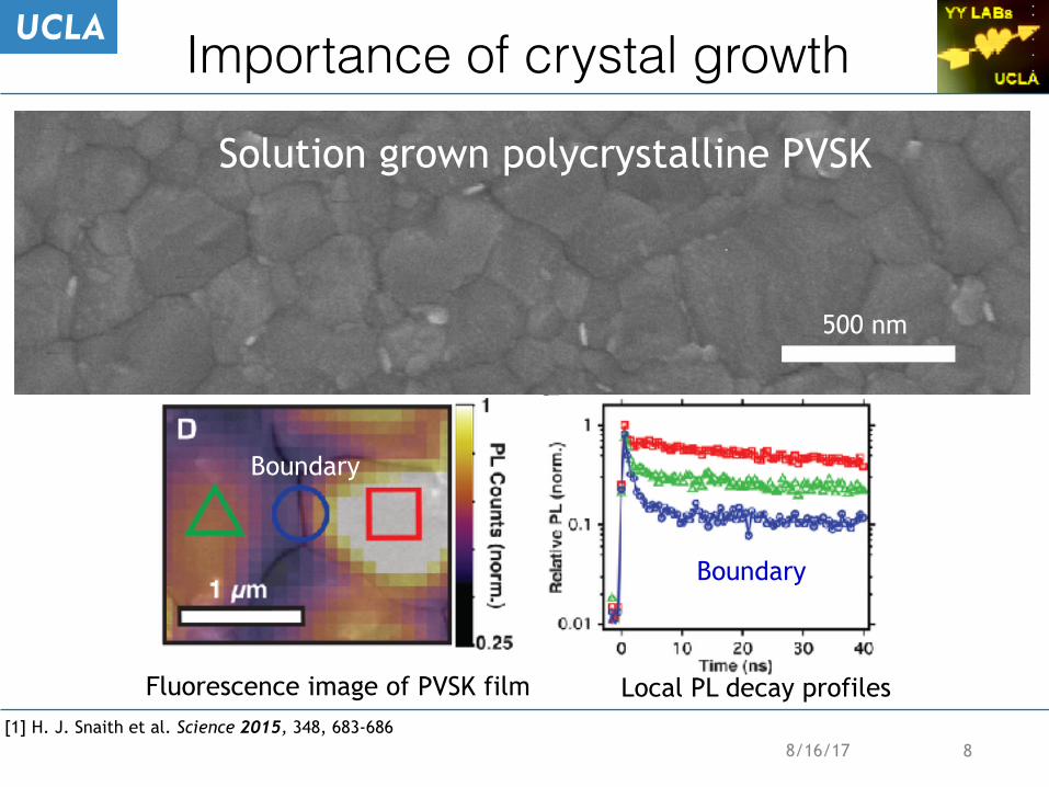
Importance of crystal growth
Solution grown polycrystalline PVSK
[1] H. J. Snaith et al. Science 2015, 348, 683-686
500 nm
Fluorescence image of PVSK film
Boundary
Boundary
Local PL decay profiles
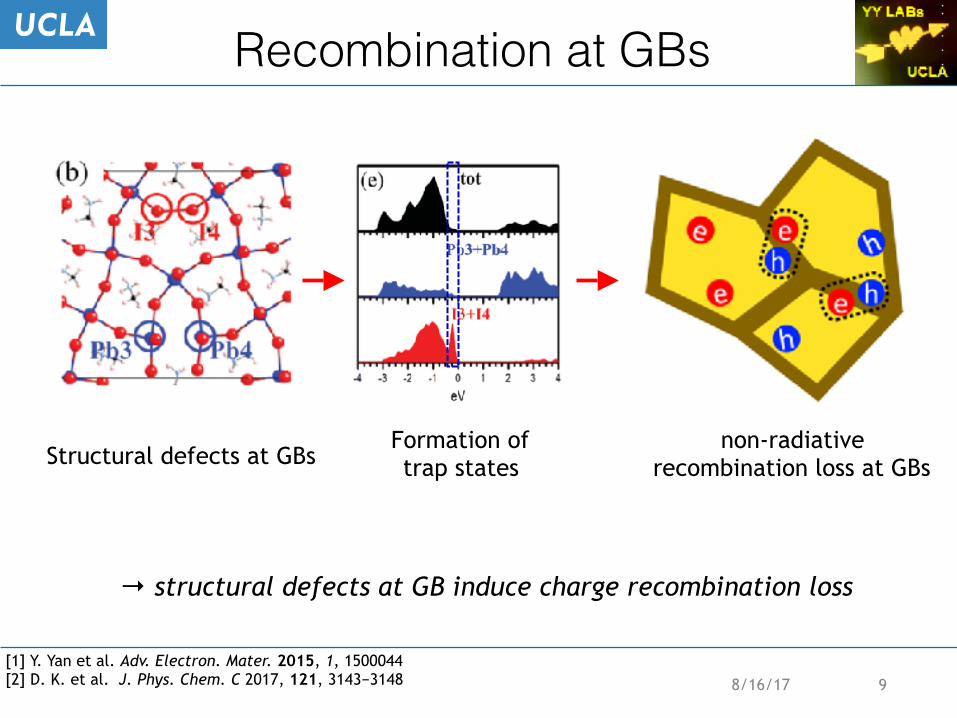
Recombination at GBs
Formation of trap statesStructural defects at GBs
non-radiative recombination loss at GBs
8/16/17 9
[1] Y. Yan et al. Adv. Electron. Mater. 2015, 1, 1500044 [2] D. K. et al. J. Phys. Chem. C 2017, 121, 3143−3148
→ structural defects at GB induce charge recombination loss
8/16/17 10
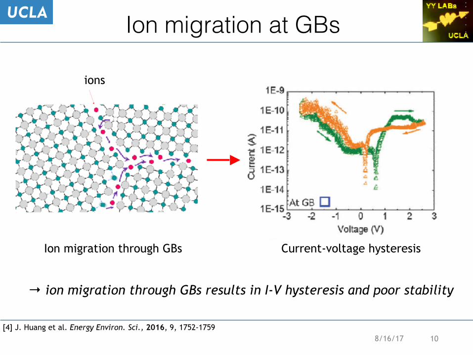
Ion migration through GBs Current-voltage hysteresis
Ion migration at GBs
ions
→ ion migration through GBs results in I-V hysteresis and poor stability
[4] J. Huang et al. Energy Environ. Sci., 2016, 9, 1752-1759
8/16/17 11
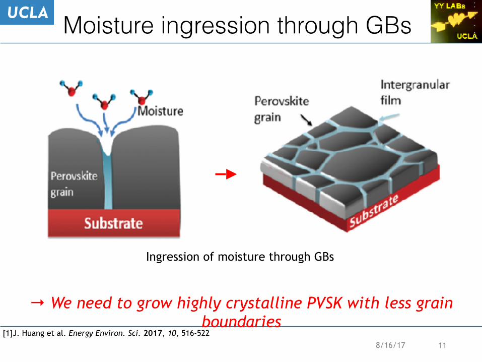
Ingression of moisture through GBs
Moisture ingression through GBs
→ We need to grow highly crystalline PVSK with less grain boundaries
[1]J. Huang et al. Energy Environ. Sci. 2017, 10, 516-522
8/16/17 12
1) Intermediate adduct method using a Lewis base additive
Manuscript under revision

Intermediate phase : adduct
8/16/17 13
MAPbI3
MAI•PbI2•DMSO MAI+PbI2+DMSO in DMF
After heatingIntermediate phase
X + :Y → X⋅Y acid base adduct
[1] N.-G. Park et al. J. Am. Chem. Soc. 2015, 137, 8696−8699 [2] N.-G. Park et al. Acc. Chem. Res. 2016, 49, 311−319
10 µm 10 µm
w/o intermediate phase w/ intermediate phase
DMSO (g)↑
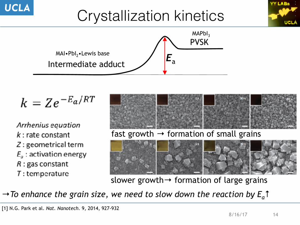
EaIntermediate adduct
PVSK
[1] N.G. Park et al. Nat. Nanotech. 9, 2014, 927-932
fast growth → formation of small grains
slower growth→ formation of large grains
Crystallization kinetics
→To enhance the grain size, we need to slow down the reaction by Ea↑
8/16/17 14
MAI•PbI2•Lewis base
MAPbI3

Urea additive for higher Ea
DMSO µ=3.96D
Urea µ=4.56D
···· ····
0 s 10 s 30 s 60 s 70 s 90 s 120 s
65 oC 100 oC
ref
w/ 10 mol% urea
MAI•PbI2•DMSO
MAI•PbI2•DMSO•urea0.1
σ-
σ+
σ-
σ+
→ stronger interaction of urea with PVSK precursor, Ea↑, k↓
8/16/17 15[1] Manuscript accepted.

ref 1 mol% 2 mol% 4 mol% 6 mol%14161820
PCE
(%)
0.6
0.7
0.8
FF
20
22
J SC (m
A/cm
2 )
1.0
1.1
1.2
V OC (V
)
0.0 0.2 0.4 0.6 0.8 1.0 1.20
5
10
15
20
25
RefJ
SC: 21.47 mA/cm2
VOC
: 1.048 VFF: 0.77PCE: 17.34%
w/ urea 4 mol%J
SC: 21.68 mA/cm2
VOC
: 1.092 VFF: 0.78PCE: 18.55%
Curre
nt d
ensit
y (m
A/cm
2 )
Voltage (V)
300 400 500 600 700 8000
20
40
60
80
100
EQE
(%)
Wavelength (nm)
Ref (20.91 mA/cm2) w/ 4 mol% urea (21.26 mA/cm2)
Effect of urea on PV performance
8/16/17 16[1] Manuscript accepted.
ref
w/ 4mol% urea
500 nm
ref
500 nm
w/ 4mol% urea
ITO+SnO2
PVSK
spiro-MeOTAD
Ag
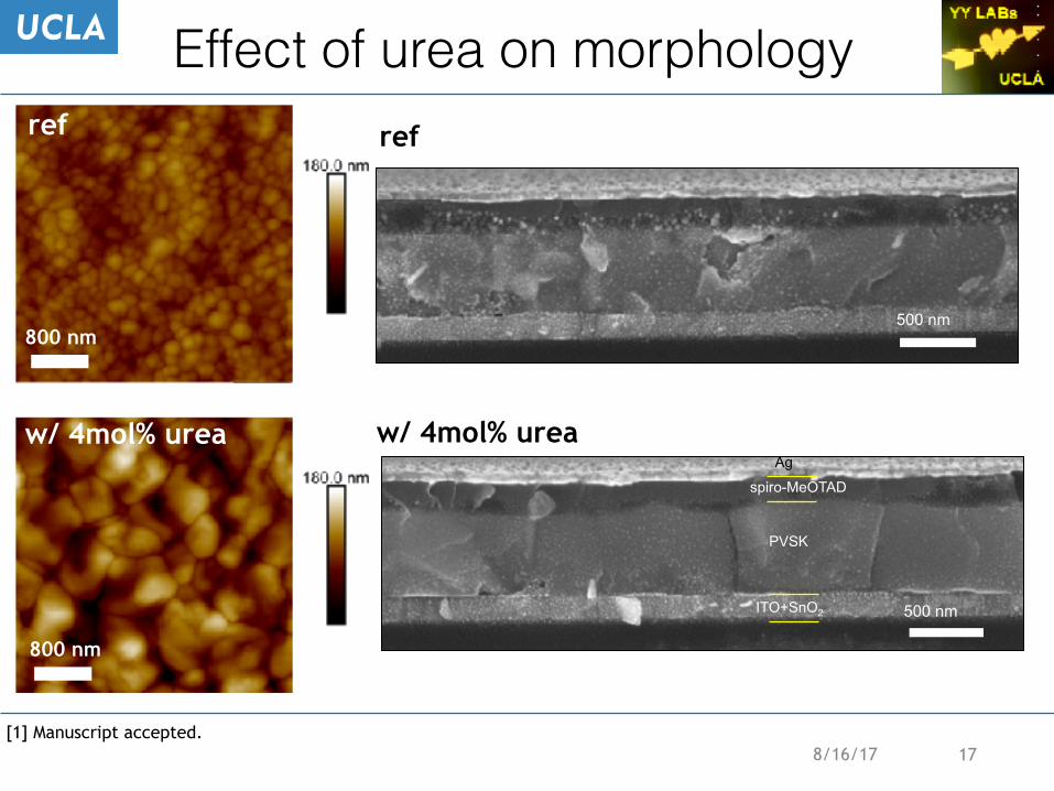
Effect of urea on morphology
8/16/17 17
800 nm
800 nm
[1] Manuscript accepted.
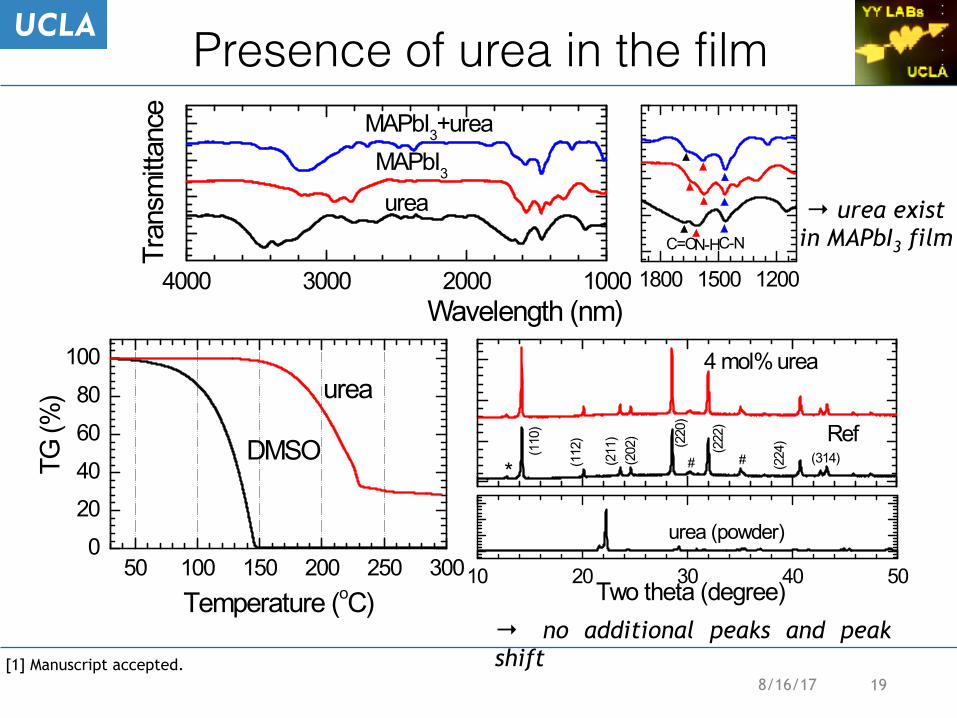
Presence of urea in the film
8/16/17 19
4000 3000 2000 1000
Tran
smitt
ance
Wavelength (nm)
MAPbI3+ureaMAPbI3urea
1800 1500 1200
C-NN-HC=O
10 20 30 40 50 Two theta (degree)
urea (powder)
# # (314)(224
)(222
)
(220
)
(202
)(2
11)
(112
)
4 mol% urea
Ref
(110
)
*
50 100 150 200 250 3000
2040
60
80
100urea
TG (%
)
Temperature (oC)
DMSO
→ urea exist in MAPbI3 film
→ no additional peaks and peak shift[1] Manuscript accepted.

8/16/17 20
Urea at GBPb I
ONC
A B C
D E F
4 mol% →with 50 mol% urea →crystallization of urea at GBs[1] Manuscript accepted.
8/16/17 21
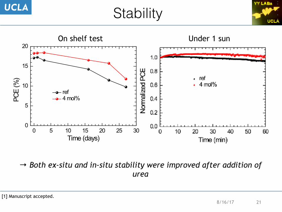
Stability
0 5 10 15 20 25 300
5
10
15
20
PCE
(%)
Time (days)
ref 4 mol%
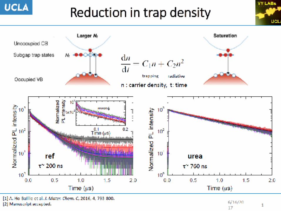
→ Both ex-situ and in-situ stability were improved after addition of urea
On shelf test Under 1 sun
[1] Manuscript accepted.
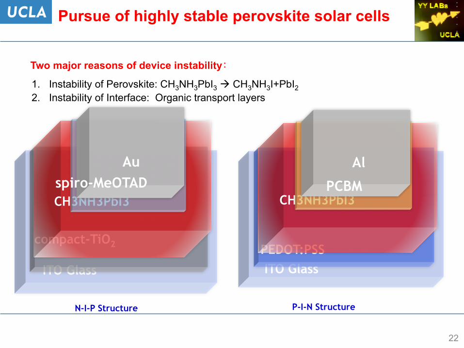
N-I-P Structure P-I-N Structure
1. Instability of Perovskite: CH3NH3PbI3 ! CH3NH3I+PbI2 2. Instability of Interface: Organic transport layers
Two major reasons of device instability:
Pursue of highly stable perovskite solar cells
ITO Glass
compact-TiO2
CH3NH3PbI3
Auspiro-MeOTAD
ITO GlassPEDOT:PSS
CH3NH3PbI3
Al
PCBM
22
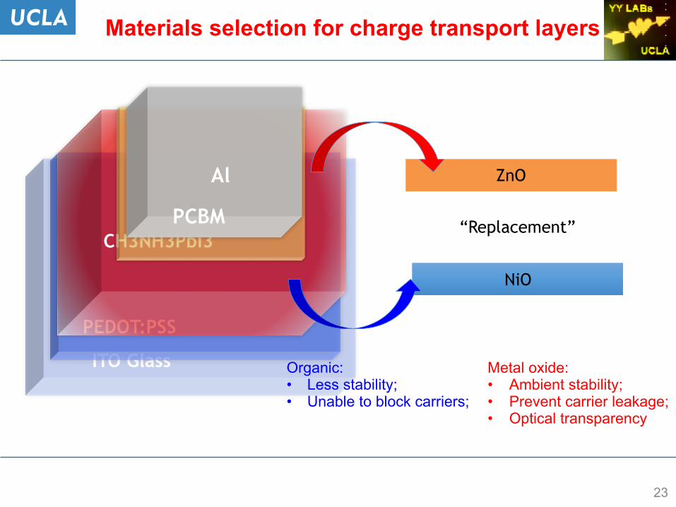
ITO Glass
PEDOT:PSS
CH3NH3PbI3
Al
PCBM
NiO
ZnO
Organic: • Less stability; • Unable to block carriers;
“Replacement”
Metal oxide: • Ambient stability; • Prevent carrier leakage; • Optical transparency
Materials selection for charge transport layers
23
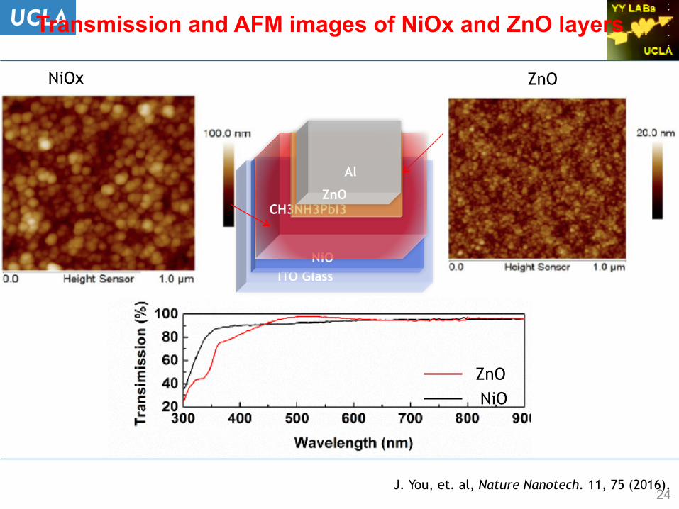
NiO
ITO Glass NiO
CH3NH3PbI3
Al
ZnO
ZnO
Transmission and AFM images of NiOx and ZnO layers
24J. You, et. al, Nature Nanotech. 11, 75 (2016).
NiOx ZnO

Device performance >16% PCE
Performance of Perovskite Solar Cells
25Y. Yang* et. al, Nature Nanotech. 11, 75 (2016).
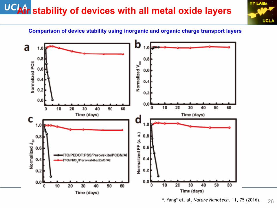
Comparison of device stability using inorganic and organic charge transport layers
Air stability of devices with all metal oxide layers
26Y. Yang* et. al, Nature Nanotech. 11, 75 (2016).
Summary & outlooks
27
1. We report our studies on (1) UCLA PVSK progress, (2) the intermediated phase engineering, (3) carrier transport layers (All metal oxides).
2. Many issues: physical mechanism(s), hysteresis, Pb-containing, water soluble, stability still require much more understanding
3. We are still in the early stage of the perovskite PV research, and we like to establish collaborations with others who are interested in this topic.
4. How about OPV? We are continuing to work on it, and please be patience, more ( and important) results to come.
Yang’s group, UCLA, summer 2016
Acknowledgments
Thank you for your attention
UC-Solar Program