Embed Size (px)
Citation preview

Solid State Ionics 135 (2000) 181–191www.elsevier.com/ locate / ssi
The crystal structural evolution of nano-Si anode caused by lithiuminsertion and extraction at room temperature
a a a , b b c*Hong Li , Xuejie Huang , Liquan Chen , Guangwen Zhou , Ze Zhang , Dapeng Yu ,d dYu Jun Mo , Ning Pei
aLab. for Solid State Ionics, Institute of Physics, Chinese Academy of Sciences, Beijing 100080, ChinabBeijing Laboratory of Electron Microscopy, Center for Condensed Matter Physics, Chinese Academy of Sciences, Beijing 100080,
ChinacDepartment of Physics, National Key Laboratory of Mesoscopic Physics, Peking University, Beijing 100871, China
dDepartment of Physics, Henan University, Kaifeng 475001, China
Abstract
The crystal structure and morphology of nanosized Si particles and wires after Li-insertion /extraction electrochemicallyhave been studied by ex-situ XRD, Raman spectroscopy and electronic microscopy. It is confirmed that the insertion oflithium ions at room temperature destroys the crystal structure of Si gradually and leads to the formation of metastableamorphous Li–Si alloy. Furthermore, local ordered structure of Si can be restored after the partial extraction of lithium ions,which indicates the extraction of lithium ions promoting the recrystallization of amorphous Li-inserted Si. It was alsoobserved that nanosized Si particles and wires were merged together after the insertion /extraction of lithium ions. 2000Elsevier Science B.V. All rights reserved.
Keywords: Nanosized Si; Lithium ion battery; Anode; Electrochemical insertion; Electron microscopy; Raman spectroscopy
1. Introduction Electrochemical alloying reaction of lithium withmetals has been widely studied since the 1970s
It has been reported that a large amount of lithium [2–8]. Previous studies revealed that Li can formions can be inserted into nanosized silicon by an various compounds with Si at elevated temperature,electrochemical method at room temperature [1]. such as Li Si , Li Si , Li Si and Li Si [5,8].12 7 13 4 7 3 22 5
Due to its high reversible capacity and better cyclic Recently, the structure variation of nanosized Siperformance, nanosized Si may be used as a novel particles (SiNPs) at heavy Li-insertion stateanode active material for lithium ion batteries. It has ( | Li Si) and partial Li-extraction state at room4
been suggested that the crystal structure of Si should temperature has been investigated by us using select-change with increasing dose of inserted lithium ions. ed area electron diffraction (SAED) [9]. SAED for
SiNPs in the Li-insertion state showed a dispersed-ring pattern. It indicates that the crystal structure of*Corresponding author. Tel.: 1 86-10-82649046; fax: 1 86-10-Si was destroyed due to the insertion of a large82649050.
E-mail address: [email protected] (L. Chen). amount of lithium ions leading to the formation of an
0167-2738/00/$ – see front matter 2000 Elsevier Science B.V. All rights reserved.PI I : S0167-2738( 00 )00362-3

182 H. Li et al. / Solid State Ionics 135 (2000) 181 –191
amorphous structure. SiNPs in partial the Li-ex- tween two stainless steel plates and cut into pieces2traction state showed a three-order ring pattern. The with area of 0.8 cm as SiNPs or SiNWs electrodes.
interplane spaces of the first, second and third order All cells were assembled and de-assembled in anrings are 0.198, 0.146 and 0.118 nm, respectively. It argon-filled glove box.may be related to new short-range ordered structures. The SiNPs and SiNWs electrode films for TEMHowever, the microstructure of Li-inserted nanosized observation were taken out from the cells afterSi and the evolution process of Si from crystal to electrochemical treatments. The sample powder wasamorphous structure are not very clear at that time. scratched from the Cu substrate and sealed in a glass
In this paper, the crystal structural evolution of Si tube containing anhydrous benzene in the glove box.including SiNPs and Si nanowires (SiNWs) has been After ultrasonic treatment, a droplet of benzenestudied in more detail by using further high-res- containing dispersed nano-Si particles was placed onolution transition electron microscopy (HRTEM) a copper grid covered with amorphous carbon film.combined with Raman spectroscopy. The morpholo- The Cu grid was sealed in a glass tube and taken outgy of SiNPs and SiNWs after the insertion /extraction from the glove box. Finally, the Cu grid wasof lithium ions has been investigated by scanning transferred into the vacuum chamber of the electronelectron microscopy (SEM) and TEM. microscope within 30 s. A JEOL –2010 transition
electron microscope operating at 200 kV was used toinvestigate the microstructure of SiNWs.
2. Experimental The morphology of SiNPs was observed by aHitachi S-4200 scanning electron microscope. The
Two types of nanosized Si powder were used in discharged or charged electrode films were taken outthis work. One is the ball-shape SiNPs, another is the from the cells and pasted directly onto a special shelfwire-like SiNWs. Pure SiNPs powder was prepared for SEM in the glove box, then sealed in a glassby laser-induced silane gas reaction [10]. The aver- bottle. During the transfer of the sample shelf fromage size of the Si particles are 80 nm, with a 20 nm the bottle into the vacuum chamber of the electrondistribution measured by a Zetasizer 3000 particle microscope, high pure argon gas flow was blownsize analytical instrument. SiNWs with a uniform onto the surface of the shelf continuously to mini-diameter distribution and high purity was synthesized mize the influence of moisture. The whole transferby laser ablation [11,12]. The average diameter of process was finished within several seconds.the SiNWs is about 15 nm and the length varies from The ex-situ Raman spectra were recorded by aa few tens to hundreds of micrometers. Each SiNWs Spex 1403 spectrophotometer with a 488.0 nm Ar-has a crystalline core and a thin surface layer of ion excitation line. A specially-designed optical cellamorphous silicon oxide (about 2 nm) [13]. was used. It has a quartz window and is vacuum-
The SiNPs and SiNWs samples at various lithium tight in order to avoid the interference of moistureinsertion /extraction states for TEM and SAED ob- during the test. The electrode films at differentservation were obtained by galvanostatic discharging discharged states were placed into the Raman cells inand charging a typical two-electrode cell to a differ- the glove box before the Raman test.ent voltage [14]. The cell was composed of a metallithium foil as a counter electrode, 1 M LiPF in a6
1:1 v/v mixture of ethylene carbonate (EC) and 3. Results and discussiondiethyl carbonate (DEC) as electrolyte, Celegard
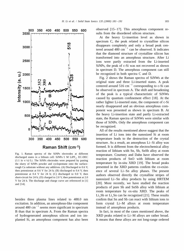
2300 as separator and nano-Si as a working elec- 3.1. Ex-situ Raman spectra of SiNPs and SiNWs attrode. The Nano-Si electrode was prepared by coat- different discharged statesing the binder-free slurry of SiNPs or SiNWs powderand cyclopentanone directly onto a surface-rough Ex-situ Raman spectra of the SiNPs electrode atcopper foil (0.018 mm in thickness, CARL Schlenk four Li-insertion levels are shown in Fig. 1. At theAG, German). The film was dried at 808C for 8 h lighter Li-insertion level, the Raman peak of c-Si at
6 21under vacuum, compressed under 1 3 10 Pa be- 518 cm can be observed in spectra A and B,
H. Li et al. / Solid State Ionics 135 (2000) 181 –191 183
observed [15–17]. This amorphous component re-sults from the disordered silicon structure.
At the heavy Li-insertion level as shown inspectrum C, the peak related to crystalline silicondisappears completely and only a broad peak cen-
21tered around 480 cm can be observed. It indicatesthat the diamond structure of crystalline silicon hastransformed into an amorphous structure. After Liions were partly extracted from the Li-insertedSiNPs, the peak of c-Si was not recovered as shownin spectrum D. The amorphous component can stillbe recognized in both spectra C and D.
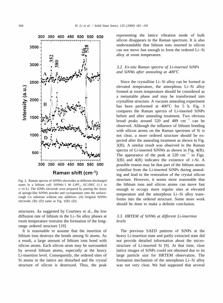
Fig. 2 shows the Raman spectra of SiNWs at theoriginal state and three Li-inserted states. A peak
21centered around 516 cm corresponding to c-Si canbe observed in spectrum A. The shift and broadeningof the peak is a typical characteristic of SiNWscaused by quantum confinement effect [18]. At therather lighter Li-inserted state, the component of c-Sinearly disappeared and an obvious amorphous com-ponent was presented as shown in spectrum B. Atthe heavy Li-insertion state and partly Li-extractedstate, the Raman spectra of SiNWs were similar withthose of SiNPs. Only the amorphous component canbe recognized.
All of the results mentioned above suggest that theinsertion of Li ions into the nanosized Si at roomtemperature leads to the destruction of the crystalstructure. As a result, an amorphous Li–Si alloy wasformed. It is different from the electrochemical alloyreaction of lithium with Sn, Sb, SnSb alloy at room
Fig. 1. Raman spectra of the SiNPs electrodes at different temperature. Courtney and Dahn have observed thedischarged states in a lithium cell: SiNPs/1 M LiPF , EC-DEC6 reaction products of SnO with lithium at room(1:1 in v/v) /Li. The SiNPs electrodes were prepared by pasting
temperature by in-situ XRD [19]. The broad peaksthe slurry of SiNPs powder and cyclopentane onto the surface-presented in the XRD patterns confirm the co-exist-rough Cu substrate without any additives. (A) Discharged to 0.6 V,
then potentiostat at 0.6 V for 24 h; (B) discharged to 0.4 V, then ence of several Li–Sn alloy phases. The presentpotentiostat at 0.4 V for 24 h; (C) discharged to 0.0 V, then authors observed directly the crystalline stripes ofshort-circuit for 24 h; (D) charged to 2.0 V, then potentiostat at 2.0
nanosized Li–Sn alloy products by using HRTEMV for 24 h. The discharge and charge curve are referenced in [1][20]. More recently, we have studied the reactionand [14].products of pure Sb and SnSb alloy with lithium atroom temperature by ex-situ XRD. The peaks ofLi Sb or Li Sn can be recognized [21]. These results3 x
besides three plasma lines related to 488.0 nm confirm that Sn and Sb can react with lithium ions toexcitation. In addition, an amorphous-like component form crystal Li–M alloys at room temperature
21around 480 cm seems more significant in spectrum instead of amorphous products.B than that in spectrum A. From the Raman spectra In fact, in most of the cases mentioned above, theof hydrogenerated amorphous silicon and ion im- XRD peaks related to Li–M alloys are rather broad.planted Si, an amorphous component has also been It means that these alloys are not long-range ordered
184 H. Li et al. / Solid State Ionics 135 (2000) 181 –191
representing the lattice vibration mode of bulksilicon disappears in the Raman spectrum. It is alsounderstandable that lithium ions inserted in siliconcan not move fast enough to form the ordered Li–Sialloy at room temperature.
3.2. Ex-situ Raman spectra of Li-inserted SiNPsand SiNWs after annealing at 4008C
Since the crystalline Li–Si alloy can be formed atelevated temperature, the amorphous Li–Si alloyformed at room temperature should be considered asa metastable phase and may be transformed intocrystalline structure. A vacuum annealing experimenthas been performed at 4008C for 5 h. Fig. 3compares the Raman spectra of Li-inserted SiNPsbefore and after annealing treatment. Two obvious
21broad peaks around 520 and 489 cm can beobserved. Although the influence of lithium bondingwith silicon atoms on the Raman spectrum of Si isnot clear, a more ordered structure should be ex-pected after the annealing treatment as shown in Fig.3(B). A similar result was observed in the Ramanspectra of Li-inserted SiNWs as shown in Fig. 4(B).
21The appearance of the peak at 520 cm in Figs.3(B) and 4(B) indicates the existence of c-Si. Apossible reason may be that part of the lithium atomsvolatilize from the Li-inserted SiNPs during anneal-ing and lead to the restoration of the crystal siliconstructure. However, it seems more reasonable thatFig. 2. Raman spectra of SiNWs electrodes at different dischargedthe lithium ions and silicon atoms can move faststates in a lithium cell: SiNWs/1 M LiPF , EC-DEC (1:1 in6
v /v) /Li. The SiNPs electrode were prepared by pasting the slurry enough to occupy more regular sites at elevatedof sponge-like SiNWs powder and cyclopentane onto the surface- temperature and the amorphous Li–Si alloy trans-rough Cu substrate without any additives. (A) Original SiNWs
forms into the ordered structure. Some more workelectrode, (B)–(D) same as Fig. 1(B)–(D).should be done to make a definite conclusion.
structures. As suggested by Courtney et al., the lowdiffusion rate of lithium in the Li–Sn alloy phases at 3.3. HRTEM of SiNWs at different Li-insertionroom temperature restrains the formation of the long- levelsrange ordered structure [19].
It is reasonable to assume that the insertion of The previous SAED patterns of SiNPs at thelithium ions destroys the bonds among Si atoms. As heavy Li-insertion state and partly extracted state dida result, a large amount of lithium ions bond with not provide detailed information about the micro-silicon atoms. Each silicon atom may be surrounded structure of Li-inserted Si [9]. At that time, clearby several lithium atoms, especially at the heavy lattice images of SiNPs could not obtained due to itsLi-insertion level. Consequently, the ordered sites of large particle size for HRTEM observation. TheSi atoms in the lattice are disturbed and the crystal formation mechanism of the amorphous Li–Si alloystructure of silicon is destroyed. Thus, the peak was not very clear. We had supposed that several

H. Li et al. / Solid State Ionics 135 (2000) 181 –191 185
Fig. 3. Raman spectra of Li-inserted SiNPs electrodes after annealing treatment. (A) The same as that in Fig. 1(C); (B) after step (A), thenvacuum-annealing at 4008C for 5 h. Dot line and solid line are fitting curves.
intermediate phases may be occurring with increas- and amorphous regions can be distinguished clearlying dose of inserted lithium [9]. from Fig. 5(B). The interplanar spacing for most
The microstructure of pure SiNWs has been crystal stripes is 0.31 nm corresponding to the h111jstudied by Yu and Lieber. The lattice images of plane of silicon. Thus, these crystal regions can beSiNWs were observed clearly using HRTEM [11– regarded as the unreacted part with lithium. It can be13]. Therefore, we used SiNWs as anode active seen that the amorphous region denoted by blackmaterials to investigate the crystal structure of arrows develops from the surface into the core ofSiNWs after electrochemical insertion. SiNWs. Due to the inhomogeneity of both electrical
Fig. 5(A)–(E) compares the HRTEM images of contact and the concentration distribution of lithiumSiNWs before and after Li-insertion. The image of a ions, the width of the amorphous regions is different.single SiNW is shown in Fig. 5(A) in which almost A few of the amorphous regions were also foundperfect (111) lattice fringes can be seen in the core within the crystalline matrix. This may be caused byregion. A thin amorphous layer is also observed on the penetration of lithium ions from the back of thethe surface of the SiNW. It is composed of silicon grain to the front. Furthermore, no new orderedoxide [11]. The thickness of the surface oxide layer structure can be seen near the interface between theof each SiNW is close to 2 nm. In fact, in most of crystal and amorphous regions. It indicates that thethe original SiNWs sample, abundant defaults also insertion of lithium ions destroys the crystal structurecoexist, such as microtwins, stacking faults and low- of Si directly instead of the formation of anyangle grain boundaries. intermediate phases.
Fig. 5(B) shows the image of SiNWs at the With an increasing dose of inserted lithium ions,shallow Li-insertion level. The crystalline Si core the amorphous regions develop further towards the

186 H. Li et al. / Solid State Ionics 135 (2000) 181 –191
Fig. 4. Raman spectra of the Li-inserted SiNWs electrode after annealing treatment. (A) The same as that in Fig. 2(C); (B) after step (A),then vacuum-annealing at 4008C for 5 h.
core part of a SiNW as shown in Fig. 5(C), resulting core part of SiNWs. The lattice spacing is about 0.31in further shrinking of the crystalline regions. It nm. It indicates that the amorphous Li–Si nanowirescould be observed that the original continuous recrystallize after extraction of part the lithium ions.crystalline region is divided into several slim stripes It has been known before that random crystallizationwithin the single SiNW. The dimension of these of pure amorphous silicon occurs above 6008C [22].stripes is reduced to a few nanometers. As a result, This indicates that the extraction of lithium ionsthe intensity of the photoluminescence spectra of promotes the nucleation and growth of Si in Li–SiLi-inserted SiNWs is increased significantly and the nanowires.band of light emission is blue-shifted obviously [14]. The electrochemical extraction of lithium ions
At the more heavy insertion level ( . Li Si), the from SiNWs or SiNPs was performed by charging a2.6
ordered Si lattice in a SiNW could disappear com- discharged cell of SiNWs/Li or SiNPs/Li to 2.0 Vpletely as shown in Fig. 5(D), indicating a full and keeping the potentiostat at 2.0 V for 24 h. It wastransformation from crystalline SiNWs into amor- found that a larger irreversible capacity loss alwaysphous Li–Si nanowires. exists [1]. According to the analysis on the dis-
Fig. 5(E) shows the image of three SiNWs after charge /charge curves of SiNPs/Li and SiNWs/Lilithium ions were partly extracted from the deeply cells, it is sure that the main part of the lost capacityinserted Li–Si nanowires. The crystalline regions is not caused by the decomposition reaction of thedenoted by white arrows can be seen clearly in the electrolyte. Based on the image of Fig. 5(E), Raman

H. Li et al. / Solid State Ionics 135 (2000) 181 –191 187
Fig. 5. The high resolution transmission electronic microscopy of SiNWs at different Li-insertion levels. (A) Original SiNWs, (B)–(E) afterthe same electrochemical treatment corresponding to Fig. 1(A)–(D), respectively.
spectra of Figs. 1(D) and 2(D), it can be concluded lithium ions under current electrochemical condi-that the amorphous component still exists at the tions. The remaining lithium ions may modify thecharged state. In fact, a large amount of intrinsic and crystal structure of nanosized Si and act as the maininsertion-generated defaults within the nanosized Si resource of irreversible capacity loss.can produce a lot of dangling bonds. Those dangling It can also be noticed that two SiNW denoted by 1bonds have a strong affinity to capture lithium ions. and 2 in Fig. 5(E) have merged together. SiNWWahl et al. has reported that substituted Li in Si can denoted by 3 seems to be hanging over SiNW 1.be kept stable at least up to 670 K [23]. Therefore, it Recently, we have found that the aggregation ofmay be very difficult to extract all the inserted nanosized active particles caused by electrochemical

188 H. Li et al. / Solid State Ionics 135 (2000) 181 –191
Fig. 5. (continued)
alloy reaction with lithium is a normal phenomenon transformation of the lattice structure could be[9,20,24]. It will be discussed in the following ignored.section.
Considering the result of Fig. 5, it can be deduced 3.4. Morphology variation of SiNPs and SiNWsthat the structure variation of nanosized Si from after Li-insertioncrystalline to amorphous and then back to crystallineis a reversible phase transformation. The influence of In fact, a large amount of merged SiNWs werethis variation on the electrochemical properties is not observed at both the deep discharged state andvery clear. Since a better cyclic performance of charged state from the images of HRTEM [25]. TheSiNPs can be achieved by adding a large amount of morphology variation of SiNPs caused by Li-inser-carbon black [1], it seems that the effect of the tion has also been investigated by SEM.

H. Li et al. / Solid State Ionics 135 (2000) 181 –191 189
Fig. 5. (continued)
Fig. 6(A) shows an image of the original SINPs SiNPs particles. It is obvious that the dense structureelectrode in which the SiNPs powder was mixed is not propitious to the insertion and extraction ofwith carbon black (CB) at a weight ratio of 1:1. The lithium ions in view of kinetics. In fact, although theaverage particle size of the ball-shape CB is 40 nm reversible capacity still fades with cycle number, the[25]. It can be seen that SiNPs particles are inter- cyclability of SiNPs adding with CB are much betterspersed among CB uniformly. However, when the than those without adding CB [1]. Therefore, it can
1SiNPs electrode was discharged to 0.0 V vs. Li /Li , be deduced that if serious agglomeration can bean obvious agglomeration can be seen in Fig. 6(B). restrained effectively, the cyclic performance will beA continuous net structure with many cavities or improved further. A recent study on a tin compositeholes was formed. From the zoom image as shown in oxide (TCO) anode also confirmed that the oxideFig. 6(C), it can be seen more clearly that many matrix can restrain the growth of nanosized Li–Sndispersed particles coalesce into a strong flocculation alloys [19,20]. Thus, a suitable inert matrix isstructure. In view of the morphology variation, this necessary to improve the electrochemical propertiesphenomenon can be named as electrochemical sinter- of nanosized alloy anodes.ing [26]. It should be emphasized that this type of agglome-
Fig. 6(D) and (E) show the images of the SiNPs ration force is very strong since each of the SiNWselectrode at a charged state after 20 cycles. The and SiNPs is covered by a silicon oxide layer with aagglomeration is more significant. The number of thickness of about 2 nm. A possible agglomerationcavities reduces further. mechanism is that the insertion of lithium ions
The morphology of the SiNPs electrode without expands the volume of each particle and increasesCB at a charged state has been investigated by us the contact probability of separated particles. Due to[9]. A typical view of them is shown in Fig. 6(F). the high surface energy of nanosized particles [27], itThe separated SiNPs particles have agglomerated is beneficial to decrease the surface energy byinto very dense blocks denoted by a black arrow (the merging. Especially when lithium ions bonded withregion denoted by a white arrow is the surface-rough surface Si atoms are extracted from the surfaceCu substrate). The width of each block is over regions of SiNWs or SiNPs by the electrochemicalseveral micrometers. Comparing Fig. 6(F) with Fig. method, those Si atoms of neighbor particles may6(D) and (E), indicates that carbon black at this case have a strong affinity to bond together and form andoes not restrain effectively the agglomeration of agglomerated body.

190 H. Li et al. / Solid State Ionics 135 (2000) 181 –191
Fig. 6. The scanning electronic micrographs of the SiNPs electrode at different discharged states (A) original SiNPs electrode prepared by amixture of SiNPs powder, carbon black and PVDF at a weight ratio of 4:4:2. (B) SiNPs electrode after the same electrochemical treatmentas that described in Fig. 1(C). (C) Zoom part of Fig. 6(B). (D) SiNPs electrode after the same electrochemical treatment with Fig. 1(D). (E)Zoom part of Fig. 6(D). (F) A pure SiNPs electrode after the same electrochemical treatment with Fig. 1(D), the electrode was prepared inthe same way as that described in the caption of Fig. 1.

H. Li et al. / Solid State Ionics 135 (2000) 181 –191 191
[6] R.N. Seefurth, R.A. Sharma, J. Electrochem. Soc. 1244. Conclusions(1977) 1207.
[7] B.A. Boukamp, G.C. Lesh, R.A. Huggins, J. Electrochem.The electrochemical insertion of lithium ions at Soc. 128 (1981) 725.
room temperature destroys directly the crystal struc- [8] K. Amezawa, N. Yamamoto, Y. Tomii, Y. Ito, J. Electrochem.ture of Si leading to the formation of the metastable Soc. 145 (1998) 1986.
[9] H. Li, X.J. Huang, L.Q. Chen, J.Q. Li, Y.Q. Zhou, Z.G. Wu,amorphous Li–Si alloy. After the extraction ofY. Liang, (submitted).partial lithium ions electrochemically, a local ordered
[10] Y. Li, Y. Liang, K. Xiao, F. Zheng, Z. Hu, Acta Meta. Sinicastructure can be obtained. The extraction of lithium 31 (1995) B21.ions promotes the recrystallization of amorphous [11] D.P. Yu, C.S. Lee, I. Bello, X.S. Sun, Y.H. Tang, G.W. Zhou,Li-inserted Si at room temperature. This order–disor- Z.G. Bai, Z. Zhang, S.Q. Feng, Solid State Commun. 105
(1998) 403.der transition is reversible. It is not easy to extract all[12] A.M. Morales, C.M. Lieber, Science 279 (1998) 208.inserted lithium ions from nanosized Si by the[13] G.W. Zhou, Z. Zhang, Z.G. Bai, S.Q. Feng, D.P. Yu, Appl.
electrochemical method. Some lithium ions may be Phys. Lett. 73 (1998) 677.captured by unsaturated Si atoms resulting in the [14] H. Li, G.W. Zhou, D.P. Yu, X.J. Huang, L.Q. Chen, Z. Zhang,irreversible capacity loss. The nanosized Si particles Appl. Phys. Lett. 75 (1999) 2447.
[15] Z. Iqbal, S. Veprek, J. Phys. C.: Solid State Phys. 15 (1982)have a strong tendency to merge together during the377.process of insertion /extraction of lithium ions.
[16] T. Motooka, O.W. Holland, Appl. Phys. Lett. 61 (1992)3005.
[17] T. Motooka, O.W. Holland, Appl. Phys. Lett. 58 (1991)Acknowledgements 2360.
[18] B.B. Li, D.P. Yu, S.L. Zhang, Phys. Rev. B 59 (1999) 1645.[19] I.A. Courtney, J.R. Dahn, J. Electrochem. Soc. 144 (1996)This work was supported by Ford-NSFC Founda-
2045.tion (contact No. 9712304), NSFC (contact No. [20] H. Li, X.J. Huang, L.Q. Chen, Electrochem. Solid State Lett.59972041 and 19774022) and National 863 Key 1 (1998) 241.Program (contact No. 715-004-0280). [21] H. Li, G.Y. Zhu, X.J. Huang, L.Q. Chen, J. Mater. Chem.
2000, in press.[22] T.D. Chen, C.C. Koch, T.L. Mccormick, R.J. Nemanich, J.Y.
Huang, J.G. Huang, J. Mater. Res. 10 (1995) 139.References [23] W. Wahl, H. Hofsaaa, S.G. Hahn, S. Winter, E. Recknagei,
Appl. Phys. Lett. 62 (1993) 684.[1] H. Li, X.J. Huang, L.Q. Chen, Z.G. Wu, Y. Liang, Electro- [24] H. Li, L.H. Shi, W. Lu, X.J. Huang, L.Q. Chen (submitted).
chem. Solid State Lett. 2 (1999) 547. [25] Hong Li, unpublished data.[2] S. Lai, J. Electrochem. Soc. 123 (1976) 1196. [26] J.T. Vaughey, K.D. Keplar, D.R. Vissers, M.M. Thackeray,[3] R.A. Sharma, R.N. Seefurth, J. Electrochem. Soc. 123 Abstracts of the 9th International Meeting on Lithium
(1976) 1763. Batteries, Edinburgh, Scotland, July, 1998, Poster I, Tues 82.[4] R.N. Seefurth, R.A. Sharma, J. Electrochem. Soc. 127 [27] N. Ichinose, Y. Ozaki, S. Kashu (Eds.), Superfine Particle
(1980) 1101. Technology, Springer–Verlag, London, 1992, p. 13.[5] C.J. Wen, R.A. Huggins, J. Solid State Chem. 37 (1976) 271.