Embed Size (px)
Citation preview
5
The Composite Structure of Hologram and Optical Waveguide
Renxi Gao and Wenjun Liu Harbin institute of technology at weihai, Weihai
China
1. Introduction
Optical holography is an excellent technology which can be applied in many fields, such as
3D-displays, information storage, products packaging, interferometer survey, optical
connection and computer and so on. The conventional holography include reference wave,
object wave and diffracting wave. These optical waves are spatial light and the whole
hologram set up is fair size. The optical waveguides which are set up in optical routs can be
integrated into a mini-chip. A new class of holography is proposed by many researchers
[Suhara, et al., 1976; Putilin, et al., 1991; Singher & Shamir, 1994], in which the evanescent
part of a guided wave or the guided wave in a waveguide is utilized as the reference wave
or the illuminating one. This kind of hologram is defined as “waveguide hologram”, and it
has significant advantages in integration, wide field of view, compactness and other special
functions. In this chapter, three sections are used to introduce the new development of
waveguide hologram in the optical memory, optical connection and see-through planar
displays fields.
2. The multilayered waveguides and holograms structure (MWH) for memory
With the development of information era, the dramatic increasing of information data needs
new technologies of high density data storage. The holographic storage is regarded as a
promising candidate for the next generation of optical memory. However, the conventional
reconstructed holographic system includes reference wave and diffracting wave, which are
spatial lights. The whole hologram system devices are large, so they are not suitable for
personal use. The commercially available optical compact disc (CD) products have many
advantages and play a key role in data storage area. But the data density of the optical disc
can be hardly increased. We also know that the waveguide holography offers many
advantages compared with conventional holograms. Waveguide holograms provide
capability for the recording and reconstructing of holographic images or data information
with light which propagates along optical waveguides. A higher image-to-background
contrast and diffraction efficiency can be obtained because the direction of diffracted light
wave is vertical to the illuminating light wave. Furthermore, waveguide holograms provide
minimized illumination space and obstruction-free viewing. Therefore, multilayered
waveguide and hologram technology is a promising candidate to solve the problems for the
www.intechopen.com
Holography, Research and Technologies
110
next generation of optical data storage systems, many researchers have focused on this
work[Imai, et al.,2003; Ishihara, et al., 2004; Mitasaki & Senda, 2006; Yagi, et al., 2007; Yagi,
et al., 2008 ].
2.1 The principle of multilayered waveguide hologram memory
At present, there are many types of multilayered waveguide hologram structure. In this
chapter, only three main types of multilayered waveguide structure for optical data storage
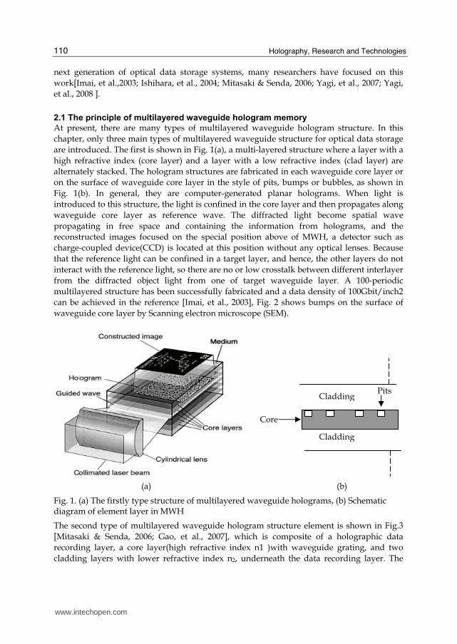
are introduced. The first is shown in Fig. 1(a), a multi-layered structure where a layer with a
high refractive index (core layer) and a layer with a low refractive index (clad layer) are
alternately stacked. The hologram structures are fabricated in each waveguide core layer or
on the surface of waveguide core layer in the style of pits, bumps or bubbles, as shown in
Fig. 1(b). In general, they are computer-generated planar holograms. When light is
introduced to this structure, the light is confined in the core layer and then propagates along
waveguide core layer as reference wave. The diffracted light become spatial wave
propagating in free space and containing the information from holograms, and the
reconstructed images focused on the special position above of MWH, a detector such as
charge-coupled device(CCD) is located at this position without any optical lenses. Because
that the reference light can be confined in a target layer, and hence, the other layers do not
interact with the reference light, so there are no or low crosstalk between different interlayer
from the diffracted object light from one of target waveguide layer. A 100-periodic
multilayered structure has been successfully fabricated and a data density of 100Gbit/inch2
can be achieved in the reference [Imai, et al., 2003], Fig. 2 shows bumps on the surface of
waveguide core layer by Scanning electron microscope (SEM).
(a) (b)
Fig. 1. (a) The firstly type structure of multilayered waveguide holograms, (b) Schematic diagram of element layer in MWH
The second type of multilayered waveguide hologram structure element is shown in Fig.3
[Mitasaki & Senda, 2006; Gao, et al., 2007], which is composite of a holographic data
recording layer, a core layer(high refractive index n1 )with waveguide grating, and two
cladding layers with lower refractive index n2, underneath the data recording layer. The
Cladding
Cladding
Core
Pits
www.intechopen.com
The Composite Structure of Hologram and Optical Waveguide
111
light was coupled into the waveguide core at the edge of MWH by cylindrical lens and then
excited guide-mode light which propagated along the waveguide core. When meeting the
waveguide gratings, the guide-mode light are diffracted into free space light as reference
wave of holographic data recording layer. When the hologram recording layer is
illuminated with these reference waves, the data information or holographic image is
reconstructed by diffracted light of hologram recording layer. The direction of diffracted
light of waveguide gratings can be different for each layers, thus the angle of β of light can
be changed according to the structure of waveguide gratings for each layer. This type MHW
also can be applied in three-dimension displays when many waveguides layers are
illuminated at the same time.
Fig. 2. SEM micrograph of a waveguide hologram (Imai, et al., 2003)
Fig. 3. Another type structure of multilayered waveguide holography element
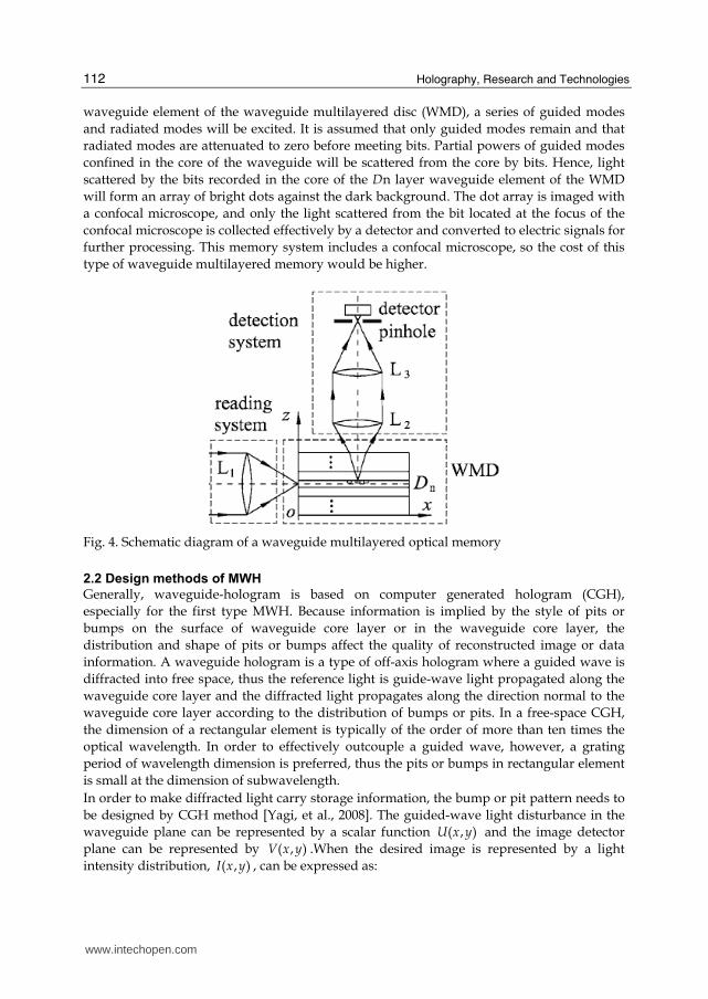
Until now, we just discuss the type of MWH memory in which diffracted lights are coherent
ly interfered. Guo et al. proposed a waveguide multilayered optical memory (WMOM) with
bits stored as a refractive index change [Guo, et al., 2007], such as in Fig.4. The principle of
reading data from a WMOM is based on scattering light from waveguide defects. In Fig. 4,
when the incident light is coupled by the reading system L1 into the core of the nth- Dn layer
Clad
Hologram
Gratings
Clad
Core
β
n2
n1
www.intechopen.com
Holography, Research and Technologies
112
waveguide element of the waveguide multilayered disc (WMD), a series of guided modes
and radiated modes will be excited. It is assumed that only guided modes remain and that
radiated modes are attenuated to zero before meeting bits. Partial powers of guided modes
confined in the core of the waveguide will be scattered from the core by bits. Hence, light
scattered by the bits recorded in the core of the Dn layer waveguide element of the WMD
will form an array of bright dots against the dark background. The dot array is imaged with
a confocal microscope, and only the light scattered from the bit located at the focus of the
confocal microscope is collected effectively by a detector and converted to electric signals for
further processing. This memory system includes a confocal microscope, so the cost of this
type of waveguide multilayered memory would be higher.
Fig. 4. Schematic diagram of a waveguide multilayered optical memory
2.2 Design methods of MWH
Generally, waveguide-hologram is based on computer generated hologram (CGH),
especially for the first type MWH. Because information is implied by the style of pits or
bumps on the surface of waveguide core layer or in the waveguide core layer, the
distribution and shape of pits or bumps affect the quality of reconstructed image or data
information. A waveguide hologram is a type of off-axis hologram where a guided wave is
diffracted into free space, thus the reference light is guide-wave light propagated along the
waveguide core layer and the diffracted light propagates along the direction normal to the
waveguide core layer according to the distribution of bumps or pits. In a free-space CGH,
the dimension of a rectangular element is typically of the order of more than ten times the
optical wavelength. In order to effectively outcouple a guided wave, however, a grating
period of wavelength dimension is preferred, thus the pits or bumps in rectangular element
is small at the dimension of subwavelength.
In order to make diffracted light carry storage information, the bump or pit pattern needs to
be designed by CGH method [Yagi, et al., 2008]. The guided-wave light disturbance in the
waveguide plane can be represented by a scalar function ( , )U x y and the image detector
plane can be represented by ( , )V x y .When the desired image is represented by a light
intensity distribution, ( , )I x y , can be expressed as:
www.intechopen.com
The Composite Structure of Hologram and Optical Waveguide
113
2
( , ) ( , )I x y V x y= (1)
Because of the image detector parallel to the waveguide, then the relations is
( , ) ( , ) ( , )V x y G x y U x y d dξ η ξ η= − −∫∫ (2)
Where G is a weight diffracted function such that
2 2 2
2 2 2
exp( )jk x y dA
x y d
+ ++ + (3)
Here d is the distance between the plane of image detector and the waveguide storage layer.
A is a constant. As V(x, y) is a convolution of U(x, y) and G(x, y), we can obtain U(x, y) for a
given V(x, y) by Fourier-transform calculations. The next step involves finding a way to
modulate the bump pattern and thus generate a light, represented by U(x, y), from the
guided wave. The area of the bump pattern can be divided into minute square cells whose
size at the level of micrometer. The above calculations are performed with sampling at this
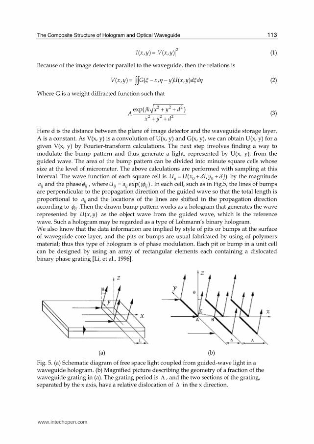
interval. The wave function of each square cell is 0 0( , )ijU U x i y jδ δ= + + by the magnitude
ija and the phase ijφ , where exp( )ij ij ijU a jφ= . In each cell, such as in Fig.5, the lines of bumps
are perpendicular to the propagation direction of the guided wave so that the total length is
proportional to ija and the locations of the lines are shifted in the propagation direction
according to ijφ .Then the drawn bump pattern works as a hologram that generates the wave
represented by ( , )U x y as the object wave from the guided wave, which is the reference
wave. Such a hologram may be regarded as a type of Lohmann’s binary hologram. We also know that the data information are implied by style of pits or bumps at the surface
of waveguide core layer, and the pits or bumps are usual fabricated by using of polymers
material; thus this type of hologram is of phase modulation. Each pit or bump in a unit cell
can be designed by using an array of rectangular elements each containing a dislocated
binary phase grating [Li, et al., 1996].
(a) (b)
Fig. 5. (a) Schematic diagram of free space light coupled from guided-wave light in a waveguide hologram. (b) Magnified picture describing the geometry of a fraction of the waveguide grating in (a). The grating period is Λ , and the two sections of the grating, separated by the x axis, have a relative dislocation of Δ in the x direction.
www.intechopen.com
Holography, Research and Technologies
114
The phase-matching condition must be fulfilled between the guided wave and the radiation wave:
0 02 / sin 0, 1, 2,effn k m nk mπ θ+ Λ = = ± ± ⋅ ⋅ ⋅ (4)
Where effn is the effective refractive index of guided-wave and n is the refractive index of
the material within which the diffracted light propagates, θ is the radiation angle with
respect to the normal of waveguide, such as in Fig. 5(a). 0 02 /k π λ= and 0λ is the free-space
wavelength. M is the order of diffraction. In order to increase the output efficiency of
diffracted light, only the -1st diffraction order satisfies the equation (4) when m= -
1.Therefore, the grating period Λ (the unit cell size) must satisfy,
0 0/ effnλ λ≤ Λ < (5)
In Fig. 5(b), the unit cell is divided into two sections. Each section of the grating acts
independently as an outcoupler, and the grating grooves in the two sections are relatively
dislocated by a distance Δ along the guided wave propagating direction u. The grating
period (Λ ) satisfies (5). According to Fig. 5(b), there is an optical path difference, Lδ ,
between the radiation light outcoupled by two sections of the grating, which can be
expressed as
( sin )
eff
eff
L n AB nAC
n n
δθ
= −= − Δ (6)
Taking into equation of (4) and noting that m= -1, the phase difference between the
diffracted light,δφ , as
0= 2 /k Lδφ δ π= Δ Λ (7)
It shows that a phase shiftδφ can be introduced by a grating dislocation Δ , and there exists
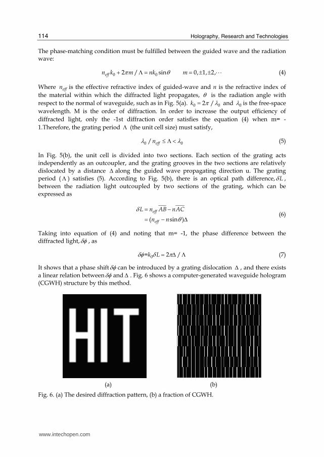
a linear relation betweenδφ and Δ . Fig. 6 shows a computer-generated waveguide hologram
(CGWH) structure by this method.
(a) (b)
Fig. 6. (a) The desired diffraction pattern, (b) a fraction of CGWH.
www.intechopen.com
The Composite Structure of Hologram and Optical Waveguide
115
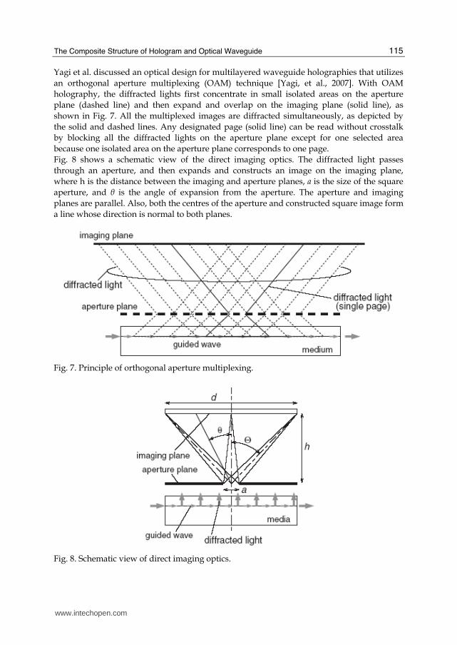
Yagi et al. discussed an optical design for multilayered waveguide holographies that utilizes
an orthogonal aperture multiplexing (OAM) technique [Yagi, et al., 2007]. With OAM
holography, the diffracted lights first concentrate in small isolated areas on the aperture
plane (dashed line) and then expand and overlap on the imaging plane (solid line), as
shown in Fig. 7. All the multiplexed images are diffracted simultaneously, as depicted by
the solid and dashed lines. Any designated page (solid line) can be read without crosstalk
by blocking all the diffracted lights on the aperture plane except for one selected area
because one isolated area on the aperture plane corresponds to one page.
Fig. 8 shows a schematic view of the direct imaging optics. The diffracted light passes
through an aperture, and then expands and constructs an image on the imaging plane,
where h is the distance between the imaging and aperture planes, a is the size of the square
aperture, and θ is the angle of expansion from the aperture. The aperture and imaging
planes are parallel. Also, both the centres of the aperture and constructed square image form
a line whose direction is normal to both planes.
Fig. 7. Principle of orthogonal aperture multiplexing.
Fig. 8. Schematic view of direct imaging optics.
www.intechopen.com
Holography, Research and Technologies
116
They discussed two types of optical design for OAM installed waveguide holograms. Both
types can eliminate the need for an active focusing servo for imaging optics. The direct
imaging optics offers a thinner driver, but it has a lower bit density and a shorter
wavelength margin than the telecentric imaging optics. On the other hand, the telecentric
imaging optics requires a thicker driver, but it offers a three fold higher bit density and a
longer wavelength margin than the direct imaging optics.
2.3 Fabrication process of MWH
A multilayered waveguide hologram consists of a stack of single-mode slab waveguides
with polymer as the main materials. So the fabrication methods of MWH are mainly
concerned with the processing of polymer optical waveguides and the holograms. The size
of pits or bumps of hologram designed by computer-generated hologram is small in
dimension of subwavelength, so it is necessary to use the high precision micro-fabricating
technology, such as photoresist-based patterning, direct lithographic patterning, soft
lithography, embossing process and so on. In this section, we only introduce some key
fabricating technologies for MWH.
• Spin-coating technology Spin coating is an effective method to fabricate multilayered films with different thickness.
We also know that the element of MHW is consist of the waveguide core layer with high
refractive index of material and cladding layer with low refractive index of material. In this
case, the substrate (rigid glass or flexible polyimide film) is mounted horizontally on a
rotating platform. The substrate then spins very rapidly and the coating solution is
dispensed onto it. The high-speed rotation throws off most of the solution, leaving behind a
thin, uniform coating. Film thickness is precisely controlled by the rotational speed of the
substrate. Faster rotation results in a thinner waveguide film layer. It is easy to form the film
with thickness of 1~100┤m by this method. However, Spin coating technology must be
combined with other micro-manufacturing technology (such as photoresist patterning,
reactive ion etching) to process computer-generated waveguide hologram.
• Lithographic patterning Lithography is playing a critical role in micro- and nano-fabricated patterns for
semiconductor devices and optics devices. It also can be adapted to process bits or bumps
patterns on the surface of waveguide core layer in the computer-generated hologram. The
techniques that can be used for patterning MWH included photoresist-based patterning,
direct lithographic patterning, and soft lithography. The technology of photoresist-based
patterning is seldom applied in fabrication of MWH, because that it needs cleaner room and
reactive ion etching process, thus the cost of MWH is higher that other lithography
patterning technology.
The direct laser lithography is a useful technique to fabricate a large planar areas with
precision patterns, and it has the advantage of being maskless, allowing rapid and
inexpensive prototyping in contrast to conventional mask-based photolithographic
approaches. Mitasaki et al. proposed a write-once recording technique for MHW cards by
laser directly writing, which can be suitable to record individual data easily in each MWH
card [Mitasaki et al., 2006]. Soft lithography is a micro-fabrication technique that has been
shown to generate high quality micro and nanostructures. It eliminates the use of costly and
time consuming lithographic techniques and equipment. Unlike photolithography, it has
www.intechopen.com
The Composite Structure of Hologram and Optical Waveguide
117
flexibility in material selection, can be applied to large planar surfaces, and provided high
precise control over chemistry of patterned surfaces. Some of the diverse fabrication
methods known collectively as soft lithography include: replica molding, micromolding in
capillaries, microcontact printing, and microtransfer molding.
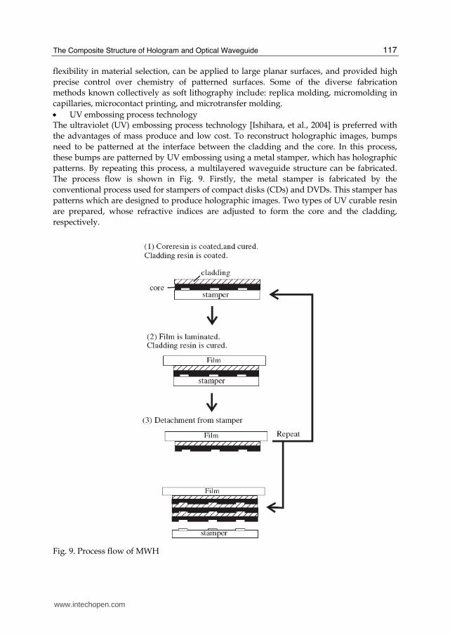
• UV embossing process technology The ultraviolet (UV) embossing process technology [Ishihara, et al., 2004] is preferred with
the advantages of mass produce and low cost. To reconstruct holographic images, bumps
need to be patterned at the interface between the cladding and the core. In this process,
these bumps are patterned by UV embossing using a metal stamper, which has holographic
patterns. By repeating this process, a multilayered waveguide structure can be fabricated.
The process flow is shown in Fig. 9. Firstly, the metal stamper is fabricated by the
conventional process used for stampers of compact disks (CDs) and DVDs. This stamper has
patterns which are designed to produce holographic images. Two types of UV curable resin
are prepared, whose refractive indices are adjusted to form the core and the cladding,
respectively.
Fig. 9. Process flow of MWH
www.intechopen.com
Holography, Research and Technologies
118
On the metal stamper, the UV curable resin for the core is spin-coated and UV-cured. Next,
the UV curable resin for the cladding is spin-coated. A plastic film is laminated on it. After
the resin is UV-cured, the film/cladding/core structure is detached from the metal stamper.
By this process, the patterns of the metal stamper are replicated on the core layer surface.
This process is repeated until the designated number of layers is fabricated. From the second
cycle, the detached structure at the end of the former cycle is laminated instead of the plastic
film, as shown in Fig. 9.
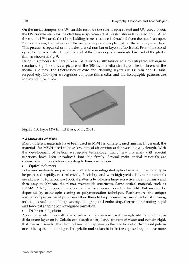
Using this process, Ishihara K. et al. have successfully fabricated a multilayered waveguide
structure. Fig. 10 shows a picture of the 100-layer media structure. The thickness of the
media is 2 mm. The thicknesses of core and cladding layers are 1.6 mm and 11 mm,
respectively. 100-layer waveguides compose this media, and the holographic patterns are
replicated in each layer.
Fig. 10. 100 layer MWH , [Ishihara, et al., 2004].
2.4 Materials of MWH
Many different materials have been used in MWH in different mechanisms. In general, the
materials for MWH need to have low optical absorption at the working wavelength. With
the development of optical waveguide technology, many new materials with special
functions have been introduced into this family. Several main optical materials are
summarized in this section according to their mechanism.
• Optical polymers Polymeric materials are particularly attractive in integrated optics because of their ability to
be processed rapidly, cost-effectively, flexibility, and with high yields. Polymeric materials
are allowed to form compact optical patterns by offering large refractive index contrasts and
then easy to fabricate the planar waveguide structures. Some optical material, such as
PMMA, PDMS, Epoxy resin and so on, now have been adopted in this field.. Polymer can be
deposited by using spin coating or polymerization technique. Furthermore, the unique
mechanical properties of polymers allow them to be processed by unconventional forming
techniques such as molding, casting, stamping and embossing, therefore permitting rapid
and low-cost shaping for waveguide formation.
• Dichromated gelatin A normal gelatin film with less sensitive to light is sensitized through adding ammonium
dichromate layer on it. Gelatin can absorb a very large amount of water and remain rigid,
that means it swells. The chemical reaction happens on the interface of dichromated gelatin
once it is exposed under light. The gelatin molecular chains in the exposed region have more
www.intechopen.com
The Composite Structure of Hologram and Optical Waveguide
119
cross-linking. These regions swell less when immersed in water. Rapidly dehydrated by
exposure to alchohol, the dichromated gelatin film shows differential strains between
regions of maximum and minimum swelling. These strains modify the way of local
refraction. Information can be recorded as the refraction characteristics in exposed and
unexposed zones.
• Photopolymers Some monomer molecule materials can be polymerized either through direct interaction
with light or through an intermediary photosensitizer. These materials are called as
photopolymer. Once exposed under light beam with information, the polymerization of
such material depends on the local intensity of the recording radiation. The diffusion of
surrounding monomers takes place during and after the exposure. A uniform postexposure
using a fluorescent light has also been applied to increase the diffraction efficiency and to
desensitize the photosensitizer. The variation in polymer concentration corresponds to the
refractive index modulation.
• Photoresists Photoresists are organic photosensitive materials, which can be classified into two types:
negative and positive. The negative photoresists become insoluble in a solvent due to the
polymerization. The rest unexposed area can be washed away. The positive case is just
reverse when exposed on light. An image or holographic interference pattern is recorded on
the surface of the photoresist layer through the insoluble and soluble area.
• Thermoplastic film Thermoplastic film under a light beam produces a surface deformation of a transparent
layer, which makes the phase of the light beam passing through the layer is modulated. The
incident light pulses heat the thermoplastic layer to be molded according to the electrical
field pattern.
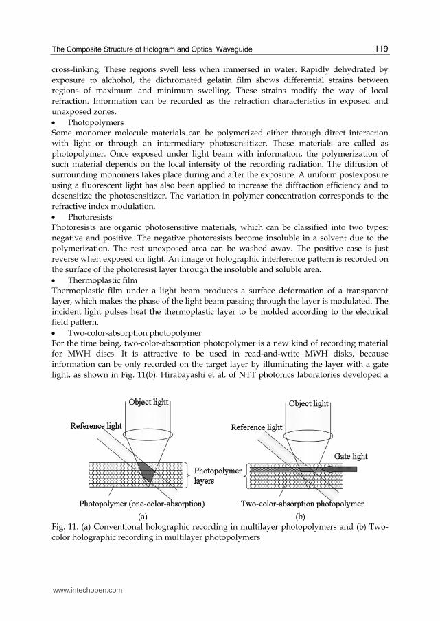
• Two-color-absorption photopolymer For the time being, two-color-absorption photopolymer is a new kind of recording material
for MWH discs. It is attractive to be used in read-and-write MWH disks, because
information can be only recorded on the target layer by illuminating the layer with a gate
light, as shown in Fig. 11(b). Hirabayashi et al. of NTT photonics laboratories developed a
(a) (b) Fig. 11. (a) Conventional holographic recording in multilayer photopolymers and (b) Two-
color holographic recording in multilayer photopolymers
www.intechopen.com
Holography, Research and Technologies
120
sensitive two-color-absorption photopolymer materials doped with is(silyl)pentathiophene
as a two-color-photosensitive dye and 2,2-dimethoxy-2-phenylacetophenone as a radical
photopolymerization initiator and working with a 660 nm interference light and a 410 nm
gate light. In 2004, Fujitsuka et al. reported that oligothiophenes show two-color absorption,
and Shimizu et al. recently found that the stepwise two-color absorption of the
oligothiophene in a Zeonex (Zeon Co.) matrix followed by energy transfer to an aryl azide in
the matrix is efficient for two-color recording and may be applicable to holographic
recording in multilayer thin films.
3. Optical interconnections based on optical waveguides holography
3.1 Introduction to optical interconnection
The term “optical interconnection” is often called simply “optical wiring” or “optical
interconnect” and can be interpreted in the broadest sense of the word as “any
interconnection using optical means”. In term of linkages using optical means, optical fiber
communication has been in practical use for more than twenty years, mainly for long
distance links. In contrast, there has not been a strong need for short-reach optical links.
However, as the problems of associated with hard-wired links become more apparent, this
approach is gathering new focus. Optical interconnection is the most promising candidate
for hard-wired circuitry. As optics become a major networking media in all communications
needs, optical interconnects will also play an important role in interconnecting processors in
parallel and distributed computing systems. Optical interconnect not only can provide
much more connections than a traditional electronic interconnect, but also can offer much
richer communication patterns for various networking applications. Such an optical
interconnect can be used to serve as a cross-connect in a wide-area communication network
or to provide high-speed interconnections among a group of processors in a parallel and
distributed computing system.
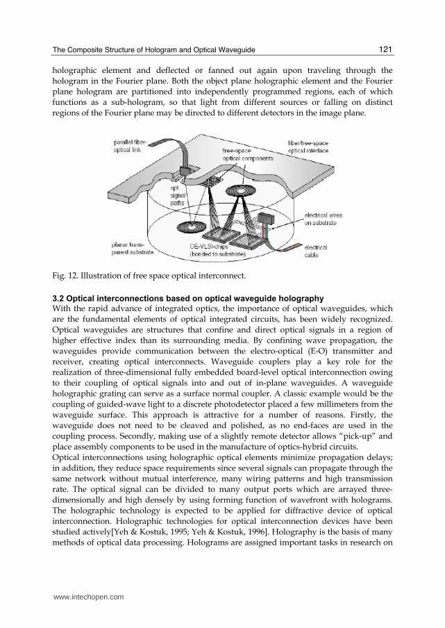
Optical interconnections may be formed in substrates with waveguide structures and
through the use of optical fiber, or in free-space either by beam spreading, or using
holograms. The former is referred to as index-guided optical interconnection and the latter
is referred as free-space optical interconnection. Fig. 12 depicts an example of free space
interconnects [Gruber, et al., 2000]. A space between two circuit boards or a circuit board
and optical interface board is purely empty. Light signals coming out from the sources
propagate to designated location on the other substrate.
The purpose of the optical interconnection is to replace the electrical wire with the optical
waveguide and associated optical devices. The smaller area the optical waveguide occupies on the chip area, the better integration the chip may have. All these approaches may be used to form reconfigurable interconnects with active components such as couplers for waveguides and optical fibers, modulators for beam spreading, and photo-refractive
materials as dynamic holograms. Fixed interconnects are adequate for many purposes and don't require the use of active beam-steering components. Free-space optical interconnections work in a three-dimensional volume in order to
transport the signals to the desired locations. An earlier model of free-space interconnection
is similar to a Fourier-plane imaging system with beam-deviating elements. The system has
an array of sources in the object plane and an array of detectors in the image plane.
Generally speaking, the light leaving the sources is deflected or fanned out upon passing a
www.intechopen.com
The Composite Structure of Hologram and Optical Waveguide
121
holographic element and deflected or fanned out again upon traveling through the
hologram in the Fourier plane. Both the object plane holographic element and the Fourier
plane hologram are partitioned into independently programmed regions, each of which
functions as a sub-hologram, so that light from different sources or falling on distinct
regions of the Fourier plane may be directed to different detectors in the image plane.
Fig. 12. Illustration of free space optical interconnect.
3.2 Optical interconnections based on optical waveguide holography
With the rapid advance of integrated optics, the importance of optical waveguides, which
are the fundamental elements of optical integrated circuits, has been widely recognized.
Optical waveguides are structures that confine and direct optical signals in a region of
higher effective index than its surrounding media. By confining wave propagation, the
waveguides provide communication between the electro-optical (E-O) transmitter and
receiver, creating optical interconnects. Waveguide couplers play a key role for the
realization of three-dimensional fully embedded board-level optical interconnection owing
to their coupling of optical signals into and out of in-plane waveguides. A waveguide
holographic grating can serve as a surface normal coupler. A classic example would be the
coupling of guided-wave light to a discrete photodetector placed a few millimeters from the
waveguide surface. This approach is attractive for a number of reasons. Firstly, the
waveguide does not need to be cleaved and polished, as no end-faces are used in the
coupling process. Secondly, making use of a slightly remote detector allows “pick-up” and
place assembly components to be used in the manufacture of optics-hybrid circuits.
Optical interconnections using holographic optical elements minimize propagation delays;
in addition, they reduce space requirements since several signals can propagate through the
same network without mutual interference, many wiring patterns and high transmission
rate. The optical signal can be divided to many output ports which are arrayed three-
dimensionally and high densely by using forming function of wavefront with holograms.
The holographic technology is expected to be applied for diffractive device of optical
interconnection. Holographic technologies for optical interconnection devices have been
studied actively[Yeh & Kostuk, 1995; Yeh & Kostuk, 1996]. Holography is the basis of many
methods of optical data processing. Holograms are assigned important tasks in research on
www.intechopen.com
Holography, Research and Technologies
122
optical interconnections. Particular interest attaches to multifocus lenses for matrix
processors and optical synchronization systems, and also to focusing devices that carry out
prescribed transformations of wave fronts. By using various types of holograms,
interconnections can be either fixed or variable. Dynamic holograms can make these
interconnections dynamic; in addition, the method of wave-front reversal is the best
physical basis for the development of associative two-dimensional memory. Holograms are
also indispensable in one- and two- dimensional analog-digital converters [Honma et al.,
2007].
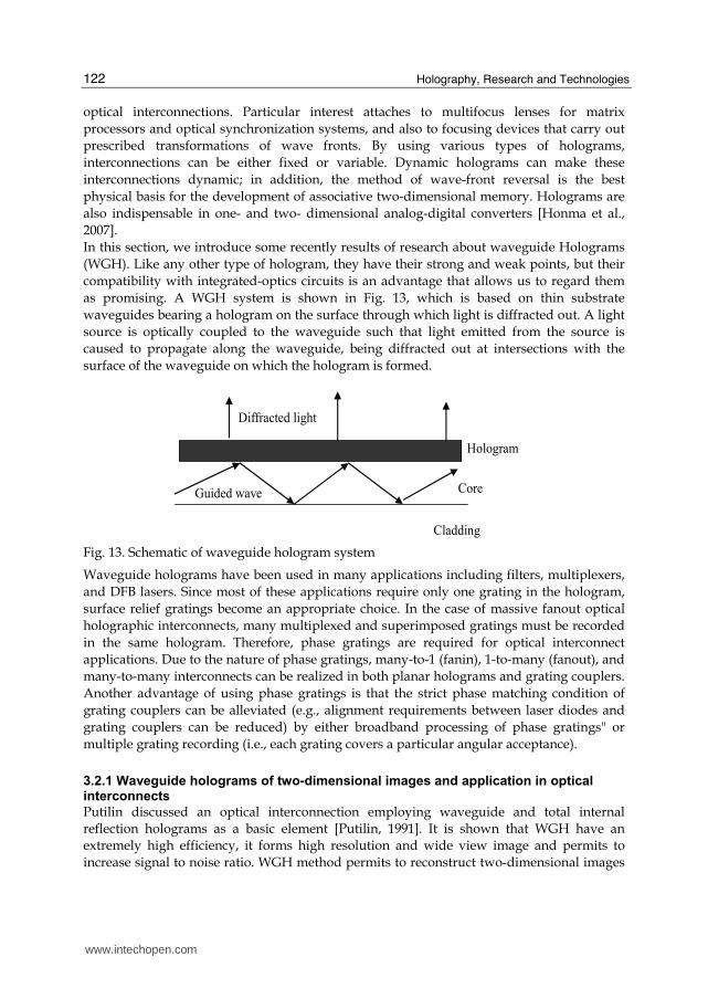
In this section, we introduce some recently results of research about waveguide Holograms
(WGH). Like any other type of hologram, they have their strong and weak points, but their
compatibility with integrated-optics circuits is an advantage that allows us to regard them
as promising. A WGH system is shown in Fig. 13, which is based on thin substrate
waveguides bearing a hologram on the surface through which light is diffracted out. A light
source is optically coupled to the waveguide such that light emitted from the source is
caused to propagate along the waveguide, being diffracted out at intersections with the
surface of the waveguide on which the hologram is formed.
Diffracted light
Guided wave
Hologram
Core
Cladding
Fig. 13. Schematic of waveguide hologram system
Waveguide holograms have been used in many applications including filters, multiplexers,
and DFB lasers. Since most of these applications require only one grating in the hologram,
surface relief gratings become an appropriate choice. In the case of massive fanout optical
holographic interconnects, many multiplexed and superimposed gratings must be recorded
in the same hologram. Therefore, phase gratings are required for optical interconnect
applications. Due to the nature of phase gratings, many-to-1 (fanin), 1-to-many (fanout), and
many-to-many interconnects can be realized in both planar holograms and grating couplers.
Another advantage of using phase gratings is that the strict phase matching condition of
grating couplers can be alleviated (e.g., alignment requirements between laser diodes and
grating couplers can be reduced) by either broadband processing of phase gratings" or
multiple grating recording (i.e., each grating covers a particular angular acceptance).
3.2.1 Waveguide holograms of two-dimensional images and application in optical interconnects
Putilin discussed an optical interconnection employing waveguide and total internal reflection holograms as a basic element [Putilin, 1991]. It is shown that WGH have an extremely high efficiency, it forms high resolution and wide view image and permits to
increase signal to noise ratio. WGH method permits to reconstruct two-dimensional images
www.intechopen.com
The Composite Structure of Hologram and Optical Waveguide
123
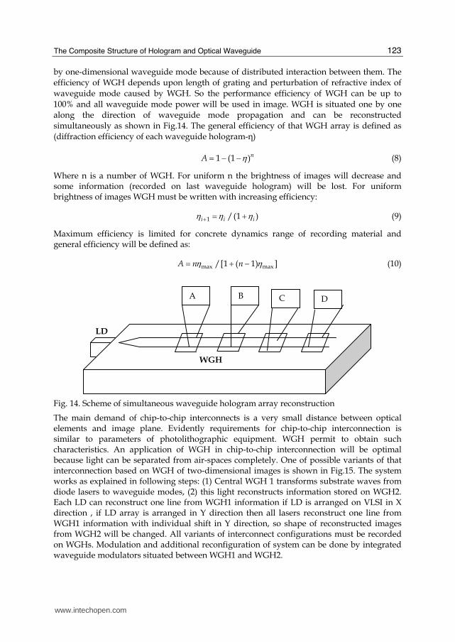
by one-dimensional waveguide mode because of distributed interaction between them. The efficiency of WGH depends upon length of grating and perturbation of refractive index of waveguide mode caused by WGH. So the performance efficiency of WGH can be up to
100% and all waveguide mode power will be used in image. WGH is situated one by one along the direction of waveguide mode propagation and can be reconstructed simultaneously as shown in Fig.14. The general efficiency of that WGH array is defined as (diffraction efficiency of each waveguide hologram-η)
1 (1 )nA η= − − (8)
Where n is a number of WGH. For uniform n the brightness of images will decrease and some information (recorded on last waveguide hologram) will be lost. For uniform brightness of images WGH must be written with increasing efficiency:
1 /(1 )i i iη η η+ = + (9)
Maximum efficiency is limited for concrete dynamics range of recording material and general efficiency will be defined as:
max max/[1 ( 1) ]A n nη η= + − (10)
Fig. 14. Scheme of simultaneous waveguide hologram array reconstruction
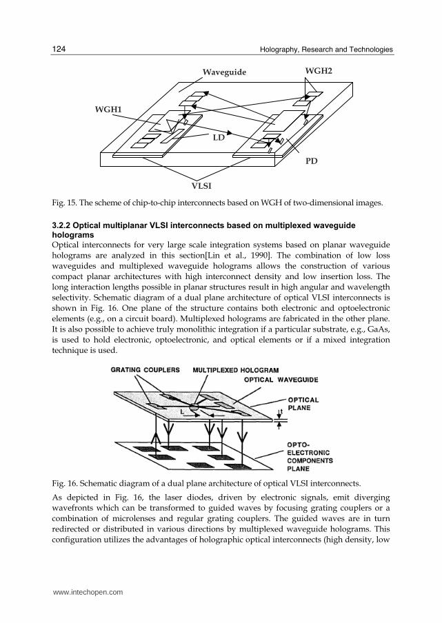
The main demand of chip-to-chip interconnects is a very small distance between optical elements and image plane. Evidently requirements for chip-to-chip interconnection is similar to parameters of photolithographic equipment. WGH permit to obtain such characteristics. An application of WGH in chip-to-chip interconnection will be optimal because light can be separated from air-spaces completely. One of possible variants of that interconnection based on WGH of two-dimensional images is shown in Fig.15. The system works as explained in following steps: (1) Central WGH 1 transforms substrate waves from diode lasers to waveguide modes, (2) this light reconstructs information stored on WGH2. Each LD can reconstruct one line from WGH1 information if LD is arranged on VLSI in X direction , if LD array is arranged in Y direction then all lasers reconstruct one line from WGH1 information with individual shift in Y direction, so shape of reconstructed images from WGH2 will be changed. All variants of interconnect configurations must be recorded on WGHs. Modulation and additional reconfiguration of system can be done by integrated waveguide modulators situated between WGH1 and WGH2.
A B C D
LD
WGH
www.intechopen.com
Holography, Research and Technologies
124
Waveguide
VLSI
WGH2
WGH1
LD
PD
Fig. 15. The scheme of chip-to-chip interconnects based on WGH of two-dimensional images.
3.2.2 Optical multiplanar VLSI interconnects based on multiplexed waveguide holograms
Optical interconnects for very large scale integration systems based on planar waveguide
holograms are analyzed in this section[Lin et al., 1990]. The combination of low loss
waveguides and multiplexed waveguide holograms allows the construction of various
compact planar architectures with high interconnect density and low insertion loss. The
long interaction lengths possible in planar structures result in high angular and wavelength
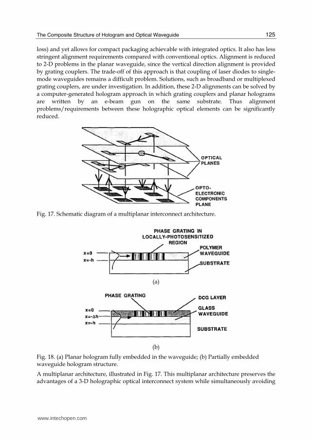
selectivity. Schematic diagram of a dual plane architecture of optical VLSI interconnects is
shown in Fig. 16. One plane of the structure contains both electronic and optoelectronic
elements (e.g., on a circuit board). Multiplexed holograms are fabricated in the other plane.
It is also possible to achieve truly monolithic integration if a particular substrate, e.g., GaAs,
is used to hold electronic, optoelectronic, and optical elements or if a mixed integration
technique is used.
Fig. 16. Schematic diagram of a dual plane architecture of optical VLSI interconnects.
As depicted in Fig. 16, the laser diodes, driven by electronic signals, emit diverging
wavefronts which can be transformed to guided waves by focusing grating couplers or a
combination of microlenses and regular grating couplers. The guided waves are in turn
redirected or distributed in various directions by multiplexed waveguide holograms. This
configuration utilizes the advantages of holographic optical interconnects (high density, low
www.intechopen.com
The Composite Structure of Hologram and Optical Waveguide
125
loss) and yet allows for compact packaging achievable with integrated optics. It also has less
stringent alignment requirements compared with conventional optics. Alignment is reduced
to 2-D problems in the planar waveguide, since the vertical direction alignment is provided
by grating couplers. The trade-off of this approach is that coupling of laser diodes to single-
mode waveguides remains a difficult problem. Solutions, such as broadband or multiplexed
grating couplers, are under investigation. In addition, these 2-D alignments can be solved by
a computer-generated hologram approach in which grating couplers and planar holograms
are written by an e-beam gun on the same substrate. Thus alignment
problems/requirements between these holographic optical elements can be significantly
reduced.
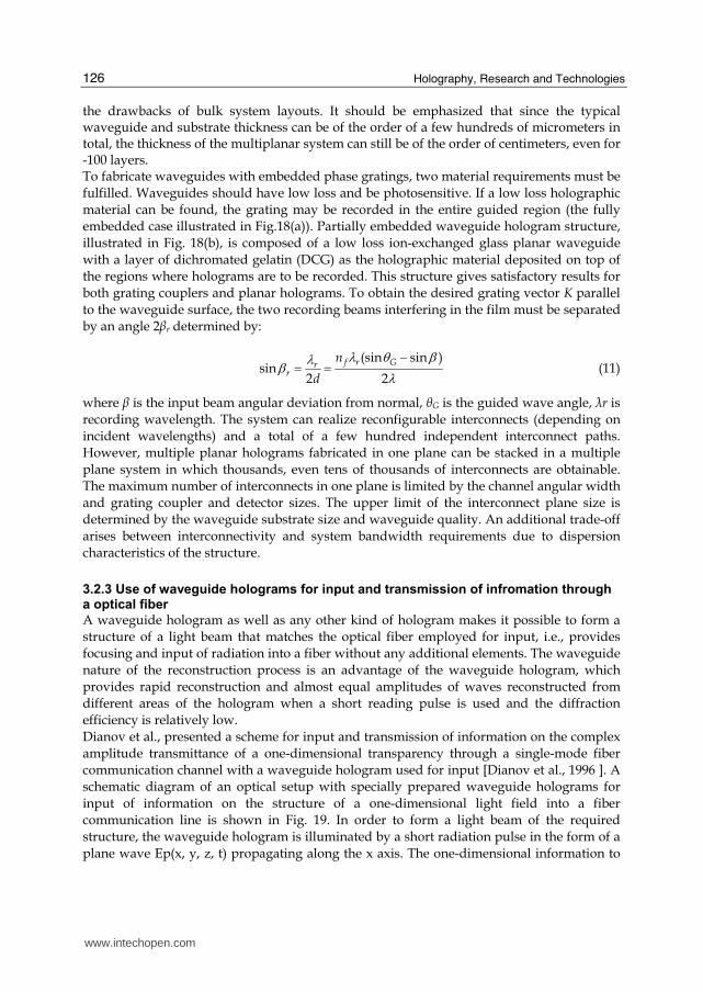
Fig. 17. Schematic diagram of a multiplanar interconnect architecture.
(a)
(b)
Fig. 18. (a) Planar hologram fully embedded in the waveguide; (b) Partially embedded waveguide hologram structure.
A multiplanar architecture, illustrated in Fig. 17. This multiplanar architecture preserves the advantages of a 3-D holographic optical interconnect system while simultaneously avoiding
www.intechopen.com
Holography, Research and Technologies
126
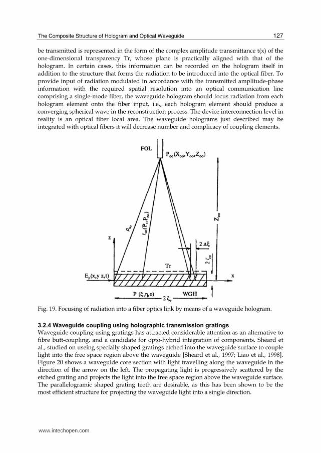
the drawbacks of bulk system layouts. It should be emphasized that since the typical waveguide and substrate thickness can be of the order of a few hundreds of micrometers in total, the thickness of the multiplanar system can still be of the order of centimeters, even for -100 layers. To fabricate waveguides with embedded phase gratings, two material requirements must be
fulfilled. Waveguides should have low loss and be photosensitive. If a low loss holographic material can be found, the grating may be recorded in the entire guided region (the fully embedded case illustrated in Fig.18(a)). Partially embedded waveguide hologram structure, illustrated in Fig. 18(b), is composed of a low loss ion-exchanged glass planar waveguide
with a layer of dichromated gelatin (DCG) as the holographic material deposited on top of the regions where holograms are to be recorded. This structure gives satisfactory results for both grating couplers and planar holograms. To obtain the desired grating vector K parallel
to the waveguide surface, the two recording beams interfering in the film must be separated by an angle 2βr determined by:
(sin sin )
sin2 2
f r Grr
n
d
λ θ βλβ λ−= = (11)
where β is the input beam angular deviation from normal, θG is the guided wave angle, λr is
recording wavelength. The system can realize reconfigurable interconnects (depending on incident wavelengths) and a total of a few hundred independent interconnect paths. However, multiple planar holograms fabricated in one plane can be stacked in a multiple
plane system in which thousands, even tens of thousands of interconnects are obtainable. The maximum number of interconnects in one plane is limited by the channel angular width and grating coupler and detector sizes. The upper limit of the interconnect plane size is determined by the waveguide substrate size and waveguide quality. An additional trade-off
arises between interconnectivity and system bandwidth requirements due to dispersion characteristics of the structure.
3.2.3 Use of waveguide holograms for input and transmission of infromation through a optical fiber
A waveguide hologram as well as any other kind of hologram makes it possible to form a structure of a light beam that matches the optical fiber employed for input, i.e., provides focusing and input of radiation into a fiber without any additional elements. The waveguide nature of the reconstruction process is an advantage of the waveguide hologram, which
provides rapid reconstruction and almost equal amplitudes of waves reconstructed from different areas of the hologram when a short reading pulse is used and the diffraction efficiency is relatively low.
Dianov et al., presented a scheme for input and transmission of information on the complex amplitude transmittance of a one-dimensional transparency through a single-mode fiber communication channel with a waveguide hologram used for input [Dianov et al., 1996 ]. A schematic diagram of an optical setup with specially prepared waveguide holograms for
input of information on the structure of a one-dimensional light field into a fiber communication line is shown in Fig. 19. In order to form a light beam of the required structure, the waveguide hologram is illuminated by a short radiation pulse in the form of a
plane wave Ep(x, y, z, t) propagating along the x axis. The one-dimensional information to
www.intechopen.com
The Composite Structure of Hologram and Optical Waveguide
127
be transmitted is represented in the form of the complex amplitude transmittance t(x) of the one-dimensional transparency Tr, whose plane is practically aligned with that of the hologram. In certain cases, this information can be recorded on the hologram itself in
addition to the structure that forms the radiation to be introduced into the optical fiber. To provide input of radiation modulated in accordance with the transmitted amplitude-phase information with the required spatial resolution into an optical communication line comprising a single-mode fiber, the waveguide hologram should focus radiation from each
hologram element onto the fiber input, i.e., each hologram element should produce a converging spherical wave in the reconstruction process. The device interconnection level in reality is an optical fiber local area. The waveguide holograms just described may be integrated with optical fibers it will decrease number and complicacy of coupling elements.
Fig. 19. Focusing of radiation into a fiber optics link by means of a waveguide hologram.
3.2.4 Waveguide coupling using holographic transmission gratings
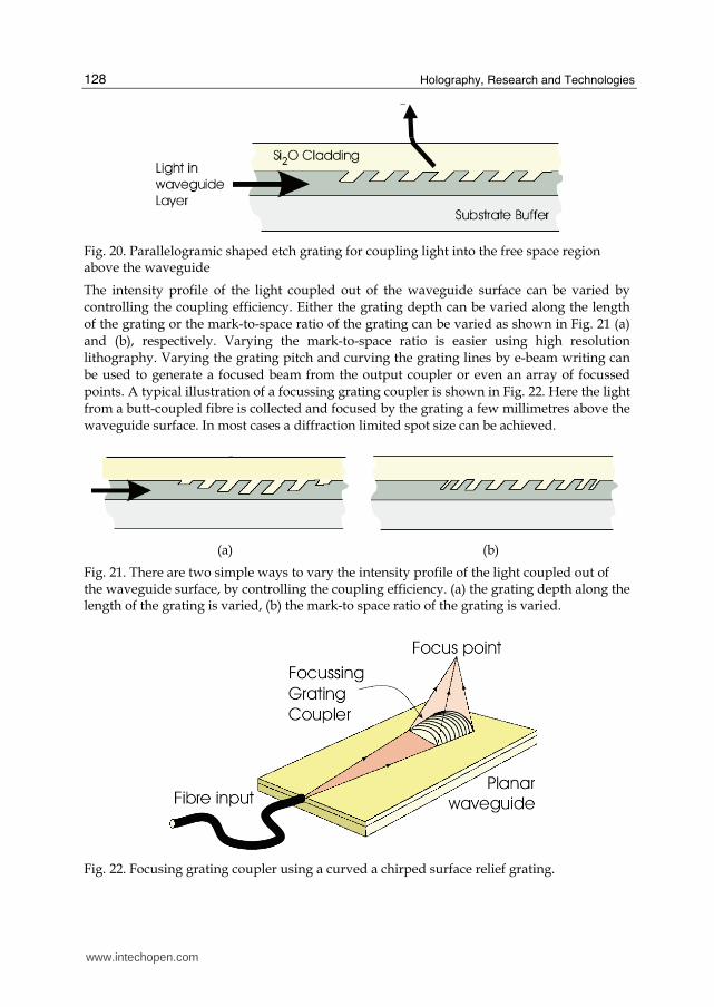
Waveguide coupling using gratings has attracted considerable attention as an alternative to fibre butt-coupling, and a candidate for opto-hybrid integration of components. Sheard et al., studied on useing specially shaped gratings etched into the waveguide surface to couple light into the free space region above the waveguide [Sheard et al., 1997; Liao et al., 1998]. Figure 20 shows a waveguide core section with light travelling along the waveguide in the direction of the arrow on the left. The propagating light is progressively scattered by the etched grating and projects the light into the free space region above the waveguide surface. The parallelogramic shaped grating teeth are desirable, as this has been shown to be the most efficient structure for projecting the waveguide light into a single direction.
www.intechopen.com
Holography, Research and Technologies
128
Fig. 20. Parallelogramic shaped etch grating for coupling light into the free space region above the waveguide
The intensity profile of the light coupled out of the waveguide surface can be varied by controlling the coupling efficiency. Either the grating depth can be varied along the length
of the grating or the mark-to-space ratio of the grating can be varied as shown in Fig. 21 (a) and (b), respectively. Varying the mark-to-space ratio is easier using high resolution lithography. Varying the grating pitch and curving the grating lines by e-beam writing can be used to generate a focused beam from the output coupler or even an array of focussed
points. A typical illustration of a focussing grating coupler is shown in Fig. 22. Here the light from a butt-coupled fibre is collected and focused by the grating a few millimetres above the waveguide surface. In most cases a diffraction limited spot size can be achieved.
(a) (b)
Fig. 21. There are two simple ways to vary the intensity profile of the light coupled out of the waveguide surface, by controlling the coupling efficiency. (a) the grating depth along the length of the grating is varied, (b) the mark-to space ratio of the grating is varied.
Fig. 22. Focusing grating coupler using a curved a chirped surface relief grating.
www.intechopen.com
The Composite Structure of Hologram and Optical Waveguide
129
Because of its periodic nature, the grating perturbs the waveguide modes in the region underneath the grating, thus causing each one of them to have a set of spatial harmonics with z-direction propagation constants given by
0
2v
νπβ β= + Λ (12)
where ┥=0, ± 1, ± 2, . . . , and where Λ is the periodicity of the grating. The fundamental factor β0 is approximately equal to the βm of the particular mode in the waveguide region not covered by the grating. The principal advantage of the grating coupler is that, once
fabricated, it is an integral part of the waveguide structure. Hence, its coupling efficiency remains constant and is not altered appreciably by vibration or ambient conditions.
4. The holographic waveguide for see-through planar display
The technology of see-through planar display (i.e. head-up display) is now used in the fields of military aviation, commercial aircraft, automobiles and other applications. A
conventional see-through planar display system contains three primary components: a combiner, a projector unit, and a video-generating computer, so the size of the entire instrument is quite large, as shown in Fig. 23. Because the holographic waveguide itself is transparent to the free-space light beams in the
direction of perpendicular to waveguide, the observer can view the image produced by the hologram and at the same time can see through the hologram to view the scene at the opposite side of the hologram. This property is very useful for head-up display technology
to eyewear display.
Fig. 23. A type of head-up display system.
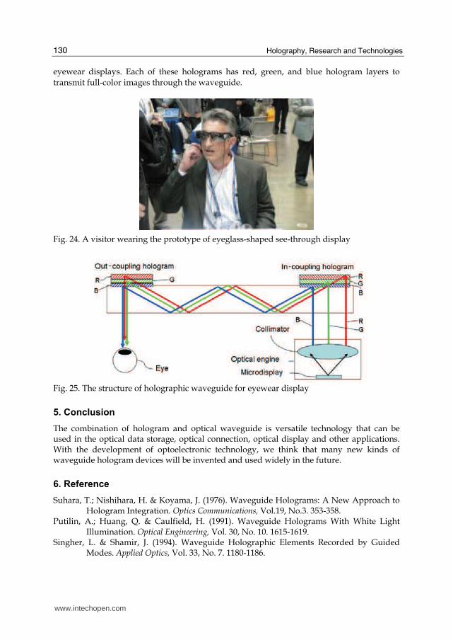
In 2008, Sony Co. reported an eyeglass-shaped see-through display that can show full color
video images, as shown in Fig. 24, and the holographic waveguide is the key component
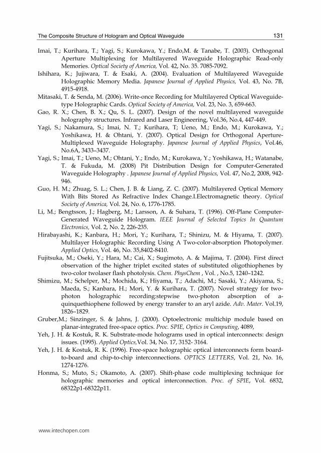
that realized the structure and display method in this sample. Fig. 25 illustrates this type
structure of the holographic planar waveguide of the eyewear display [Mukawa et al., 2009].
The waveguide has an in-coupling and an out-coupling reflection volume hologram which
have exactly the same fringe pattern and a mirror symmetrically positioned. Reflection
volume holograms were employed because their diffraction bandwidths are much smaller
than those of transmission holograms and could potentially enlarge the field of view of the
www.intechopen.com
Holography, Research and Technologies
130
eyewear displays. Each of these holograms has red, green, and blue hologram layers to
transmit full-color images through the waveguide.
Fig. 24. A visitor wearing the prototype of eyeglass-shaped see-through display
Fig. 25. The structure of holographic waveguide for eyewear display
5. Conclusion
The combination of hologram and optical waveguide is versatile technology that can be used in the optical data storage, optical connection, optical display and other applications. With the development of optoelectronic technology, we think that many new kinds of waveguide hologram devices will be invented and used widely in the future.
6. Reference
Suhara, T.; Nishihara, H. & Koyama, J. (1976). Waveguide Holograms: A New Approach to Hologram Integration. Optics Communications, Vol.19, No.3. 353-358.
Putilin, A.; Huang, Q. & Caulfield, H. (1991). Waveguide Holograms With White Light Illumination. Optical Engineering, Vol. 30, No. 10. 1615-1619.
Singher, L. & Shamir, J. (1994). Waveguide Holographic Elements Recorded by Guided Modes. Applied Optics, Vol. 33, No. 7. 1180-1186.
www.intechopen.com
The Composite Structure of Hologram and Optical Waveguide
131
Imai, T.; Kurihara, T.; Yagi, S.; Kurokawa, Y.; Endo,M. & Tanabe, T. (2003). Orthogonal
Aperture Multiplexing for Multilayered Waveguide Holographic Read-only
Memories. Optical Society of America, Vol. 42, No. 35. 7085-7092.
Ishihara, K.; Jujiwara, T. & Esaki, A. (2004). Evaluation of Multilayered Waveguide
Holographic Memory Media. Japanese Journal of Applied Physics, Vol. 43, No. 7B,
4915-4918.
Mitasaki, T. & Senda, M. (2006). Write-once Recording for Multilayered Optical Waveguide-
type Holographic Cards. Optical Society of America, Vol. 23, No. 3, 659-663.
Gao, R. X.; Chen, B. X.; Qu, S. L. (2007). Design of the novel multilayered waveguide
holography structures. Infrared and Laser Engineering, Vol.36, No.4, 447-449.
Yagi, S.; Nakamura, S.; Imai, N. T.; Kurihara, T; Ueno, M.; Endo, M.; Kurokawa, Y.;
Yoshikawa, H. & Ohtani, Y. (2007). Optical Design for Orthogonal Aperture-
Multiplexed Waveguide Holography. Japanese Journal of Applied Physics, Vol.46,
No.6A, 3433–3437.
Yagi, S.; Imai, T.; Ueno, M.; Ohtani, Y.; Endo, M.; Kurokawa, Y.; Yoshikawa, H.; Watanabe,
T. & Fukuda, M. (2008) Pit Distribution Design for Computer-Generated
Waveguide Holography . Japanese Journal of Applied Physics, Vol. 47, No.2, 2008, 942-
946.
Guo, H. M.; Zhuag, S. L.; Chen, J. B. & Liang, Z. C. (2007). Multilayered Optical Memory
With Bits Stored As Refractive Index Change.I.Electromagnetic theory. Optical
Society of America, Vol. 24, No. 6, 1776-1785.
Li, M.; Bengtsson, J.; Hagberg, M.; Larsson, A. & Suhara, T. (1996). Off-Plane Computer-
Generated Waveguide Hologram. IEEE Journal of Selected Topics In Quantum
Electronics, Vol. 2, No. 2, 226-235.
Hirabayashi, K.; Kanbara, H.; Mori, Y.; Kurihara, T.; Shinizu, M. & Hiyama, T. (2007).
Multilayer Holographic Recording Using A Two-color-absorption Photopolymer.
Applied Optics, Vol. 46, No. 35,8402-8410.
Fujitsuka, M.; Oseki, Y.; Hara, M.; Cai, X.; Sugimoto, A. & Majima, T. (2004). First direct
observation of the higher triplet excited states of substituted oligothiophenes by
two-color twolaser flash photolysis. Chem. PhysChem , Vol. , No.5, 1240–1242.
Shimizu, M.; Schelper, M.; Mochida, K.; Hiyama, T.; Adachi, M.; Sasaki, Y.; Akiyama, S.;
Maeda, S.; Kanbara, H.; Mori, Y. & Kurihara, T. (2007). Novel strategy for two-
photon holographic recording:stepwise two-photon absorption of a-
quinquethiophene followed by energy transfer to an aryl azide. Adv. Mater. Vol.19,
1826–1829.
Gruber,M.; Sinzinger, S. & Jahns, J. (2000). Optoelectronic multichip module based on
planar-integrated free-space optics. Proc. SPIE, Optics in Computing, 4089,
Yeh, J. H. & Kostuk, R. K. Substrate-mode holograms used in optical interconnects: design
issues. (1995). Applied Optics,Vol. 34, No. 17, 3152- 3164.
Yeh, J. H. & Kostuk, R. K. (1996). Free-space holographic optical interconnects form board-
to-board and chip-to-chip interconnections. OPTICS LETTERS, Vol. 21, No. 16,
1274-1276.
Honma, S.; Muto, S.; Okamoto, A. (2007). Shift-phase code multiplexing technique for
holographic memories and optical interconnection. Proc. of SPIE, Vol. 6832,
68322p1-68322p11.
www.intechopen.com
Holography, Research and Technologies
132
Putilin, A. N. (1991). Optical interconnections based on waveguide holograms. Proc. of SPIE,
Vol. 1621, 93-101.
Lin, F; Eva M.; Strzelecki, E. M. & Jannson, T. (1990). Optical multiplanar VLSI interconnects
based on multiplexed waveguide holograms. Applied Optics,Vol. 29, No. 8, 1126-
1133.
Dianov, E. M.; Putilin, A. N. & Zubov, V. A. (1996). Use of waveguide holograms for input
and transmission of information on a light field through a single-mode optical
fiber. Journal of Russian Laser Research, Vol. 17, No. 1, 55-84.
Sheard S. J.; Liao T. D.; Yang G. G.; Prewett P. D. & Zhu J. G. (1997). Focusing waveguide
grating coupler using diffractive doublet. Applied Optics, Vol. 36, No. 19, 4349-4353.
Liao T. D. & Sheard S. J. (1998). Radiation characteristics of waveguide diffractive doublets.
Applied Optics, Vol.37, No.10, 1776-1783.
Mukawa, H; Akutsu, K.; Matsumura, I.; Nakano, S.; Yoshida, T.; Kuwahara, M. & Aiki, K.
(2009). A full-color eyewear display using planar waveguides with reflection
volume holograms. Journal of the society for information display, Vol. 17, No. 3, 185-
193
www.intechopen.com
Holography, Research and TechnologiesEdited by Prof. Joseph Rosen
ISBN 978-953-307-227-2Hard cover, 454 pagesPublisher InTechPublished online 28, February, 2011Published in print edition February, 2011
InTech EuropeUniversity Campus STeP Ri Slavka Krautzeka 83/A 51000 Rijeka, Croatia Phone: +385 (51) 770 447 Fax: +385 (51) 686 166www.intechopen.com
InTech ChinaUnit 405, Office Block, Hotel Equatorial Shanghai No.65, Yan An Road (West), Shanghai, 200040, China
Phone: +86-21-62489820 Fax: +86-21-62489821
Holography has recently become a field of much interest because of the many new applications implementedby various holographic techniques. This book is a collection of 22 excellent chapters written by various experts,and it covers various aspects of holography. The chapters of the book are organized in six sections, startingwith theory, continuing with materials, techniques, applications as well as digital algorithms, and finally endingwith non-optical holograms. The book contains recent outputs from researches belonging to different researchgroups worldwide, providing a rich diversity of approaches to the topic of holography.
How to referenceIn order to correctly reference this scholarly work, feel free to copy and paste the following:
Renxi Gao and Wenjun Liu (2011). The Composite Structure of Hologram and Optical Waveguide,Holography, Research and Technologies, Prof. Joseph Rosen (Ed.), ISBN: 978-953-307-227-2, InTech,Available from: http://www.intechopen.com/books/holography-research-and-technologies/the-composite-structure-of-hologram-and-optical-waveguide

© 2011 The Author(s). Licensee IntechOpen. This chapter is distributedunder the terms of the Creative Commons Attribution-NonCommercial-ShareAlike-3.0 License, which permits use, distribution and reproduction fornon-commercial purposes, provided the original is properly cited andderivative works building on this content are distributed under the samelicense.


![[Challenge:Future] Hologram Portable Media Gadget](https://img.pdfslide.us/doc/110x75/549c04acb4795991318b4635/challengefuture-hologram-portable-media-gadget.jpg)