Embed Size (px)
Citation preview
The “Calculative” Calculator Interactive Digital Calculator
Chandler Connolly, Sarah Elhage, Matthew Shina, Daniyah Alaswad Electrical and Computer Engineering Department
School of Engineering and Computer Science Oakland University, Rochester, MI
E-mails: [email protected], [email protected], [email protected], [email protected]
ABSTRACT The final project was to build an interactive digital
calculator capable of performing addition, subtraction, multiplication, and division. The primary motivation was that a calculator is an interesting way to incorporate all of the VHDL techniques previously learned in the lab. Things that became apparent during the design process were the difficulty with implementing an external keyboard, and designing a clever input method. Overall takeaways are that the project works, although can be pretty buggy in certain instances. Further troubleshooting would be necessary for a more extensive and thorough keyboard interface.
I. INTRODUCTION
The scope of this project was to design a fully functioning calculator consisting of the addition, subtraction, multiplication, and division operators. This project proved to be a great challenge considering it required the implementation of all of the previous labs such as the full adder, multiplier, divider, and memory register. Not only did it call for integration of all four operations, but also an external keyboard for input purposes. The design made use of many of the components covered in class including counters, multiplexers, shift registers, full adders, and state machines. However, some components not covered in class that had to be researched further were the latch and clock divider. A very appealing aspect of designing a calculator is that it has many applications. They are used every day in society and specifically in almost every computational device. It is one of the most powerful and widely used tools.
II. METHODOLOGY
A. Board Input & Keyboard Input
One of the areas that were more thoroughly designed was the input method. It was decided that aside from the keyboard, a board input method should also be implemented. The 5 buttons on the NEXYS board were used for digit input, function select, and calculate. The
leftmost switch was set as an enable for the keyboard once it’s been plugged in. Finally, the CPU Reset button was used to clear all the data and return zeros across the 7-segment display.
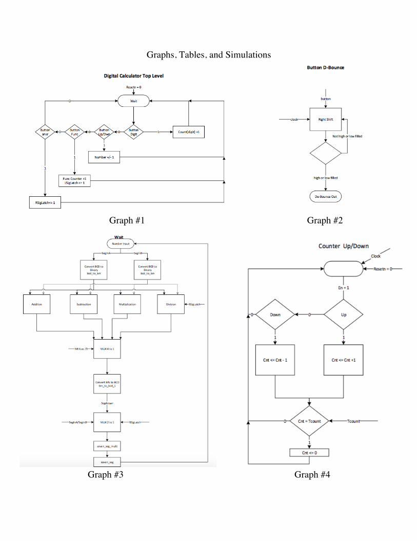
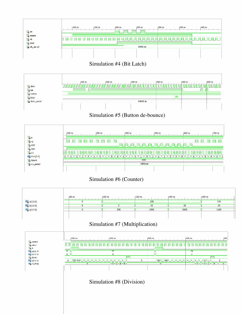
The code for the keyboard was taken from the class website, but modified a bit due to ongoing communication problems. The push buttons utilized the de-bounce mechanism shown in Graph 2 to determine if the button was pressed or not. We used a 32 bit shift register to collect 1s or 0s depending on how long the switch was pressed. In order for the value to change to either high or low, all 32 bits must be either high or low. Furthermore, if the value is initially high, it cannot go high once again until it is filled with 0s beforehand.
A system of counters was used to allow for the increasing and decreasing of individual digits on the NEXYS board. Referencing Graph 4 below, if the enable is high and the press of the “Up” button is detected, the count is programmed to increase by 1. If the enable is high and the “down” button is detected, the count will decrease by 1. The value would then increase or decrease until the count is equal to “Tcount”. That is essentially the thought process behind the clever entering of numbers and commands on the board.
B. Function & Display
The main schematics and ideas used for each individual function came from the previous labs. Each program was slightly modified to allow for 3 bit inputs and to work the overall top level design. Some aspects that required extra research to implement were the 7-segment display using a certain clock frequency to allow for all the digits to show simultaneously, and the latch mechanism.
Looking at the overall top level design whose schematic is shown in Graph 1, there were many different components used in order to get a thorough design. The “wait” at the top is constantly checking for button inputs. The “button digit” increments a counter from 0-3, which will control which single active 7-segment is being used. Then data is pulled from another counter incrementing from 0-9 based on the desired value. Once the function button is pressed, another counter from 0-3 will increment based on the desired
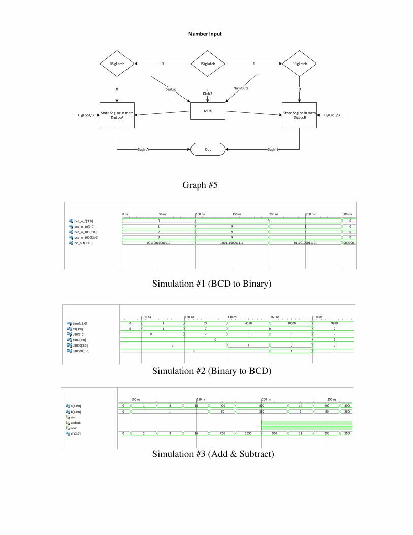
function. This also causes the “LSigLatch” to return a value of 1. When “LSigLatch” is high, it allows the rightmost 7-segment display to be editable so the user can now input those digits as well. Finally, when the calculate button is pressed, the RSigLatch will go high and cause the 7-segment display to change to the answer. Pressing the calculate button also enables the division function because at this point, both values have been entered and the quotient/remainder are calculable.
From a more specific standpoint, a binary to BCD converter is used to translate the inputs before they are entered into the respective operations. A 4X1 multiplexer then decides which function to send based on which function is selected on the board at the time. After a few more number conversions, the final answer is sent to display on the 7-segments panel. This is shown in Graph 3.
III. EXPERIMENTAL SETUP
The overall setup and testing that was done to validate the components of the project consisted mainly of using the ISE software as was done in the lab. Each component was designed separately and simulated separately. Once the timing and behavioral simulations acted as expected, that particular piece of code would be implemented into the overall structure. Due to the extremely large and complex files that were required to program this calculator, the testing was done incrementally and separately as the code progressed. This allowed for a much more organized and overall effective way to troubleshoot and work out bugs. The testing of the keyboard and button switches proved to be very difficult utilizing the timing simulations in the ISE program. They may not have been as precise as was initially desired, but both the keyboard and buttons still functioned relatively well. Other additional tools than the software itself, was the NEXYS board. In some cases, certain LEDs on the board were programmed to illuminate to verify the operation of certain signals. This was very useful in providing a visual aid when implementing the overall design on the board itself. No additional oscilloscope or multimeter and such were used since there was no primary use for them.
The expected results were that the keyboard and button switches could both be capable of inputting different digits into the 7-segment display. Another expectation was that all four operations functioned as normal. As a whole, the expected results matched up completely with the end results of the project.
IV. RESULTS
The end results of the project proved to be very close to what was initially expected. All of the implemented functions worked correctly and very well with the multiple input methods that were introduced. Some areas where the
results did not meet our expectations were with the keyboard. We had wanted the keyboard to work more seamlessly with the 7-segment display. An example is that although the keyboard was used to input the numbers, the digits would not auto-index over. Meaning, every slot in the 7-segment had to first be selected before the user typed the digit instead of being able to type the whole number (500 for example). The keyboard was extremely hard to simulate and troubleshoot. There was a lot of communications issues with the keyboard initially that were causing it to send incorrect and excess numbers over. However, this was slightly overcome by manipulating the code provided by Dr. Llamocca on the class website.
Along with the keyboard misbehaving, the push button switches on the NEXYS board weren’t operating quite as precisely as what was expected. Sometimes when pressed, the number would increment twice instead of once. The button de-bounce had a lot fine tuning done to it in order to correct this, however, we were still unable to get it exactly where we wanted it.
Another quite large issue that wasn’t fixed until late was the division function. All of the operations were taken from the labs done in the class; however, the division function was not working properly. It was later realized that the enable became “1” or high before the two numbers “A” and “B” were loaded. The enable had to be toggled but only once the two numbers were input.
Overall, we were very proud of the results of the project. It functioned just as expected, if not a little better in some areas regardless of certain setbacks. Many of the topics that our project consisted of correlated with those taught in class. The full adder, multiplier, divider, multiplexer, and register are some examples. The only area that yielded some unexplainable results was the external keyboard. Although its basic functionality was implemented, the various communications and simulation issues remain somewhat unclear to us. Various simulations of components are listed below in the “Graphs, Tables, and Simulations” portion of this report.
V. CONCLUSION In the end, this project was a great learning
experience because it incorporated all of the different things taught in the class. Not only did it incorporate each individual component such as state machines, adders, and registers, but also it required us to combine and implement every single one of them into one large encompassing design. There were also some areas that weren’t covered in the class that we had done additional research on such as latches and using pulse width modulation. For example, PWM was included as a last minute thought to lower the brightness of the LED so it would be easier to present in class. We used the 8 rightmost switches on the board to act as the 8 bit input for brightness control.
An aspect that had yet to be solved was the implementation of signed numbers. It was initially decided to include negative numbers, however, proved to be too difficult with the amount of time we had to design and troubleshoot the rest of the code. Some potential improvements that we would’ve liked to make are display and input capabilities. The keyboard and push buttons that were used to input each number weren’t as fluid as we had liked. The 7-segment display also doesn’t provide a lot of flexibility, resulting in many limited character combinations. If possible, a VGA display would have been very useful to have so that the numbers, functions, and answers could be displayed simultaneously. Regardless of all the issues, bugs, and potential improvements, the project was a huge success and a real great way to wrap up everything covered in the course.
VI. REFERENCES
[1] Larson, Scott. "PWM Generator (VHDL) - Logic - Eewiki." PWM Generator (VHDL) - Logic - Eewiki. N/A, n.d. Web. 27 Nov. 2016.
[2] N/A. "VHDL Code for BCD to Binary Conversion." VHDL Code for BCD to Binary Conversion. N/A, 7 Apr. 2015. Web. 28 Nov. 2016.
[3] Llamocca, Daniel. “Reconfigurable computing research laboratory.” Reconfigurable Computing Research Laboratory. 29 Apr. 2014. Web. 25 Nov. 2016.
[4] N/A. “8 bit binary to BCD converter - double dabble algorithm.” VHDL Guru. 21 May 2010. N/A. 22 Nov. 2016.
Graphs, Tables, and Simulations
Graph #1 Graph #2
Graph #3 Graph #4
Graph #5
Simulation #1 (BCD to Binary)
Simulation #2 (Binary to BCD)
Simulation #3 (Add & Subtract)
a[13:0] 0 1 2 15 400 800 14 400 800
b[13:0] 0 1 50 250 3 50 250
cin
addsub
cout
s[13:0] 0 2 3 16 450 1050 550 11 350 550
100 ns 150 ns 200 ns 250 ns
Number Input
LSigLatch
Store SegLoc in memDigLocA
0
DigLocA/3
RSigLatch 0 RSigLatch1
Store SegLoc in memDigLocB
0
DigLocB/3
SegInA Out SegInB
NumOuta
MUX
SegLocKbd/2
bcd_in_0[3:0] 0 9 0
bcd_in_10[3:0] 1 9 2 0
bcd_in_100[3:0] 2 9 4 0
bcd_in_1000[3:0] 3 9 6 0
bin_out[13:0] 00110010001010 10011100001111 01100100011101 000000…
0 ns 50 ns 100 ns 150 ns 200 ns 250 ns 300 ns
binin[15:0] 0 1 27 4050 10000 9999
d1[3:0] 0 1 7 0 9
d10[3:0] 0 2 5 0 9
d100[3:0] 0 9
d1000[3:0] 0 4 0 9
d10000[3:0] 0 1 0
100 ns 120 ns 140 ns 160 ns 180 ns
Simulation #4 (Bit Latch)
Simulation #5 (Button de-bounce)
Simulation #6 (Counter)
Simulation #7 (Multiplication)
Simulation #8 (Division)
100 ns 150 ns 200 ns 250 ns 300 ns 350 ns 400 ns
100 ns 200 ns 300 ns 400 ns 500 ns 600 ns
200 ns 300 ns 400 ns 500 ns 600 ns 700 ns
a[13:0] 0 100 116
b[13:0] 0 3 10 26 10
p[17:0] 0 300 1000 2600 1160
80 ns 100 ns 120 ns 140 ns 160 ns 180 ns
200 ns 300 ns 400 ns 500 ns 600 ns


![Watson Gets Personal - RealTechSupportCT/papers/selected_papers/Bohlen… · calculative and noncalculative actions [Callon&Law2003/5]. Thrift expanded the concept of disappearing](https://img.pdfslide.us/doc/110x75/5f52f3371e209d7cf4499ee7/watson-gets-personal-ctpapersselectedpapersbohlen-calculative-and-noncalculative.jpg)