Embed Size (px)
Citation preview
The analysis of TLM with high frequency coupling in PCB
design ZHAO Lian-qing1 ,LV Zheng-quan2
School of Electric and Electronic engineering , North China Electric Power University, Beijing 102206
1. [email protected] ,[email protected]
Abstract: With the help of the basic theory of transmission lines, two lines’ high-frequency interference coupling of the mathematical model is used to calculate the quantitative analysis of the transmission lines of high-frequency interference. At the same time, the common parameters of the parallel wires on PCB are set for the simulation and authentication under the Matlab and Ansoft tools respectively. This method for quantitative analysis of high-frequency coupling provides a reliable mathematical model. In the PCB circuit board designing, this model can be referred to reduce the coupling of high frequency interference.
Key words: EMC(electromagnetic compatibility);TLM(transmission lines model);PCB(printed circuit board)
1 Introduction With the development of new technologies, the rate of1
PCB alignment increasing, PCB circuit transmission line
effects become normal constraints of work. PCB has
become the transmission line alignment. Transmission
line is a fit in two or more effective end-to-end
transmission of power or signal transmission system. In a
multi- transmission lines of PCB system, the coupling
between transmission lines (including perceptual coupling
and capacitive coupling), would have two harmful effects:
First, it changes the bus crosstalk by the crosstalk
characteristics of the transmission line. Second, the
cross-talk produces the noise to the other transmission
line. In this case, a mathematical model to analyze the
parallel transmission lines in high-frequency crosstalk
cases is presented, including two parallel transmission
lines to simplify the circuit model. The analysis of the
relationship of two parallel lines' distance, the length of
two parallel lines, the distance from the source and the
transmission signal frequency with the voltage gain are
made based on this mathematical model. In order to solve
the problem of high-frequency cross-talk problem, a
reliable mathematical model and solution are
presented .Specifically we will introduce the model built
following.
2 Model Foundation Item:Project supported by the international
science and technology cooperation program(Grant Nos:2007DFA71250)
Figure 1 shows the two-transmission line under normal
circumstances. One of which we call a drive signal
transmission line, another line is the interference line.
when we load a drive signal on the drive signal line,
because of the high-frequency parasitic capacitance and
parasitic inductance’s effects , perturbed line will have a
sensor voltage and induced current, which in the specific
design of the PCB should be minimized strongly [1].
01Z
2lZ1lZ
02Z
sU
x
0
l
Figure 1 Two-wire transmission line model in PCB design
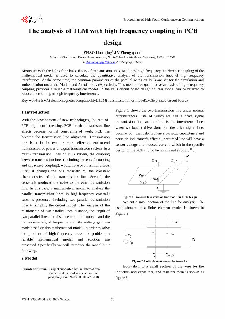
We cut a small section of the line for analysis. The
establishment of a finite element model is shown in
Figure 2;
i dii
u duu
lZgR
gU
x dxx
Figure 2 Finite element model for two-wire
Equivalent to a small section of the wire for the
inductors and capacitors, and resistors form is shown as
figure 3:
70
Proceedings of 14th Youth Conference on Communication
978-1-935068-01-3 © 2009 SciRes.
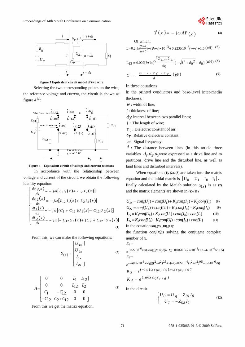
xLxR dii i
u duu
xG
xCgR
gU
x dxx
lZ
Figure 3 Equivalent circuit model of two wire
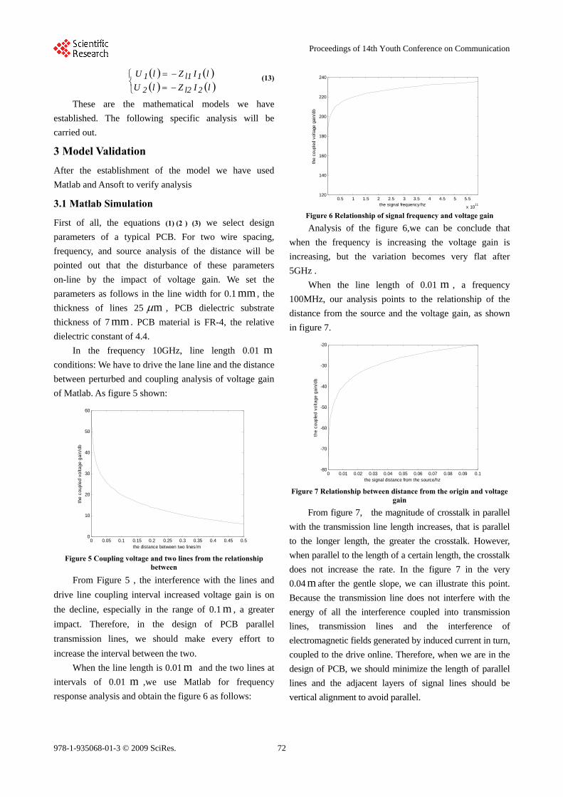
Selecting the two corresponding points on the wire,
the reference voltage and current, the circuit is shown as
figure 4 [2]:
)0(1
I )(1 xI
)(1 lI
)(1 xU
)(2 xI
)(1 lU
)(2 lI
)0(2
I
)(2 xU
)0(2
U
)0(1
U
)(2 lU
01Z
gU
02Z
1lZ
2lZ
xl0
Figure 4 Equivalent circuit of voltage and current relations
In accordance with the relationship between
voltage and current of the circuit, we obtain the following
identity equation:
xUCCxUCjdx
xdI
xUCxUCCjdx
xdI
xILxILjdx
xdu
xILxILjdx
xdu
21221122
21211211
221122
212111
)(
)(
(1)
From this, we can make the following equations:
2x
1x
2x
1x
xY
I
I
U
U
(2)
(3)
00
00
00
00
12212
121
212
121
CCC
CC
LL
LL
A
From this we get the matrix equation:
xAYxY j (4)
Of which:
1.5])(3100.2235310)(2)2
0.2[ln(L
twthtw
th Η)( (5)
]02
02)
0
20
2ln(0.002[12L ddl
d
ldll
)( (6)
drl
C
0 Fp (7)
In these equations:
h: the printed conductors and base-level inter-media
thickness;
w : width of line;
t : thickness of line;
0d : interval between two parallel lines;
l : The length of wire;
0 : Dielectric constant of air;
r : Relative dielectric constant;
: Signal frequency; d : The distance between lines (in this article three
variables were expressed as a drive line and to
partitions, drive line and the disturbed line, as well as
land lines and disturbed intervals).
321 ddd ,,
When equations (1), (2), (3) are taken into the matrix
equation and the initial matrix is 1010 II U U
xY
,
finally calculated by the Matlab solution is as (2)
and the matrix elements are shown in (8)-(11) )()()()( 1010 IconjKIconjKUconjUconj 21 1xU (8)
)()()()( 1010 IconjKIconjKUconjUconj 12 2xU (9)
)()()()( 1010 IconjIconjUconjKUconjK 43 1xI (10) )()()()( 1010 IconjIconjUconjKUconjK 34 2xI (11)
In the equations(8),(9),(10),(11):
the function conj(x)is solving the conjugate complex
number of x.
)5.11024.21077.7002.0))/()2log(((i102.0 446
wthtwthxx
1
e
K
))102.0)(102.0)/))log(((102.0(i 65.02265.0226 ddxdxdxx
2
e
K
))/1/(i( 00 dtxdtx3 rreK
)i( /0 drtx4 eK
In the circuit:
1021
001g0IZU
IZUU (12)
71
Proceedings of 14th Youth Conference on Communication
978-1-935068-01-3 © 2009 SciRes.
lIZlU
lIZlU
2l22
1l11 (13)
These are the mathematical models we have
established. The following specific analysis will be
carried out.
3 Model Validation After the establishment of the model we have used
Matlab and Ansoft to verify analysis
3.1 Matlab Simulation
First of all, the equations (1) (2 ) (3) we select design
parameters of a typical PCB. For two wire spacing,
frequency, and source analysis of the distance will be
pointed out that the disturbance of these parameters
on-line by the impact of voltage gain. We set the
parameters as follows in the line width for 0.1 mm , the
thickness of lines 25 m , PCB dielectric substrate
thickness of 7 mm . PCB material is FR-4, the relative
dielectric constant of 4.4.
In the frequency 10GHz, line length 0.01
conditions: We have to drive the lane line and the distance
between perturbed and coupling analysis of voltage gain
of Matlab. As figure 5 shown:
m
0 0.05 0.1 0.15 0.2 0.25 0.3 0.35 0.4 0.45 0.50
10
20
30
40
50
60
the distance between two lines/m
the
coup
led
volta
ge g
ain/
db
Figure 5 Coupling voltage and two lines from the relationship
between
From Figure 5 , the interference with the lines and
drive line coupling interval increased voltage gain is on
the decline, especially in the range of 0.1 , a greater
impact. Therefore, in the design of PCB parallel
transmission lines, we should make every effort to
increase the interval between the two.
m
When the line length is 0.01 m and the two lines at
intervals of 0.01 m ,we use Matlab for frequency
response analysis and obtain the figure 6 as follows:
0.5 1 1.5 2 2.5 3 3.5 4 4.5 5 5.5
x 1011
120
140
160
180
200
220
240
the signal frequency/hz
the
coup
led
volta
ge g
ain/
db
Figure 6 Relationship of signal frequency and voltage gain
Analysis of the figure 6,we can be conclude that
when the frequency is increasing the voltage gain is
increasing, but the variation becomes very flat after
5GHz .
When the line length of 0.01 , a frequency
100MHz, our analysis points to the relationship of the
distance from the source and the voltage gain, as shown
in figure 7.
m
0 0.01 0.02 0.03 0.04 0.05 0.06 0.07 0.08 0.09 0.1-80
-70
-60
-50
-40
-30
-20
the signal distance from the source/hz
the
coup
led
volta
ge g
ain/
db
Figure 7 Relationship between distance from the origin and voltage
gain
From figure 7, the magnitude of crosstalk in parallel
with the transmission line length increases, that is parallel
to the longer length, the greater the crosstalk. However,
when parallel to the length of a certain length, the crosstalk
does not increase the rate. In the figure 7 in the very
0.04 after the gentle slope, we can illustrate this point.
Because the transmission line does not interfere with the
energy of all the interference coupled into transmission
lines, transmission lines and the interference of
electromagnetic fields generated by induced current in turn,
coupled to the drive online. Therefore, when we are in the
design of PCB, we should minimize the length of parallel
lines and the adjacent layers of signal lines should be
vertical alignment to avoid parallel.
m
72
Proceedings of 14th Youth Conference on Communication
978-1-935068-01-3 © 2009 SciRes.
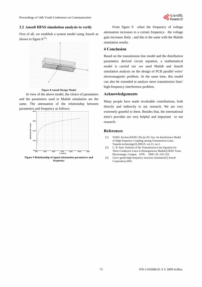
3.2 Ansoft HFSS simulation analysis to verify From figure 9 when the frequency of voltage
attenuation increases to a certain frequency,the voltage
gain increases flatly , and this is the same with the Matlab
simulation results.
First of all, we establish a system model using Ansoft as
shown in figure 8 [3]:
4 Conclusion Based on the transmission line model and the distribution
parameters derived circuit equation, a mathematical
model is carried out .we used Matlab and Ansoft
simulation analysis on the design of PCB parallel wires’
electromagnetic problem. At the same time, this model
can also be extended to analyze more transmission lines’
high-frequency interference problem. Figure 8 Ansoft Design Model
Acknowledgements In view of the above model, the choice of parameters
and the parameters used in Matlab simulation are the
same. The attenuation of the relationship between
parameters and frequency as follows:
Many people have made invaluable contributions, both
directly and indirectly to my research. We are very
extremely grateful to them. Besides that, the international
item’s provides are very helpful and important to our
research.
References [1] YANG Jin-hou,WANG Zhi-jie,XU Jun. An Interference Model
of High-frequency Coupling among Transmission Lines. Torpedo technology[J],2005/9, vol.13, no.3,
[2] C. R. Paul. Solution of the Transmission-Line Equation for Three-Conductor Lines in Homogeneous Media[J].IEEE Trans. Electromagn. Compat,1978, EMC-20: 216~222.
Figure 9 Relationship of signal attenuation parameters and frequency
[3] User's guide-high frequency structure simulator[Z].Ansoft Corporation,2005.
73
Proceedings of 14th Youth Conference on Communication
978-1-935068-01-3 © 2009 SciRes.


![PCB Via Analysis in Microwave Simulation Model · high-frequency signal than the former.Fig.3 shows the ... User's guide-high frequency structure simulator [Z].Ansoft Cor-poration,2005,P143-163](https://img.pdfslide.us/doc/110x75/5e916474db252c24e84ff83a/pcb-via-analysis-in-microwave-simulation-model-high-frequency-signal-than-the-shows.jpg)