Embed Size (px)
Citation preview

The Alphabet soup of
IPC Specifications
340 Raleigh Street
Holly Springs, NC 27540
http://www.circuittechnology.com
(919) 552 3434

About the IPC
� IPC-the electronics industry standard
�Founded in 1957 as the “Institute of Printed
Circuits”
�Lobbying, research, standards developement
�Relevant/current training for electronics
companies that make them more competitive
in the global market
�“Portable” certification that is a marketable
skill for the individual
�Replacing most military spec’s

The first IPC meeting-1957

PCB Assembly Specifications:
� IPC-7711/7721B
� IPC-A- 610E
� IPC/WHMA-A-620B
� IPC-J-STD-001E
� IPC-A-600H
� All are available in a CIS and a CIT level
� All differentiate class 1, 2, 3 and Space

IPC 7711/7721
� Rework and Repair of PCB’s
� Operator course modularized
� Lead Free Criteria included
� 90% hands-on component removal,
replacement and laminate repair

7711/7721 Modules
� 1-Common procedures
� 2-Wire splicing
� 3-TH rework
� 4-SMT chip and MELF soldering & removal
� 5-SOT & SOIC soldering & removal
� 6-PLCC & QFP soldering & removal (0.020”)
� 7-PCB repair (TH & SMT surface)
� 8-Conformal coat repair
� 9-PCB repair(internal)

Procedures of IPC-7711B Removal
� Procedure 3.3.1, Chip Component Removal -
Bifurcated Tip
� Procedure 3.3.2, Chip Component Removal -
Tweezer Method
� 3.3.3, Chip Component Removal - Procedure
Hot Air Method

3.3.1 Chip Component Removal –
Bifurcated Tip
Figure 1: Apply Flux Figure 2: Tin Tips Figure 3: Position
Tip
Figure 4: Melt All
Joints
Figure 5: Lift
Component

EQUIPMENT REQUIRED
Soldering system
Chip removal tip
Soldering handpiece
OPTIONAL EQUIPMENT
Tweezers
Controllable preheater
MATERIALS
Flux-cored solder
Flux
Cleaner
Product Class: R,F,W,C
Skill Level: Intermediate
Level of Conformance: High

� PROCEDURE
� 1. Remove conformal coating (if any) and clean work area of any
� contamination, oxides or residues.
� 2. Install the chip removal tip into the soldering handpiece.
� 3. Start with tip temperature of approximately 315°C and change
� as necessary.
� 4. Apply flux to all lead/land areas. (See Figure 1.)
� 5. Remove old solder from tip and thermal shock with a damp
� sponge.
� 6. Apply solder to inside of tip forming a crown. (See Figure 2.)
� 7. Lower tip over component until tip contacts solder joints. (See
� Figure 3.)
� 8. Confirm solder melt and lift component from PWB. (See Figures
� 4 & 5.) (Surface tension of the tip should lift the component from
� the board. If this does not occur, use of tweezers to lift the
� component is optional.)
Product Class: R,F,W,C
Skill Level: Intermediate
Level of Conformance: High

Procedure Continued:
NOTE: Chip components may have adhesive between the body and the board. If adhesive is used, it may be necessary to slightly turn the component to allow the component to be removed from the board. This must
only be accomplished after complete solder melt to prevent damage.
� 9. Release component from tip by wiping on a heat resistant
� surface.
� 10. Re-tin tip with solder.
� 11. Prepare lands for component replacement.
Product Class: R,F,W,C
Skill Level: Intermediate
Level of Conformance: High

SMT drag solder video


IPC 610
� Workmanship standards and inspection criterion
� Accept / Reject criteria for all 3 classes
� No hands-on, all soft skills
� Operator (CIS) modularized
� Includes lead free criteria

610 Modules
� 1-Common procedures
� 2-Documents and handling
� 3-Hardware installation
� 4-Soldering
� 5-Terminal connections
� 6-PTH
� 7-SMT
� 8-Component damage and PCB assemblies
� 9-Solderless wire wrap

8.2.2.3 CHIP COMPONENTS
END JOINT WIDTH
© 2005, IPC, Bannockburn, IL All rights
reserved. For use only in IPC Training
Programs leading to Official IPC
Certification
Figure 8-20
Acceptable – Class 3
50% 75%50%5 Figure 8-19
Acceptable - Class 1, 2
Note Pass for 3side of the solder
fillet.
Note Pass for 1&2owest side of the
solder fillet.

8.2.2.3 CHIP COMPONENTS
END JOINT WIDTH
© 2005, IPC, Bannockburn, IL All rights
reserved. For use only in IPC Training
Programs leading to Official IPC
Certification
Figure 8-22

8.2.2.41 CHIP COMPONENTS
SIDE JOINT LENGTH
© 2005, IPC, Bannockburn, IL All rights
reserved. For use only in IPC Training
Programs leading to Official IPC
Certification
Figure 8-23
Target – Class 1, 2, 3
Note 3. Wetting is evident.

8.2.2.6 CHIP COMPONENTS
MINIMUM FILLET HEIGHT
© 2005, IPC, Bannockburn, IL All rights
reserved. For use only in IPC Training
Programs leading to Official IPC
Certification
Figure 8-26
Acceptable – Class 1, 2, 3
Note 3. Wetting is evident.
Note 6. Designs with via in pad may
preclude meeting these criteria.
Solder acceptance criteria should be
defined between the user and the
manufacturer.
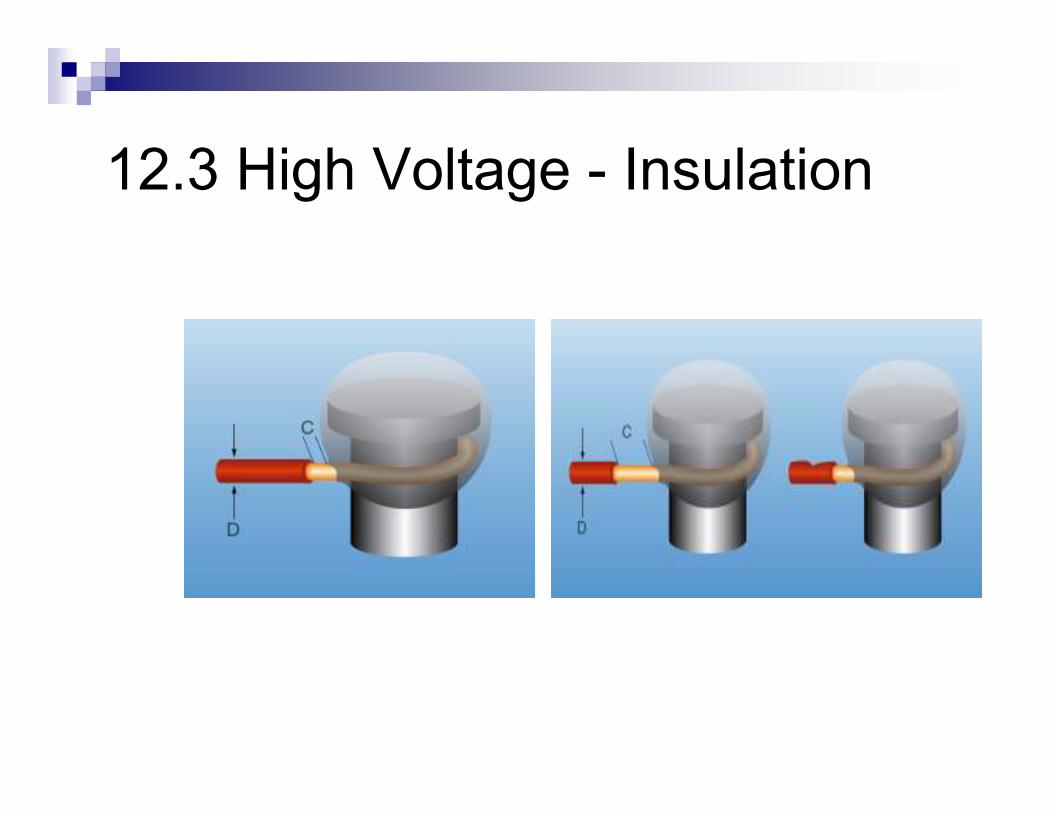
12.3 High Voltage - Insulation
Figure 12-11
Acceptable – Class 1, 2, 3
Figure 12-12
Defect – Class 1, 2, 3
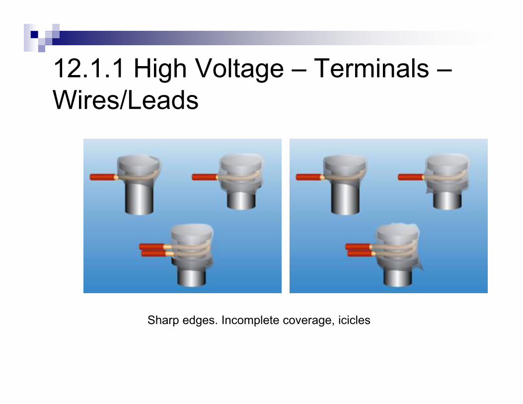
12.1.1 High Voltage – Terminals –
Wires/Leads
Figure 12-4
Defect– Class 1, 2, 3Sharp edges. Incomplete coverage, icicles

Review Questions
1. A high voltage terminal with no evidence of sharp edges, solder points, icicles, inclusions or wire strands is ____________,
A. Target – Class 1,2,3
B. Acceptable – Class 1,Process Indicator 2, 3
C. Defect – Class 1,2,3
D. Process Indicator – Class 1, Defect –Class 2, 3
A, Page 12-2, Clause 12.1.1

IPC/WHMA-A-620A
� Requirements and Acceptance for
Cable and Wire Harness Assemblies

620 Modules
� 1-Policies and procedures
� 2-Crimp terminations
� 3-Soldered terminations
� 4-Connectorization
� 5-Splices
� 6-Marking & labeling
� 7-Coaxial and twinaxial cable assemblies
� 8-Solderless wire wrap

8.2.1 Crimped Splices - Barrel
(Please use poll to answer)
Target - Class 1,2,3
• Wire insulation is flush against end of barrel splice (A).
• Bare wire ends are flush with barrel splice, bellmouth is evident (B).
• Crimp is centered and properly formed to retain wires (C).
• Barrel splice is not cracked.

8.2.1 Crimped Splices - Barrel
Acceptable - Class 1,2,3
• Wire insulation gap is within two wire diameters (A).
• Bare wire end is less than flush, but is visible and included in crimp indentation (B).
• Crimp slightly offset but properly formed, bellmouth is evident (C).
• Barrel splice is not cracked.
• Does not violate minimum electrical clearance.

IPC J-STD-001
� Process Control-Materials, Methods and
Verification Criteria
� 80% book 20% hands-on
� Soldering thru hole, SMT, terminals and
wires-very general
� CIS Modularized
� Refers to J-002-006

J-Standard supporting Documents
� 002-Solderability requirements-terminals
� 003-Solderability requirements-PCB’s
� 004-Requirements for soldering flux
� 005-Requirements for solder paste
� 006-Requirements for solder alloys
� 020-MSD classifications
J Standard Modules
� 1-Common procedures
� 2-Wires and terminals
� 3-PTH
� 4-SMT
� 5-Inspection
� 6-Space addendum

Table 7-7 Flat, Ribbon, ‘‘L,’’ and Gull
Wing LeadsFeature Feature Feature Feature Dim. Dim. Dim. Dim. Class 1 Class 1 Class 1 Class 1 Class 2 Class 2 Class 2 Class 2 Class 3 Class 3 Class 3 Class 3
Maximum Side Overhang
A
50% (W) or 0.5 mm [0.02 in],
whichever is less; Note 1
25% (W) or 0.5 mm [0.02 in], whichever is
less; Note 1
Figure 7- 7
Note 1. Does not violate minimum electrical clearance.

Table 7-7 Flat, Ribbon, ‘‘L,’’ and Gull
Wing Leads
Feature Feature Feature Feature Dim. Dim. Dim. Dim. Class 1 Class 1 Class 1 Class 1 Class 2 Class 2 Class 2 Class 2 Class 3 Class 3 Class 3 Class 3
Minimum End Joint Width
C 50%(W) 75%(W)
Figure 7- 7

Gull Wing Installation
Figure 1: Position
Component
Figure 2: Tack Lead Figure 3: Flux
Leads
Figure 4: Fill Tip Figure 5: Solder
Component
M5-18


IPC-600
� Acceptability of printed boards

600 modules
� 1-Policies and procedures
� 2-Externally observable characteristics
� 3-Internally observable characteristics
� 4-Miscellaneous and cleanliness
� 5-Question and answer period
� 6-Exam and exam review

2.3.1 Measling
Microsectioning not required as this is an externally observable requirement
A
1, 2, 3

2.3.2 Crazing
Microsectioning not required as this is an externally observable requirement
T A 1, 2, 3 N

2.3.4 Foreign Inclusions
T
N
A 1, 2, 3

1.3 Example
� Delamination
� Some attributes have both externally
observable and internally observable
requirements.
M1-39

Pop quiz: This laminate imperfection meets
which class requirements?
A. Class 1, only
B. Classes 1 and 2
C. Classes 1, 2 and 3
D. None of the above
R2-40
Answer: DRef: 2.3.3
Delamination/Blisters

Question 2: The plated hole condition is
acceptable for which class(es) of product?
A. Class 1
B. Classes 1 and 2
C. Class 2
D. Classes 2 and 3
R2-41
Answer: ARef: 2.10.3 External Annular
Ring – Supported Holes

All spec’s are related
J standard
620610
7711 600

Other IPC documents
� DRM’s
� “The seven sins of soldering”
� J-0033-handling of MSD’s
� CH-65B-cleaning PCB’s
� 7525-Stencil design guidelines
� 7095-BGA’s
� T-50-Terms and definitions
� Many other documents, industry reports etc.

Why Invest in Training?
� Industry recognized certification to show
your dedication to quality
� Increase throughput and reliability
� May be required (mil, med, auto, ISO)
� Employee retention
� Increase first pass yield
� Decrease defects
� Enhance your bottom line