Embed Size (px)
Citation preview
TGA4533-SM K-Band Power Amplifier
Preliminary Data Sheet: Rev - 02/09/2011 - 1 of 14 - Disclaimer: Subject to change without notice
© 2011 TriQuint Semiconductor, Inc. Connecting the Digital World to the Global Network®
Applications
• Point-to-Point Radio
• K-Band Sat-Com
QFN 4x4 mm 20L
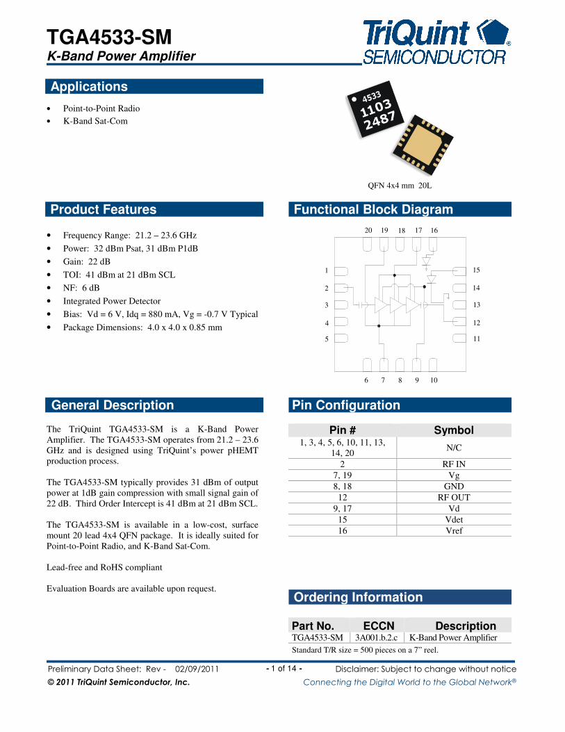
Product Features Functional Block Diagram
• Frequency Range: 21.2 – 23.6 GHz
• Power: 32 dBm Psat, 31 dBm P1dB
• Gain: 22 dB
• TOI: 41 dBm at 21 dBm SCL
• NF: 6 dB
• Integrated Power Detector
• Bias: Vd = 6 V, Idq = 880 mA, Vg = -0.7 V Typical
• Package Dimensions: 4.0 x 4.0 x 0.85 mm
20 19
14
109
11
12
13
1617
15
18
2
5
4
3
6 7 8
1
General Description Pin Configuration
The TriQuint TGA4533-SM is a K-Band Power
Amplifier. The TGA4533-SM operates from 21.2 – 23.6
GHz and is designed using TriQuint’s power pHEMT
production process.
The TGA4533-SM typically provides 31 dBm of output
power at 1dB gain compression with small signal gain of
22 dB. Third Order Intercept is 41 dBm at 21 dBm SCL.
The TGA4533-SM is available in a low-cost, surface
mount 20 lead 4x4 QFN package. It is ideally suited for
Point-to-Point Radio, and K-Band Sat-Com.
Lead-free and RoHS compliant
Evaluation Boards are available upon request.
Pin # Symbol 1, 3, 4, 5, 6, 10, 11, 13,
14, 20 N/C
2 RF IN
7, 19 Vg
8, 18 GND
12 RF OUT
9, 17 Vd
15 Vdet
16 Vref
Ordering Information
Part No. ECCN Description TGA4533-SM 3A001.b.2.c K-Band Power Amplifier
Standard T/R size = 500 pieces on a 7” reel.
TGA4533-SM K-Band Power Amplifier
Preliminary Data Sheet: Rev - 02/09/2011 - 2 of 14 - Disclaimer: Subject to change without notice
© 2011 TriQuint Semiconductor, Inc. Connecting the Digital World to the Global Network®
Specifications
Absolute Maximum Ratings
Parameter Rating Drain Voltage,Vd +6.5 V
Gate Voltage,Vg -3 to 0 V
Drain to Gate Voltage, Vd – Vg 10 V
Drain Current, Id 2 A
Gate Current, Ig -8.8 to 113 mA
Power Dissipation, Pdiss 12.7 W
RF Input Power, CW, T = 25ºC 26 dBm
Channel Temperature, Tch 200 oC
Mounting Temperature (30
Seconds)
260 oC
Storage Temperature -40 to 150 oC
Operation of this device outside the parameter ranges given
above may cause permanent damage. These are stress
ratings only, and functional operation of the device at these
conditions is not implied.
Recommended Operating Conditions
Parameter Min Typical Max Units Vd 6 V
Idq 880 mA
Id_drive (Under RF
Drive) 1300 mA
Vg -0.7 V
Electrical specifications are measured at specified test conditions.
Specifications are not guaranteed over all recommended operating
conditions.
Electrical Specifications
Test conditions unless otherwise noted: 25 ºC, Vd = 6 V, Idq = 880 mA, Vg = -0.7 V Typical.
Parameter Min Typical Max Units Operational Frequency Range 21.2 23.6 GHz
Gain 22 dB
Input Return Loss, IRL 10 dB
Output Return Loss, ORL 10 dB
Output Power @ Saturation, Psat 32 dBm
Output Power @ 1dB Gain Compression, P1dB 31 dBm
Output Third Order Intercept, TOI 41 dBm
Noise Figure, NF 6 dB
Gain Temperature Coefficient -0.025 dB/°C
Power Temperature Coefficient -0.015 dB/°C
TGA4533-SM K-Band Power Amplifier
Preliminary Data Sheet: Rev - 02/09/2011 - 3 of 14 - Disclaimer: Subject to change without notice
© 2011 TriQuint Semiconductor, Inc. Connecting the Digital World to the Global Network®
Specifications (cont.)
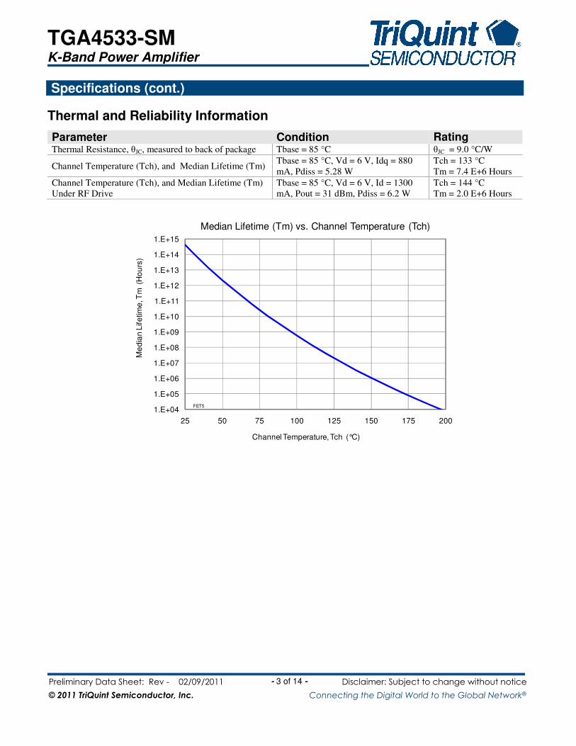
Thermal and Reliability Information
Parameter Condition Rating Thermal Resistance, θJC, measured to back of package Tbase = 85 °C θJC = 9.0 °C/W
Channel Temperature (Tch), and Median Lifetime (Tm) Tbase = 85 °C, Vd = 6 V, Idq = 880
mA, Pdiss = 5.28 W
Tch = 133 °C
Tm = 7.4 E+6 Hours
Channel Temperature (Tch), and Median Lifetime (Tm)
Under RF Drive
Tbase = 85 °C, Vd = 6 V, Id = 1300
mA, Pout = 31 dBm, Pdiss = 6.2 W
Tch = 144 °C
Tm = 2.0 E+6 Hours
1.E+04
1.E+05
1.E+06
1.E+07
1.E+08
1.E+09
1.E+10
1.E+11
1.E+12
1.E+13
1.E+14
1.E+15
25 50 75 100 125 150 175 200
Me
dia
n L
ife
time
, Tm
(H
ou
rs)
Channel Temperature, Tch (°C)
Median Lifetime (Tm) vs. Channel Temperature (Tch)
FET5
TGA4533-SM K-Band Power Amplifier
Preliminary Data Sheet: Rev - 02/09/2011 - 4 of 14 - Disclaimer: Subject to change without notice
© 2011 TriQuint Semiconductor, Inc. Connecting the Digital World to the Global Network®
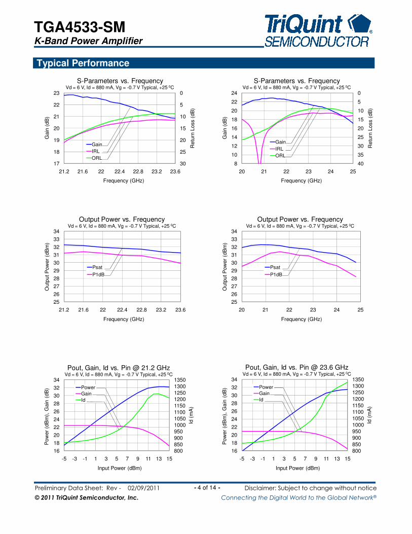
Typical Performance
25
26
27
28
29
30
31
32
33
34
21.2 21.6 22 22.4 22.8 23.2 23.6
Outp
ut P
ow
er
(dB
m)
Frequency (GHz)
Output Power vs. FrequencyVd = 6 V, Id = 880 mA, Vg = -0.7 V Typical, +25 0C
Psat
P1dB
25
26
27
28
29
30
31
32
33
34
20 21 22 23 24 25
Outp
ut P
ow
er
(dB
m)
Frequency (GHz)
Output Power vs. FrequencyVd = 6 V, Id = 880 mA, Vg = -0.7 V Typical, +25 0C
Psat
P1dB
800
850
900
950
1000
1050
1100
1150
1200
1250
1300
1350
16
18
20
22
24
26
28
30
32
34
-5 -3 -1 1 3 5 7 9 11 13 15
Id (
mA
)
Pow
er
(dB
m),
Gain
(dB
)
Input Power (dBm)
Pout, Gain, Id vs. Pin @ 21.2 GHzVd = 6 V, Id = 880 mA, Vg = -0.7 V Typical, +25 0C
Power
Gain
Id
800
850
900
950
1000
1050
1100
1150
1200
1250
1300
1350
16
18
20
22
24
26
28
30
32
34
-5 -3 -1 1 3 5 7 9 11 13 15
Id (
mA
)
Pow
er
(dB
m),
Gain
(dB
)
Input Power (dBm)
Pout, Gain, Id vs. Pin @ 23.6 GHzVd = 6 V, Id = 880 mA, Vg = -0.7 V Typical, +25 0C
Power
Gain
Id
0
5
10
15
20
25
3017
18
19
20
21
22
23
21.2 21.6 22 22.4 22.8 23.2 23.6
Retu
rn L
oss (
dB
)
Gain
(dB
)
Frequency (GHz)
S-Parameters vs. FrequencyVd = 6 V, Id = 880 mA, Vg = -0.7 V Typical, +25 0C
Gain
IRL
ORL
0
5
10
15
20
25
30
35
408
10
12
14
16
18
20
22
24
20 21 22 23 24 25
Retu
rn L
oss (
dB
)
Gain
(dB
)
Frequency (GHz)
S-Parameters vs. FrequencyVd = 6 V, Id = 880 mA, Vg = -0.7 V Typical, +25 0C
Gain
IRL
ORL
TGA4533-SM K-Band Power Amplifier
Preliminary Data Sheet: Rev - 02/09/2011 - 5 of 14 - Disclaimer: Subject to change without notice
© 2011 TriQuint Semiconductor, Inc. Connecting the Digital World to the Global Network®
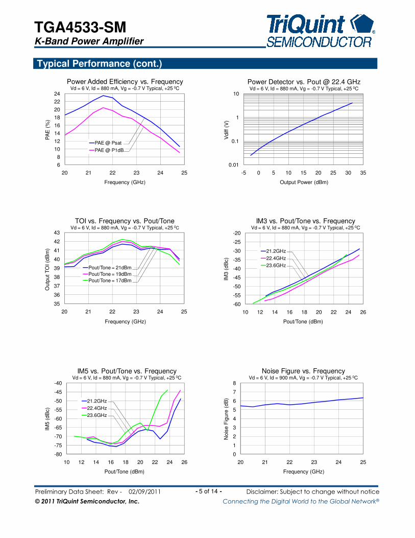
Typical Performance (cont.)
6
8
10
12
14
16
18
20
22
24
20 21 22 23 24 25
PA
E (
%)
Frequency (GHz)
Power Added Efficiency vs. FrequencyVd = 6 V, Id = 880 mA, Vg = -0.7 V Typical, +25 0C
PAE @ Psat
PAE @ P1dB
0.01
0.1
1
10
-5 0 5 10 15 20 25 30 35
Vdiff
(V
)
Output Power (dBm)
Power Detector vs. Pout @ 22.4 GHz Vd = 6 V, Id = 880 mA, Vg = -0.7 V Typical, +25 0C
35
36
37
38
39
40
41
42
43
20 21 22 23 24 25
Outp
ut T
OI (d
Bm
)
Frequency (GHz)
TOI vs. Frequency vs. Pout/ToneVd = 6 V, Id = 880 mA, Vg = -0.7 V Typical, +25 0C
Pout/Tone = 21dBm
Pout/Tone = 19dBm
Pout/Tone = 17dBm
-60
-55
-50
-45
-40
-35
-30
-25
-20
10 12 14 16 18 20 22 24 26
IM3 (
dB
c)
Pout/Tone (dBm)
IM3 vs. Pout/Tone vs. FrequencyVd = 6 V, Id = 880 mA, Vg = -0.7 V Typical, +25 0C
21.2GHz
22.4GHz
23.6GHz
-80
-75
-70
-65
-60
-55
-50
-45
-40
10 12 14 16 18 20 22 24 26
IM5 (
dB
c)
Pout/Tone (dBm)
IM5 vs. Pout/Tone vs. FrequencyVd = 6 V, Id = 880 mA, Vg = -0.7 V Typical, +25 0C
21.2GHz
22.4GHz
23.6GHz
0
1
2
3
4
5
6
7
8
20 21 22 23 24 25
Nois
e F
igure
(dB
)
Frequency (GHz)
Noise Figure vs. FrequencyVd = 6 V, Id = 900 mA, Vg = -0.7 V Typical, +25 0C
TGA4533-SM K-Band Power Amplifier
Preliminary Data Sheet: Rev - 02/09/2011 - 6 of 14 - Disclaimer: Subject to change without notice
© 2011 TriQuint Semiconductor, Inc. Connecting the Digital World to the Global Network®
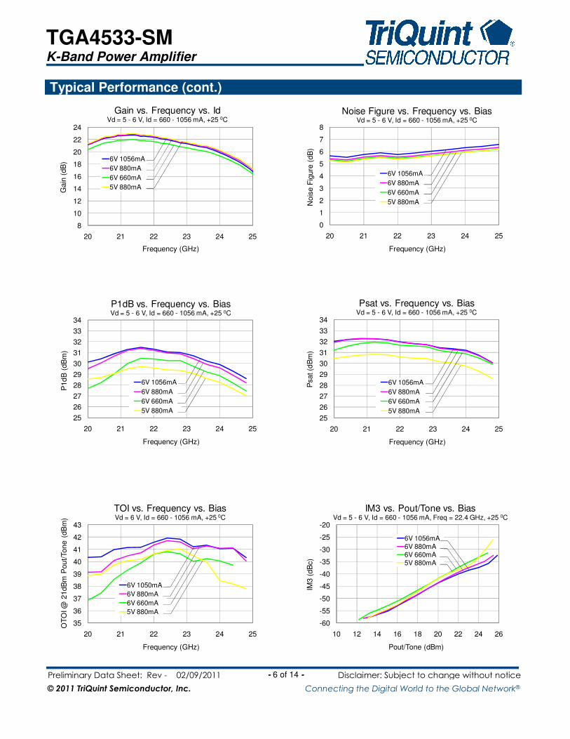
Typical Performance (cont.)
8
10
12
14
16
18
20
22
24
20 21 22 23 24 25
Gain
(dB
)
Frequency (GHz)
Gain vs. Frequency vs. IdVd = 5 - 6 V, Id = 660 - 1056 mA, +25 0C
6V 1056mA
6V 880mA
6V 660mA
5V 880mA
0
1
2
3
4
5
6
7
8
20 21 22 23 24 25
Nois
e F
igure
(dB
)
Frequency (GHz)
Noise Figure vs. Frequency vs. BiasVd = 5 - 6 V, Id = 660 - 1056 mA, +25 0C
6V 1056mA
6V 880mA
6V 660mA
5V 880mA
25
26
27
28
29
30
31
32
33
34
20 21 22 23 24 25
P1d
B (
dB
m)
Frequency (GHz)
P1dB vs. Frequency vs. BiasVd = 5 - 6 V, Id = 660 - 1056 mA, +25 0C
6V 1056mA
6V 880mA
6V 660mA
5V 880mA25
26
27
28
29
30
31
32
33
34
20 21 22 23 24 25
Psat (d
Bm
)
Frequency (GHz)
Psat vs. Frequency vs. BiasVd = 5 - 6 V, Id = 660 - 1056 mA, +25 0C
6V 1056mA
6V 880mA
6V 660mA
5V 880mA
35
36
37
38
39
40
41
42
43
20 21 22 23 24 25
OT
OI @
21dB
m P
out/Ton
e (
dB
m)
Frequency (GHz)
TOI vs. Frequency vs. BiasVd = 6 V, Id = 660 - 1056 mA, +25 0C
6V 1050mA
6V 880mA
6V 660mA
5V 880mA
-60
-55
-50
-45
-40
-35
-30
-25
-20
10 12 14 16 18 20 22 24 26
IM3 (
dB
c)
Pout/Tone (dBm)
IM3 vs. Pout/Tone vs. BiasVd = 5 - 6 V, Id = 660 - 1056 mA, Freq = 22.4 GHz, +25 0C
6V 1056mA6V 880mA6V 660mA5V 880mA
TGA4533-SM K-Band Power Amplifier
Preliminary Data Sheet: Rev - 02/09/2011 - 7 of 14 - Disclaimer: Subject to change without notice
© 2011 TriQuint Semiconductor, Inc. Connecting the Digital World to the Global Network®
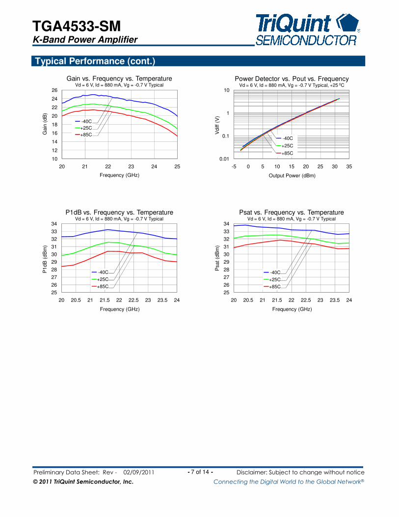
Typical Performance (cont.)
10
12
14
16
18
20
22
24
26
20 21 22 23 24 25
Gain
(d
B)
Frequency (GHz)
Gain vs. Frequency vs. TemperatureVd = 6 V, Id = 880 mA, Vg = -0.7 V Typical
-40C
+25C
+85C
0.01
0.1
1
10
-5 0 5 10 15 20 25 30 35
Vdiff
(V
)
Output Power (dBm)
Power Detector vs. Pout vs. Frequency Vd = 6 V, Id = 880 mA, Vg = -0.7 V Typical, +25 0C
-40C
+25C
+85C
25
26
27
28
29
30
31
32
33
34
20 20.5 21 21.5 22 22.5 23 23.5 24
Psat (d
Bm
)
Frequency (GHz)
Psat vs. Frequency vs. TemperatureVd = 6 V, Id = 880 mA, Vg = -0.7 V Typical
-40C
+25C
+85C
25
26
27
28
29
30
31
32
33
34
20 20.5 21 21.5 22 22.5 23 23.5 24
P1d
B (
dB
m)
Frequency (GHz)
P1dB vs. Frequency vs. TemperatureVd = 6 V, Id = 880 mA, Vg = -0.7 V Typical
-40C
+25C
+85C
TGA4533-SM K-Band Power Amplifier
Preliminary Data Sheet: Rev - 02/09/2011 - 8 of 14 - Disclaimer: Subject to change without notice
© 2011 TriQuint Semiconductor, Inc. Connecting the Digital World to the Global Network®
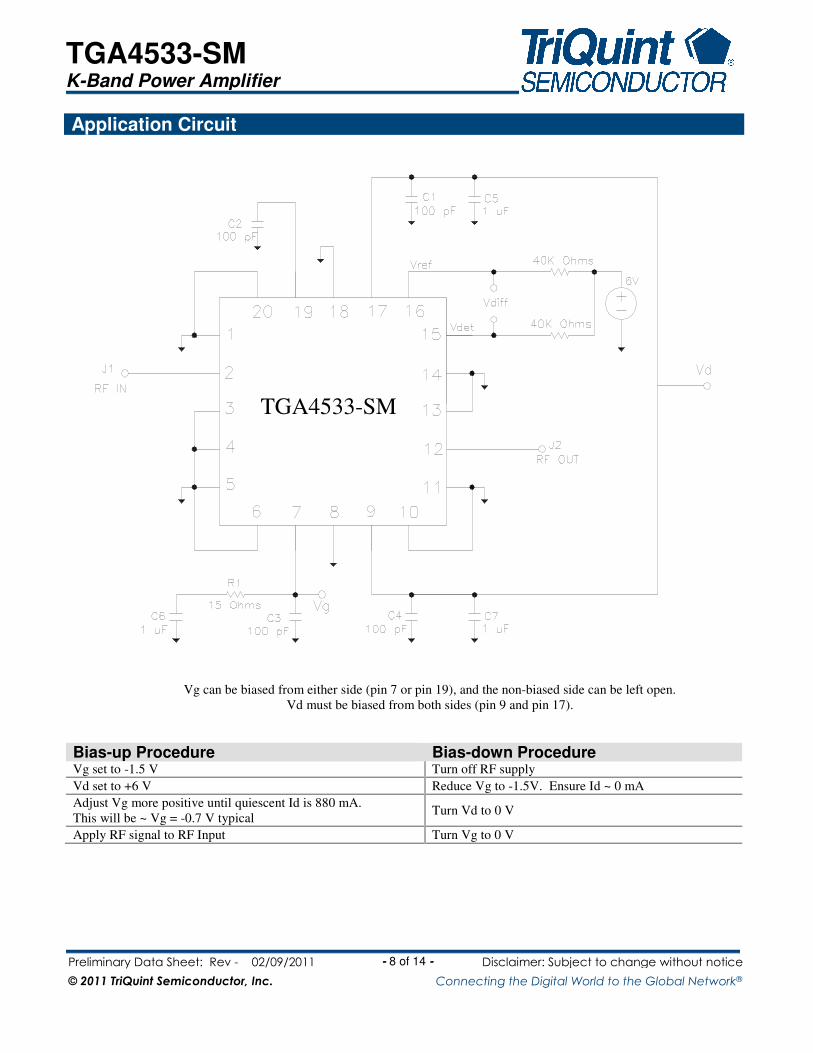
Application Circuit
TGA4533-SM
Vg can be biased from either side (pin 7 or pin 19), and the non-biased side can be left open.
Vd must be biased from both sides (pin 9 and pin 17).
Bias-up Procedure Bias-down Procedure Vg set to -1.5 V Turn off RF supply
Vd set to +6 V Reduce Vg to -1.5V. Ensure Id ~ 0 mA
Adjust Vg more positive until quiescent Id is 880 mA.
This will be ~ Vg = -0.7 V typical Turn Vd to 0 V
Apply RF signal to RF Input Turn Vg to 0 V
TGA4533-SM K-Band Power Amplifier
Preliminary Data Sheet: Rev - 02/09/2011 - 9 of 14 - Disclaimer: Subject to change without notice
© 2011 TriQuint Semiconductor, Inc. Connecting the Digital World to the Global Network®
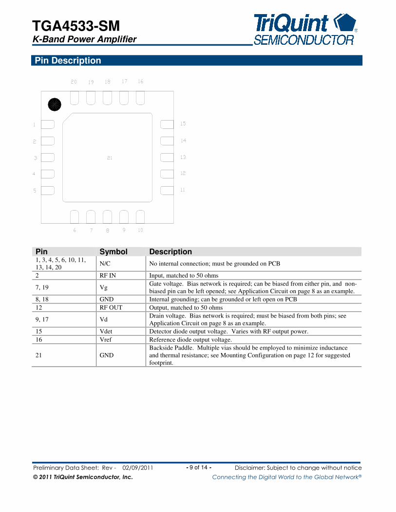
Pin Description
Pin Symbol Description 1, 3, 4, 5, 6, 10, 11,
13, 14, 20 N/C No internal connection; must be grounded on PCB
2 RF IN Input, matched to 50 ohms
7, 19 Vg Gate voltage. Bias network is required; can be biased from either pin, and non-
biased pin can be left opened; see Application Circuit on page 8 as an example.
8, 18 GND Internal grounding; can be grounded or left open on PCB
12 RF OUT Output, matched to 50 ohms
9, 17 Vd Drain voltage. Bias network is required; must be biased from both pins; see
Application Circuit on page 8 as an example.
15 Vdet Detector diode output voltage. Varies with RF output power.
16 Vref Reference diode output voltage.
21 GND
Backside Paddle. Multiple vias should be employed to minimize inductance
and thermal resistance; see Mounting Configuration on page 12 for suggested
footprint.
TGA4533-SM K-Band Power Amplifier
Preliminary Data Sheet: Rev - 02/09/2011 - 10 of 14 - Disclaimer: Subject to change without notice
© 2011 TriQuint Semiconductor, Inc. Connecting the Digital World to the Global Network®
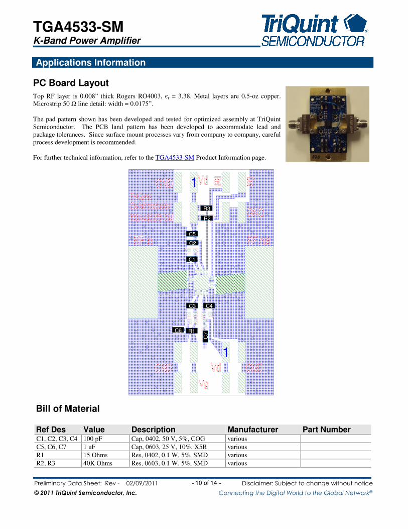
Applications Information
PC Board Layout
Top RF layer is 0.008” thick Rogers RO4003, єr = 3.38. Metal layers are 0.5-oz copper.
Microstrip 50 Ω line detail: width = 0.0175”.
The pad pattern shown has been developed and tested for optimized assembly at TriQuint
Semiconductor. The PCB land pattern has been developed to accommodate lead and
package tolerances. Since surface mount processes vary from company to company, careful
process development is recommended.
For further technical information, refer to the TGA4533-SM Product Information page.
Bill of Material
Ref Des Value Description Manufacturer Part Number C1, C2, C3, C4 100 pF Cap, 0402, 50 V, 5%, COG various
C5, C6, C7 1 uF Cap, 0603, 25 V, 10%, X5R various
R1 15 Ohms Res, 0402, 0.1 W, 5%, SMD various
R2, R3 40K Ohms Res, 0603, 0.1 W, 5%, SMD various
C1
C3 C4
C2
C7
C5
C6 R1
R3
R2
1
1
TGA4533-SM K-Band Power Amplifier
Preliminary Data Sheet: Rev - 02/09/2011 - 11 of 14 - Disclaimer: Subject to change without notice
© 2011 TriQuint Semiconductor, Inc. Connecting the Digital World to the Global Network®
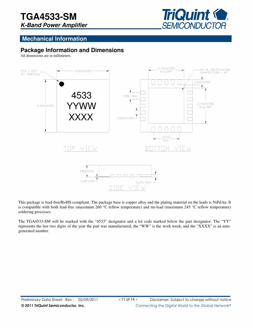
Mechanical Information
Package Information and Dimensions All dimensions are in millimeters.
4533YYWW
XXXX
This package is lead-free/RoHS-compliant. The package base is copper alloy and the plating material on the leads is NiPdAu. It
is compatible with both lead-free (maximum 260 °C reflow temperature) and tin-lead (maximum 245 °C reflow temperature)
soldering processes.
The TGA4533-SM will be marked with the “4533” designator and a lot code marked below the part designator. The “YY”
represents the last two digits of the year the part was manufactured, the “WW” is the work week, and the “XXXX” is an auto-
generated number.
TGA4533-SM K-Band Power Amplifier
Preliminary Data Sheet: Rev - 02/09/2011 - 12 of 14 - Disclaimer: Subject to change without notice
© 2011 TriQuint Semiconductor, Inc. Connecting the Digital World to the Global Network®
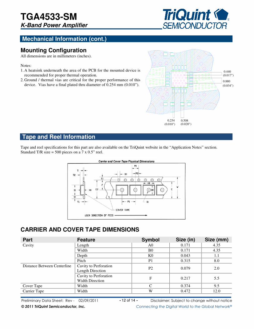
0.440
0.880
0.254 0.508(0.010") (0.020")
(0.017")
(0.034")
Mechanical Information (cont.)
Mounting Configuration All dimensions are in millimeters (inches).
Notes:
1. A heatsink underneath the area of the PCB for the mounted device is
recommended for proper thermal operation.
2. Ground / thermal vias are critical for the proper performance of this
device. Vias have a final plated thru diameter of 0.254 mm (0.010”).
Tape and Reel Information
Tape and reel specifications for this part are also available on the TriQuint website in the “Application Notes” section.
Standard T/R size = 500 pieces on a 7 x 0.5” reel.
CARRIER AND COVER TAPE DIMENSIONS
Part Feature Symbol Size (in) Size (mm) Cavity Length A0 0.171 4.35
Width B0 0.171 4.35
Depth K0 0.043 1.1
Pitch P1 0.315 8.0
Distance Between Centerline Cavity to Perforation
Length Direction P2 0.079 2.0
Cavity to Perforation
Width Direction F 0.217 5.5
Cover Tape Width C 0.374 9.5
Carrier Tape Width W 0.472 12.0
TGA4533-SM K-Band Power Amplifier
Preliminary Data Sheet: Rev - 02/09/2011 - 13 of 14 - Disclaimer: Subject to change without notice
© 2011 TriQuint Semiconductor, Inc. Connecting the Digital World to the Global Network®
Product Compliance Information
ESD Information
ESD Rating: Class 1A
Value: ≥ 250V and ≤ 500V
Test: Human Body Model (HBM)
Standard: JEDEC Standard JESD22-A114
Solderability
Compatible with the latest version of J-STD-020, Lead
free solder, 260°
This part is compliant with EU 2002/95/EC RoHS
directive (Restrictions on the Use of Certain Hazardous
Substances in Electrical and Electronic Equipment).
This product also has the following attributes:
• Lead Free
• Halogen Free (Chlorine, Bromine)
• Antimony Free
• TBBP-A (C15H12Br402) Free
• PFOS Free
• SVHC Free
MSL Rating
Level TBD at +260 °C convection reflow
The part is rated Moisture Sensitivity Level TBD at 260°C per
JEDEC standard IPC/JEDEC J-STD-020.
ECCN
US Department of Commerce 3A001.b.2.c
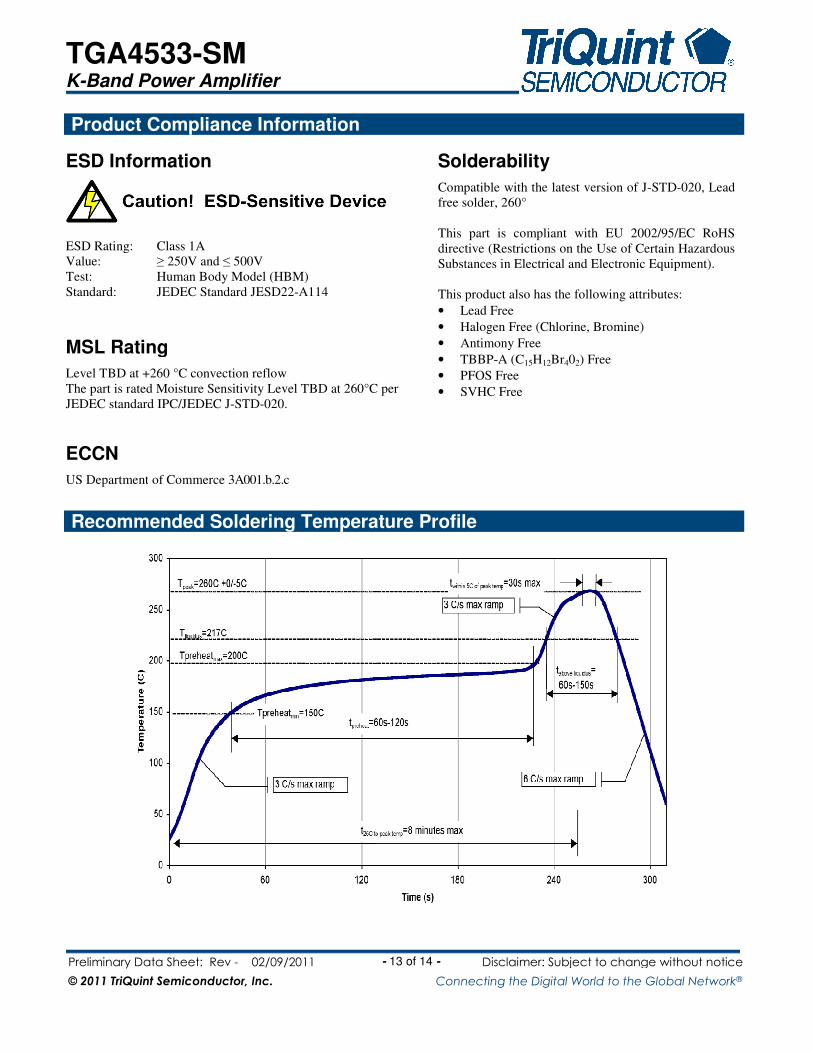
Recommended Soldering Temperature Profile
TGA4533-SM K-Band Power Amplifier
Preliminary Data Sheet: Rev - 02/09/2011 - 14 of 14 - Disclaimer: Subject to change without notice
© 2011 TriQuint Semiconductor, Inc. Connecting the Digital World to the Global Network®
Contact Information
For the latest specifications, additional product information, worldwide sales and distribution locations, and information about
TriQuint:
Web: www.triquint.com Tel: +1.972.994.8465 Email: [email protected] Fax: +1.972.994.8504 For technical questions and application information: Email: [email protected]
Important Notice
The information contained herein is believed to be reliable. TriQuint makes no warranties regarding the information contained
herein. TriQuint assumes no responsibility or liability whatsoever for any of the information contained herein. TriQuint
assumes no responsibility or liability whatsoever for the use of the information contained herein. The information contained
herein is provided "AS IS, WHERE IS" and with all faults, and the entire risk associated with such information is entirely with
the user. All information contained herein is subject to change without notice. Customers should obtain and verify the latest
relevant information before placing orders for TriQuint products. The information contained herein or any use of such
information does not grant, explicitly or implicitly, to any party any patent rights, licenses, or any other intellectual property
rights, whether with regard to such information itself or anything described by such information.
TriQuint products are not warranted or authorized for use as critical components in medical, life-saving, or life-sustaining
applications, or other applications where a failure would reasonably be expected to cause severe personal injury or death.
Copyright © 2011 TriQuint Semiconductor, Inc. All rights reserved.