Embed Size (px)
Citation preview
TGA2599-SM 5 – 8 GHz 2W GaN Driver Amplifier
Data Sheet Rev C, April 2019 | Subject to change without notice - 1 of 14 - www.qorvo.com
Product Description Qorvo's TGA2599-SM is a packaged driver amplifier fabricated on Qorvo's QGaN25 0.25um GaN on SiC production process. The TGA2599-SM operates from 5.0 to 8.0GHz and provides 33 dBm of output power with 15 dB of large signal gain and 34 % power-added efficiency. Using GaN MMIC technology and plastic packaging, the TGA2599-SM provides a low cost driver solution that provides the added benefit of operating on the same voltage rail as the corresponding GaN HPA. It can also serve as the primary amplifier on lower power architectures.
The TGA2599 is offered in a small 4 x 4 mm plastic overmold QFN, fully matched to 50 ohms and includes integrated DC blocking caps on both RF ports allowing for simple system integration.
Product Features • Frequency Range: 5.0-8.0 GHz
• Small Signal Gain: 23 dB
• Saturated Power (CW): 33 dBm
• PAE (CW, @Pin = 18 dBm): 34%
• IM3: -25 dBc @ 26 dBm Pout • Bias: VD = 25 V, IDQ = 50 mA
• Package Dimensions: 4.0 x 4.0 x 0.85 mm
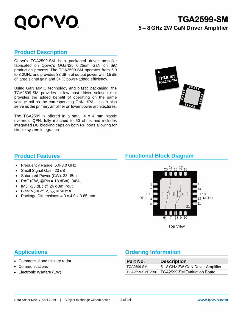
Functional Block Diagram
Top View
Ordering Information
Part No. Description TGA2599-SM 5 – 8 GHz 2W GaN Driver Amplifier
TGA2599-SMEVB01 TGA2599-SM Evaluation Board
Applications • Commercial and military radar
• Communications
• Electronic Warfare (EW)
1
6 8
19 17
3
RF In
13
RF Out
21
2
4
5
7 9 10
12
11
14
15
161820

TGA2599-SM 5 – 8 GHz 2W GaN Driver Amplifier
Data Sheet Rev C, April 2019 | Subject to change without notice - 2 of 14 - www.qorvo.com
Electrical Specifications Parameter Min Typ Max Units
Operational Frequency Range 5 8 GHz
Small Signal Gain 23 dB
Input Return Loss 17 dB
Output Return Loss 5 dB
Output Power (at Pin = 18 dBm) 33 dBm
Power Added Efficiency (at Pin = 18 dBm) 34 %
Test conditions unless otherwise noted: TBASE = +25 °C, VD = +25 V, IDQ= 50 mA, VG = -2.5V typical, CW Mode Data de-embedded to reference planes
Recommended Operating Conditions Parameter Min Typ Max Units
Drain Voltage (VD) 25 V
Drain Current (IDQ) 50 mA
Drain Current Under RF Drive (ID_DRIVE) See plots mA
Gate Voltage (VG) −2.5 V
Gate Current Under RF Drive (IG_DRIVE) See plots mA
Temperature (TBASE) −40 +85 °C
Electrical performance is measured under conditions noted in the electrical specifications table. Specifications are not guaranteed over all recommended operating conditions.

TGA2599-SM 5 – 8 GHz 2W GaN Driver Amplifier
Data Sheet Rev C, April 2019 | Subject to change without notice - 3 of 14 - www.qorvo.com
Thermal and Reliability Information
Parameter Values Units Conditions
Under Drive, Thermal Resistance (θJC) (1,2,3) 16.3 °C/W TBASE = 85 °C, VD = +25 V, CW
Freq = 8 GHz, ID_DRIVE = 250 mA
PIN = +18 dBm, POUT = +33 dBm, PDISS = 4.2 W Channel Temperature (TCH) 153.48 °C
Notes:
1. Thermal resistance is measured to package backside
2. Base or ambient temperature is 85 °C
3. Refer to the following document: GaN Device Channel Temperature, Thermal Resistance, and Reliability Estimates
Absolute Maximum Ratings Parameter Range / Value Units
Drain Voltage (VD) 40 V
Gate Voltage Range (VG) -8 to 0 V
Drain Current (ID1) 128 mA
Drain Current (ID2) 260 mA
Gate Current (IG1) at Tch = 200 °C 1.4 mA
Gate Current (IG2) at Tch = 200 °C 2.8 mA
Power Dissipation (PDISS), 85 °C 5.5 W
Input Power (PIN), CW, 50 Ω 30 dBm
Input Power (PIN), CW, VSWR 10:1 25 dBm
Mounting Temperature (30 Seconds) 260 °C
Storage Temperature -55 to 150 °C
Operation of this device outside the parameter ranges given above may cause permanent damage. These are stress ratings only, and functional operation of the device at these conditions is not implied. Extended application of Absolute Maximum Rating conditions to the device may reduce device reliability.

TGA2599-SM 5 – 8 GHz 2W GaN Driver Amplifier
Data Sheet Rev C, April 2019 | Subject to change without notice - 4 of 14 - www.qorvo.com
Performance Plots – Small Signal
Test conditions unless otherwise specified: VD = 25 V, IDQ = 50 mA, VG = -2.5 V Typical, CW, 25 °C
0
5
10
15
20
25
30
35
4 5 6 7 8 9 10 11 12
S2
1 (
dB
)
Frequency (GHz)
Gain vs. Freq. vs. Temp.
-40 °C
+25 °C
+85 °C
VD = 25 V, IDQ = 50 mA
0
5
10
15
20
25
30
35
4 5 6 7 8 9 10 11 12
S2
1 (
dB
)
Frequency (GHz)
Gain vs. Freq. vs. VD
20 V
25 V
30 V
IDQ = 50 mA, T = 25 C
-30
-25
-20
-15
-10
-5
0
4 5 6 7 8 9 10 11 12
S11
(d
B)
Frequency (GHz)
Input Return Loss vs. Freq. vs. Temp.
-40 °C
+25 °C
+85 °C
VD = 25 V, IDQ = 50 mA
-30
-25
-20
-15
-10
-5
0
4 5 6 7 8 9 10 11 12
S11
(d
B)
Frequency (GHz)
Input Return Loss vs. Freq. vs. VD
20 V
25 V
30 V
IDQ = 50 mA, T = 25 C
-30
-25
-20
-15
-10
-5
0
4 5 6 7 8 9 10 11 12
S2
2 (
dB
)
Frequency (GHz)
Output Return Loss vs. Freq. vs. Temp.
-40 °C
+25 °C
+85 °C
VD = 25 V, IDQ = 50 mA
-30
-25
-20
-15
-10
-5
0
4 5 6 7 8 9 10 11 12
S2
2 (
dB
)
Frequency (GHz)
Output Return Loss vs. Freq. vs. VD
20 V
25 V
30 V
IDQ = 50 mA, T = 25 C

TGA2599-SM 5 – 8 GHz 2W GaN Driver Amplifier
Data Sheet Rev C, April 2019 | Subject to change without notice - 5 of 14 - www.qorvo.com
Performance Plots – Small Signal
Test conditions unless otherwise specified: VD = 25 V, IDQ = 50 mA, VG = -2.5 V Typical, CW, 25 °C
0
5
10
15
20
25
30
35
4 5 6 7 8 9 10 11 12
S2
1 (
dB
)
Frequency (GHz)
Gain vs. Freq. vs. IDQ
50 mA
100 mA
150 mA
VD = 25 V, T = 25 C
-30
-25
-20
-15
-10
-5
0
4 5 6 7 8 9 10 11 12
S11
(d
B)
Frequency (GHz)
Input Return Loss vs. Freq. vs. IDQ
50 mA
100 mA
150 mA
VD = 25 V, T = 25 C
-30
-25
-20
-15
-10
-5
0
4 5 6 7 8 9 10 11 12
S2
2 (
dB
)
Frequency (GHz)
Output Return Loss vs. Freq. vs. IDQ
50 mA
100 mA
150 mA
VD = 25 V, T = 25 C

TGA2599-SM 5 – 8 GHz 2W GaN Driver Amplifier
Data Sheet Rev C, April 2019 | Subject to change without notice - 6 of 14 - www.qorvo.com
Performance Plots – Large Signal
Test conditions unless otherwise specified: VD = 25 V, IDQ = 50 mA, VG = -2.5 V Typical, CW, 25 °C
20
22
24
26
28
30
32
34
36
38
5 6 7 8 9 10 11 12
Ou
tpu
t P
ow
er
(dB
m)
Frequency (GHz)
Output Power vs. Frequency vs. Pin
13 dBm
15 dBm
17 dBm
19 dBm
21 dBm
23 dBm
VD = 25 V, IDQ = 50 mA, Temp. = 25 C
20
22
24
26
28
30
32
34
36
38
5 6 7 8 9 10 11 12
Ou
tpu
t P
ow
er
(dB
m)
Frequency (GHz)
Output Power vs. Frequency vs. Temp.
-40 °C
25 °C
85 °C
VD = 25 V, IDQ = 50 mA, Pin = 18 dBm
0
5
10
15
20
25
30
35
40
45
50
5 6 7 8 9 10 11 12
Po
we
r A
dd
ed
Eff. (%
)
Frequency (GHz)
Power Added Eff. vs. Freq. vs. Pin
13 dBm
15 dBm
17 dBm
19 dBm
21 dBm
23 dBm
VD = 25 V, IDQ = 50 mA, Temp. = 25 C
0
5
10
15
20
25
30
35
40
45
50
5 6 7 8 9 10 11 12
Po
we
r A
dd
ed
Eff. (%
)
Frequency (GHz)
Power Added Eff. vs. Freq. vs. Temp.
-40 °C
25 °C
85 °C
VD = 25 V, IDQ = 50 mA, Pin = 18 dBm
0
50
100
150
200
250
300
350
400
5 6 7 8 9 10 11 12
Dra
in C
urr
ent
(mA
)
Frequency (GHz)
Drain Current vs. Frequency vs. Pin
13 dBm
15 dBm
17 dBm
19 dBm
21 dBm
23 dBm
VD = 25 V, Temp. = 25 C
0
50
100
150
200
250
300
350
400
5 6 7 8 9 10 11 12
Dra
in C
urr
en
t (m
A)
Frequency (GHz)
Drain Current vs. Frequency vs. Temp.
-40 °C
25 °C
85 °C
VD = 25 V, Pin = 18 dBm

TGA2599-SM 5 – 8 GHz 2W GaN Driver Amplifier
Data Sheet Rev C, April 2019 | Subject to change without notice - 7 of 14 - www.qorvo.com
Performance Plots – Large Signal
Test conditions unless otherwise specified: VD = 25 V, IDQ = 50 mA, VG = -2.5 V Typical, CW, 25 °C
20
23
26
29
32
35
3 5 7 9 11 13 15 17 19 21 23
Outp
ut P
ow
er
(dB
m)
Input Power (dBm)
Output Power vs. Pin vs. Frequency
5.0 GHz
6.0 GHz
7.0 GHz
8.0 GHz
VD = 25 V, Temp. = 25 C
0
10
20
30
40
50
3 5 7 9 11 13 15 17 19 21 23
Pow
er A
dded E
ff. (%
)
Input Power (dBm)
Power Added Eff. vs. Pin vs. Frequency
5.0 GHz
6.0 GHz
7.0 GHz
8.0 GHz
VD = 25 V, Temp. = 25 C
20
23
26
29
32
35
3 5 7 9 11 13 15 17 19 21 23
Outp
ut P
ow
er
(dB
m)
Input Power (dBm)
Output Power vs. Pin vs. Temp.
-40 °C
25 °C
85 °C
VD = 25 V, Freq. = 5.0 GHz
0
5
10
15
20
25
30
35
40
45
50
3 5 7 9 11 13 15 17 19 21 23
Pow
er A
dded E
ff. (%
)
Input Power (dBm)
Power Added Eff. vs. Pin vs. Temp.
-40 °C
25 °C
85 °C
VD = 25 V, Freq. = 5.0 GHz
20
23
26
29
32
35
3 5 7 9 11 13 15 17 19 21 23
Outp
ut P
ow
er
(dB
m)
Input Power (dBm)
Output Power vs. Pin vs. Temp.
-40 °C
25 °C
85 °C
VD = 25 V, Freq. = 6.5 GHz
0
5
10
15
20
25
30
35
40
45
50
3 5 7 9 11 13 15 17 19 21 23
Pow
er A
dded E
ff. (%
)
Input Power (dBm)
Power Added Eff. vs. Pin vs. Temp.
-40 °C
25 °C
85 °C
VD = 25 V, Freq. = 6.5 GHz

TGA2599-SM 5 – 8 GHz 2W GaN Driver Amplifier
Data Sheet Rev C, April 2019 | Subject to change without notice - 8 of 14 - www.qorvo.com
Performance Plots – Large Signals
Test conditions unless otherwise specified: VD = 25 V, IDQ = 50 mA, VG = -2.5 V Typical, CW, 25 °C
20
23
26
29
32
35
3 5 7 9 11 13 15 17 19 21 23
Outp
ut P
ow
er
(dB
m)
Input Power (dBm)
Output Power vs. Pin vs. Temp.
-40 °C
25 °C
85 °C
VD = 25 V, Freq. = 8.0 GHz
0
5
10
15
20
25
30
35
40
45
50
3 5 7 9 11 13 15 17 19 21 23
Pow
er A
dded E
ff. (%
)
Input Power (dBm)
Power Added Eff. vs. Pin vs. Temp.
-40 °C
25 °C
85 °C
VD = 25 V, Freq. = 8.0 GHz
20
22
24
26
28
30
32
34
36
38
5 6 7 8 9 10 11 12
Ou
tpu
t P
ow
er
(dB
m)
Frequency (GHz)
Output Power vs. Frequency vs. VD
20 V
25 V
30 V
35 V
Pin = 18 dBm, IDQ = 50 mA, Temp. = 25 C
20
22
24
26
28
30
32
34
36
38
5 6 7 8 9 10 11 12
Ou
tpu
t P
ow
er
(dB
m)
Frequency (GHz)
Output Power vs. Frequency vs. ID
50 mA
100 mA
150 mA
Pin = 18 dBm, VD = 25 V, Temp. = 25 C
0
5
10
15
20
25
30
35
40
45
50
5 6 7 8 9 10 11 12
Po
we
r A
dd
ed
Eff. (%
)
Frequency (GHz)
Power Added Eff. vs. Frequency vs. VD
20 V
25 V
30 V
35 V
Pin = 18 dBm, IDQ = 50 mA, Temp. = 25 C
0
5
10
15
20
25
30
35
40
45
50
5 6 7 8 9 10 11 12
Po
we
r A
dd
ed
Eff. (%
)
Frequency (GHz)
Power Added Eff. vs. Frequency vs. ID
50 mA
100 mA
150 mA
Pin = 18 dBm, VD = 25 V, Temp. = 25 C
TGA2599-SM 5 – 8 GHz 2W GaN Driver Amplifier
Data Sheet Rev C, April 2019 | Subject to change without notice - 9 of 14 - www.qorvo.com
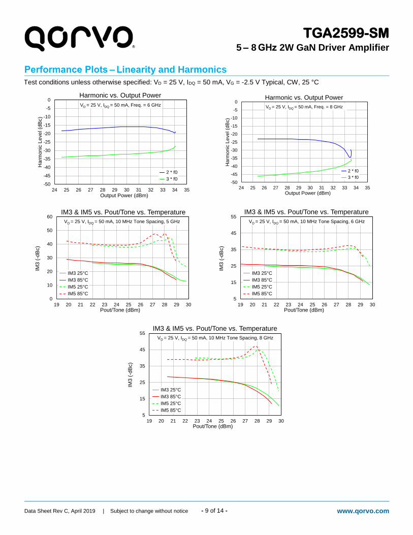
Performance Plots – Linearity and Harmonics
Test conditions unless otherwise specified: VD = 25 V, IDQ = 50 mA, VG = -2.5 V Typical, CW, 25 °C
-50
-45
-40
-35
-30
-25
-20
-15
-10
-5
0
24 25 26 27 28 29 30 31 32 33 34 35
Ha
rmo
nic
Le
ve
l (d
Bc)
Output Power (dBm)
Harmonic vs. Output Power
2 * f0
3 * f0
VD = 25 V, IDQ = 50 mA, Freq. = 6 GHz
-50
-45
-40
-35
-30
-25
-20
-15
-10
-5
0
24 25 26 27 28 29 30 31 32 33 34 35
Harm
on
ic L
eve
l (d
Bc)
Output Power (dBm)
Harmonic vs. Output Power
2 * f0
3 * f0
VD = 25 V, IDQ = 50 mA, Freq. = 8 GHz
0
10
20
30
40
50
60
19 20 21 22 23 24 25 26 27 28 29 30
IM3 (
-dB
c)
Pout/Tone (dBm)
IM3 & IM5 vs. Pout/Tone vs. Temperature
IM3 25°C
IM3 85°C
IM5 25°C
IM5 85°C
VD = 25 V, IDQ = 50 mA, 10 MHz Tone Spacing, 5 GHz
5
15
25
35
45
55
19 20 21 22 23 24 25 26 27 28 29 30
IM3 (
-dB
c)
Pout/Tone (dBm)
IM3 & IM5 vs. Pout/Tone vs. Temperature
IM3 25°C
IM3 85°C
IM5 25°C
IM5 85°C
VD = 25 V, IDQ = 50 mA, 10 MHz Tone Spacing, 6 GHz
5
15
25
35
45
55
19 20 21 22 23 24 25 26 27 28 29 30
IM3 (
-dB
c)
Pout/Tone (dBm)
IM3 & IM5 vs. Pout/Tone vs. Temperature
IM3 25°C
IM3 85°C
IM5 25°C
IM5 85°C
VD = 25 V, IDQ = 50 mA, 10 MHz Tone Spacing, 8 GHz

TGA2599-SM 5 – 8 GHz 2W GaN Driver Amplifier
Data Sheet Rev C, April 2019 | Subject to change without notice - 10 of 14 - www.qorvo.com
Application Circuit
Note: Device shown is top view, VD1 / VD2, and VG1 / VG2 can be gied together
Bias Down Procedure 1. Turn off RF signal
2. Set VG1/VG2 to -5.0V. Ensure IDQ ~ 0mA
3. Set VD1/VD2 to 0V
4. Turn off VD1/VD2 supply
5. Turn off VG1/VG2 supply
Bias Up Procedure 1. Set ID limit to 400 mA, IG limit to 4.5 mA
2. Set VG1/VG2 to -5.0V
3. Set VD1/VD2 +25V
4. Adjust VG1/VG2 more positive until IDQ = 50 mA
5. Apply RF signal

TGA2599-SM 5 – 8 GHz 2W GaN Driver Amplifier
Data Sheet Rev C, April 2019 | Subject to change without notice - 11 of 14 - www.qorvo.com
EVB and BOM
RF Layer is 0.008” thick Rogers Corp. RO4003C, r = 3.38. Metal layers are 0.5 oz. copper. The microstrip line at the
connector interface is optimized for the Southwest Microwave end launch connector 1092-01A-5. The trace pattern shown has been developed and tested for optimized assembly at Qorvo Semiconductor. The PCB land pattern has been developed to accommodate lead tolerances. Since processes vary from company to company, careful process development is recommended
Bill of Materials Reference Des. Value Description Manuf. Part Number
C3 – C6 0.01 uF Cap., 50V, 10% X7R, 0402 case Various
C1 - C2 10 uF Cap., 50V, 10% X5R, 1206 case Various
R1 – R4 0.0 Ohms Resistor, 0402 case Various
R5 – R6 5.1 Ohms Resistor, 0402 case Various

TGA2599-SM 5 – 8 GHz 2W GaN Driver Amplifier
Data Sheet Rev C, April 2019 | Subject to change without notice - 12 of 14 - www.qorvo.com
Pin Configuration and Description
Dimensions in mm. Tolerance unless otherwise stated is +/- 0.127 um.
Package lead finish: Ni / Au plating with minimum gold thickness of 0.1 um Materials: Base: Ceramic, Lid: Plastic, Part is epoxy sealed
Part Marking: 2599: Part Number, YY = Part Assembly Year, WW = Part Assembly Week, MXXX = Batch ID
Pin No. Label Description
1-2,4-5,7,9-12,14-16,18, 20 GND Connected to ground paddle (21); must be grounded to PCB to improve isolation.
3 RF Input RF input, matched to 50 Ω, DC blocked
6 VG1 First stage gate voltage. Bias network required. VG1 and VG2 can be tied together in application.
8 VG2 Second stage gate voltage. Bias network required. VG1 and VG2 can be tied together in application.
13 RF Output RF output, matched to 50 Ω, DC blocked
17 VD2 Second stage drain voltage. Bias network required. VD1 and VD2
can be tied together in application.
19 VD1 First stage drain voltage. Bias network required. VD1 and VD2
can be tied together in application.
21 GND Backside paddle. Multiple vias should be employed to minimize inductance and thermal resistance.

TGA2599-SM 5 – 8 GHz 2W GaN Driver Amplifier
Data Sheet Rev C, April 2019 | Subject to change without notice - 13 of 14 - www.qorvo.com
Solderability 1. Compatible with the latest version of J-STD-020, Lead-free solder, 260 °C.
2. The use of no-clean solder to avoid washing after soldering is recommended.
Recommended Soldering Temperature Profile

TGA2599-SM 5 – 8 GHz 2W GaN Driver Amplifier
Data Sheet Rev C, April 2019 | Subject to change without notice - 14 of 14 - www.qorvo.com
Handling Precautions Parameter Rating Standard
Caution! ESD-Sensitive Device
ESD – Human Body Model (HBM) 1A ESDA / JEDEC JS-001-2012
ESD – Charged Device Model (CDM) C3 ESDA / JEDEC JS-002-2014
MSL – Convection Reflow 260 C 3 JEDEC standard IPC/JEDEC
J-STD-020
Important Notice The information contained herein is believed to be reliable; however, Qorvo makes no warranties regarding the information contained herein and assumes no responsibility or liability whatsoever for the use of the information contained herein. All information contained herein is subject to change without notice. Customers should obtain and verify the latest relevant information before placing orders for Qorvo products. The information contained herein or any use of such information does not grant, explicitly or implicitly, to any party any patent rights, licenses, or any other intellectual property rights, whether with regard to such information itself or anything described by such information. THIS INFORMATION DOES NOT CONSTITUTE A WARRANTY WITH RESPECT TO THE PRODUCTS DESCRIBED HEREIN, AND QORVO HEREBY DISCLAIMS ANY AND ALL WARRANTIES WITH RESPECT TO SUCH PRODUCTS WHETHER EXPRESS OR IMPLIED BY LAW, COURSE OF DEALING, COURSE OF PERFORMANCE, USAGE OF TRADE OR OTHERWISE, INCLUDING THE IMPLIED WARRANTIES OF MERCHANTABILITY AND FITNESS FOR A PARTICULAR PURPOSE.
Without limiting the generality of the foregoing, Qorvo products are not warranted or authorized for use as critical components in medical, life-saving, or life-sustaining applications, or other applications where a failure would reasonably be expected to cause severe personal injury or death.
Copyright 2019 © Qorvo, Inc. | Qorvo is a registered trademark of Qorvo, Inc.
RoHS Compliance This product is compliant with the 2011/65/EU RoHS directive (Restrictions on the Use of Certain Hazardous Substances in Electrical and Electronic Equipment), as amended by Directive 2015/863/EU. This product also has the following attributes:
• Lead Free
• Halogen Free (Chlorine, Bromine)
• Antimony Free
• TBBP-A (C15H12Br402) Free
• PFOS Free
• SVHC Free
Contact Information For the latest specifications, additional product information, worldwide sales and distribution locations:
Tel: 1-844-890-8163
Web: www.qorvo.com
Email: [email protected] For technical questions and application information: Email: [email protected]