Embed Size (px)
Citation preview
LCD MODULE TFT1N5290-E Version : 1.0 May. 28, 2010
TRULY SEMICONDUCTORS LTD. TRULY CONFIDENTIAL P.1
SPECIFICATION
Revision: 1.0
TFT1N5290-E
This module uses ROHS material
TRULY SEMICONDUCTORS LTD: CUSTOMER:
PRODUCT : LCD MODULE
MODEL NO. : TFT1N5290-E
SUPPLIER : TRULY SEMICONDUCTORS LTD.
DATE : May. 28, 2010 abcdef abcdef
CERT. No. QAC0946535 CERT. No. HKG002005 (ISO9001) (ISO14001)
Quality Assurance Department: Approved by: Technical Department:
Approved by:
If there is no special request from the customer, TRULY SEMICONDUCTORS LTD. will not reserve the tooling of the product under the following conditions: 1.There is no response from the customer in two years after TRULY SEMICONDUCTORS LTD. submit the samples. 2.There is no order in two years after the latest mass production. And correlated data (including quality records) will be reserved for one year more after tooling is discarded.
LCD MODULE TFT1N5290-E Version : 1.0 May. 28, 2010
TRULY SEMICONDUCTORS LTD. TRULY CONFIDENTIAL P.2
REVISION RECORD
REV NO. REV DATE CONTENTS REMARKS
0.1 2010-5-7 First release Preliminary
1.0 2010-5-28 Full spec /
LCD MODULE TFT1N5290-E Version : 1.0 May. 28, 2010
TRULY SEMICONDUCTORS LTD. TRULY CONFIDENTIAL P.3
CONTENTS
■GENERAL INFORMATION ■EXTERNAL DIMENSIONS ■ABSOLUTE MAXIMUM RATINGS ■ELECTRICAL CHARACTERISTICS ■BACKLIGHT CHARACTERISTICS ■ELECTRO-OPTICAL CHARACTERISTICS ■INTERFACE DESCRIPTION ■REFERENCE APPLICATION CIRCUIT ■RELIABILITY TEST CONDITIONS ■INSPECTION CRITERION ■PRECAUTIONS FOR USING LCD MODULES ■PACKING SPECIFICATION ■PRIOR CONSULT MATTER ■FACTORY CONTACT INFORMATION
WRITTEN BY CHECKED BY APPROVED BY
HUANG YAN XUE YANG YAO QI KANG FEI WANG
LCD MODULE TFT1N5290-E Version : 1.0 May. 28, 2010
TRULY SEMICONDUCTORS LTD. TRULY CONFIDENTIAL P.4
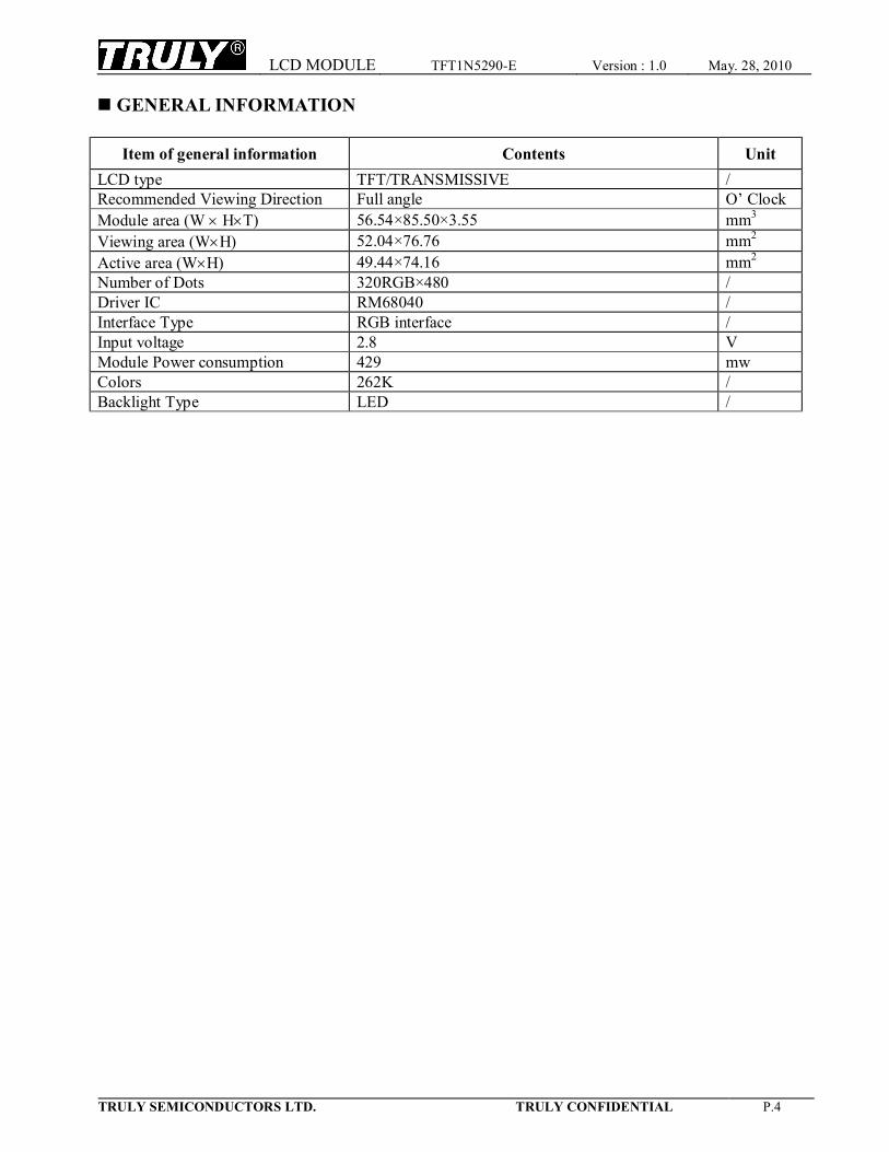
n GENERAL INFORMATION
Item of general information Contents Unit LCD type TFT/TRANSMISSIVE / Recommended Viewing Direction Full angle O’ Clock Module area (W × H×T) 56.54×85.50×3.55 mm3 Viewing area (W×H) 52.04×76.76 mm2 Active area (W×H) 49.44×74.16 mm2 Number of Dots 320RGB×480 / Driver IC RM68040 / Interface Type RGB interface / Input voltage 2.8 V Module Power consumption 429 mw Colors 262K / Backlight Type LED /
LCD MODULE TFT1N5290-E Version : 1.0 May. 28, 2010
TRULY SEMICONDUCTORS LTD. TRULY CONFIDENTIAL P.5
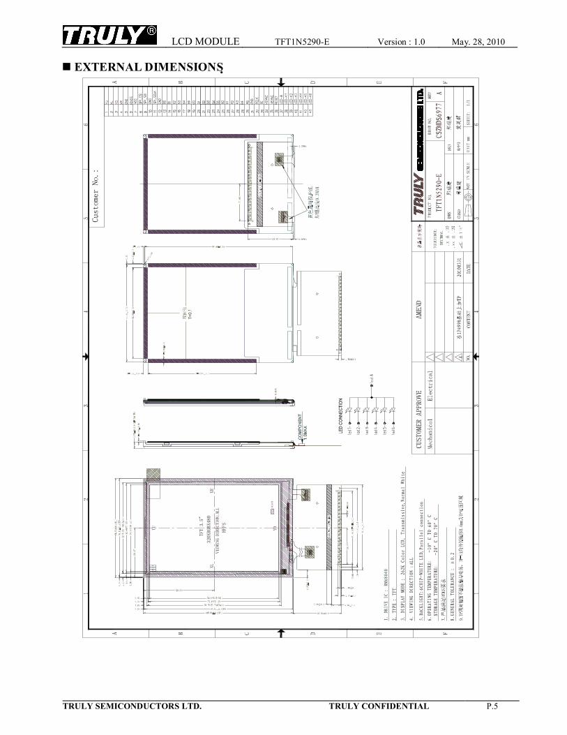
n EXTERNAL DIMENSIONS
1/1
5.BA
CKL
IGHT:
6CH
IP-
WHITE
LE
D,Par
all
el co
nne
ction
3. D
ISP
LAY M
ODE
:
262K
Col
or LC
D,
Trans
mis
sive,
Nor
mal
Whit
e
4. V
IEW
ING D
IRE
CTI
ON :A
LL
2. T
YPE
: TF
T
1. DRIVE IC : RM68040
6.O
PER
ATI
NG TE
MPE
RAT
URE:
-
10°
C TO
60°
CSTO
RAG
E TEM
PER
ATU
RE:
-
20°
C TO
70°
C
8.G
ENERA
L T
OLERA
NCE
: ±
0.2
143
143
143
VIEWING DIRECTION:ALL
HFFS
TFT 3.5"
320XRGBX480
BLACK
YD
XR
YU
XL
LCD MODULE TFT1N5290-E Version : 1.0 May. 28, 2010
TRULY SEMICONDUCTORS LTD. TRULY CONFIDENTIAL P.6
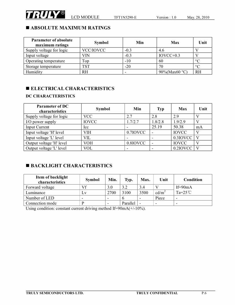
n ABSOLUTE MAXIMUM RATINGS
Parameter of absolute maximum ratings Symbol Min Max Unit
Supply voltage for logic VCC/IOVCC -0.3 4.6 V Input voltage VIN -0.3 IOVCC+0.3 V Operating temperature Top -10 60 °C Storage temperature TST -20 70 °C Humidity RH - 90%(Max60 °C) RH n ELECTRICAL CHARACTERISTICS
DC CHARACTERISTICS
Parameter of DC characteristics Symbol Min Typ Max Unit
Supply voltage for logic VCC 2.7 2.8 2.9 V I/O power supply IOVCC 1.7/2.7 1.8/2.8 1.9/2.9 V Input Current Icc - 25.19 50.38 mA Input voltage 'H' level VIH 0.7IOVCC - IOVCC V Input voltage 'L' level VIL - - 0.3IOVCC V Output voltage 'H' level VOH 0.8IOVCC - IOVCC V Output voltage 'L' level VOL - - 0.2IOVCC V n BACKLIGHT CHARACTERISTICS
Item of backlight characteristics Symbol Min. Typ. Max. Unit Condition
Forward voltage Vf 3.0 3.2 3.4 V Luminance Lv 2700 3100 3500 cd/m2
If=90mA Ta=25℃
Number of LED - - 6 - Piece - Connection mode P - Parallel - - - Using condition: constant current driving method If=90mA(+/-10%).
LCD MODULE TFT1N5290-E Version : 1.0 May. 28, 2010
TRULY SEMICONDUCTORS LTD. TRULY CONFIDENTIAL P.7
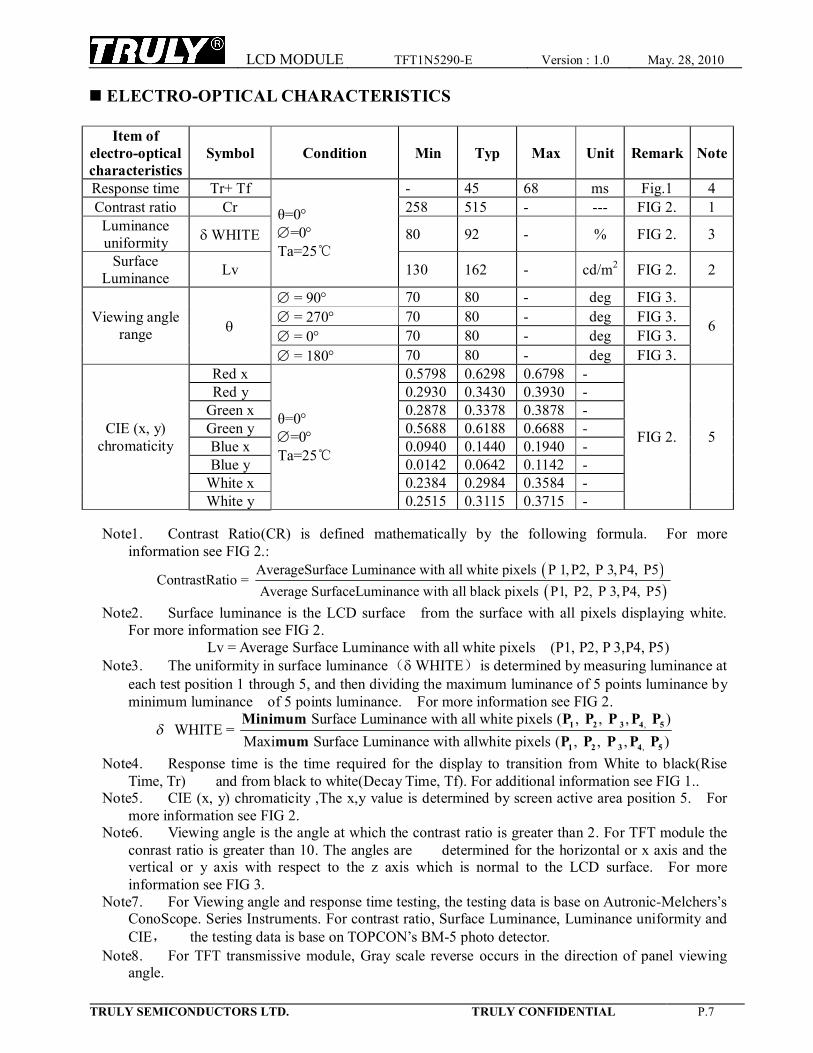
n ELECTRO-OPTICAL CHARACTERISTICS
Item of electro-optical characteristics
Symbol Condition Min Typ Max Unit Remark Note
Response time Tr+ Tf - 45 68 ms Fig.1 4 Contrast ratio Cr 258 515 - --- FIG 2. 1 Luminance uniformity δ WHITE 80 92 - % FIG 2. 3
Surface Luminance Lv
θ=0° ∅=0° Ta=25℃
130 162 - cd/m2 FIG 2. 2
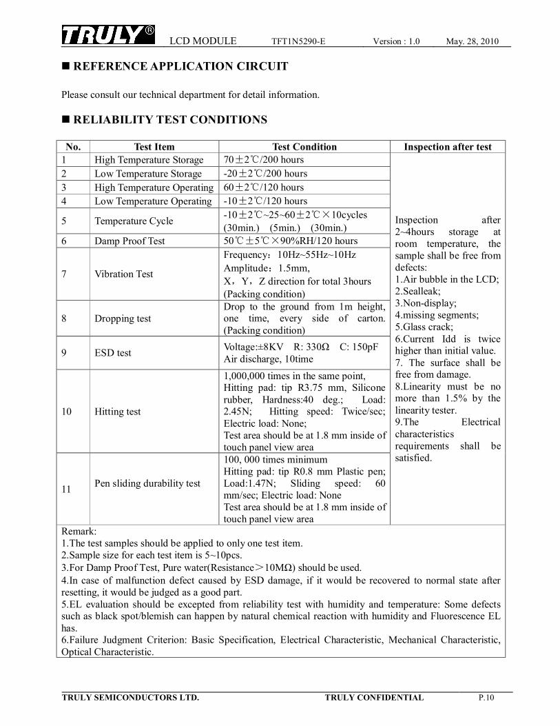
∅ = 90° 70 80 - deg FIG 3. ∅ = 270° 70 80 - deg FIG 3. ∅ = 0° 70 80 - deg FIG 3.
Viewing angle range θ
∅ = 180° 70 80 - deg FIG 3.
6
Red x 0.5798 0.6298 0.6798 - Red y 0.2930 0.3430 0.3930 -
Green x 0.2878 0.3378 0.3878 - Green y 0.5688 0.6188 0.6688 - Blue x 0.0940 0.1440 0.1940 - Blue y 0.0142 0.0642 0.1142 -
White x 0.2384 0.2984 0.3584 -
CIE (x, y) chromaticity
White y
θ=0° ∅=0° Ta=25℃
0.2515 0.3115 0.3715 -
FIG 2. 5
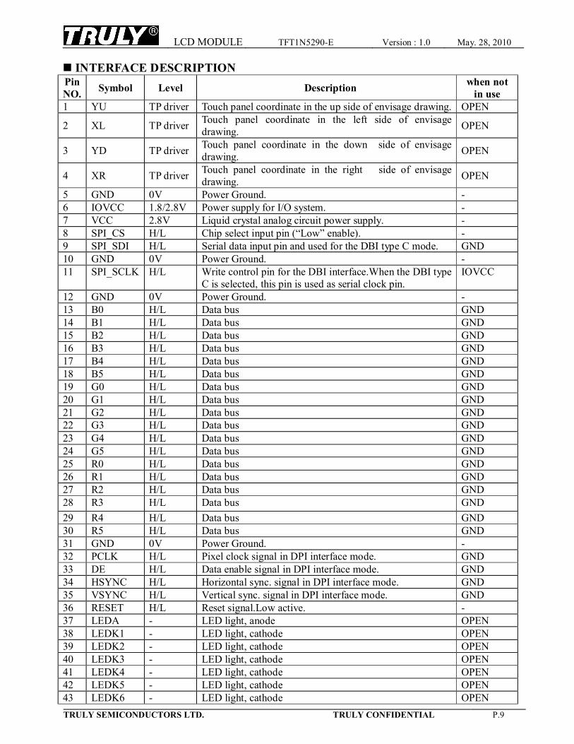
Note1. Contrast Ratio(CR) is defined mathematically by the following formula. For more
information see FIG 2.:
( )( )
AverageSurface Luminance with all white pixels P 1, P2, P 3, P4, P5 ContrastRatio =
Average SurfaceLuminance with all black pixels P1, P2, P 3, P4, P5
Note2. Surface luminance is the LCD surface from the surface with all pixels displaying white. For more information see FIG 2.
Lv = Average Surface Luminance with all white pixels (P1, P2, P 3,P4, P5) Note3. The uniformity in surface luminance (δ WHITE) is determined by measuring luminance at
each test position 1 through 5, and then dividing the maximum luminance of 5 points luminance by minimum luminance of 5 points luminance. For more information see FIG 2.
,
,
Surface Luminance with all white pixels ( , , , ) WHITE =
Maxi Surface Luminance with allwhite pixels ( , , , )δ 1 2 3 4 5
1 2 3 4 5
Minimum P P P P Pmum P P P P P
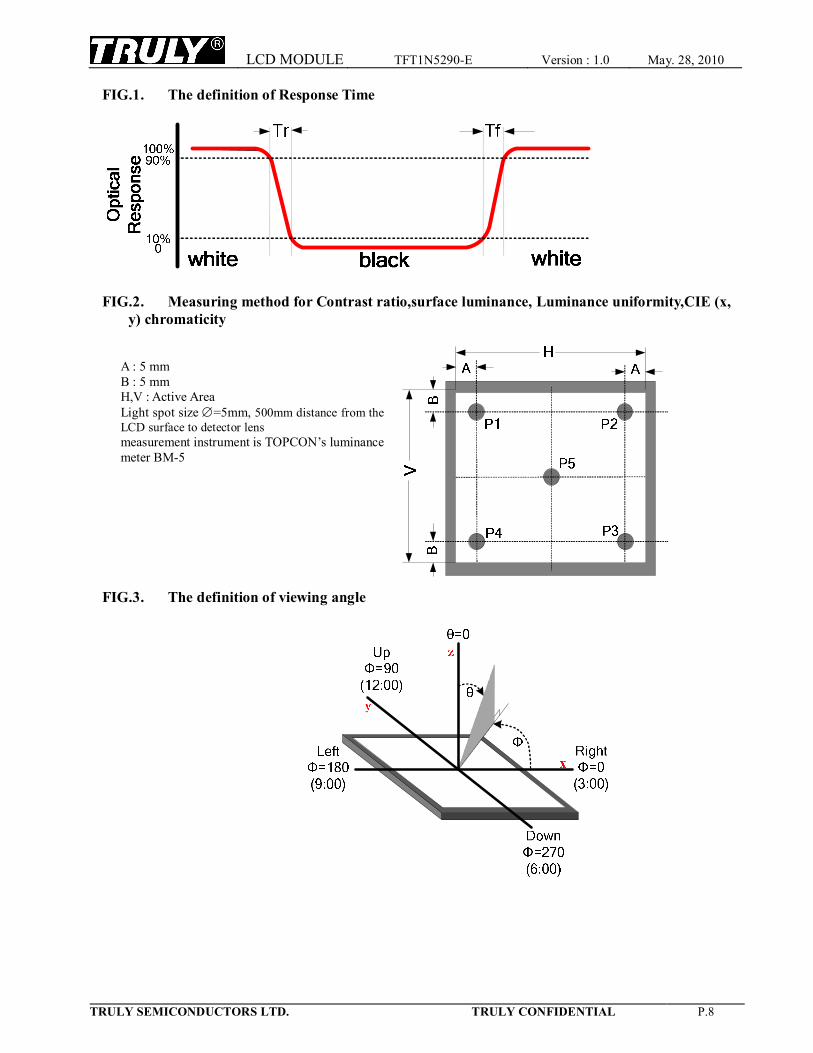
Note4. Response time is the time required for the display to transition from White to black(Rise Time, Tr) and from black to white(Decay Time, Tf). For additional information see FIG 1..
Note5. CIE (x, y) chromaticity ,The x,y value is determined by screen active area position 5. For more information see FIG 2.
Note6. Viewing angle is the angle at which the contrast ratio is greater than 2. For TFT module the conrast ratio is greater than 10. The angles are determined for the horizontal or x axis and the vertical or y axis with respect to the z axis which is normal to the LCD surface. For more information see FIG 3.
Note7. For Viewing angle and response time testing, the testing data is base on Autronic-Melchers’s ConoScope. Series Instruments. For contrast ratio, Surface Luminance, Luminance uniformity and CIE, the testing data is base on TOPCON’s BM-5 photo detector.
Note8. For TFT transmissive module, Gray scale reverse occurs in the direction of panel viewing angle.
LCD MODULE TFT1N5290-E Version : 1.0 May. 28, 2010
TRULY SEMICONDUCTORS LTD. TRULY CONFIDENTIAL P.8
FIG.1. The definition of Response Time
FIG.2. Measuring method for Contrast ratio,surface luminance, Luminance uniformity,CIE (x,
y) chromaticity
FIG.3. The definition of viewing angle
A : 5 mm B : 5 mm H,V : Active Area Light spot size ∅=5mm, 500mm distance from the LCD surface to detector lens measurement instrument is TOPCON’s luminance meter BM-5
LCD MODULE TFT1N5290-E Version : 1.0 May. 28, 2010
TRULY SEMICONDUCTORS LTD. TRULY CONFIDENTIAL P.9
n INTERFACE DESCRIPTION Pin NO. Symbol Level Description when not
in use 1 YU TP driver Touch panel coordinate in the up side of envisage drawing. OPEN
2 XL TP driver Touch panel coordinate in the left side of envisage drawing. OPEN
3 YD TP driver Touch panel coordinate in the down side of envisage drawing. OPEN
4 XR TP driver Touch panel coordinate in the right side of envisage drawing. OPEN
5 GND 0V Power Ground. - 6 IOVCC 1.8/2.8V Power supply for I/O system. - 7 VCC 2.8V Liquid crystal analog circuit power supply. - 8 SPI_CS H/L Chip select input pin (“Low” enable). - 9 SPI_SDI H/L Serial data input pin and used for the DBI type C mode. GND 10 GND 0V Power Ground. - 11 SPI_SCLK H/L Write control pin for the DBI interface.When the DBI type
C is selected, this pin is used as serial clock pin. IOVCC
12 GND 0V Power Ground. - 13 B0 H/L Data bus GND 14 B1 H/L Data bus GND 15 B2 H/L Data bus GND 16 B3 H/L Data bus GND 17 B4 H/L Data bus GND 18 B5 H/L Data bus GND 19 G0 H/L Data bus GND 20 G1 H/L Data bus GND 21 G2 H/L Data bus GND 22 G3 H/L Data bus GND 23 G4 H/L Data bus GND 24 G5 H/L Data bus GND 25 R0 H/L Data bus GND 26 R1 H/L Data bus GND 27 R2 H/L Data bus GND 28 R3 H/L Data bus GND 29 R4 H/L Data bus GND 30 R5 H/L Data bus GND 31 GND 0V Power Ground. - 32 PCLK H/L Pixel clock signal in DPI interface mode. GND 33 DE H/L Data enable signal in DPI interface mode. GND 34 HSYNC H/L Horizontal sync. signal in DPI interface mode. GND 35 VSYNC H/L Vertical sync. signal in DPI interface mode. GND 36 RESET H/L Reset signal.Low active. - 37 LEDA - LED light, anode OPEN 38 LEDK1 - LED light, cathode OPEN 39 LEDK2 - LED light, cathode OPEN 40 LEDK3 - LED light, cathode OPEN 41 LEDK4 - LED light, cathode OPEN 42 LEDK5 - LED light, cathode OPEN 43 LEDK6 - LED light, cathode OPEN
LCD MODULE TFT1N5290-E Version : 1.0 May. 28, 2010
TRULY SEMICONDUCTORS LTD. TRULY CONFIDENTIAL P.10
n REFERENCE APPLICATION CIRCUIT Please consult our technical department for detail information. n RELIABILITY TEST CONDITIONS No. Test Item Test Condition Inspection after test
1 High Temperature Storage 70±2℃/200 hours 2 Low Temperature Storage -20±2℃/200 hours 3 High Temperature Operating 60±2℃/120 hours 4 Low Temperature Operating -10±2℃/120 hours
5 Temperature Cycle -10±2℃~25~60±2℃×10cycles (30min.) (5min.) (30min.)
6 Damp Proof Test 50℃±5℃×90%RH/120 hours
7 Vibration Test
Frequency:10Hz~55Hz~10Hz Amplitude:1.5mm, X,Y,Z direction for total 3hours (Packing condition)
8 Dropping test Drop to the ground from 1m height, one time, every side of carton. (Packing condition)
9 ESD test Voltage:±8KV R: 330Ω C: 150pF Air discharge, 10time
10 Hitting test
1,000,000 times in the same point, Hitting pad: tip R3.75 mm, Silicone rubber, Hardness:40 deg.; Load: 2.45N; Hitting speed: Twice/sec; Electric load: None; Test area should be at 1.8 mm inside of touch panel view area
11 Pen sliding durability test
100, 000 times minimum Hitting pad: tip R0.8 mm Plastic pen; Load:1.47N; Sliding speed: 60 mm/sec; Electric load: None Test area should be at 1.8 mm inside of touch panel view area
Inspection after 2~4hours storage at room temperature, the sample shall be free from defects: 1.Air bubble in the LCD; 2.Sealleak; 3.Non-display; 4.missing segments; 5.Glass crack; 6.Current Idd is twice higher than initial value. 7. The surface shall be free from damage. 8.Linearity must be no more than 1.5% by the linearity tester. 9.The Electrical characteristics requirements shall be satisfied.
Remark: 1.The test samples should be applied to only one test item. 2.Sample size for each test item is 5~10pcs. 3.For Damp Proof Test, Pure water(Resistance>10MΩ) should be used. 4.In case of malfunction defect caused by ESD damage, if it would be recovered to normal state after resetting, it would be judged as a good part. 5.EL evaluation should be excepted from reliability test with humidity and temperature: Some defects such as black spot/blemish can happen by natural chemical reaction with humidity and Fluorescence EL has. 6.Failure Judgment Criterion: Basic Specification, Electrical Characteristic, Mechanical Characteristic, Optical Characteristic.
LCD MODULE TFT1N5290-E Version : 1.0 May. 28, 2010
TRULY SEMICONDUCTORS LTD. TRULY CONFIDENTIAL P.11
n INSPECTION CRITERION
This specification is made to be used as the standard acceptance/rejection criteria for Color mobile phone LCM with touch panel. 1 Sample plan Sampling plan according to GB/T2828.1-2003/ISO 2859-1:1999 and ANSI/ASQC Z1.4-1993, normal level 2 and based on: Major defect: AQL 0.65
Minor defect: AQL 1.5 2. Inspection condition
Viewing distance for cosmetic inspection is about 30cm with bare eyes, and under an environment of 20~40W light intensity, all directions for inspecting the sample should be within 45°against perpendicular line. 3. Definition of inspection zone in LCD. Zone A: character/Digit area Zone B: viewing area except Zone A (ZoneA+ZoneB=minimum Viewing area) Zone C: Outside viewing area (invisible area after assembly in customer’s product) Fig.1 Inspection zones in an LCD. Note: As a general rule, visual defects in Zone C are permissible, when it is no trouble for
quality and assembly of customer’s product.
C
B A
LCD MODULE TFT1N5290-E Version : 1.0 May. 28, 2010
TRULY SEMICONDUCTORS LTD. TRULY CONFIDENTIAL P.12
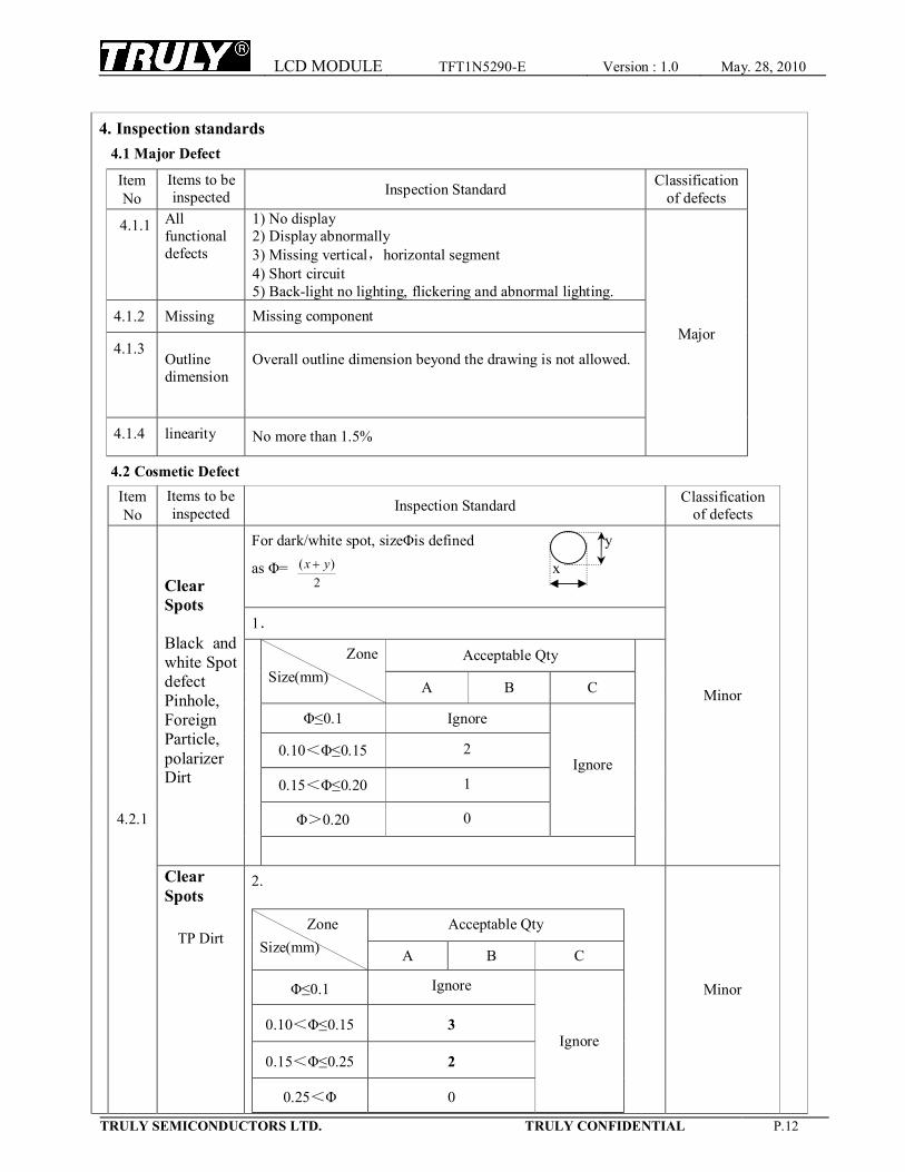
4. Inspection standards 4.1 Major Defect
Item No
Items to be inspected Inspection Standard Classification
of defects
4.1.1
All functional defects
1) No display 2) Display abnormally 3) Missing vertical,horizontal segment 4) Short circuit 5) Back-light no lighting, flickering and abnormal lighting.
4.1.2 Missing Missing component
4.1.3
Outline dimension
Overall outline dimension beyond the drawing is not allowed.
4.1.4 linearity No more than 1.5%
Major
4.2 Cosmetic Defect Item No
Items to be inspected Inspection Standard Classification
of defects
For dark/white spot, sizeΦis defined y
as Φ= 2
)( yx + x
1.
Acceptable Qty Zone Size(mm)
A B C
Φ≤0.1 Ignore
0.10<Φ≤0.15 2
0.15<Φ≤0.20 1
Φ>0.20 0
Ignore
Clear Spots Black and white Spot defect Pinhole, Foreign Particle, polarizer Dirt
Minor
4.2.1
Clear Spots
TP Dirt
2.
Acceptable Qty Zone Size(mm) A B C
Φ≤0.1 Ignore
0.10<Φ≤0.15 3
0.15<Φ≤0.25 2
0.25<Φ 0
Ignore
Minor
LCD MODULE TFT1N5290-E Version : 1.0 May. 28, 2010
TRULY SEMICONDUCTORS LTD. TRULY CONFIDENTIAL P.13
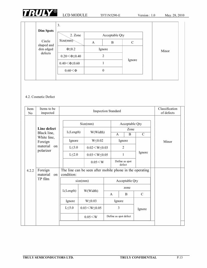
Dim Spots
Circle
shaped and dim edged
defects
3.
Acceptable Qty 2. Zone Size(mm) A B C
Φ≤0.2 Ignore
0.20<Φ≤0.40 2
0.40<Φ≤0.60 1
0.60<Φ 0
Ignore
Minor
4.2. Cosmetic Defect
Item No
Items to be inspected Inspection Standard Classification
of defects
Size(mm) Acceptable Qty Zone
L(Length) W(Width) A B C
Ignore W≤0.02 Ignore
L≤3.0 0.02<W≤0.03 2
L≤2.0 0.03<W≤0.05 1
Line defect Black line, White line, Foreign material on polarizer
0.05<W Define as spot defect
Ignore
Minor
The line can be seen after mobile phone in the operating condition:
size(mm) Acceptable Qty
zone L(Length) W(Width)
A B C
Ignore W≤0.03 Ignore
L≤5.0 0.03<W≤0.05 3
0.05<W Define as spot defect
Ignore
4.2.2 Foreign material on TP film
LCD MODULE TFT1N5290-E Version : 1.0 May. 28, 2010
TRULY SEMICONDUCTORS LTD. TRULY CONFIDENTIAL P.14
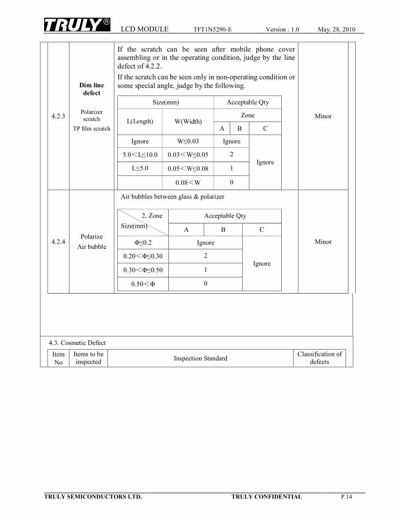
4.2.3
Dim line defect
Polarizer scratch
TP film scratch
If the scratch can be seen after mobile phone cover assembling or in the operating condition, judge by the line defect of 4.2.2. If the scratch can be seen only in non-operating condition or some special angle, judge by the following.
Size(mm) Acceptable Qty
Zone L(Length) W(Width)
A B C
Ignore W≤0.03 Ignore
5.0<L≤10.0 0.03<W≤0.05 2
L≤5.0 0.05<W≤0.08 1
0.08<W 0
Ignore
Minor
4.2.4
Polarize
Air bubble
Air bubbles between glass & polarizer
Acceptable Qty 2. Zone Size(mm) A B C
Φ≤0.2 Ignore
0.20<Φ≤0.30 2
0.30<Φ≤0.50 1
0.50<Φ 0
Ignore
Minor
4.3. Cosmetic Defect
Item No
Items to be inspected Inspection Standard Classification of
defects
LCD MODULE TFT1N5290-E Version : 1.0 May. 28, 2010
TRULY SEMICONDUCTORS LTD. TRULY CONFIDENTIAL P.15
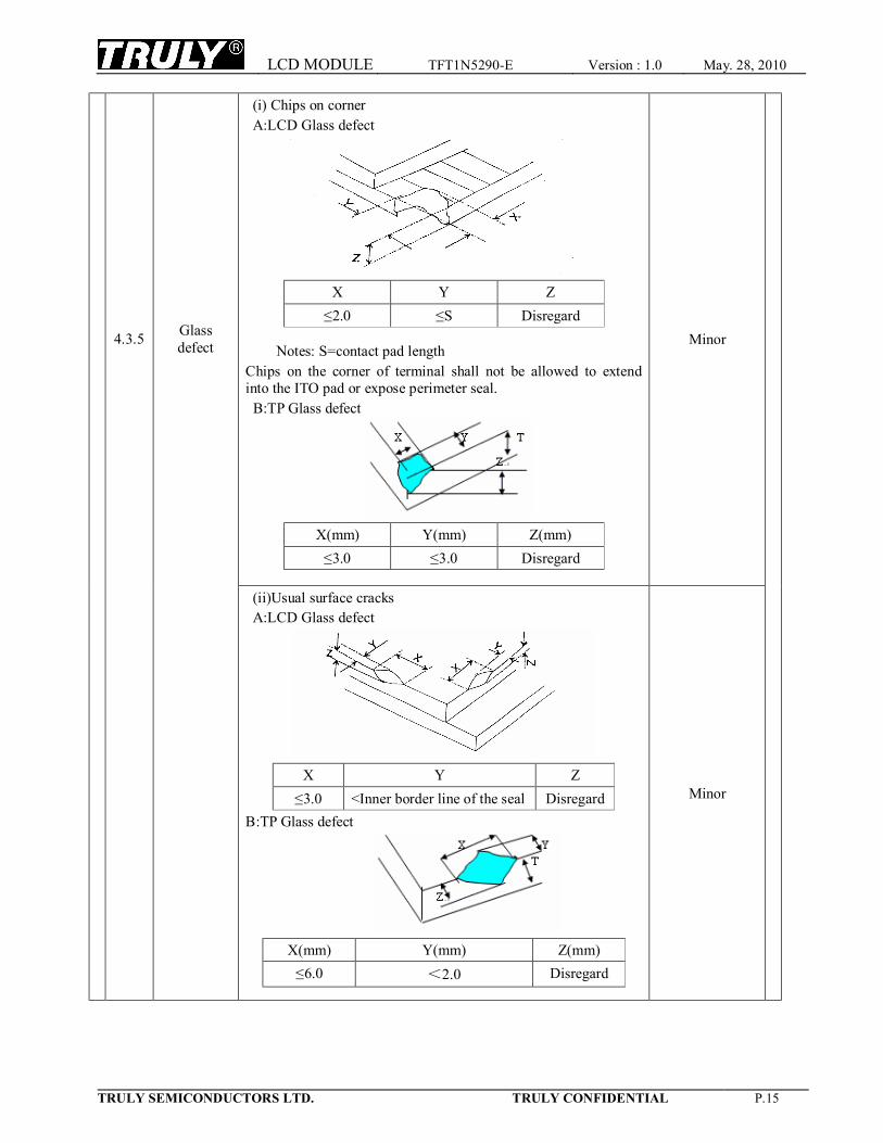
(i) Chips on corner A:LCD Glass defect
Notes: S=contact pad length Chips on the corner of terminal shall not be allowed to extend into the ITO pad or expose perimeter seal. B:TP Glass defect
X Y Z ≤2.0 ≤S Disregard
X(mm) Y(mm) Z(mm) ≤3.0 ≤3.0 Disregard
Minor 4.3.5 Glass defect
(ii)Usual surface cracks A:LCD Glass defect
B:TP Glass defect
X Y Z ≤3.0 <Inner border line of the seal Disregard
X(mm) Y(mm) Z(mm) ≤6.0 <2.0 Disregard
Minor
LCD MODULE TFT1N5290-E Version : 1.0 May. 28, 2010
TRULY SEMICONDUCTORS LTD. TRULY CONFIDENTIAL P.16
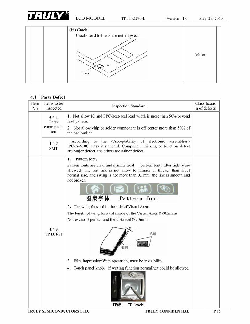
(iii) Crack Cracks tend to break are not allowed.
Major
4.4 Parts Defect
4.4.1 Parts
contraposition
1、Not allow IC and FPC/heat-seal lead width is more than 50% beyond lead pattern. 2、Not allow chip or solder component is off center more than 50% of the pad outline.
4.4.2 SMT
According to the <Acceptability of electronic assemblies> IPC-A-610C class 2 standard. Component missing or function defect are Major defect, the others are Minor defect.
4.4.3 TP Defect
1、 Pattern font: Pattern fonts are clear and symmetrical, pattern fonts filter lightly are allowed; The fort line is not allow to thinner or thicker than 1/3of normal size, and swing is not more than 0.1mm. the line is smooth and not broken.
2、The wing forward in the side of Visual Area: The length of wing forward inside of the Visual Area: n≤0.2mm; Not excess 3 point,and the distanceD≥20mm。
3、Film impression:With operation, must be invisibility.
4、Touch panel knob:if writing function normally,it could be allowed.
Item No
Items to be inspected Inspection Standard Classificatio
n of defects
LCD MODULE TFT1N5290-E Version : 1.0 May. 28, 2010
TRULY SEMICONDUCTORS LTD. TRULY CONFIDENTIAL P.17
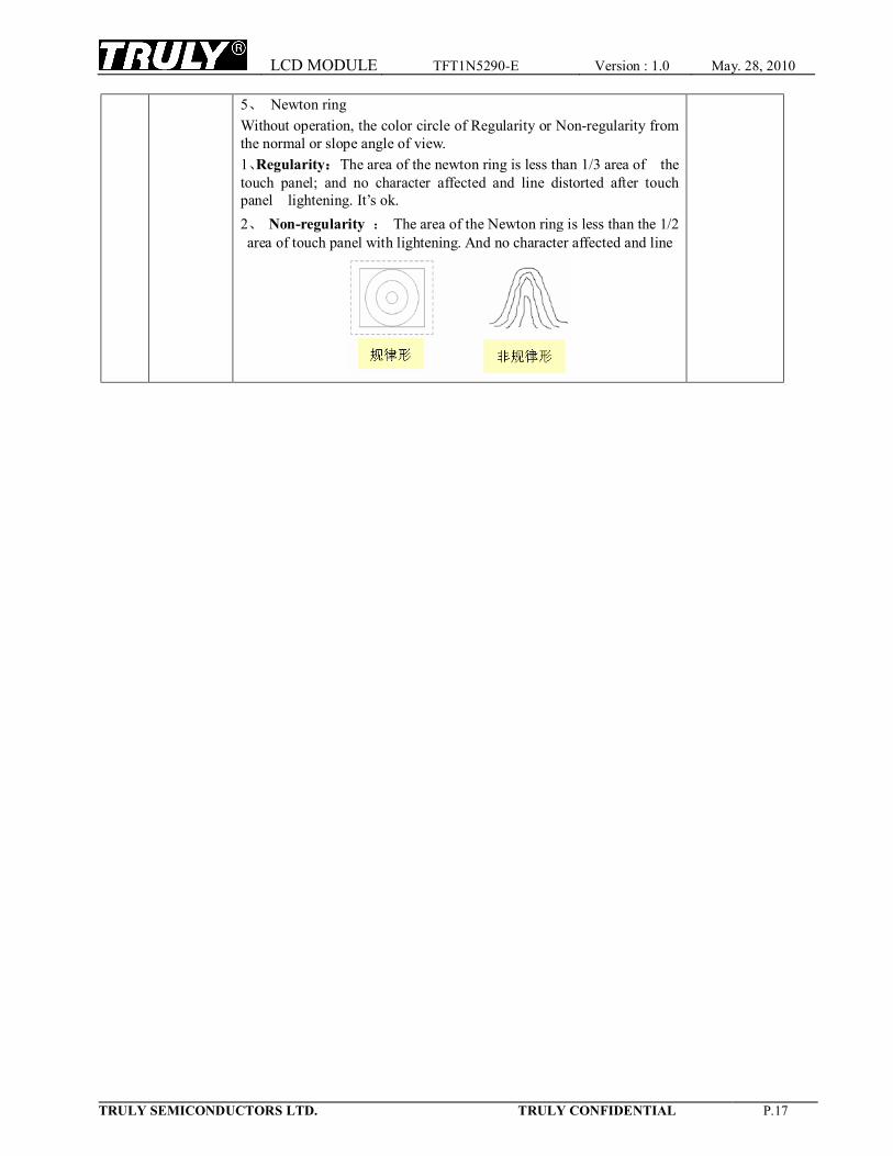
5、 Newton ring Without operation, the color circle of Regularity or Non-regularity from the normal or slope angle of view. 1、Regularity: The area of the newton ring is less than 1/3 area of the touch panel; and no character affected and line distorted after touch panel lightening. It’s ok. 2、 Non-regularity : The area of the Newton ring is less than the 1/2 area of touch panel with lightening. And no character affected and line
LCD MODULE TFT1N5290-E Version : 1.0 May. 28, 2010
TRULY SEMICONDUCTORS LTD. TRULY CONFIDENTIAL P.18
n PRECAUTIONS FOR USING LCD MODULES 1 Handing Precautions
1.1 The display panel is made of glass and polarizer. As glass is fragile. It tends to become or
chipped during handling especially on the edges. Please avoid dropping or jarring. Do not subject it to a mechanical shock by dropping it or impact.
1.2 If the display panel is damaged and the liquid crystal substance leaks out, be sure not to get any in your mouth. If the substance contacts your skin or clothes, wash it off using soap and water.
1.3 Do not apply excessive force to the display surface or the adjoining areas since this may cause the color tone to vary. Do not touch the display with bare hands. This will stain the display area and degraded insulation between terminals (some cosmetics are determined to the polarizer).
1.4 The polarizer covering the display surface of the LCD module is soft and easily scratched. Handle this polarizer carefully. Do not touch, push or rub the exposed polarizers with anything harder than an HB pencil lead (glass, tweezers, etc.). Do not put or attach anything on the display area to avoid leaving marks on it. Condensation on the surface and contact with terminals due to cold will damage, stain or dirty the polarizer. After products are tested at low temperature they must be warmed up in a container before coming in to contact with room temperature air.
1.5 If the display surface becomes contaminated, breathe on the surface and gently wipe it with a soft dry cloth. If it is heavily contaminated, moisten cloth with one of the following solvents
- Isopropyl alcohol - Ethyl alcohol Do not scrub hard to avoid damaging the display surface.
1.6 Solvents other than those above-mentioned may damage the polarizer. Especially, do not use the following.
- Water - Ketone - Aromatic solvents Wipe off saliva or water drops immediately, contact with water over a long period of time may cause deformation or color fading. Avoid contact with oil and fats.
1.7 Exercise care to minimize corrosion of the electrode. Corrosion of the electrodes is accelerated by water droplets, moisture condensation or a current flow in a high-humidity environment.
1.8 Install the LCD Module by using the mounting holes. When mounting the LCD module make sure it is free of twisting, warping and distortion. In particular, do not forcibly pull or bend the I/O cable or the backlight cable.
1.9 Do not attempt to disassemble or process the LCD module. 1.10 NC terminal should be open. Do not connect anything. 1.11 If the logic circuit power is off, do not apply the input signals. 1.12 Electro-Static Discharge Control,Since this module uses a CMOS LSI, the same careful
attention should be paid to electrostatic discharge as for an ordinary CMOS IC. To prevent destruction of the elements by static electricity, be careful to maintain an optimum work environment.
- Before removing LCM from its packing case or incorporating it into a set, be sure the module and your body have the same electric potential. Be sure to ground the body when handling the LCD modules. - Tools required for assembling, such as soldering irons, must be properly grounded. Make certain the AC power source for the soldering iron does not leak. When using an electric screwdriver to attach LCM, the screwdriver should be of ground potentiality to minimize as much as possible any transmission of electromagnetic waves produced sparks coming from the commutator of the motor. - To reduce the amount of static electricity generated, do not conduct assembling
LCD MODULE TFT1N5290-E Version : 1.0 May. 28, 2010
TRULY SEMICONDUCTORS LTD. TRULY CONFIDENTIAL P.19
and other work under dry conditions. To reduce the generation of static electricity be careful that the air in the work is not too dry. A relative humidity of 50%-60% is recommended. As far as possible make the electric potential of your work clothes and that of the work bench the ground potential. - The LCD module is coated with a film to protect the display surface. Exercise care when peeling off this protective film since static electricity may be generated.
1.13 Since LCM has been assembled and adjusted with a high degree of precision, avoid applying excessive shocks to the module or making any alterations or modifications to it.
- Do not alter, modify or change the shape of the tab on the metal frame. - Do not make extra holes on the printed circuit board, modify its shape or change the positions of components to be attached. - Do not damage or modify the pattern writing on the printed circuit board. - Absolutely do not modify the zebra rubber strip (conductive rubber) or heat seal connector. - Except for soldering the interface, do not make any alterations or modifications with a soldering iron. - Do not drop, bend or twist the LCM.
LCD MODULE TFT1N5290-E Version : 1.0 May. 28, 2010
TRULY SEMICONDUCTORS LTD. TRULY CONFIDENTIAL P.20
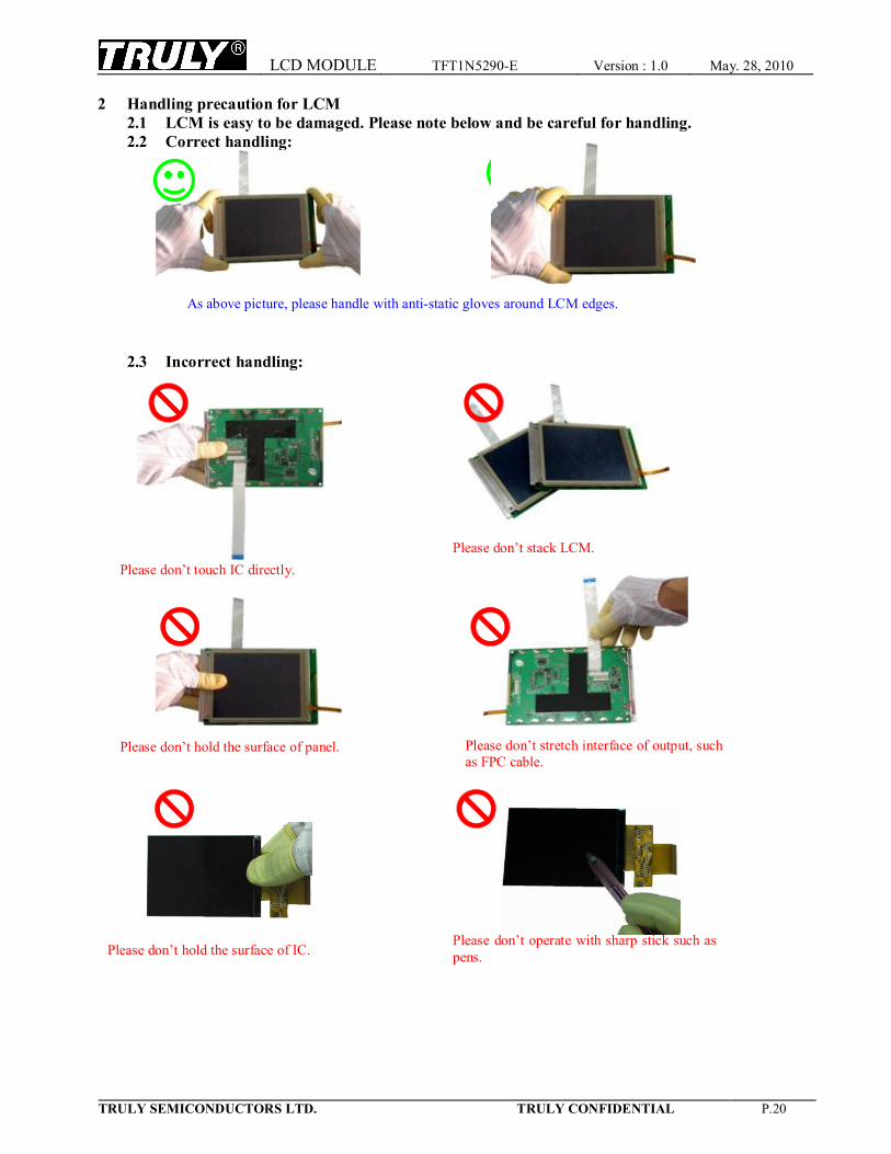
2 Handling precaution for LCM 2.1 LCM is easy to be damaged. Please note below and be careful for handling. 2.2 Correct handling:
2.3 Incorrect handling:
As above picture, please handle with anti-static gloves around LCM edges.
Please don’t hold the surface of panel.
Please don’t touch IC directly. Please don’t stack LCM.
Please don’t operate with sharp stick such as pens.
Please don’t stretch interface of output, such as FPC cable.
Please don’t hold the surface of IC.
LCD MODULE TFT1N5290-E Version : 1.0 May. 28, 2010
TRULY SEMICONDUCTORS LTD. TRULY CONFIDENTIAL P.21
3 Storage Precautions
3.1 When storing the LCD modules, the following precaution are necessary. 3.1.1 Store them in a sealed polyethylene bag. If properly sealed, there is no need for the
desiccant. 3.1.2 Store them in a dark place. Do not expose to sunlight or fluorescent light, keep the
temperature between 0°C and 35°C, and keep the relative humidity between 40%RH and 60%RH.
3.1.3 The polarizer surface should not come in contact with any other objects (We advise you to store them in the anti-static electricity container in which they were shipped).
3.2 Others 其它
3.2.1 Liquid crystals solidify under low temperature (below the storage temperature range) leading to defective orientation or the generation of air bubbles (black or white). Air bubbles may also be generated if the module is subject to a low temperature.
3.2.2 If the LCD modules have been operating for a long time showing the same display patterns, the display patterns may remain on the screen as ghost images and a slight contrast irregularity may also appear. A normal operating status can be regained by suspending use for some time. It should be noted that this phenomenon does not adversely affect performance reliability.
3.2.3 To minimize the performance degradation of the LCD modules resulting from destruction caused by static electricity etc., exercise care to avoid holding the following sections when handling the modules.
3.2.3.1 - Exposed area of the printed circuit board. 3.2.3.2 -Terminal electrode sections.
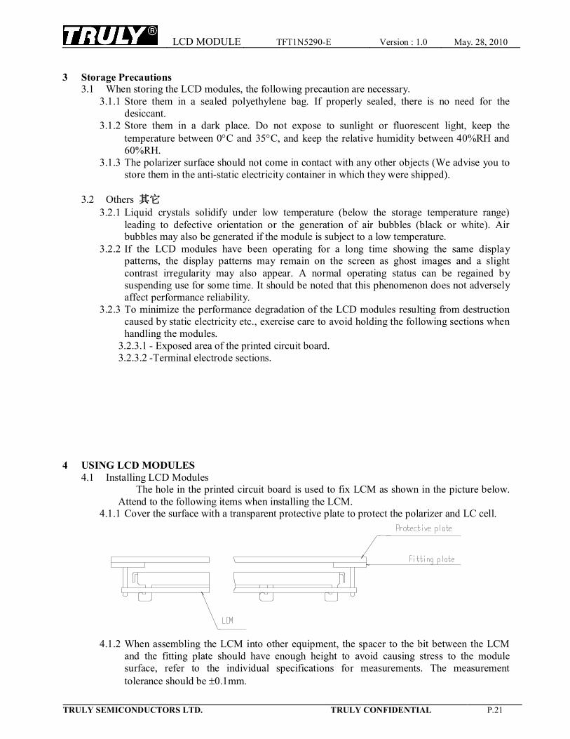
4 USING LCD MODULES 4.1 Installing LCD Modules
The hole in the printed circuit board is used to fix LCM as shown in the picture below. Attend to the following items when installing the LCM.
4.1.1 Cover the surface with a transparent protective plate to protect the polarizer and LC cell.
4.1.2 When assembling the LCM into other equipment, the spacer to the bit between the LCM
and the fitting plate should have enough height to avoid causing stress to the module surface, refer to the individual specifications for measurements. The measurement tolerance should be ±0.1mm.
LCD MODULE TFT1N5290-E Version : 1.0 May. 28, 2010
TRULY SEMICONDUCTORS LTD. TRULY CONFIDENTIAL P.22
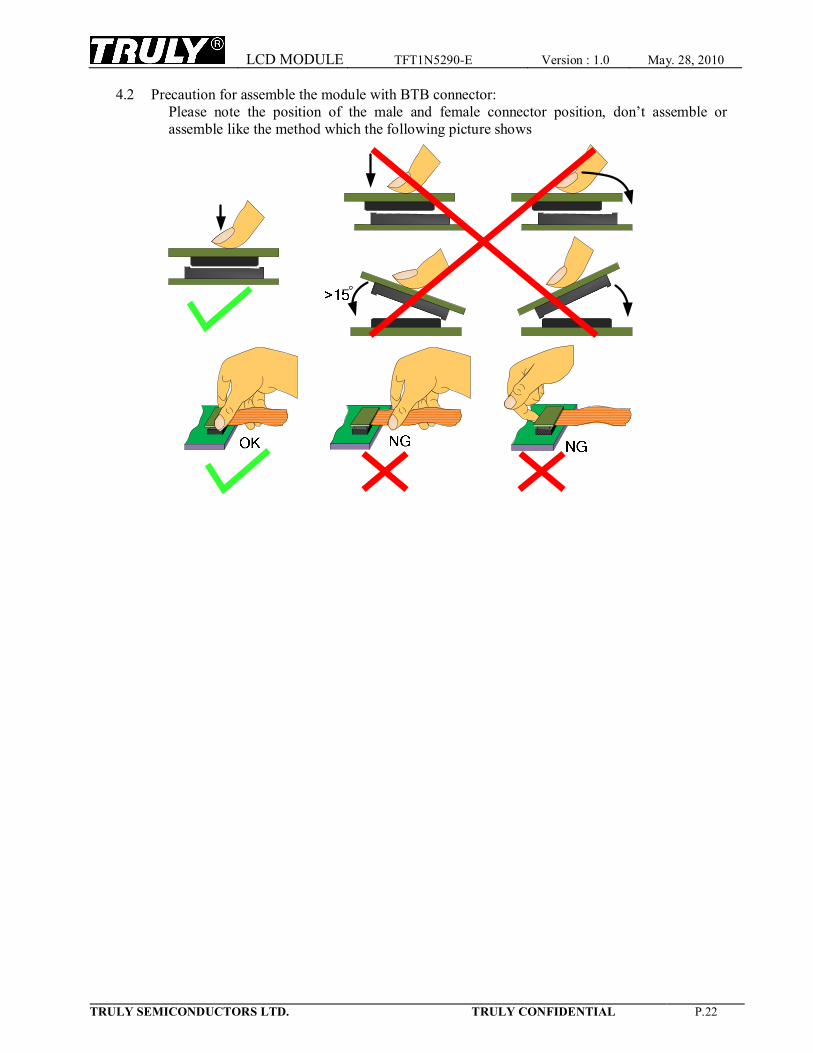
4.2 Precaution for assemble the module with BTB connector: Please note the position of the male and female connector position, don’t assemble or assemble like the method which the following picture shows
LCD MODULE TFT1N5290-E Version : 1.0 May. 28, 2010
TRULY SEMICONDUCTORS LTD. TRULY CONFIDENTIAL P.23
4.3 Precaution for soldering the LCM Manual soldering Machine drag soldering Machine press soldering
No RoHS Product
290°C ~350°C. Time : 3-5S.
330°C ~350°C. Speed : 15-17 mm/s.
300°C ~330°C. Time : 3-6S. Press: 0.8~1.2Mpa
RoHS Product
340°C ~370°C. Time : 3-5S.
350°C ~370°C. Speed : 15-17 mm/s.
330°C ~360°C. Time : 3-6S. Press: 0.8~1.2Mpa
4.3.1 If soldering flux is used, be sure to remove any remaining flux after finishing to soldering
operation (This does not apply in the case of a non-halogen type of flux). It is recommended that you protect the LCD surface with a cover during soldering to prevent any damage due to flux spatters.
4.3.2 When soldering the electroluminescent panel and PC board, the panel and board should not be detached more than three times. This maximum number is determined by the temperature and time conditions mentioned above, though there may be some variance depending on the temperature of the soldering iron.
4.3.3 When remove the electroluminescent panel from the PC board, be sure the solder has completely melted, the soldered pad on the PC board could be damaged.
4.4 Precautions for Operation 4.4.1 Viewing angle varies with the change of liquid crystal driving voltage (VLCD). Adjust
VLCD to show the best contrast. 4.4.2 It is an indispensable condition to drive LCD's within the specified voltage limit since the
higher voltage then the limit cause the shorter LCD life. An electrochemical reaction due to direct current causes LCD's undesirable deterioration, so that the use of direct current drive should be avoided.
4.4.3 Response time will be extremely delayed at lower temperature than the operating temperature range and on the other hand at higher temperature LCD's show dark color in them. However those phenomena do not mean malfunction or out of order with LCD's, which will come back in the specified operating temperature.
4.4.4 If the display area is pushed hard during operation, the display will become abnormal. However, it will return to normal if it is turned off and then back on.
4.4.5 A slight dew depositing on terminals is a cause for electro-chemical reaction resulting in terminal open circuit. Usage under the maximum operating temperature, 50%RH or less is required.
4.4.6 Input logic voltage before apply analog high voltage such as LCD driving voltage when power on. Remove analog high voltage before logic voltage when power off the module. Input each signal after the positive/negative voltage becomes stable.
4.4.7 Please keep the temperature within the specified range for use and storage. Polarization degradation, bubble generation or polarizer peel-off may occur with high temperature and high humidity.
4.5 Safety
4.5.1 It is recommended to crush damaged or unnecessary LCDs into pieces and wash them off with solvents such as acetone and ethanol, which should later be burned.
4.5.2 If any liquid leaks out of a damaged glass cell and comes in contact with the hands, wash
off thoroughly with soap and water.
LCD MODULE TFT1N5290-E Version : 1.0 May. 28, 2010
TRULY SEMICONDUCTORS LTD. TRULY CONFIDENTIAL P.24
4.6 Limited Warranty Unless agreed between TRULY and the customer, TRULY will replace or repair any of its LCD modules which are found to be functionally defective when inspected in accordance with TRULY LCD acceptance standards (copies available upon request) for a period of one year from date of production. Cosmetic/visual defects must be returned to TRULY within 90 days of shipment. Confirmation of such date shall be based on data code on product. The warranty liability of TRULY limited to repair and/or replace on the terms set forth above. TRULY will not be responsible for any subsequent or consequential events.
4.7 Return LCM under warranty
4.7.1 No warranty can be granted if the precautions stated above have been disregarded. The typical examples of violations are :
4.7.1.1 - Broken LCD glass.
4.7.1.2 - PCB eyelet is damaged or modified.
4.7.1.3 -PCB conductors damaged.
4.7.1.4 - Circuit modified in any way, including addition of components.
4.7.1.5 - PCB tampered with by grinding, engraving or painting varnish.
4.7.1.6 - Soldering to or modifying the bezel in any manner.
4.7.2 Module repairs will be invoiced to the customer upon mutual agreement. Modules must be
returned with sufficient description of the failures or defects. Any connectors or cable installed by the customer must be removed completely without damaging the PCB eyelet, conductors and terminals.
n PACKING SPECIFICATION Please consult our technical department for detail information. n PRIOR CONSULT MATTER
1 For Truly standard products, we keep the right to change material, process ... for improving the product property without prior notice to our customer.
2 For OEM products, if any changes are needed which may affect the product property, we will consult with our customer in advance.
3 If you have special requirement about reliability condition, please let us know before you start the test on our samples.
n FACTORY CONTACT INFORMATION
FACTORY NAME: TRULY SEMICONDUCTORS LTD. FACTORY ADDRESS: Truly Industrial Area, ShanWei City,GuangDong,China P.C: 516600 URL: http://www.truly.com.hk http://www.trulysemi.com