Embed Size (px)
Citation preview

The information contained in this document has been carefully researched and is, to the best of our knowledge, accurate. However, we assume no liability for any product failures or damages, immediate or consequential, resulting from the use of the information provided herein. Our products are not intended for use in systems in which failures of product could result in personal injury. All trademarks mentioned herein are property of their respective owners. All specifications are subject to change without notice.
Datasheet InnoLux G104X1-T03
CH-01-026 (Rev.C1, until Version 2.2) CH-01-026R1.1 (Rev. C2) CH-01-026R1.2 (Rev. C3) CH-01-026R1.3 (Rev. C4)
PRODUCT SPECIFICATION
Version 3.2 23 November 2018 1 / 27
The copyright belongs to InnoLux. Any unauthorized use is prohibited.
Customer: APPROVED BY SIGNATURE Name / Title Note Please return 1 copy for your confirmation with your signature and comments.
Doc. Number:
□ Tentative Specification
□ Preliminary Specification
■ Approval Specification
MODEL NO.: G104V1 SUFFIX: T03
Approved By Checked By Prepared By
許君逑許君逑許君逑許君逑
林秋森林秋森林秋森林秋森
許秝茵許秝茵許秝茵許秝茵
PRODUCT SPECIFICATION
Version 3.2 23 November 2018 2 / 27
The copyright belongs to InnoLux. Any unauthorized use is prohibited.
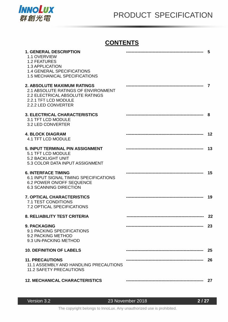
CONTENTS
1. GENERAL DESCRIPTION ------------------------------------------------------- 5 1.1 OVERVIEW 1.2 FEATURES 1.3 APPLICATION 1.4 GENERAL SPECIFICATIONS 1.5 MECHANICAL SPECIFICATIONS 2. ABSOLUTE MAXIMUM RATINGS ------------------------------------------------------- 7 2.1 ABSOLUTE RATINGS OF ENVIRONMENT 2.2 ELECTRICAL ABSOLUTE RATINGS 2.2.1 TFT LCD MODULE 2.2.2 LED CONVERTER 3. ELECTRICAL CHARACTERISTICS ------------------------------------------------------- 8 3.1 TFT LCD MODULE 3.2 LED CONVERTER
4. BLOCK DIAGRAM ------------------------------------------------------- 12 4.1 TFT LCD MODULE 5. INPUT TERMINAL PIN ASSIGNMENT ------------------------------------------------------- 13 5.1 TFT LCD MODULE 5.2 BACKLIGHT UNIT 5.3 COLOR DATA INPUT ASSIGNMENT 6. INTERFACE TIMING ------------------------------------------------------- 15 6.1 INPUT SIGNAL TIMING SPECIFICATIONS 6.2 POWER ON/OFF SEQUENCE 6.3 SCANNING DIRECTION 7. OPTICAL CHARACTERISTICS ------------------------------------------------------- 19 7.1 TEST CONDITIONS 7.2 OPTICAL SPECIFICATIONS 8. RELIABILITY TEST CRITERIA ------------------------------------------------------- 22 9. PACKAGING ------------------------------------------------------- 23 9.1 PACKING SPECIFICATIONS 9.2 PACKING METHOD 9.3 UN-PACKING METHOD 10. DEFINITION OF LABELS ------------------------------------------------------- 25 11. PRECAUTIONS ------------------------------------------------------- 26 11.1 ASSEMBLY AND HANDLING PRECAUTIONS 11.2 SAFETY PRECAUTIONS 12. MECHANICAL CHARACTERISTICS ------------------------------------------------------- 27
PRODUCT SPECIFICATION
Version 3.2 23 November 2018 3 / 27
The copyright belongs to InnoLux. Any unauthorized use is prohibited.
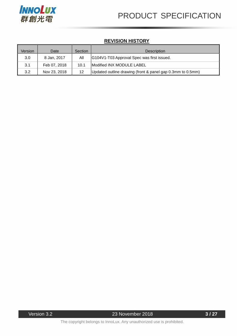
REVISION HISTORY
Version Date Section Description
3.0 8 Jan, 2017 All G104V1-T03 Approval Spec was first issued.
3.1 Feb 07, 2018 10.1 Modified INX MODULE LABEL
3.2 Nov 23, 2018 12 Updated outline drawing (front & panel gap 0.3mm to 0.5mm)
PRODUCT SPECIFICATION
Version 3.2 23 November 2018 4 / 27
The copyright belongs to InnoLux. Any unauthorized use is prohibited.
1. GENERAL DESCRIPTION
1.1 OVERVIEW
The G104V1-T03 model is a IAV 10.4” TFT-LCD module with white LED Backlight Unit and a 31-pin and 1ch
TTL interface. This module supports 640 x 480 VGA mode and display 262,144 colors. The converter for the
LED Backlight Unit is built in.
1.2 FEATURES
- Wide viewing angle
- High contrast ratio
- VGA (640 x 480 pixels) resolution
- Wide operating temperature
- DE (Data Enable) mode
- CMOS/TTL (Transistor-Transistor Logic) interface
- Reversible-scan direction
- RoHS Compliance
- LED Light Bar Replaceable
1.3 APPLICATION
- TFT LCD Monitor
- Industrial Application
- Amusement
1.4 GENERAL SPECIFICATIONS Item Specification Unit Note
Diagonal Size 10.4 inch (1) Active Area 211.2(H) x 158.4(V) mm
Bezel Opening Area 215.4(H) x 161.8(V) mm Driver Element a-si TFT active matrix - - Pixel Number 640 x R.G.B. x 480 pixel - Pixel Pitch 0.33(H) x 0.33(V) mm - Pixel Arrangement RGB vertical stripe - - Display Colors 262,144 color - Transmissive Mode Normally black - - Surface Treatment Hard coating (3H), Anti-glare (Haze 25%) - - Module Power Consumption 7.38 W Typ.
PRODUCT SPECIFICATION
Version 3.2 23 November 2018 5 / 27
The copyright belongs to InnoLux. Any unauthorized use is prohibited.
1.5 MECHANICAL SPECIFICATIONS Item Min. Typ. Max. Unit Note
Module Size Horizontal (H) 225 225.5 226 mm
(1) Vertical (V) 175.8 176.3 176.8 Mm Depth (D) 8.84(7.31) 9.34(7.81) 9.84(8.31) Mm
Weight 345 395 445 g - I/F connector mounting
position The mounting inclination of the connector makes the screen center within ±0.5mm as the horizontal.
- (2)
Note (1) Please refer to the attached drawings for more information of front and back outline dimensions. Module
depth 7.8mm does not include TTL connector, with TTL connector is 9.34mm (typical).
(2) Connector mounting position
+/- 0.5mm
PRODUCT SPECIFICATION
Version 3.2 23 November 2018 6 / 27
The copyright belongs to InnoLux. Any unauthorized use is prohibited.
2. ABSOLUTE MAXIMUM RATINGS
2.1 ABSOLUTE RATINGS OF ENVIRONMENT
Item Symbol Value
Unit Note Min. Max.
Operating Ambient Temperature TOP -30 +80 ºC (1) Storage Temperature TST -30 +80 ºC (1)
Note (1) Temperature and relative humidity range is shown in the figure below.
(a) ≦90 %RH Max. (Ta 40 ºC).
(b) Wet-bulb temperature should be 39 ºC Max. (Ta > 40 ºC).
(c) No condensation.
2.2 ELECTRICAL ABSOLUTE RATINGS
2.2.1 TFT LCD MODULE
Item Symbol Value
Unit Note Min. Max.
Power Supply Voltage VCC -0.3 7 V (1)
2.2.2 LED CONVERTER
Item Symbol Value
Unit Note Min. Max.
Converter Voltage Vi -0.3 18 V (1) , (2) Enable Voltage EN --- 5.5 V Backlight Adjust ADJ --- 5.5 V
Note (1) Permanent damage to the device may occur if maximum values are exceeded. Function operation
should be restricted to the conditions described under Normal Operating Conditions.
Note (2) Specified values are for LED (Refer to 3.2 for further information).
PRODUCT SPECIFICATION
Version 3.2 23 November 2018 7 / 27
The copyright belongs to InnoLux. Any unauthorized use is prohibited.
3. ELECTRICAL SPECIFICATIONS
3.1 TFT LCD MODULE Ta = 25 ± 2 ºC
Parameter Symbol Value
Unit Note Min. Typ. Max.
Power Supply Voltage VCC 3.0 3.3 3.6 V at VCC=3.3V
4.75 5.0 5.25 V at VCC=5.0V
Power Supply Current White
---
390 490 540 mA (3)a, at VCC=3.3V, 60Hz 290 390 440 mA (3)a, at VCC=5.0V, 60Hz
Black 370 470 520 mA (3)b, at VCC=3.3V, 60Hz 280 380 430 mA (3)b, at VCC=5.0V, 60Hz
Power Consumption PL --- 1.617 --- W VCC=3.3V, 60Hz
Logic input voltage VIH 0.7VCC - VCC V VIL 0 - 0.3VCC V
Note (1) The module is recommended to operate within specification ranges listed above for normal function.
Note (2) Measurement Conditions:
R1
(High to Low) (Control Signal)
12V
Q2
C1
1uF
Vcc
+3.3V
2SK1470
Q1 2SK1475
47K
R2
1K
VR1 47K C2
0.01uF
C3
1uF
FUSE (LCD Module Input)
Vcc rising time is 470µµµµs
470µs
+3.3V/+5V
GND
0.9Vcc
0.1Vcc
PRODUCT SPECIFICATION
Version 3.2 23 November 2018 8 / 27
The copyright belongs to InnoLux. Any unauthorized use is prohibited.
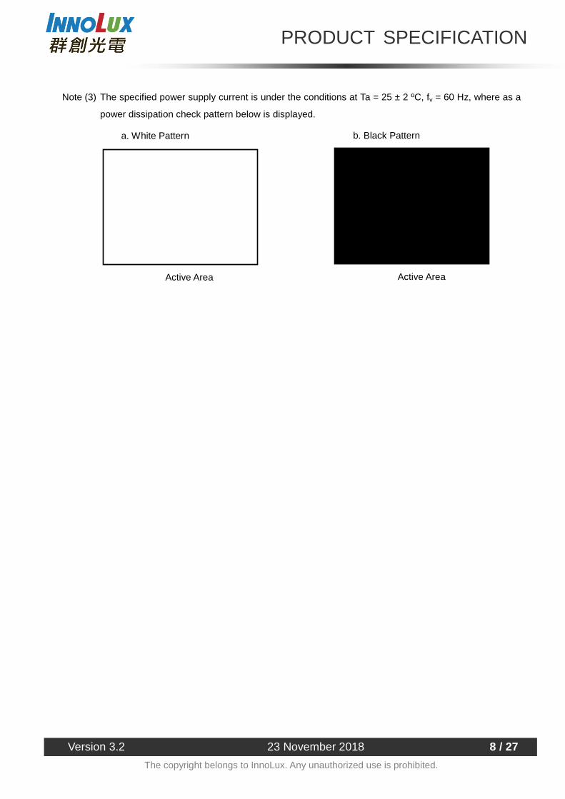
Note (3) The specified power supply current is under the conditions at Ta = 25 ± 2 ºC, fv = 60 Hz, where as a
power dissipation check pattern below is displayed.
Active Area
a. White Pattern
Active Area
b. Black Pattern
PRODUCT SPECIFICATION
Version 3.2 23 November 2018 9 / 27
The copyright belongs to InnoLux. Any unauthorized use is prohibited.
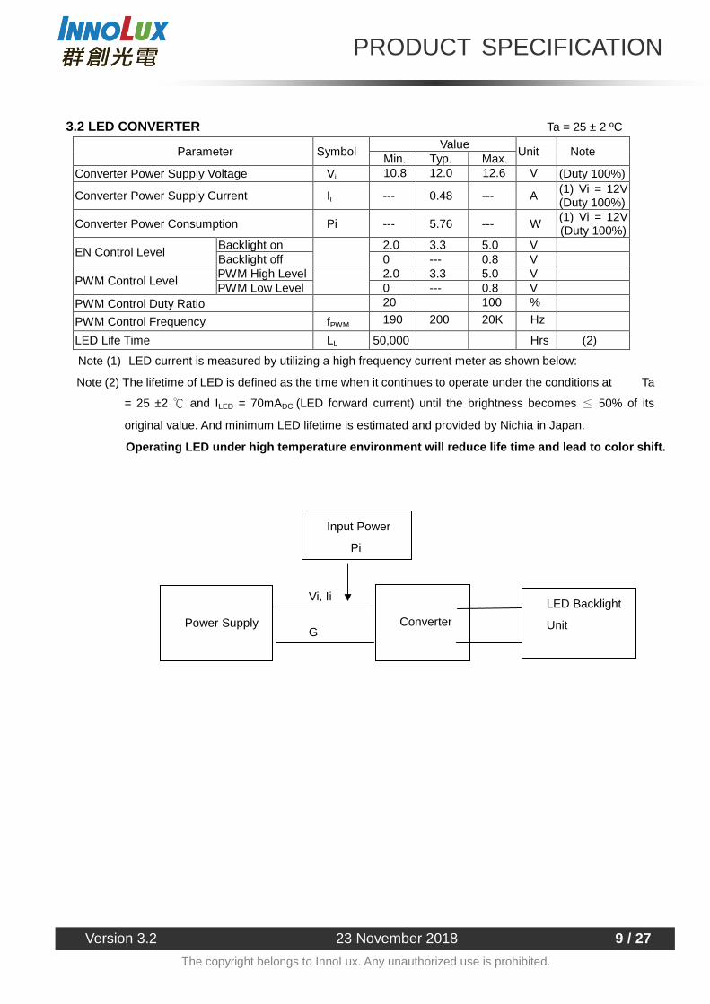
3.2 LED CONVERTER Ta = 25 ± 2 ºC
Parameter Symbol Value
Unit Note Min. Typ. Max.
Converter Power Supply Voltage Vi 10.8 12.0 12.6 V (Duty 100%)
Converter Power Supply Current Ii --- 0.48 --- A (1) Vi = 12V (Duty 100%)
Converter Power Consumption Pi --- 5.76 --- W (1) Vi = 12V (Duty 100%)
EN Control Level Backlight on
2.0 3.3 5.0 V
Backlight off 0 --- 0.8 V
PWM Control Level PWM High Level
2.0 3.3 5.0 V
PWM Low Level 0 --- 0.8 V PWM Control Duty Ratio 20 100 %
PWM Control Frequency fPWM 190 200 20K Hz
LED Life Time LL 50,000 Hrs (2)
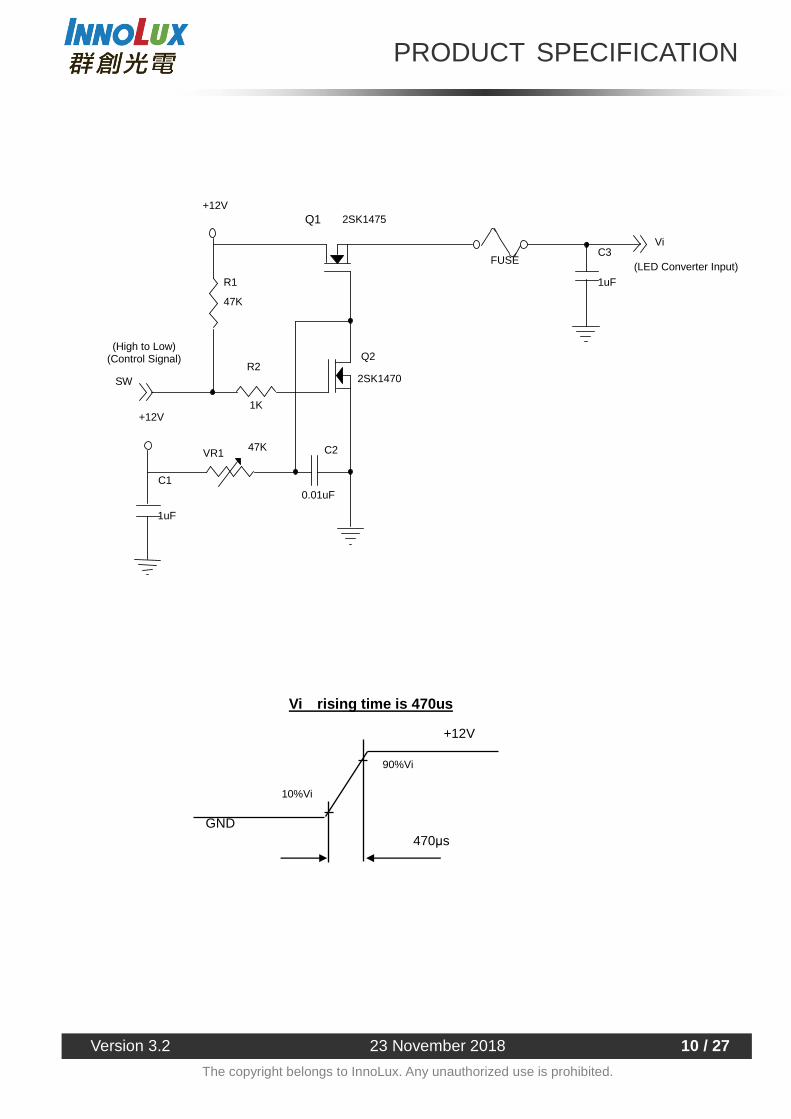
Note (1) LED current is measured by utilizing a high frequency current meter as shown below:
Note (2) The lifetime of LED is defined as the time when it continues to operate under the conditions at Ta
= 25 ±2 ℃ and ILED = 70mADC ≦(LED forward current) until the brightness becomes 50% of its
original value. And minimum LED lifetime is estimated and provided by Nichia in Japan.
Operating LED under high temperature environment will reduce life time and lead to color shift.
Power Supply
Converter
LED Backlight
Unit
Vi, Ii
G
Input Power
Pi
PRODUCT SPECIFICATION
Version 3.2 23 November 2018 10 / 27
The copyright belongs to InnoLux. Any unauthorized use is prohibited.
R1
(High to Low) (Control Signal)
+12V
SW
Q2
C1
1uF
Vi
+12V
2SK1470
Q1 2SK1475
47K
R2
1K
VR1 47K C2
0.01uF
C3
1uF
FUSE (LED Converter Input)
Vi rising time is 470us
470µs
+12V
GND
90%Vi
10%Vi
PRODUCT SPECIFICATION
Version 3.2 23 November 2018 11 / 27
The copyright belongs to InnoLux. Any unauthorized use is prohibited.
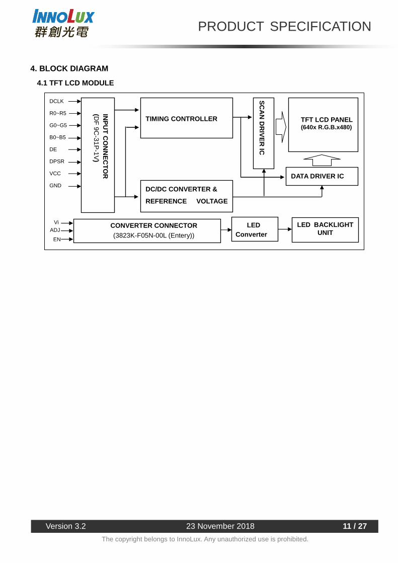
4. BLOCK DIAGRAM
4.1 TFT LCD MODULE
TFT LCD PANEL (640x R.G.B.x480)
DATA DRIVER IC
SC
AN
DR
IVE
R IC
TIMING CONTROLLER
DC/DC CONVERTER &
REFERENCE VOLTAGE
Vi
INP
UT
CO
NN
EC
TOR
(D
F 9C
-31P-1V
)
LED Converter
LED BACKLIGHT UNIT
CONVERTER CONNECTOR
(3823K-F05N-00L (Entery)) ADJ
EN
DCLK
R0~R5
G0~G5
B0~B5
DE
DPSR
VCC
GND
PRODUCT SPECIFICATION
Version 3.2 23 November 2018 12 / 27
The copyright belongs to InnoLux. Any unauthorized use is prohibited.
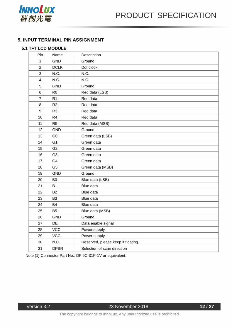
5. INPUT TERMINAL PIN ASSIGNMENT
5.1 TFT LCD MODULE
Pin Name Description
1 GND Ground
2 DCLK Dot clock
3 N.C. N.C.
4 N.C. N.C.
5 GND Ground
6 R0 Red data (LSB)
7 R1 Red data
8 R2 Red data
9 R3 Red data
10 R4 Red data
11 R5 Red data (MSB)
12 GND Ground
13 G0 Green data (LSB)
14 G1 Green data
15 G2 Green data
16 G3 Green data
17 G4 Green data
18 G5 Green data (MSB)
19 GND Ground
20 B0 Blue data (LSB)
21 B1 Blue data
22 B2 Blue data
23 B3 Blue data
24 B4 Blue data
25 B5 Blue data (MSB)
26 GND Ground
27 DE Data enable signal
28 VCC Power supply
29 VCC Power supply
30 N.C. Reserved, please keep it floating.
31 DPSR Selection of scan direction
Note (1) Connector Part No.: DF 9C-31P-1V or equivalent.
PRODUCT SPECIFICATION
Version 3.2 23 November 2018 13 / 27
The copyright belongs to InnoLux. Any unauthorized use is prohibited.
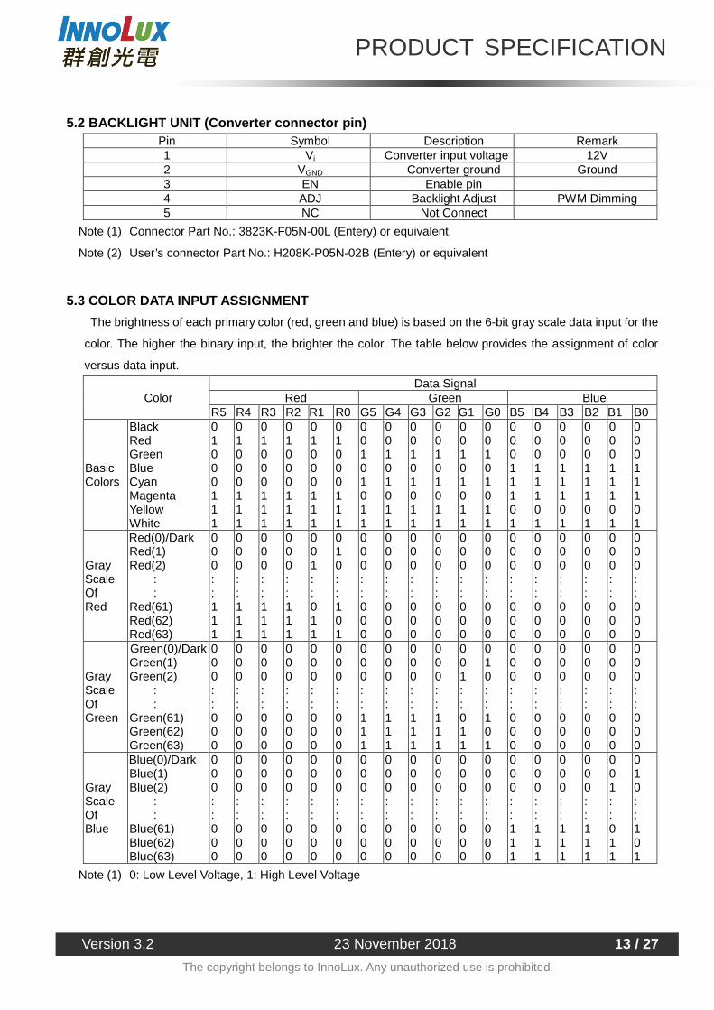
5.2 BACKLIGHT UNIT (Converter connector pin) Pin Symbol Description Remark 1 Vi Converter input voltage 12V 2 VGND Converter ground Ground 3 EN Enable pin 4 ADJ Backlight Adjust PWM Dimming 5 NC Not Connect
Note (1) Connector Part No.: 3823K-F05N-00L (Entery) or equivalent
Note (2) User’s connector Part No.: H208K-P05N-02B (Entery) or equivalent
5.3 COLOR DATA INPUT ASSIGNMENT
The brightness of each primary color (red, green and blue) is based on the 6-bit gray scale data input for the
color. The higher the binary input, the brighter the color. The table below provides the assignment of color
versus data input.
Color Data Signal
Red Green Blue R5 R4 R3 R2 R1 R0 G5 G4 G3 G2 G1 G0 B5 B4 B3 B2 B1 B0
Basic Colors
Black Red Green Blue Cyan Magenta Yellow White
0 1 0 0 0 1 1 1
0 1 0 0 0 1 1 1
0 1 0 0 0 1 1 1
0 1 0 0 0 1 1 1
0 1 0 0 0 1 1 1
0 1 0 0 0 1 1 1
0 0 1 0 1 0 1 1
0 0 1 0 1 0 1 1
0 0 1 0 1 0 1 1
0 0 1 0 1 0 1 1
0 0 1 0 1 0 1 1
0 0 1 0 1 0 1 1
0 0 0 1 1 1 0 1
0 0 0 1 1 1 0 1
0 0 0 1 1 1 0 1
0 0 0 1 1 1 0 1
0 0 0 1 1 1 0 1
0 0 0 1 1 1 0 1
Gray Scale Of Red
Red(0)/Dark Red(1) Red(2)
: :
Red(61) Red(62) Red(63)
0 0 0 : : 1 1 1
0 0 0 : : 1 1 1
0 0 0 : : 1 1 1
0 0 0 : : 1 1 1
0 0 1 : : 0 1 1
0 1 0 : : 1 0 1
0 0 0 : : 0 0 0
0 0 0 : : 0 0 0
0 0 0 : : 0 0 0
0 0 0 : : 0 0 0
0 0 0 : : 0 0 0
0 0 0 : : 0 0 0
0 0 0 : : 0 0 0
0 0 0 : : 0 0 0
0 0 0 : : 0 0 0
0 0 0 : : 0 0 0
0 0 0 : : 0 0 0
0 0 0 : : 0 0 0
Gray Scale Of Green
Green(0)/Dark Green(1) Green(2)
: :
Green(61) Green(62) Green(63)
0 0 0 : : 0 0 0
0 0 0 : : 0 0 0
0 0 0 : : 0 0 0
0 0 0 : : 0 0 0
0 0 0 : : 0 0 0
0 0 0 : : 0 0 0
0 0 0 : : 1 1 1
0 0 0 : : 1 1 1
0 0 0 : : 1 1 1
0 0 0 : : 1 1 1
0 0 1 : : 0 1 1
0 1 0 : : 1 0 1
0 0 0 : : 0 0 0
0 0 0 : : 0 0 0
0 0 0 : : 0 0 0
0 0 0 : : 0 0 0
0 0 0 : : 0 0 0
0 0 0 : : 0 0 0
Gray Scale Of Blue
Blue(0)/Dark Blue(1) Blue(2)
: :
Blue(61) Blue(62) Blue(63)
0 0 0 : : 0 0 0
0 0 0 : : 0 0 0
0 0 0 : : 0 0 0
0 0 0 : : 0 0 0
0 0 0 : : 0 0 0
0 0 0 : : 0 0 0
0 0 0 : : 0 0 0
0 0 0 : : 0 0 0
0 0 0 : : 0 0 0
0 0 0 : : 0 0 0
0 0 0 : : 0 0 0
0 0 0 : : 0 0 0
0 0 0 : : 1 1 1
0 0 0 : : 1 1 1
0 0 0 : : 1 1 1
0 0 0 : : 1 1 1
0 0 1 : : 0 1 1
0 1 0 : : 1 0 1
Note (1) 0: Low Level Voltage, 1: High Level Voltage
PRODUCT SPECIFICATION
Version 3.2 23 November 2018 14 / 27
The copyright belongs to InnoLux. Any unauthorized use is prohibited.
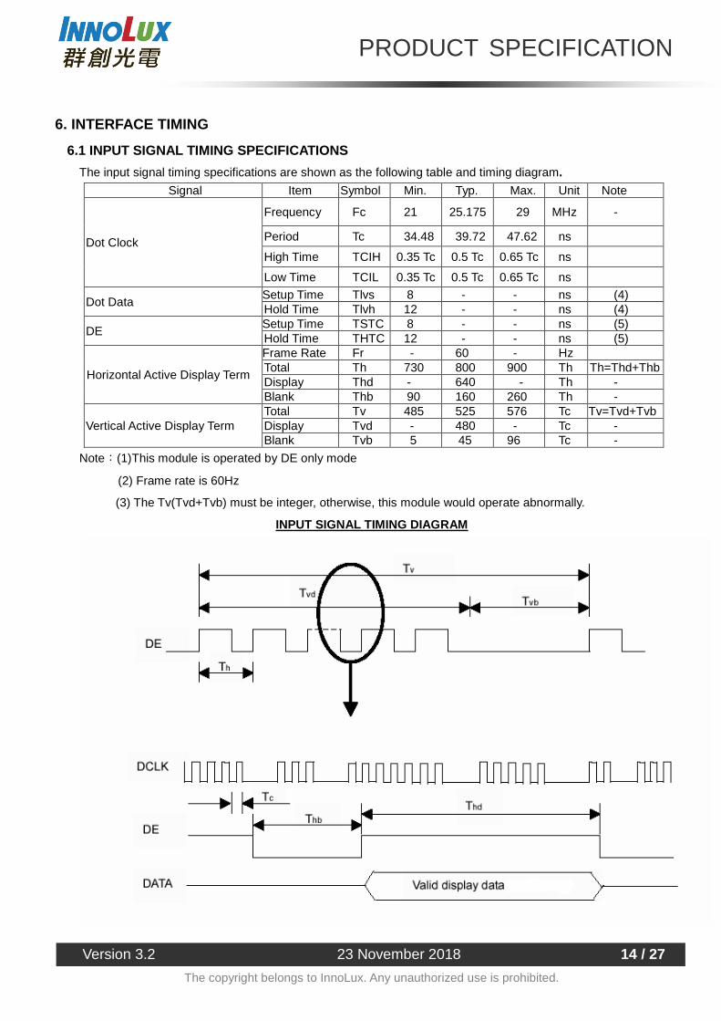
6. INTERFACE TIMING
6.1 INPUT SIGNAL TIMING SPECIFICATIONS
The input signal timing specifications are shown as the following table and timing diagram.
Signal Item Symbol Min. Typ. Max. Unit Note
Dot Clock
Frequency Fc 21 25.175 29 MHz -
Period Tc 34.48 39.72 47.62 ns
High Time TCIH 0.35 Tc 0.5 Tc 0.65 Tc ns
Low Time TCIL 0.35 Tc 0.5 Tc 0.65 Tc ns
Dot Data Setup Time Tlvs 8 - - ns (4) Hold Time Tlvh 12 - - ns (4)
DE Setup Time TSTC 8 - - ns (5) Hold Time THTC 12 - - ns (5)
Horizontal Active Display Term
Frame Rate Fr - 60 - Hz Total Th 730 800 900 Th Th=Thd+Thb Display Thd - 640 - Th - Blank Thb 90 160 260 Th -
Vertical Active Display Term Total Tv 485 525 576 Tc Tv=Tvd+Tvb Display Tvd - 480 - Tc - Blank Tvb 5 45 96 Tc -
Note:(1)This module is operated by DE only mode
(2) Frame rate is 60Hz
(3) The Tv(Tvd+Tvb) must be integer, otherwise, this module would operate abnormally.
INPUT SIGNAL TIMING DIAGRAM
PRODUCT SPECIFICATION
Version 3.2 23 November 2018 15 / 27
The copyright belongs to InnoLux. Any unauthorized use is prohibited.
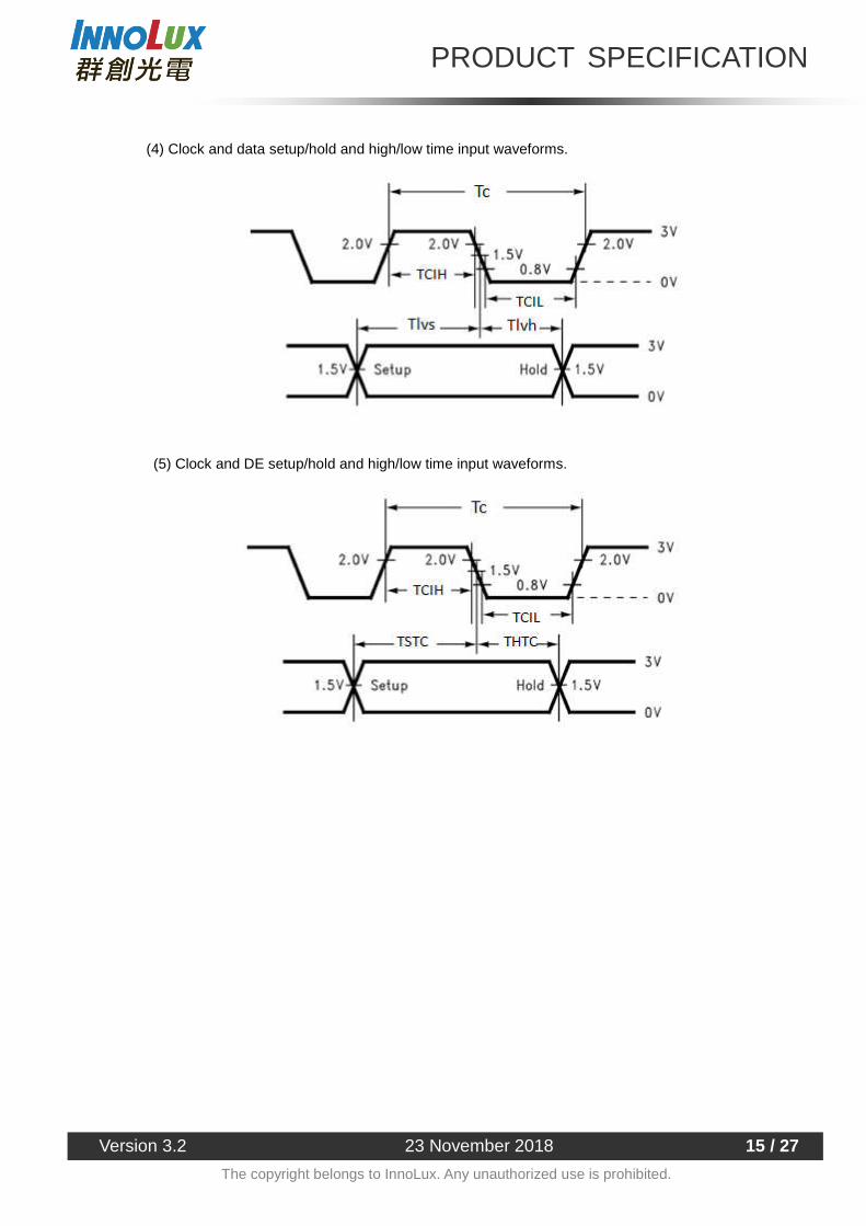
(4) Clock and data setup/hold and high/low time input waveforms.
(5) Clock and DE setup/hold and high/low time input waveforms.
PRODUCT SPECIFICATION
Version 3.2 23 November 2018 16 / 27
The copyright belongs to InnoLux. Any unauthorized use is prohibited.
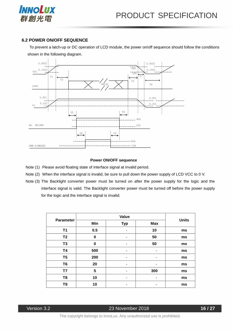
6.2 POWER ON/OFF SEQUENCE
To prevent a latch-up or DC operation of LCD module, the power on/off sequence should follow the conditions
shown in the following diagram.
Power ON/OFF sequence
Note (1) Please avoid floating state of interface signal at invalid period.
Note (2) When the interface signal is invalid, be sure to pull down the power supply of LCD VCC to 0 V.
Note (3) The Backlight converter power must be turned on after the power supply for the logic and the
interface signal is valid. The Backlight converter power must be turned off before the power supply
for the logic and the interface signal is invalid.
Parameter Value
Units Min Typ Max
T1 0.5 - 10 ms
T2 0 - 50 ms
T3 0 - 50 ms
T4 500 - - ms
T5 200 - - ms
T6 20 - - ms
T7 5 - 300 ms
T8 10 - - ms
T9 10 - - ms
LVDS
VCC
Vi
10%
90%
T2T1
T3
0.1VCC
0.9VCC 0.9VCC
0.1VCC
T4VALID
T7
0.9Vi 0.9Vi
0.1Vi 0.1Vi
PWM DIMMING
T9
10%
90%
T8
BL ON/OFF
T5
10%
90%
T6
Version 3.2
The copyright belongs to InnoLux. Any unauthorized use is prohibited.
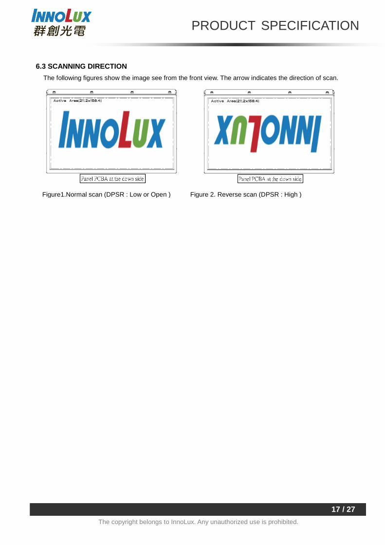
6.3 SCANNING DIRECTION
The following figures show the image see from the front view. The arrow indicates the direction of scan.
Figure1.Normal scan (DPSR : Low or Open ) Figure 2. Reverse scan (DPSR : High )
PRODUCT SPECIFICATION
23 November 2018
The copyright belongs to InnoLux. Any unauthorized use is prohibited.
SCANNING DIRECTION
The following figures show the image see from the front view. The arrow indicates the direction of scan.
Figure1.Normal scan (DPSR : Low or Open ) Figure 2. Reverse scan (DPSR : High )
PRODUCT SPECIFICATION
17 / 27
The copyright belongs to InnoLux. Any unauthorized use is prohibited.
The following figures show the image see from the front view. The arrow indicates the direction of scan.
Figure1.Normal scan (DPSR : Low or Open ) Figure 2. Reverse scan (DPSR : High )
PRODUCT SPECIFICATION
Version 3.2 23 November 2018 18 / 27
The copyright belongs to InnoLux. Any unauthorized use is prohibited.
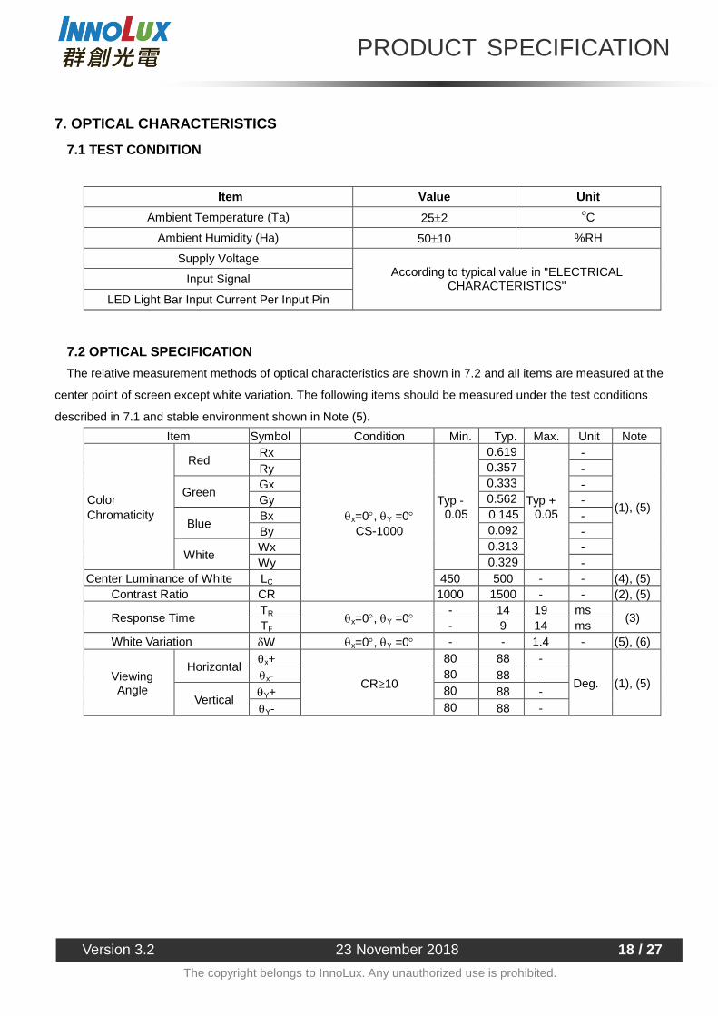
7. OPTICAL CHARACTERISTICS
7.1 TEST CONDITION
Item Value Unit
Ambient Temperature (Ta) 25±2 oC
Ambient Humidity (Ha) 50±10 %RH
Supply Voltage According to typical value in "ELECTRICAL
CHARACTERISTICS" Input Signal
LED Light Bar Input Current Per Input Pin
7.2 OPTICAL SPECIFICATION
The relative measurement methods of optical characteristics are shown in 7.2 and all items are measured at the
center point of screen except white variation. The following items should be measured under the test conditions
described in 7.1 and stable environment shown in Note (5).
Item Symbol Condition Min. Typ. Max. Unit Note
Color Chromaticity
Red Rx
θx=0°, θY =0° CS-1000
Typ - 0.05
0.619
Typ + 0.05
-
(1), (5)
Ry 0.357 -
Green Gx 0.333 - Gy 0.562 -
Blue Bx 0.145 - By 0.092 -
White Wx 0.313 - Wy 0.329 -
Center Luminance of White LC 450 500 - - (4), (5) Contrast Ratio CR 1000 1500 - - (2), (5)
Response Time TR
θx=0°, θY =0° - 14 19 ms
(3) TF - 9 14 ms
White Variation δW θx=0°, θY =0° - - 1.4 - (5), (6)
Viewing Angle
Horizontal θx+
CR≥10
80 88 -
Deg. (1), (5) θx- 80 88 -
Vertical θY+ 80 88 - θY- 80 88 -
PRODUCT SPECIFICATION
Version 3.2 23 November 2018 19 / 27
The copyright belongs to InnoLux. Any unauthorized use is prohibited.
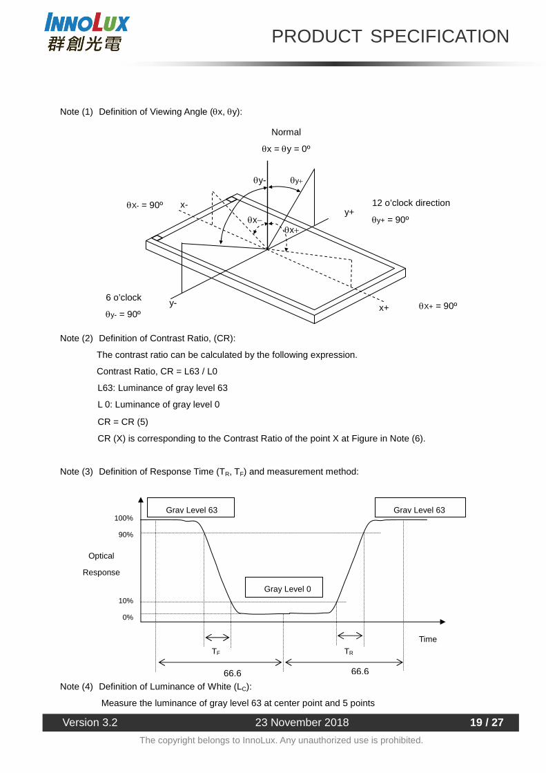
Note (1) Definition of Viewing Angle (θx, θy):
Note (2) Definition of Contrast Ratio, (CR):
The contrast ratio can be calculated by the following expression.
Contrast Ratio, CR = L63 / L0
L63: Luminance of gray level 63
L 0: Luminance of gray level 0
CR = CR (5)
CR (X) is corresponding to the Contrast Ratio of the point X at Figure in Note (6).
Note (3) Definition of Response Time (TR, TF) and measurement method:
Note (4) Definition of Luminance of White (LC):
Measure the luminance of gray level 63 at center point and 5 points
100%
90%
10%
0%
Gray Level 63
Gray Level 0
Gray Level 63
Time
TR
Optical
Response
TF
66.6 66.6
12 o’clock direction
θy+ = 90º
6 o’clock
θy- = 90º
θx− θx+
θy- θy+
x- y+
y- x+
Normal
θx = θy = 0º
θX+ = 90º
θX- = 90º
PRODUCT SPECIFICATION
Version 3.2 23 November 2018 20 / 27
The copyright belongs to InnoLux. Any unauthorized use is prohibited.
LC = L (5), where L (X) is corresponding to the luminance of the point X at the figure in Note (6).
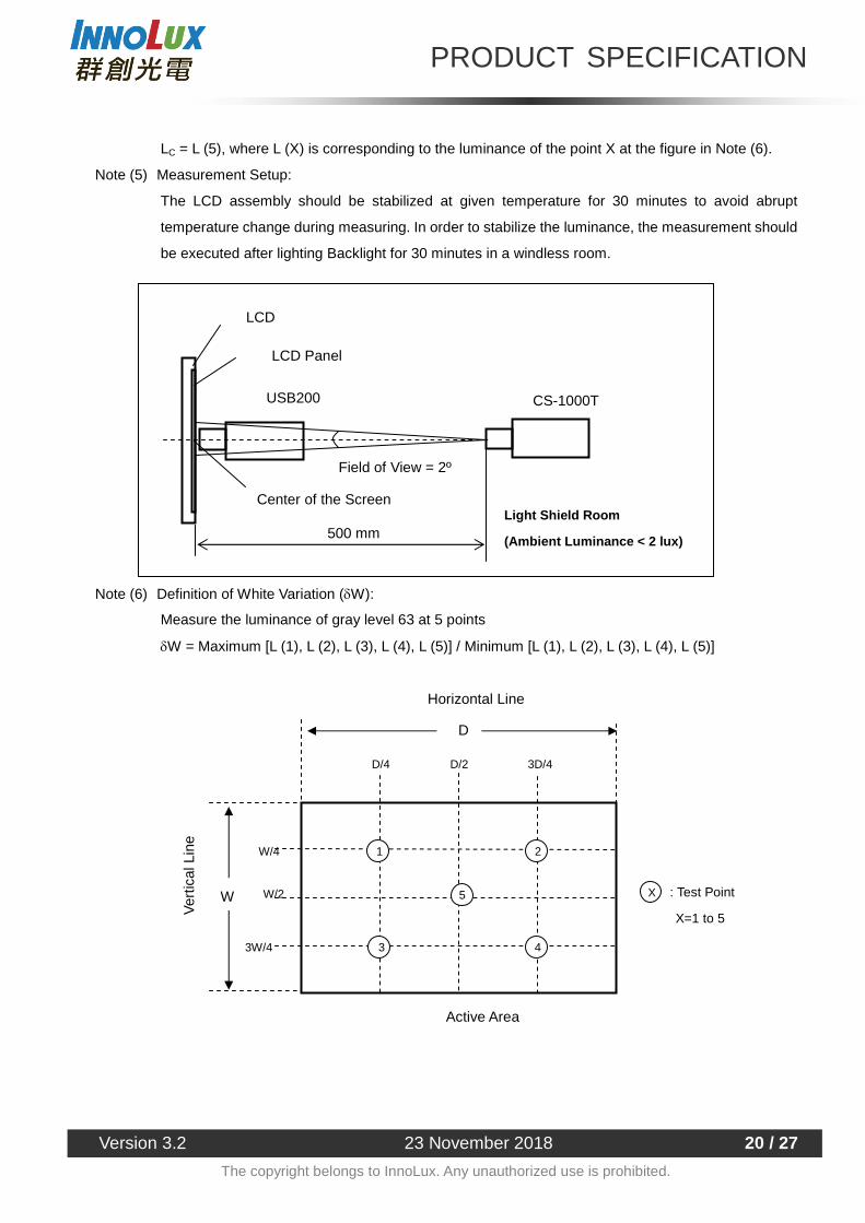
Note (5) Measurement Setup:
The LCD assembly should be stabilized at given temperature for 30 minutes to avoid abrupt
temperature change during measuring. In order to stabilize the luminance, the measurement should
be executed after lighting Backlight for 30 minutes in a windless room.
Note (6) Definition of White Variation (δW):
Measure the luminance of gray level 63 at 5 points
δW = Maximum [L (1), L (2), L (3), L (4), L (5)] / Minimum [L (1), L (2), L (3), L (4), L (5)]
D
W
Active Area
Ver
tical
Lin
e
Horizontal Line
: Test Point
X=1 to 5
5
1 2
3 4
D/4 D/2 3D/4
W/4
W/2
3W/4
X
CS-1000T
Field of View = 2º
500 mm
LCD
LCD Panel
Center of the Screen Light Shield Room
(Ambient Luminance < 2 lux)
USB200
PRODUCT SPECIFICATION
Version 3.2 23 November 2018 21 / 27
The copyright belongs to InnoLux. Any unauthorized use is prohibited.
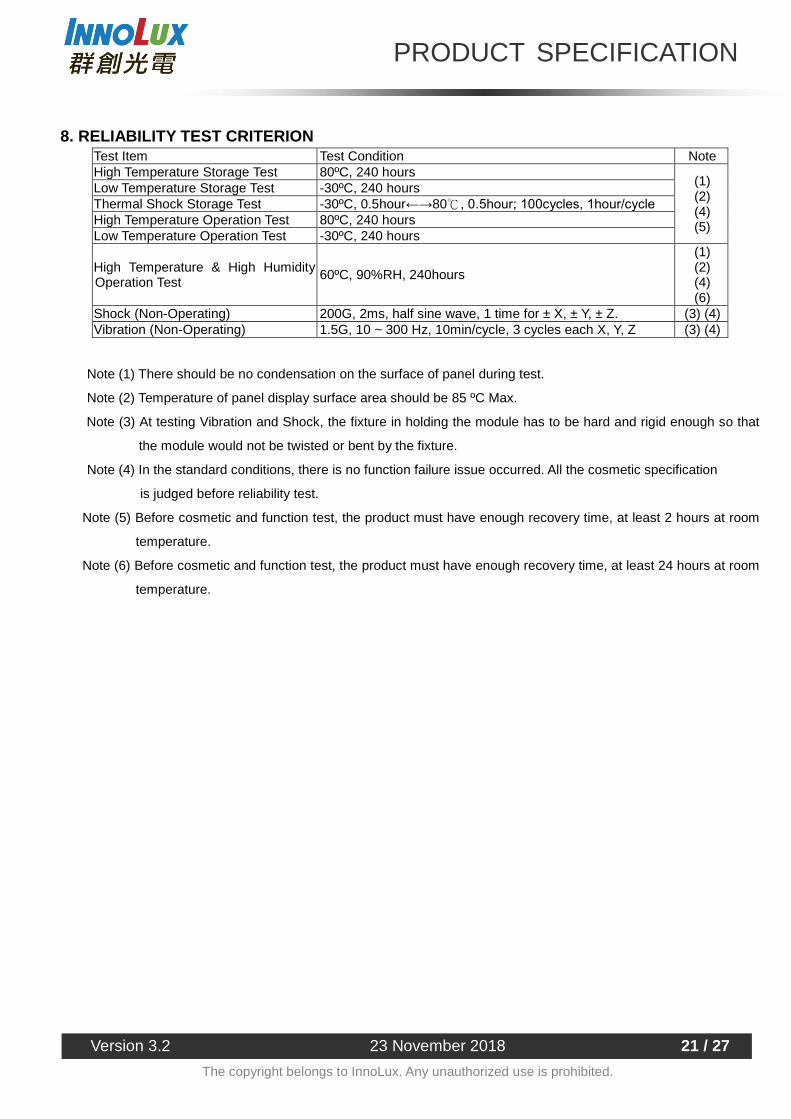
8. RELIABILITY TEST CRITERION Test Item Test Condition Note High Temperature Storage Test 80ºC, 240 hours
(1) (2) (4) (5)
Low Temperature Storage Test -30ºC, 240 hours Thermal Shock Storage Test - ℃30ºC, 0.5hour←→80 , 0.5hour; 100cycles, 1hour/cycle High Temperature Operation Test 80ºC, 240 hours Low Temperature Operation Test -30ºC, 240 hours
High Temperature & High Humidity Operation Test
60ºC, 90%RH, 240hours
(1) (2) (4) (6)
Shock (Non-Operating) 200G, 2ms, half sine wave, 1 time for ± X, ± Y, ± Z. (3) (4) Vibration (Non-Operating) 1.5G, 10 ~ 300 Hz, 10min/cycle, 3 cycles each X, Y, Z (3) (4)
Note (1) There should be no condensation on the surface of panel during test.
Note (2) Temperature of panel display surface area should be 85 ºC Max.
Note (3) At testing Vibration and Shock, the fixture in holding the module has to be hard and rigid enough so that
the module would not be twisted or bent by the fixture.
Note (4) In the standard conditions, there is no function failure issue occurred. All the cosmetic specification
is judged before reliability test.
Note (5) Before cosmetic and function test, the product must have enough recovery time, at least 2 hours at room
temperature.
Note (6) Before cosmetic and function test, the product must have enough recovery time, at least 24 hours at room
temperature.
PRODUCT SPECIFICATION
Version 3.2 23 November 2018 22 / 27
The copyright belongs to InnoLux. Any unauthorized use is prohibited.
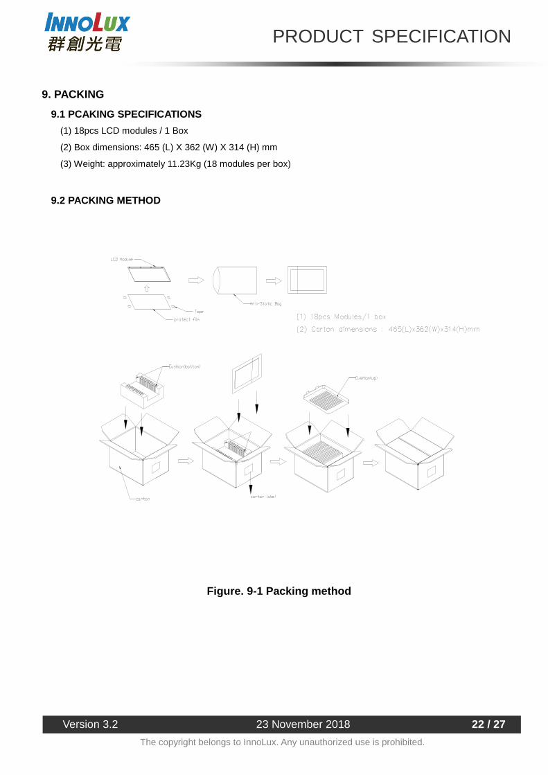
9. PACKING
9.1 PCAKING SPECIFICATIONS
(1) 18pcs LCD modules / 1 Box
(2) Box dimensions: 465 (L) X 362 (W) X 314 (H) mm
(3) Weight: approximately 11.23Kg (18 modules per box)
9.2 PACKING METHOD
Figure. 9-1 Packing method
PRODUCT SPECIFICATION
Version 3.2 23 November 2018 23 / 27
The copyright belongs to InnoLux. Any unauthorized use is prohibited.
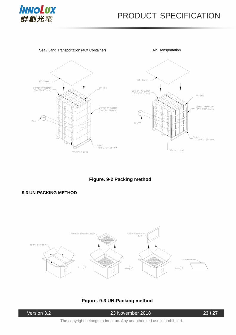
Sea / Land Transportation (40ft Container) Air Transportation
9.3 UN-PACKING METHOD
Figure. 9-2 Packing method
Figure. 9-3 UN-Packing method
PRODUCT SPECIFICATION
Version 3.2 23 November 2018 24 / 27
The copyright belongs to InnoLux. Any unauthorized use is prohibited.
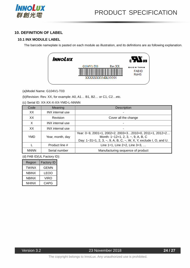
10. DEFINITION OF LABEL
10.1 INX MODULE LABEL
The barcode nameplate is pasted on each module as illustration, and its definitions are as following explanation.
(a)Model Name: G104V1-T03
(b)Revision: Rev. XX, for example: A0, A1… B1, B2… or C1, C2…etc.
(c) Serial ID: XX-XX-X-XX-YMD-L-NNNN
Code Meaning Description
XX INX internal use -
XX Revision Cover all the change
X INX internal use -
XX INX internal use -
YMD Year, month, day Year: 0~9, 2001=1, 2002=2, 2003=3…2010=0, 2011=1, 2012=2…
Month: 1~12=1, 2, 3, ~, 9, A, B, C Day: 1~31=1, 2, 3, ~, 9, A, B, C, ~, W, X, Y, exclude I, O, and U.
L Product line # Line 1=1, Line 2=2, Line 3=3, …
NNNN Serial number Manufacturing sequence of product
(d) FAB ID(UL Factory ID):
Region Factory ID
TWINX GEMN
NBINX LEOO
NBINX VIRO
NHINX CAPG
PRODUCT SPECIFICATION
Version 3.2 23 November 2018 25 / 27
The copyright belongs to InnoLux. Any unauthorized use is prohibited.
11. PRECAUTIONS
11.1 ASSEMBLY AND HANDLING PRECAUTIONS
(1) Do not apply rough force such as bending or twisting to the module during assembly.
(2) To assemble or install module into user’s system can be only in clean working areas. The dust and oil
may cause electrical short or worsen the polarizer.
(3) It’s not permitted to have pressure or impulse on the module because the LCD panel and Backlight will be
damaged.
(4) Always follow the correct power sequence when LCD module is connecting and operating. This can
prevent damage to the CMOS LSI chips during latch-up.
(5) Do not pull the I/F connector in or out while the module is operating.
(6) Do not disassemble the module.
(7) Use a soft dry cloth without chemicals for cleaning, because the surface of polarizer is very soft and
easily scratched.
(8) It is dangerous that moisture come into or contacted the LCD module, because moisture may damage
LCD module when it is operating.
(9) High temperature or humidity may reduce the performance of module. Please store LCD module within
the specified storage conditions.
(10) When ambient temperature is lower than 10ºC may reduce the display quality, the response time will
become slowly.
(11) Do not keep same pattern in a long period of time. It may cause image sticking on LCD.
11.2 SAFETY PRECAUTIONS
(1) Do not disassemble the module or insert anything into the Backlight unit.
(2) If the liquid crystal material leaks from the panel, it should be kept away from the eyes or mouth. In case
of contact with hands, skin or clothes, it has to be washed away thoroughly with soap.
(3) After the module’s end of life, it is not harmful in case of normal operation and storage.
PRODUCT SPECIFICATION
Version 3.2 23 November 2018 26 / 27
The copyright belongs to InnoLux. Any unauthorized use is prohibited.
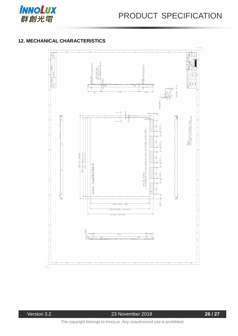
12. MECHANICAL CHARACTERISTICS

PRODUCT SPECIFICATION
Version 3.2 23 November 2018 27 / 27
The copyright belongs to InnoLux. Any unauthorized use is prohibited.
Our company network supports you worldwide with offices in Germany, Austria, Switzerland, the UK and the USA. For more information please contact:
Headquarters
Germany
FORTEC Elektronik AG Lechwiesenstr. 9 86899 Landsberg am Lech Phone: +49 8191 91172-0 E-Mail: [email protected] Internet: www.fortecag.de
Fortec Group Members
Austria
FORTEC Elektronik AG Office Vienna Nuschinggasse 12 1230 Wien Phone: +43 1 8673492-0 E-Mail: [email protected] Internet: www.fortec.at
Germany
Distec GmbH Augsburger Str. 2b 82110 Germering Phone: +49 89 894363-0 E-Mail: [email protected] Internet: www.distec.de
Switzerland
ALTRAC AG Bahnhofstraße 3 5436 Würenlos Phone: +41 44 7446111 E-Mail: [email protected] Internet: www.altrac.ch
United Kingdom
Display Technology Ltd. Osprey House, 1 Osprey Court Hichingbrooke Business Park Huntingdon, Cambridgeshire, PE29 6FN Phone: +44 1480 411600 E-Mail: [email protected] Internet: www. displaytechnology.co.uk
USA
Apollo Display Technologies, Corp. 87 Raynor Avenue, Unit 1Ronkonkoma, NY 11779 Phone: +1 631 5804360 E-Mail: [email protected] Internet: www.apollodisplays.com


![11X1 T03 03 symmetry [2011]](https://img.pdfslide.us/doc/110x75/559cd2df1a28ab607f8b477a/11x1-t03-03-symmetry-2011.jpg)