Embed Size (px)
Citation preview
Document Number: DOD-PD-0202 (6th edition)Published date: September 2003 CP(N)
1 NEC LCD Technologies, Ltd.2002, 2003 All rights reserved.
This DATA SHEET is updated document fromDOD-M-1255(5).
All information is subject to change without notice.Please confirm the sales representative beforestarting to design your system.
TFT COLOR LCD MODULE
NL10276BC20-04
26.3cm (10.4 Type)XGA
DATA SHEETDOD-PD-0202 (6th edition)
NL10276BC20-04
DATA SHEET DOD-PD-0202 (6th edition) 2
INTRODUCTION
No part of this document shall be copied in any form or by any means without the prior written consentof NEC LCD Technologies, Ltd. (hereinafter called "NEC").
NEC does not assume any liability for infringement of patents, copyrights or other intellectual propertyrights of third parties by or arising from use of a product described herein or any other liability arisingfrom use of such application. No license, express, implied or otherwise, is granted under any patents,copyrights or other intellectual property rights of NEC or of others.
While NEC has been making continuous effort to enhance the reliability of its products, the possibilityof failures cannot be eliminated entirely. To minimize risks of damage to property or injury to personarising from a failure in an NEC product, customers must incorporate sufficient safety measures in theirdesign, such as redundancy, fire-containment and anti-failure features.
NEC products are classified into the following three quality grades:" S t a n d a r d " , " S p e c i a l " , " S p e c i f i c "
The "Specific" quality grade applies only to applications developed based on a customer designated"quality assurance program" for a specific application. The recommended applications of a productdepend on its quality grade, as indicated below. Customers must check the quality grade of eachapplication before using it in a particular application.
Standard: Computers, office equipment, communications equipment, test and measurement equipment,audio and visual equipment, home electronic appliances, machine tools, personal electronicequipment and industrial robots
Special: Transportation equipment (automobiles, trains, ships, etc.), traffic control systems, anti-disastersystems, anti-crime systems, safety equipment and medical equipment (not specificallydesigned for life support)
Specific: Military systems, aircraft, aerospace equipment, submersible repeaters, nuclear reactor controlsystems, life support systems (medical equipment, etc.) and any other equipment
The quality grade of this product is "Standard" unless otherwise specified in this document. Ifcustomers intend to use this product for applications other than those specified for "Standard" qualitygrade, they should contact NEC sales representative in advance.
NL10276BC20-04
DATA SHEET DOD-PD-0202 (6th edition) 3
CONTENTS
INTRODUCTION ..........................................................................................................................................2
1. OUTLINE....................................................................................................................................................51.1 STRUCTURE AND PRINCIPLE...........................................................................................................51.2 APPLICATIONS.....................................................................................................................................51.3 FEATURES.............................................................................................................................................5
2. GENERAL SPECIFICATIONS ................................................................................................................63. BLOCK DIAGRAM...................................................................................................................................74. DETAILED SPECIFICATIONS ...............................................................................................................8
4.1 MECHANICAL SPECIFICATIONS......................................................................................................84.2 ABSOLUTE MAXIMUM RATINGS ....................................................................................................84.3 ELECTRICAL CHARACTERISTICS...................................................................................................9
4.3.1 Driving for LCD panel signal processing board ............................................................................94.3.2 Working for backlight lamp ...........................................................................................................94.3.3 Power supply voltage ripple.........................................................................................................104.3.4 Fuses ............................................................................................................................................10
4.4 POWER SUPPLY VOLTAGE SEQUENCE ........................................................................................114.4.1 Sequence for LCD panel signal processing board .......................................................................114.4.2 Sequence for backlight inverter (Option).....................................................................................11
4.5 CONNECTIONS AND FUNCTIONS FOR INTERFACE PINS.........................................................124.5.1 LCD panel signal processing board .............................................................................................124.5.2 Backlight lamp.............................................................................................................................134.5.3 Positions of a plug and a socket...................................................................................................134.5.4 Connection between receiver and transmitter for LVDS .............................................................14
4.6 DISPLAY COLORS AND INPUT DATA SIGNALS ..........................................................................154.7 DISPLAY POSITIONS.........................................................................................................................164.8 SCANNING DIRECTIONS .................................................................................................................164.9 INPUT SIGNAL TIMINGS FOR LCD PANEL SIGNAL PROCESSING BOARD ...........................17
4.9.1 Outline of input signal timings ....................................................................................................174.9.2 Input signal timing chart ..............................................................................................................174.9.3 Timing characteristics ..................................................................................................................18
4.10 OPTICS...............................................................................................................................................194.10.1 Optical characteristics................................................................................................................194.10.2 Definition of contrast ratio.........................................................................................................204.10.3 Definition of luminance uniformity ...........................................................................................204.10.4 Definition of response times ......................................................................................................204.10.5 Definition of viewing angles......................................................................................................20
NL10276BC20-04
DATA SHEET DOD-PD-0202 (6th edition) 4
CONTENTS
5. RELIABILITY TESTS.............................................................................................................................216. PRECAUTIONS .......................................................................................................................................22
6.1 MEANING OF CAUTION SIGNS ......................................................................................................226.2 CAUTIONS ..........................................................................................................................................226.3 ATTENTIONS ......................................................................................................................................22
6.3.1 Handling of the product ...............................................................................................................226.3.2 Environment.................................................................................................................................236.3.3 Characteristics..............................................................................................................................236.3.4 Other ............................................................................................................................................23
7. OUTLINE DRAWINGS ...........................................................................................................................247.1 FRONT VIEW......................................................................................................................................247.2 REAR VIEW ........................................................................................................................................25
NL10276BC20-04
DATA SHEET DOD-PD-0202 (6th edition) 5
1. OUTLINE
1.1 STRUCTURE AND PRINCIPLE
NL10276BC20-04 module is composed of the amorphous silicon thin film transistor liquid crystaldisplay (a-Si TFT LCD) panel structure with driver LSIs for driving the TFT (Thin Film Transistor) arrayand a backlight unit.The a-Si TFT LCD panel structure is injected liquid crystal material into a narrow gap between the TFT
array glass substrate and a color-filter glass substrate.Color (Red, Green, Blue) data signals from a host system (e.g. PC, signal generator, etc.) are modulated
into best form for active matrix system by a signal processing board, and sent to the driver LSIs whichdrive the individual TFT arrays.The TFT array as an electro-optical switch regulates the amount of transmitted light from the backlight
assembly, when it is controlled by data signals. Color images are created by regulating the amount oftransmitted light through the TFT array of red, green and blue dots.
1.2 APPLICATIONS
• Display terminal for control system• Industrial PC
1.3 FEATURES
• High luminance• Wide viewing angle• Extensive temperature• 6-bit digital RGB signals• Single link LVDS interface• Reversible-scan direction• Edge light type• Replaceable lamp for backlight unit (Inverter less)• Acquisition product for UL1950 3rd edition/CSA C22.2 No.950-95 (File number: E170632)
NL10276BC20-04
DATA SHEET DOD-PD-0202 (6th edition) 6
2. GENERAL SPECIFICATIONS
Display area 210.4 (W) × 157.8 (H) mm (typ.)
Diagonal size of display 26.3 cm (10.4 inches)
Drive system a-Si TFT active matrix
Display color 262,144 colors
Pixel 1,024 (H) × 768 (V) pixels
Pixel arrangement RGB (Red dot, Green dot, Blue dot) vertical stripe
Dot pitch 0.0685 (W) × 0.2055 (H) mm
Pixel pitch 0.2055 (W) × 0.2055 (H) mm
Module size 243.0 (W) × 185.1 (H) × 11.0 (D) mm (typ.)
Weight 530 g (typ.)
Contrast ratio 300:1 (typ.)
Viewing angle At the contrast ratio 10:1• Horizontal: Left side 60° (typ.), Right side 60° (typ.)• Vertical: Up side 45° (typ.), Down side 60° (typ.)
Designed viewing direction At DPSR: normal scan• Viewing direction without image reversal: up side (12 o'clock)• Viewing direction with contrast peak: down side 5° to 10° (6 o'clock)• Viewing angle with optimum grayscale (γ=2.2): normal axis
Polarizer surface Non matt treatment
Polarizer pencil-hardness 3H (min.) [by JIS K5400]
Color gamut At LCD panel center40 % (typ.) [against NTSC color space]
Response time Ton (White 90% → Black 10%)15 ms (typ.)
Luminance At 5.0mArms / lamp300 cd/m2 (typ.)
Signal system Single link LVDS (Receiver: THC63LVDF64A, THine Electronics Inc.)[6-bit digital signals for data of RGB colors,Dot clock (CLK), Data enable (DE)]
Power supply voltage LCD panel signal processing board: 3.3V
Backlight Edge light type: 2 cold cathode fluorescent lamps
Replaceable parts• Lamps for backlight unit: Type No. 104LHS35
Recommended inverter (Option)• Inverter: Type No. 104PW191
Power consumption At maximum luminance and checkered flag pattern6.2W (typ., Power dissipation of the inverter does not include.)
NL10276BC20-04
DATA SHEET DOD-PD-0202 (6th edition) 7
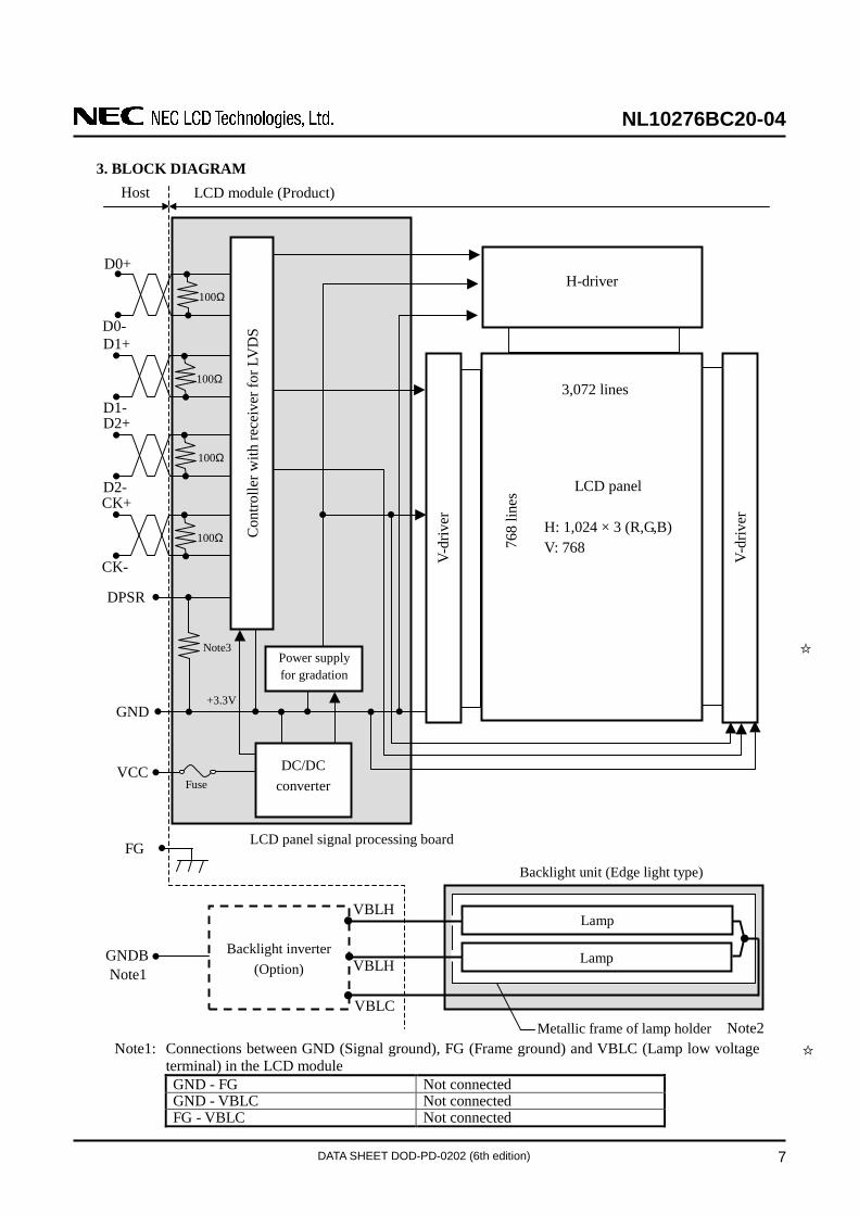
3. BLOCK DIAGRAM
Note1: Connections between GND (Signal ground), FG (Frame ground) and VBLC (Lamp low voltageterminal) in the LCD moduleGND - FG Not connectedGND - VBLC Not connectedFG - VBLC Not connected
Host
V-dr
iver
3,072 lines
LCD panel
H: 1,024 × 3 (R,G,B)V: 76876
8 lin
es
VCC
GND
Power supplyfor gradation
DC/DCconverter
LCD module (Product)
LCD panel signal processing board
V-dr
iver
D0+
+3.3V
D0-
Con
trolle
r with
rece
iver
for L
VD
S
D1+
D1-D2+
D2-CK+
CK-
100Ω
100Ω
100Ω
100Ω
DPSR
Fuse
Backlight inverter(Option) VBLH
VBLH
GNDB
VBLC
Backlight unit (Edge light type)
Note1Lamp
Lamp
Metallic frame of lamp holder Note2
H-driver
FG
Note3
NL10276BC20-04
DATA SHEET DOD-PD-0202 (6th edition) 8
Note2: GND, FG and GNDB must be connected to customer equipment's ground, and it isrecommended that these grounds are connected together in customer equipment.
Note3: Pull-down resistance of DPSR pin(kΩ)
min. typ. max.20 50 132
4. DETAILED SPECIFICATIONS
4.1 MECHANICAL SPECIFICATIONS
Parameter Specification Unit
Module size 243.0 ± 0.5 (W) × 185.1 ± 0.5 (H) × 11.0 ± 0.5 (D) Note1 mm
Display area 210.4 ± 0.5 (W) × 157.8 ± 0.5 (H) Note1 mm
Weight 530 (typ.), 550 (max.) g
Note1: See "11. OUTLINE DRAWINGS".
4.2 ABSOLUTE MAXIMUM RATINGS
Parameter Symbol Rating Unit Remarks
LCD panel signal board VCC -0.3 to +4.0 VPower supply
voltage Lamp voltageNote1 VBLH 1,500 Vrms
Display signalsNote2 VD -0.3 to VCC+0.3 V
Input voltagefor signals Function signals
Note3 VF -0.3 to VCC+0.3 V
Ta = 25°C
Storage temperature Tst -20 to +70 °C
Front surface TopF 0 to +60 °COperating temperature
Rear surface TopR 0 to +60 °C
-
≤ 95 % Ta ≤ 40°C
≤ 85 % 40 < Ta ≤ 50°C
≤ 70 % 50 < Ta ≤ 55°C
Relative humidityNote4 RH
≤ 60 % 55 < Ta ≤ 60°C
Absolute humidityNote4 AH ≤ 78
Note5 g/m3 Ta > 60°C
Note1: "VBLH" is the voltage value between low voltage terminal (Cold) and high voltage terminal (Hot).Note2: Display signals are D0+/-, D1+/-, D2+/- and CK+/-. Also controller with LVDS receiver are
worked by +3.3V from DC/DC converter.Note3: Function signal is DPSR.Note4: No condensationNote5: Ta = 60°C, RH = 60%
NL10276BC20-04
DATA SHEET DOD-PD-0202 (6th edition) 9
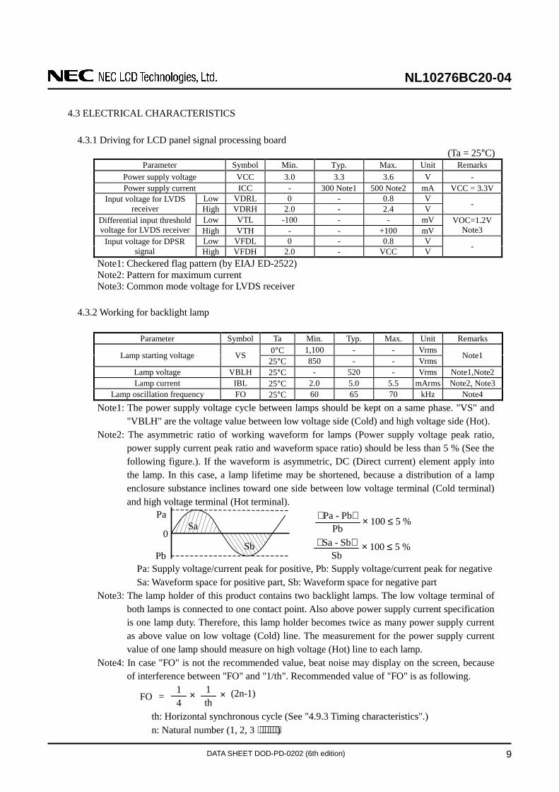
4.3 ELECTRICAL CHARACTERISTICS
4.3.1 Driving for LCD panel signal processing board(Ta = 25°C)
Parameter Symbol Min. Typ. Max. Unit RemarksPower supply voltage VCC 3.0 3.3 3.6 V -Power supply current ICC - 300 Note1 500 Note2 mA VCC = 3.3V
Low VDRL 0 - 0.8 VInput voltage for LVDSreceiver High VDRH 2.0 - 2.4 V -
Low VTL -100 - - mVDifferential input thresholdvoltage for LVDS receiver High VTH - - +100 mV
VOC=1.2VNote3
Low VFDL 0 - 0.8 VInput voltage for DPSRsignal High VFDH 2.0 - VCC V -
Note1: Checkered flag pattern (by EIAJ ED-2522)Note2: Pattern for maximum currentNote3: Common mode voltage for LVDS receiver
4.3.2 Working for backlight lamp
Parameter Symbol Ta Min. Typ. Max. Unit Remarks0°C 1,100 - - VrmsLamp starting voltage VS
25°C 850 - - VrmsNote1
Lamp voltage VBLH 25°C - 520 - Vrms Note1,Note2Lamp current IBL 25°C 2.0 5.0 5.5 mArms Note2, Note3
Lamp oscillation frequency FO 25°C 60 65 70 kHz Note4Note1: The power supply voltage cycle between lamps should be kept on a same phase. "VS" and
"VBLH" are the voltage value between low voltage side (Cold) and high voltage side (Hot).Note2: The asymmetric ratio of working waveform for lamps (Power supply voltage peak ratio,
power supply current peak ratio and waveform space ratio) should be less than 5 % (See thefollowing figure.). If the waveform is asymmetric, DC (Direct current) element apply intothe lamp. In this case, a lamp lifetime may be shortened, because a distribution of a lampenclosure substance inclines toward one side between low voltage terminal (Cold terminal)and high voltage terminal (Hot terminal).
Pa: Supply voltage/current peak for positive, Pb: Supply voltage/current peak for negativeSa: Waveform space for positive part, Sb: Waveform space for negative part
Note3: The lamp holder of this product contains two backlight lamps. The low voltage terminal ofboth lamps is connected to one contact point. Also above power supply current specificationis one lamp duty. Therefore, this lamp holder becomes twice as many power supply currentas above value on low voltage (Cold) line. The measurement for the power supply currentvalue of one lamp should measure on high voltage (Hot) line to each lamp.
Note4: In case "FO" is not the recommended value, beat noise may display on the screen, becauseof interference between "FO" and "1/th". Recommended value of "FO" is as following.
th: Horizontal synchronous cycle (See "4.9.3 Timing characteristics".)n: Natural number (1, 2, 3 ⋅⋅⋅⋅⋅⋅⋅⋅)
FO =14
1th
× × (2n-1)
Pa
Pb
Sa
Sb0
Pa - PbPb
× 100 ≤ 5 %
Sa - SbSb
× 100 ≤ 5 %
NL10276BC20-04
DATA SHEET DOD-PD-0202 (6th edition) 10
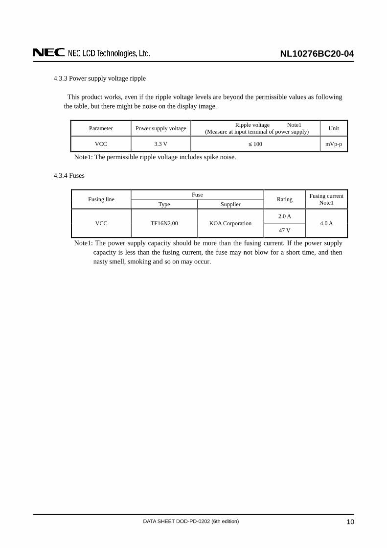
4.3.3 Power supply voltage ripple
This product works, even if the ripple voltage levels are beyond the permissible values as followingthe table, but there might be noise on the display image.
Parameter Power supply voltage Ripple voltage Note1 (Measure at input terminal of power supply) Unit
VCC 3.3 V ≤ 100 mVp-p
Note1: The permissible ripple voltage includes spike noise.
4.3.4 Fuses
FuseFusing line
Type SupplierRating Fusing current
Note1
2.0 AVCC TF16N2.00 KOA Corporation
47 V4.0 A
Note1: The power supply capacity should be more than the fusing current. If the power supplycapacity is less than the fusing current, the fuse may not blow for a short time, and thennasty smell, smoking and so on may occur.
NL10276BC20-04
DATA SHEET DOD-PD-0202 (6th edition) 11
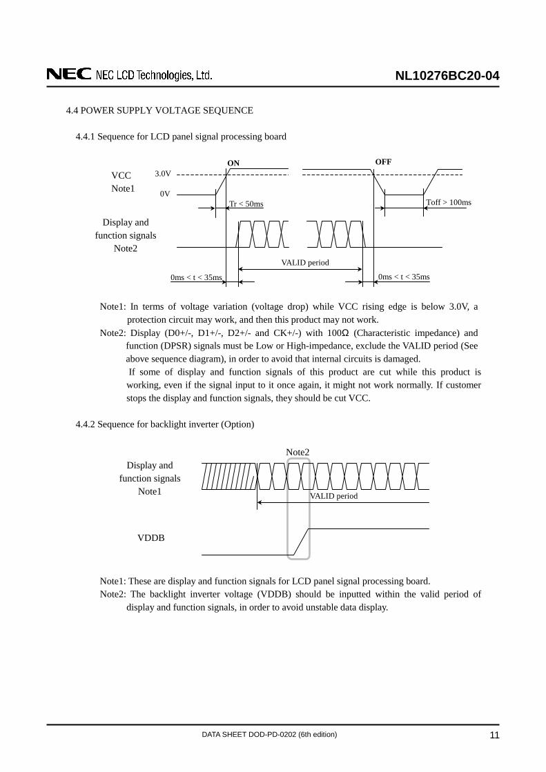
4.4 POWER SUPPLY VOLTAGE SEQUENCE
4.4.1 Sequence for LCD panel signal processing board
Note1: In terms of voltage variation (voltage drop) while VCC rising edge is below 3.0V, aprotection circuit may work, and then this product may not work.
Note2: Display (D0+/-, D1+/-, D2+/- and CK+/-) with 100Ω (Characteristic impedance) andfunction (DPSR) signals must be Low or High-impedance, exclude the VALID period (Seeabove sequence diagram), in order to avoid that internal circuits is damaged.If some of display and function signals of this product are cut while this product isworking, even if the signal input to it once again, it might not work normally. If customerstops the display and function signals, they should be cut VCC.
4.4.2 Sequence for backlight inverter (Option)
Note1: These are display and function signals for LCD panel signal processing board.Note2: The backlight inverter voltage (VDDB) should be inputted within the valid period of
display and function signals, in order to avoid unstable data display.
VALID period
OFF
0ms < t < 35ms 0ms < t < 35ms
ON3.0V
0VTr < 50ms
VCCNote1
Display andfunction signals
Note2
Toff > 100ms
Display andfunction signals
Note1
VDDB
VALID period
Note2
NL10276BC20-04
DATA SHEET DOD-PD-0202 (6th edition) 12
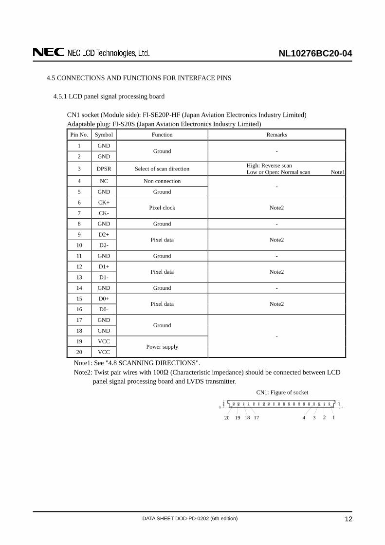
4.5 CONNECTIONS AND FUNCTIONS FOR INTERFACE PINS
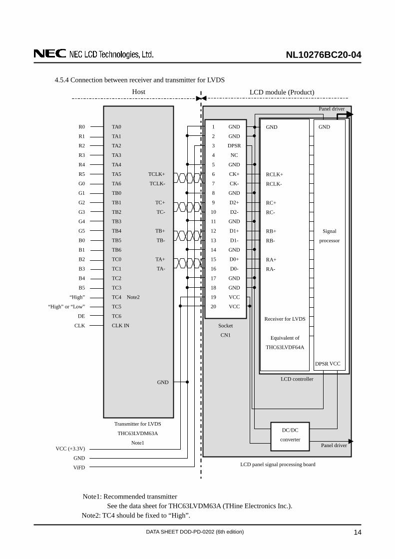
4.5.1 LCD panel signal processing board
CN1 socket (Module side): FI-SE20P-HF (Japan Aviation Electronics Industry Limited)Adaptable plug: FI-S20S (Japan Aviation Electronics Industry Limited)
Pin No. Symbol Function Remarks
1 GND
2 GNDGround -
3 DPSR Select of scan direction High: Reverse scanLow or Open: Normal scan Note1
4 NC Non connection
5 GND Ground-
6 CK+
7 CK-Pixel clock Note2
8 GND Ground -
9 D2+
10 D2-Pixel data Note2
11 GND Ground -
12 D1+
13 D1-Pixel data Note2
14 GND Ground -
15 D0+
16 D0-Pixel data Note2
17 GND
18 GNDGround
19 VCC
20 VCCPower supply
-
Note1: See "4.8 SCANNING DIRECTIONS".Note2: Twist pair wires with 100Ω (Characteristic impedance) should be connected between LCD
panel signal processing board and LVDS transmitter.CN1: Figure of socket
20 19 18 17 4 3 2 1
NL10276BC20-04
DATA SHEET DOD-PD-0202 (6th edition) 13
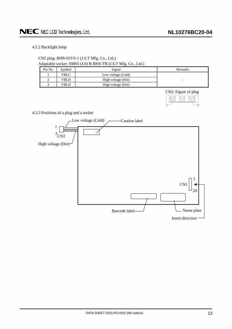
4.5.2 Backlight lamp
CN2 plug: BHR-03VS-1 (J.S.T Mfg. Co., Ltd.)Adaptable socket: SM03 (4.0) B-BHS-TB (J.S.T Mfg. Co., Ltd.)
Pin No. Symbol Signal Remarks1 VBLC Low voltage (Cold)2 VBLH High voltage (Hot)3 VBLH High voltage (Hot)
-
4.5.3 Positions of a plug and a socket
CN2: Figure of plug
1 3
CN11
20
Barcode label Name plate
CN2
Caution labelLow voltage (Cold)
High voltage (Hot)
13
Insert direction
NL10276BC20-04
DATA SHEET DOD-PD-0202 (6th edition)
4.5.4 Connection between receiver and transmitter for LVDS
Note1: Recommended transmitterSee the data sheet for THC63LVDM63A (THine Electronics Inc.).
Note2: TC4 should be fixed to “High”.
R0
R1
R2
R3
R4
R5
G0
G1
G2
G3
G4
G5
B0
B1
B2
B3
B4
B5
“High”
“High” or “Low”
DE
CLK
VCC (+3.3V)
GND
ViFD
GND
GND
DPSR
NC
GND
CK+
CK-
GND
D2+
D2-
GND
D1+
D1-
GND
D0+
D0-
GND
GND
VCC
VCC
TA0
TA1
TA2
TA3
TA4
TA5
TA6
TB0
TB1
TB2
TB3
TB4
TB5
TB6
TC0
TC1
TC2
TC3
TC4 Note2
TC5
TC6
CLK IN
TCLK+
TCLK-
TC+
TC-
TB+
TB-
TA+
TA-
1
2
3
4
5
6
7
8
9
10
11
12
13
14
15
16
17
18
19
20
GND
Transmitter for LVDS
THC63LVDM63A
Note1
Socket
CN1
DC/DC
converter
LCD panel signal processing board
Host LCD module (Product)
GND
RCLK+
RCLK-
RC+
RC-
RB+
RB-
RA+
RA-
LCD controller
Receiver for LVDS
Equivalent of
THC63LVDF64A
Panel driver
GND
Signal
processor
VCCDPSR
14
Panel driver
NL10276BC20-04
DATA SHEET DOD-PD-0202 (6th edition) 15
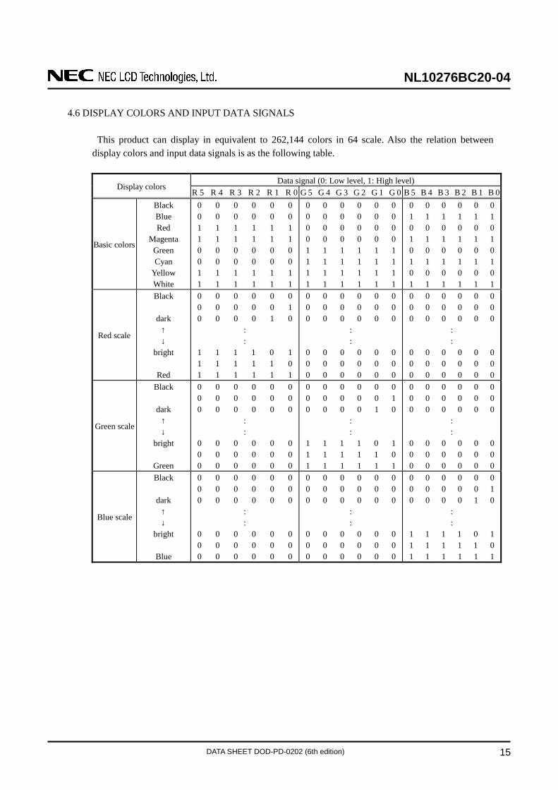
4.6 DISPLAY COLORS AND INPUT DATA SIGNALS
This product can display in equivalent to 262,144 colors in 64 scale. Also the relation betweendisplay colors and input data signals is as the following table.
Data signal (0: Low level, 1: High level)Display colors
R 5 R 4 R 3 R 2 R 1 R 0 G 5 G 4 G 3 G 2 G 1 G 0 B 5 B 4 B 3 B 2 B 1 B 0
Basic colors
BlackBlueRed
MagentaGreenCyan
YellowWhite
0 0 0 0 0 00 0 0 0 0 01 1 1 1 1 11 1 1 1 1 10 0 0 0 0 00 0 0 0 0 01 1 1 1 1 11 1 1 1 1 1
0 0 0 0 0 00 0 0 0 0 00 0 0 0 0 00 0 0 0 0 01 1 1 1 1 11 1 1 1 1 11 1 1 1 1 11 1 1 1 1 1
0 0 0 0 0 01 1 1 1 1 10 0 0 0 0 01 1 1 1 1 10 0 0 0 0 01 1 1 1 1 10 0 0 0 0 01 1 1 1 1 1
Red scale
Black
dark↑↓
bright
Red
0 0 0 0 0 00 0 0 0 0 10 0 0 0 1 0
::
1 1 1 1 0 11 1 1 1 1 01 1 1 1 1 1
0 0 0 0 0 00 0 0 0 0 00 0 0 0 0 0
::
0 0 0 0 0 00 0 0 0 0 00 0 0 0 0 0
0 0 0 0 0 00 0 0 0 0 00 0 0 0 0 0
::
0 0 0 0 0 00 0 0 0 0 00 0 0 0 0 0
Green scale
Black
dark↑↓
bright
Green
0 0 0 0 0 00 0 0 0 0 00 0 0 0 0 0
::
0 0 0 0 0 00 0 0 0 0 00 0 0 0 0 0
0 0 0 0 0 00 0 0 0 0 10 0 0 0 1 0
::
1 1 1 1 0 11 1 1 1 1 01 1 1 1 1 1
0 0 0 0 0 00 0 0 0 0 00 0 0 0 0 0
::
0 0 0 0 0 00 0 0 0 0 00 0 0 0 0 0
Blue scale
Black
dark↑↓
bright
Blue
0 0 0 0 0 00 0 0 0 0 00 0 0 0 0 0
::
0 0 0 0 0 00 0 0 0 0 00 0 0 0 0 0
0 0 0 0 0 00 0 0 0 0 00 0 0 0 0 0
::
0 0 0 0 0 00 0 0 0 0 00 0 0 0 0 0
0 0 0 0 0 00 0 0 0 0 10 0 0 0 1 0
::
1 1 1 1 0 11 1 1 1 1 01 1 1 1 1 1
NL10276BC20-04
DATA SHEET DOD-PD-0202 (6th edition) 16
4.7 DISPLAY POSITIONS
The following table is the coordinates per pixel (See figure of "4.8 SCANNING DIRECTIONS".).
C( 0, 0) C( 1, 0) • • • C( X, 0) • • • C(1022, 0) C(1023, 0)
C( 0, 1) C( 1, 1) • • • C( X, 1) • • • C(1022, 1) C(1023, 1)
•••
•••
•• • •
•
•••
•• • •
•
•••
•• • •
•C( 0, Y) C( 1, Y) • • • C( X, Y) • • • C(1022, Y) C(1023, Y)
•••
•••
•• • •
•
•••
•• • •
•
•••
•••
C( 0, 766) C( 1, 766) • • • C( X, 766) • • • C(1022, 766) C(1023, 766)
C( 0, 767) C( 1, 767) • • • C( X, 767) • • • C(1022, 767) C(1023, 767)
4.8 SCANNING DIRECTIONS
The following figures are seen from a front view. Also the arrow shows the direction of scan.
Note1: Meaning of C (X, Y) and D (X, Y)C (X, Y): The coordinates of the display position (See "4.7 DISPLAY POSITIONS".)D (X, Y): The data number of input signal for LCD panel signal processing board
Figure 1. Normal scan (DPSR: Low or Open)
C (0,0)
D (0,0)
C (0,767)
D (0,767)
C (1023,767)
D (1023,767)
C (1023,0)
D (1023,0)
Figure 2. Reverse scan (DPSR: High)
C (0,0)
D (1023,767)
C (0,767)
D (1023,0)
C (1023,767)
D (0,0)
C (1023,0)
D (0,767)
Note1
Note1
NL10276BC20-04
DATA SHEET DOD-PD-0202 (6th edition) 17
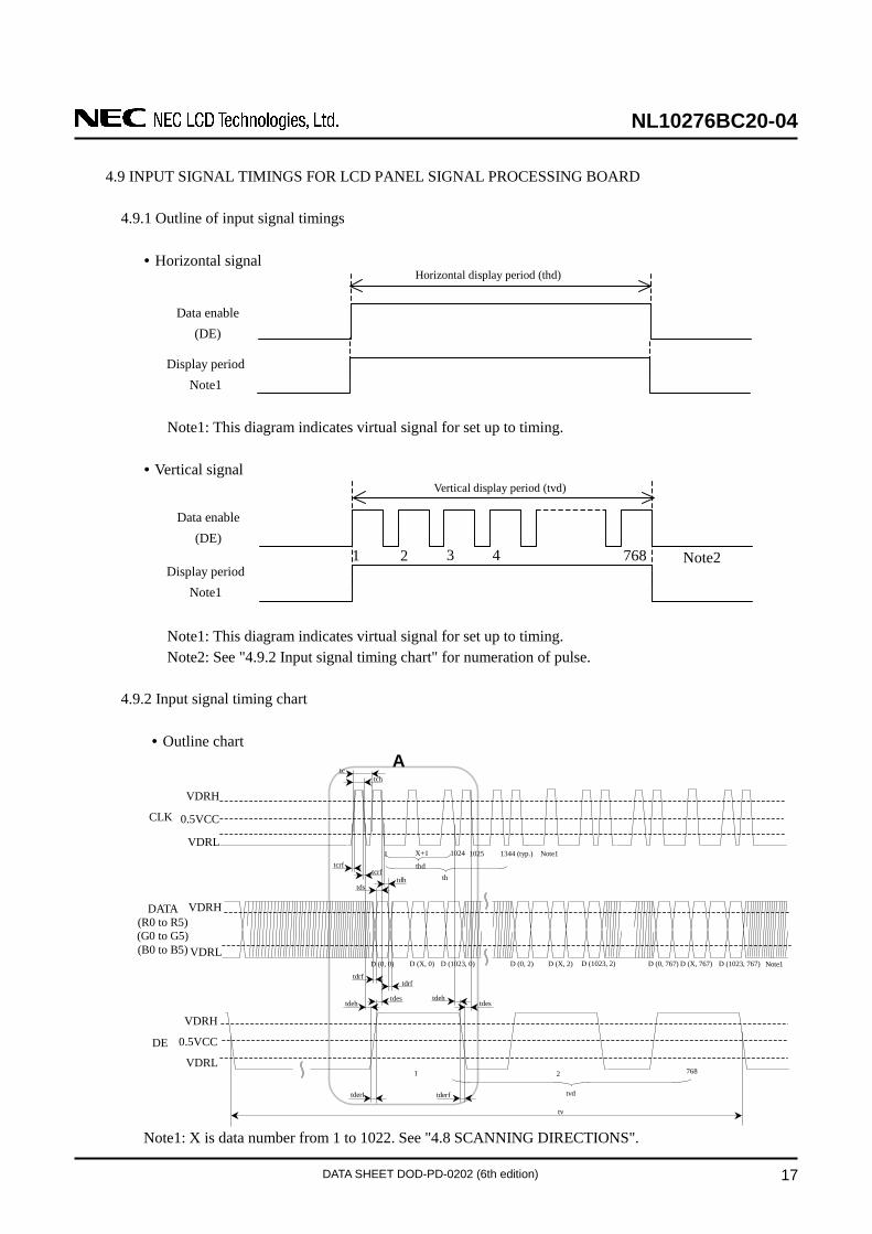
4.9 INPUT SIGNAL TIMINGS FOR LCD PANEL SIGNAL PROCESSING BOARD
4.9.1 Outline of input signal timings
• Horizontal signal
Note1: This diagram indicates virtual signal for set up to timing.
• Vertical signal
Note1: This diagram indicates virtual signal for set up to timing.Note2: See "4.9.2 Input signal timing chart" for numeration of pulse.
4.9.2 Input signal timing chart
• Outline chart
Note1: X is data number from 1 to 1022. See "4.8 SCANNING DIRECTIONS".
Display periodNote1
Horizontal display period (thd)
Data enable(DE)
Vertical display period (tvd)
1 2 3 4 768Display period
Note1
Data enable(DE)
Note2
DE
VDRH
0.5VCC
VDRL
CLK
VDRH
VDRL
DATA(R0 to R5)(G0 to G5)(B0 to B5)
tdestdeh
tdrftdrf
tdstdh
tcrftcrf
tchtc
1024
D (0, 0) D (1023, 0)
7681
D (X, 0)
thd
tvd
A
X+1
tdes
tderf tderf
Note11
2
D (X, 2)D (0, 2) D (1023, 2)
1344 (typ.)
tdeh
1025
D (X, 767)D (0, 767) D (1023, 767)
VDRH
0.5VCC
VDRL
tv
th
Note1
NL10276BC20-04
DATA SHEET DOD-PD-0202 (6th edition) 18
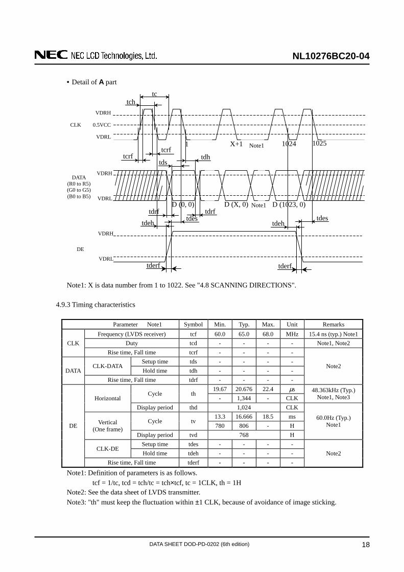
• Detail of A part
Note1: X is data number from 1 to 1022. See "4.8 SCANNING DIRECTIONS".
4.9.3 Timing characteristics
Parameter Note1 Symbol Min. Typ. Max. Unit RemarksFrequency (LVDS receiver) tcf 60.0 65.0 68.0 MHz 15.4 ns (typ.) Note1
Duty tcd - - - - Note1, Note2CLKRise time, Fall time tcrf - - - -
Setup time tds - - - -CLK-DATA
Hold time tdh - - - -DATARise time, Fall time tdrf - - - -
Note2
19.67 20.676 22.4 µsCycle th
- 1,344 - CLK48.363kHz (Typ.)
Note1, Note3HorizontalDisplay period thd 1,024 CLK
13.3 16.666 18.5 msCycle tv
780 806 - HVertical(One frame)
Display period tvd 768 H
60.0Hz (Typ.)Note1
Setup time tdes - - - -CLK-DE
Hold time tdeh - - - -
DE
Rise time, Fall time tderf - - - -Note2
Note1: Definition of parameters is as follows.tcf = 1/tc, tcd = tch/tc = tch×tcf, tc = 1CLK, th = 1H
Note2: See the data sheet of LVDS transmitter.Note3: "th" must keep the fluctuation within ±1 CLK, because of avoidance of image sticking.
VDRH
0.5VCC
VDRL
CLK
tdstdh
tdrftdrf
tc
tcrf
tderf
VDRH
VDRL
DATA(R0 to R5)(G0 to G5)(B0 to B5)
DE
tch
tcrf
tdeh tdes
tderf
tdehtdes
VDRH
VDRL
D (0, 0) D (X, 0) D (1023, 0)
1 X+1 1024 1025Note1
Note1
NL10276BC20-04
DATA SHEET DOD-PD-0202 (6th edition) 19
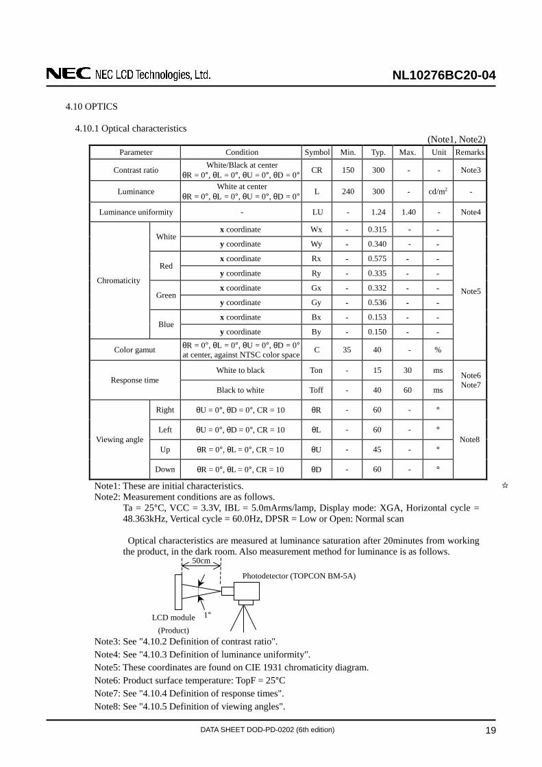
4.10 OPTICS
4.10.1 Optical characteristics(Note1, Note2)
Parameter Condition Symbol Min. Typ. Max. Unit Remarks
Contrast ratio White/Black at centerθR = 0°, θL = 0°, θU = 0°, θD = 0° CR 150 300 - - Note3
Luminance White at centerθR = 0°, θL = 0°, θU = 0°, θD = 0° L 240 300 - cd/m2 -
Luminance uniformity - LU - 1.24 1.40 - Note4
x coordinate Wx - 0.315 - -White
y coordinate Wy - 0.340 - -
x coordinate Rx - 0.575 - -Red
y coordinate Ry - 0.335 - -
x coordinate Gx - 0.332 - -Green
y coordinate Gy - 0.536 - -
x coordinate Bx - 0.153 - -
Chromaticity
Bluey coordinate By - 0.150 - -
Color gamut θR = 0°, θL = 0°, θU = 0°, θD = 0°at center, against NTSC color space C 35 40 - %
Note5
White to black Ton - 15 30 msResponse time
Black to white Toff - 40 60 ms
Note6Note7
Right θU = 0°, θD = 0°, CR = 10 θR - 60 - °
Left θU = 0°, θD = 0°, CR = 10 θL - 60 - °
Up θR = 0°, θL = 0°, CR = 10 θU - 45 - °Viewing angle
Down θR = 0°, θL = 0°, CR = 10 θD - 60 - °
Note8
Note1: These are initial characteristics.Note2: Measurement conditions are as follows.
Ta = 25°C, VCC = 3.3V, IBL = 5.0mArms/lamp, Display mode: XGA, Horizontal cycle =48.363kHz, Vertical cycle = 60.0Hz, DPSR = Low or Open: Normal scan
Optical characteristics are measured at luminance saturation after 20minutes from workingthe product, in the dark room. Also measurement method for luminance is as follows.
Note3: See "4.10.2 Definition of contrast ratio".Note4: See "4.10.3 Definition of luminance uniformity".Note5: These coordinates are found on CIE 1931 chromaticity diagram.Note6: Product surface temperature: TopF = 25°CNote7: See "4.10.4 Definition of response times".Note8: See "4.10.5 Definition of viewing angles".
1°
Photodetector (TOPCON BM-5A)
LCD module(Product)
50cm
NL10276BC20-04
DATA SHEET DOD-PD-0202 (6th edition) 20
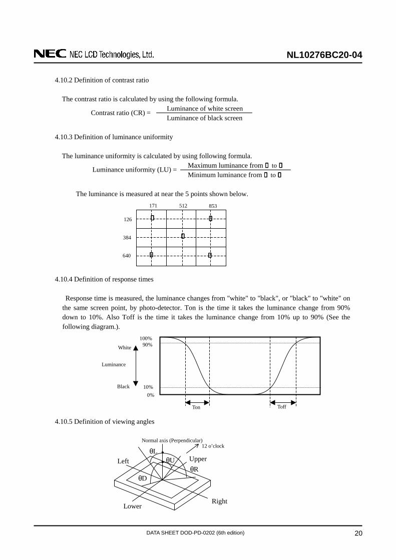
4.10.2 Definition of contrast ratio
The contrast ratio is calculated by using the following formula.Luminance of white screenLuminance of black screen
4.10.3 Definition of luminance uniformity
The luminance uniformity is calculated by using following formula.Maximum luminance from ①①①① to ⑤⑤⑤⑤Minimum luminance from ①①①① to ⑤⑤⑤⑤
The luminance is measured at near the 5 points shown below.
4.10.4 Definition of response times
Response time is measured, the luminance changes from "white" to "black", or "black" to "white" onthe same screen point, by photo-detector. Ton is the time it takes the luminance change from 90%down to 10%. Also Toff is the time it takes the luminance change from 10% up to 90% (See thefollowing diagram.).
4.10.5 Definition of viewing angles
①①①① ②②②②
③③③③
④④④④ ⑤⑤⑤⑤
171 512 853
126
384
640
Contrast ratio (CR) =
Luminance uniformity (LU) =
Left Upper
Lower
Normal axis (Perpendicular)
θU
θDθR
θL12 o’clock
Right
100% 90%
10% 0%
Ton Toff
Luminance
White
Black
NL10276BC20-04
DATA SHEET DOD-PD-0202 (6th edition) 21
5. RELIABILITY TESTS
Test item Condition Judgement
High temperature and humidity(Operation)
① 55 ± 2°C, RH = 85%, 240hours② Display data is black.
High temperature(Operation)
① 60 ± 2°C, 240hours② Display data is black.
Heat cycle(Operation)
① 0 ± 3°C…1hour60 ± 3°C…1hour
② 50cycles, 4hours/cycle③ Display data is black.
Thermal shock(Non operation)
① -20 ± 3°C…30minutes70 ± 3°C…30minutes
② 100cycles, 1hour/cycle③ Temperature transition time is within 5
minutes.
ESD(Operation)
① 150pF, 150Ω, ±10kV② 9 places on a panel surface Note2③ 10 times each places at 1 sec interval
Dust(Operation)
① Sample dust: No. 15 (by JIS-Z8901)② 15 seconds stir③ 8 times repeat at 1 hour interval
No display malfunctions Note1
Vibration(Non operation)
① 5 to 100Hz, 11.76m/s2
② 1 minute/cycle③ X, Y, Z direction④ 120 times each directions
Mechanical shock(Non operation)
① 539m/ s2, 11ms② ±X, ±Y, ±Z direction③ 5 times each directions
No display malfunctionsNo physical damages
Note1
Note1: Display and appearance are checked under environmental conditions equivalent to theinspection conditions of defect criteria.
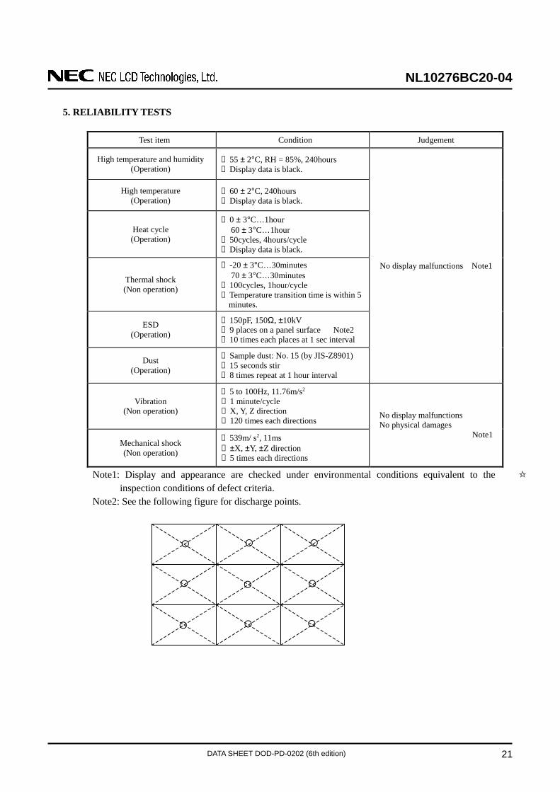
Note2: See the following figure for discharge points.
NL10276BC20-04
DATA SHEET DOD-PD-0202 (6th edition) 22
6. PRECAUTIONS
6.1 MEANING OF CAUTION SIGNS
The following caution signs have very important meaning. Be sure to read "6.2 CAUTIONS" and"6.3 ATTENTIONS", after understanding this contents!
!This sign has the meaning that customer will be injured by himself or the product will
sustain a damage, if customer has wrong operations.
This sign has the meaning that customer will get an electrical shock, if customer haswrong operations.
This sign has the meaning that customer will be injured by himself, if customer haswrong operations.
6.2 CAUTIONS
∗∗∗∗ Do not touch the working backlight. Customer will be in danger of an electric shock.
∗∗∗∗ Do not touch the working backlight. Customer will be in danger of burn injury.∗∗∗∗ Do not shock and press the LCD panel and the backlight! There is a danger of breaking,
because they are made of glass. (Shock: To be not greater 539m/s2 and to be not greater11ms, Pressure: To be not greater 19.6 N)
6.3 ATTENTIONS !
6.3.1 Handling of the product
① Take hold of both ends without touch the circuit board cover when customer pulls out products(LCD modules) from inner packing box. If customer touches it, products may be broken down orout of adjustment, because of stress to mounting parts.
② Do not hook cables nor pull connection cables such as lamp cable and so on, for fear of damage.③ If customer puts down the product temporarily, the product puts on flat subsoil as a display side
turns down.④ Take the measures of electrostatic discharge such as earth band, ionic shower and so on, when
customer deals with the product, because products may be damaged by electrostatic.⑤ The torque for mounting screws must never exceed 0.294N⋅m. Higher torque values might result in
distortion of the bezel.⑥ The product must be installed using mounting holes without undue stress such as bends or twist
(See outline drawings). And do not add undue stress to any portion (such as bezel flat area) exceptmounting hole portion.Bends or twist described above and undue stress to any portion except mounting hole portion maycause display un-uniformity.
NL10276BC20-04
DATA SHEET DOD-PD-0202 (6th edition) 23
⑦ Do not press or rub on the sensitive display surface. If customer clean on the panel surface, NECrecommends using the cloth with ethanolic liquid such as screen cleaner for LCD.
⑧ Do not push-pull the interface connectors while the product is working, because wrong powersequence may break down the product.
⑨ Do not bend or unbend the lamp cable at the near part of the lamp holding rubber, to avoid thedamage for high voltage side of the lamp. This damage may cause a lamp breaking and abnormaloperation of high voltage circuit.
6.3.2 Environment
① Do not operate or store in high temperature, high humidity, dewdrop atmosphere or corrosive gases.Keep the product in antistatic pouch in room temperature, because of avoidance for dusts andsunlight, if customer stores the product.
② In order to prevent dew condensation occurring by temperature difference, the product packing boxmust be opened after leave under the environment of an unpacking room temperature enough.Because a situation of dew condensation occurring is changed by the environmental temperatureand humidity, evaluate the leaving time sufficiently. (Recommendation leaving time: 6 hour or morewith packing state)
③ Do not operate in high magnetic field. Circuit boards may be broken down by it.④ This product is not designed as radiation hardened.⑤ Use an original protection sheet on the product surface (polarizer). Adhesive type protection sheet
should be avoided, because it may change color or properties of the polarizer.
6.3.3 Characteristics
The following items are neither defects nor failures.
① Response time, luminance and color may be changed by ambient temperature.② The LCD may be seemed luminance non-uniformity, flicker, vertical seam or small spot by display
patterns.③ Optical characteristics (e.g. luminance, display uniformity, etc.) gradually is going to change
depending on operating time, and especially low temperature, because the LCD has cold cathodefluorescent lamps.
④ Do not display the fixed pattern for a long time because it may cause image sticking. Use a screensaver, if the fixed pattern is displayed on the screen.
⑤ The display color may be changed by viewing angle because of the use of condenser sheet in thebacklight.
⑥ Optical characteristics may be changed by input signal timings.⑦ The interference noise of input signal frequency for this product's signal processing board and
luminance control frequency of customer's backlight inverter may appear on a display. Set upluminance control frequency of backlight inverter so that the interference noise does not appear.
6.3.4 Other
① All GND and VCC terminals should be used without a non-connected line.② Do not disassemble a product or adjust volume without permission of NEC.③ See "REPLACEMENT MANUAL FOR LAMP HOLDER SET", if customer would like to replace
backlight lamps.④ Pay attention not to insert waste materials inside of products, if customer uses screwnails.⑤ Pack the product with original shipping package, because of avoidance of some damages during
transportation, when customer returns it to NEC for repair and so on.
NL10276BC20-04
DATA SHEET DOD-PD-0202 (6th edition) 24
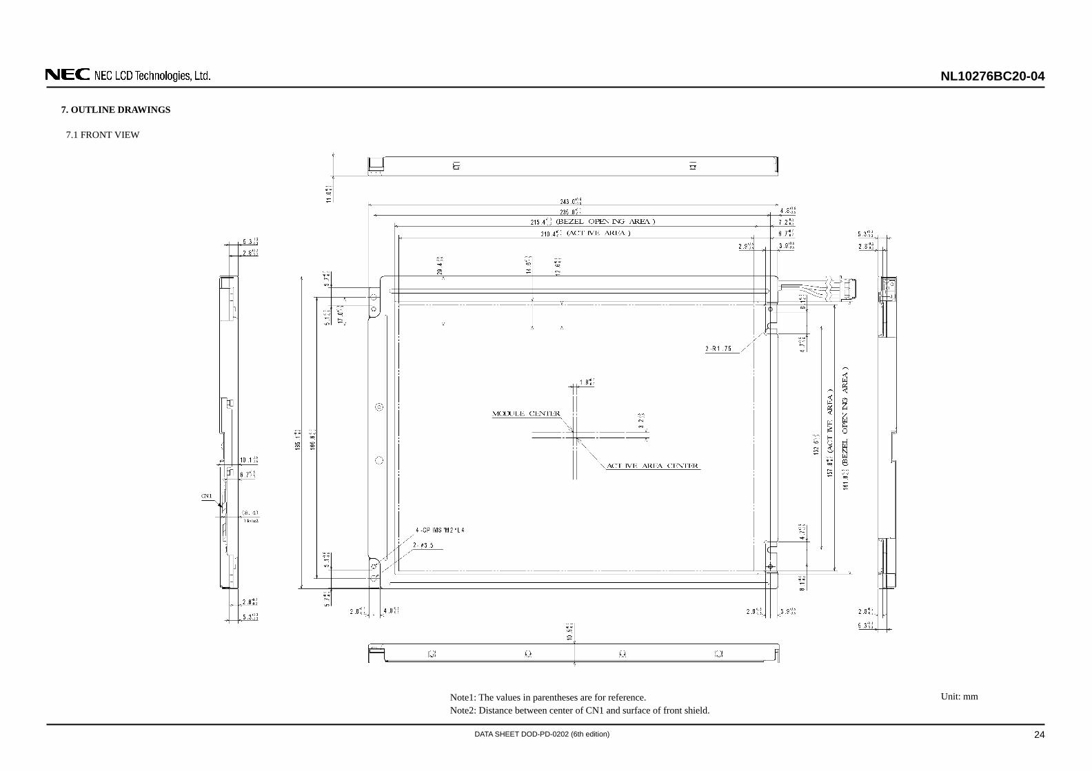
7. OUTLINE DRAWINGS
7.1 FRONT VIEW
Unit: mmNote1: The values in parentheses are for reference.Note2: Distance between center of CN1 and surface of front shield.
NL10276BC20-04
DATA SHEET DOD-PD-0202 (6th edition) 25
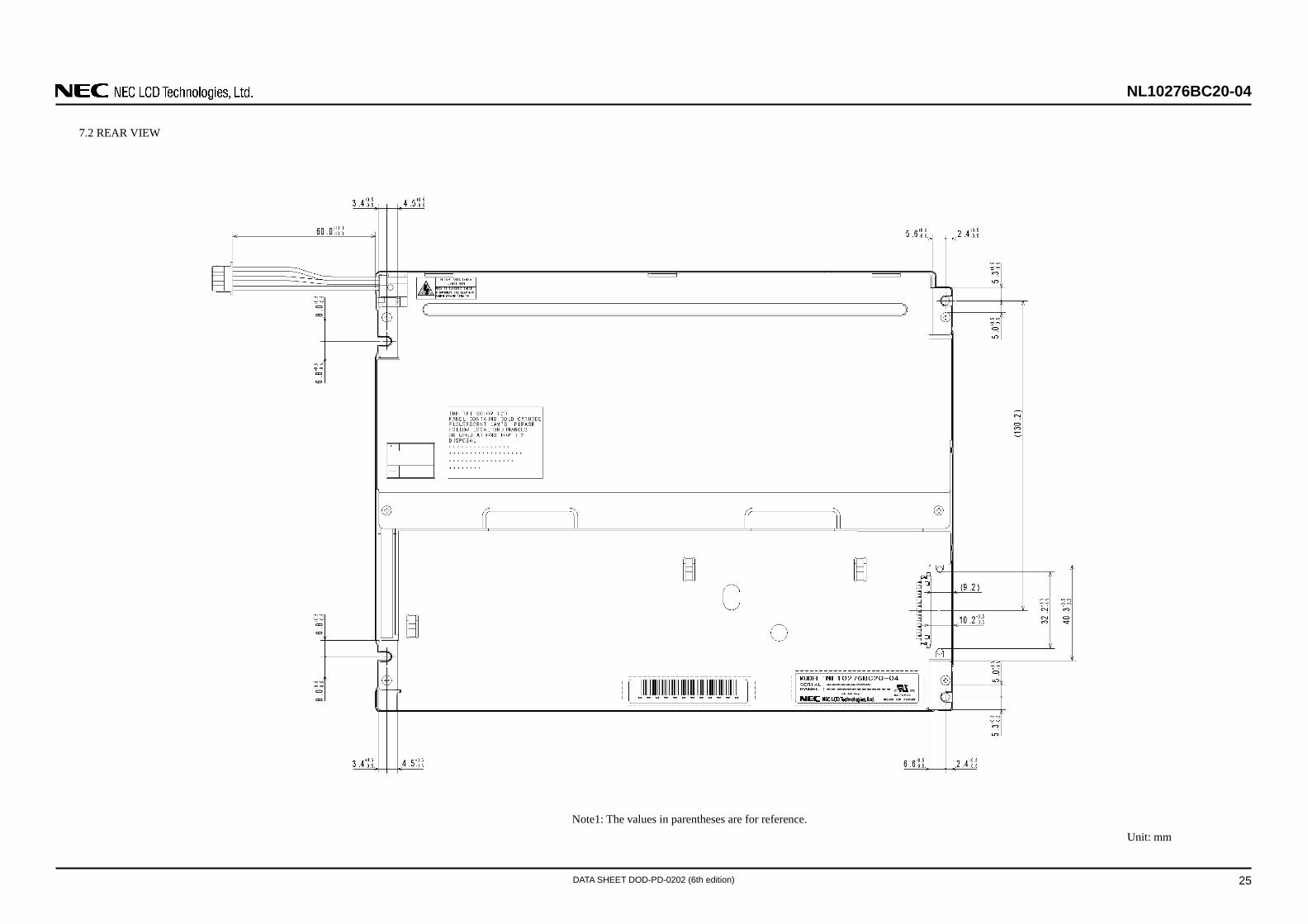
7.2 REAR VIEW
Unit: mmNote1: The values in parentheses are for reference.