Embed Size (px)
Citation preview

AD-A239 767
ESD-TR-91-215 MTR-1 1119
Dose Rate and Total Dose Radiation Testing of theTexas Instruments TMS320C30 32-Bit Floating Point
Digital Signal Processor
By
P. F. Siy -
J. T. CarterL. R. D'Addario ,
D. A. Loeber ,
August 1991
Prepared for
Deputy Program DirectorStrategic C3 Systems
Electronic Systems DivisionAir Force Systems Command
United States Air Force
Hanscom Air Force Base, Massachusetts
91-08906~ II I rl llll 11111 ~ 1111 ~l iilII Project No. 6520
Prepared by
The MITRE CorporationSApproed for public release. Bedford, Massachusettsdistribution unlimited.
Contract No. F19628-89-C-0001
1,J
When U.S. Government drawings, specificationsor other data are used for any purpose otherthan a definitely related government procure-ment operation, the government thereby incursno responsibility nor any obligation whatsoever;and the fact that the government may have for-mulated, furnished, or in any way supplied thesaid drawings, specifications, or other data isnot to be regarded by implication or otherwiseas in an% manner licensing the holder or anyother person or conveying any' rights or permis-sion to manufacture, use, or sell any patentedinvention that may in any way be relatedthereto.
Do not return this cop. Retain or destroy.
REVIEW AND APPROVAL
This technical report has been reviewed and is approved for publication.
MICHAEL J. GOCI, LT COL, USAFAVR Program Manager
FOR THE COMMANDER
RAYMOND J. ALBERTDeputy Program Director,
Strategic C3 Systems

1 Form ApprovedREPORT DOCUMENTATION PAGE O MB No 0704-0188ru,,eo-,t n4 ou'de, 0' this concnwn 0* -cIatcn s ntin-a-e to &,etagii hour o- esoo~se nca,hc t"P r'me tol,e - h i nstcticni, se ~ e, it = data so,."ee
qatt'erin anc maintaining th'e data needed. and con~oieiinq and e -P-ng tt'e cosctcn of nfcrmariom Sena comments reoardinq this ourden es Iimle n .~ :v'e, asoe'! o. ?ncoliection Ct f - onatior inciuadng ts.gaiiitcor reac'inj N OeSm~~ tO Wa~hfMlfqOn 'feadaaa!C'% Servie% C,.ecto,ate fc Io~'mat-oh 0Oie,at-ons and RDocr1s '2 15 jeffetaonDa~,H? v.t 2.A~ntni 22202-4C an tC~office~ -:I, laagm-t and Budqe- PaoeriOi Renau-tio' Proent (0710.OtBS) vva~i,,ntcr DC 2S.
1. AGENCY USE ONLY (Leave Wlank) 12. REPORT DATE 3.REPORT TYPE AND DATES COVERED
IAugust 1991 Final _____________
4. TITLE AND SUBTITLE 5. FUNDING NUMBERS
Dose Rate and Total Dose Radiation Testing of the TexasInstruments TMS32OC30 32-Bit Floating Point Digital F19628-89-C-0001Signal Processor 6520
6. AUTHOR(S) Siy, Peter F.Carter, Jeffrey T.D'Addario, Lawrence R.Loeber, David A. ____________
7. PERFORMING ORGANIZATION NAME(S) AND ADDRESS(ES) B. PERFORMING ORGANIZATION
The MITRE Corporation REPORT NUMBER
Burlington Road MTR- 11119Bedford, MA 01730
9. SPONSORING / MONITORING AGENCY NAME(S) AND ADDRESS(ES) 10. SPONSORING I MONITORING
Deputy Program Director, Strategic C3 Systems (ESD/SZB) AGENCY REPORT NUMBER
Electronic Systems Division, AFSC ESD-TR-91-215Hanscom AFB, MA 01731-5000
11. SUPPLEMENTARY NOTES
12a. DISTRIBUTION / AVAILABILITY STATEMENT 12b. DISTRIBUTION CODE
Approved for public release; distribution unlimited.
13. ABSTRACT (Maximum 200 words)
The MITRE Corporation has performed in-flux radiation testing of the TexasInstruments TMS320C30 32-bit floating point digital signal processor in bothtotal dose and dose rate radiation environments. This test effort has provided datarelating to the applicability of the TMS32OC30 in systems with total dose and/ordose rate survivability requirements. In order to accomplish these tests, The!=IRE Corporation developed custom hardware and software for in-flux radiationtesting. This paper summarizes the effort by providing an over-view of theTMS320C30, MITRE's test methodology, test facilities, statistical analysis, andfull coverage of the test results.
14. SUBJECT TERMS 15. NUMBER OF PAGES
Digital Signal Processing (DSP) Radiation Testing 33Dose Rate Radiation Test TMS320C30 DSP 16. PRICE CODERadiation Characterization Total Dose Radiation Test __________
17. SECURITY CLASSIFICATION 18. SECURITY CLASSIFICATION 19. SECURITY CLASSIFICATION 20. LIMITATION OF ABSTRACTOF REPORT I OF THIS PAGE I OF ABSTRACT
Unclassified Unclassified Unclassified A
NSN 7540-01-280-5500 Standard Form 298 (Rev 2-89)P~emcrbe bv ANSI SICd Z39-18298 102

ACKNOWLEDGEMENTS
This document has been prepared by The MITRE Corporation under ProjectNo. 6520, Contract No. F19628-89-C-0001. The contract is sponsored by the ElectronicSystems Division, Air Force Systems Command, United States Air Force, Hanscom AirForce Base, Massachusetts 01731-5000.
The authors would like to thank Mr. Jim Larimer, Texas Instruments Military ProductsDepartment, Semiconductor Group, Midland, Texas for his support and encouragementthroughout this project.
iii

TABLE OF CONTENTS
SECTION PAGE
1 Introduction 1
2 Overview of the TMS320C30 DSP 3
3 Test Bed Description 5
4 Test Overview 7
4.1 Total Dose Testing 74.2 Dose Rate Testing 7
4.2.1 Upset 84.2.2 Latch-Up 8
4.3 Dosimetry 8
5 Data Analysis Techniques 9
5.1 Calculation of the Sample Mean and Standard Deviation 95.2 Calculation of the Adjusted Mean 95.3 Calculation of the Statistical Failure Level 105.4 Calculation of the Probability of Survival 12
6 Test Results 15
6.1 Total Dose Test Results 15
6.2 Dose Rate Test Results 176.2.1 Prompt Environment 176.2.2 Delayed Environment 18
6.3 Discussion !9
7 Conclusion 21
List of References 23
Glossary 25
v

LIST OF FIGURES
FIGURE PAGE
1 Basic TMS320C30 Block Diagram 3
2 TMS320C30 Radiation Test Fixture 5
3 MITRE-Developed Test Bed for TMS320C30 Radiation Testing 6
4 Total Dose Probability of Survival 16
5 Average Device Current versus Total Accumulated Dose 16
6 Prompt Dose Rate Probability of No Upset 18
7 Delayed Dose Rate Probability of No Upset 20
LIST OF TABLES
TABLE PAGE
1 Summary of EPIC-IA and EPIC-1Z Process Differences 4
2 Tolerance Factors for the Xa and SFL Calculations for Various Sample Sizes 11
3 KTL Values for Ps Interpolation for Various Sample Sizes (n) 13
4 Total Dose Test Results 15
5 Prompt Dose Rate Upset Threshold Results (Narrow Pulse) 17
6 Prompt Dose Rate Latch-Up Results (Narrow Pulse) 17
7 Delayed Dose Rate Upset Threshold Results (Wide Pulse) 19
8 Delayed Dose Rate Latch-Up Results (Wide Pulse) 19
vi
SECTION 1
INTRODUCTION
This paper describes a test program initiated by The MITRE Corporation to characterizethe Texas Instruments (TI) TMS320C30 32-bit floating point digital signal processor (DSP)in both dose rate and total dose radiation environments. This device is applicable to a widerange of signal processing needs including communications, radar, sonar, image processing,navigation, and missile guidance. The processor provides 32-bit floating point signalprocessing capabilities via a single-chip architecture. In addition, it is the only DSP deviceto offer a validated Ada compiler for high-level language development as required by manyDOD programs. As such, this state-of-the-art device will be a key component in many systemsincluding those with radiation survivability requirements.
The growth of digital signal processing has been fueled by the advent of single-chip DSPscapable of performing fast (single-cycle) multiply and accumulate operations, the staple ofall signal processing algorithms. These application-specific microprocessors have evolvedfrom 8- and 16-bit fixed point devices to the current 32-bit floating point capabilities. Thesecapabilities naturally lend themselves to many communications programs as well as otherinterests including those with radiation hardening requirements. Recognizing the importance ofthis capability, The MITRE Corporation has characterized this device in the total dose and doserate radiation environments. Texas Instruments provided 20 devices as well as sophisticateddevelopment tools used by MITRE staff to develop a TMS32OC30 radiation test bed.
MITRE's test of the TMS320C30 resulted in failures between 4- and 5-K rads (Si) in thetotal dose environment with a statistical failure level (99-percent probability of survival with90-percent confidence) of approximately 3-K rads (Si). In the prompt dose rate environmentusing a 20-30-nanosecond (ns) pulse, the device failed in the area of 1 x 10⁸ rads (Si) persecond with a 99/90 failure level of approximately 7 x 10⁷ rads (Si) per second. For thedelayed dose rate environment using a 1-microsecond (pts) pulse, the device failed in the areaof 5 x 10⁷ rads (Si) per second with a 99/90 failure level of approximately 3.2 x 10⁷ rads (Si)per second. We observed latch-up in both environments at room temperature, at approximately1 x 109 rads (Si) per second in the prompt environment and at approximately I x 108 rads (Si)per second in the delayed environment.
This paper will provide an overview of the TMS320C30 and its fabrication and willdescribe the test bed developed by MITRE. An overview of the tests and the formulation ofapplicable statistics will then be provided. Finally, we will provide the results of all tests andrelevant discussion.

SECTION 2
OVERVIEW OF THE TMS320C30 DSP
The TMS320C30 is a complementary metal-oxide semiconductor (CMOS) integratedcircuit with TTL-compatible inputs and outputs [1]. The DSP has a single-cycle instructionexecution time of 60 ns. The processor, fabricated in 1.0-micron (gim) technology, consists ofapproxi- mately 700,000 transistors. The version supplied is housed in a 180-pin ceramic pingrid array (PGA) package. Relevant to radiation characterization, the TMS320C30 is adynamic device -- it relies on inherent internal capacitance for logic level storage and,therefore, has a minimum operating frequency.
One special feature is its true in-circuit emulation capability. The device is equipped witha modular port scan device, or scan path. This feature allows the connection of an XDS500emulator, which, unlike previous generation microprocessors, does not require the deviceto be removed from its target and replaced with an emulator pod to perform softwaredevelopment and test via device emulation. A block diagram of the TMS320C30 DSP isprovided in figure 1.
Program RAM RAM ROMCache Block 0 Block I Block 0
Primary Bus x(16M Address Space) (8K Address Space)
RESET CPU DMA
I ( --. , regr r/ Address Seia Port -lACK Floating Point Fig G ne Ors
XF(1-O) - C Multplier ALU C I S1o
C/ n 8 Extended Precision rXl I tRegistersX2/CLKlN r
VCC(7-0) -- 0 o Address Address Timer 00GeneratorO Generator1
VBBP --- s- e ,u Timrer 1 '--
SUBS -so r 8 Auxiliary Registers
EMU3, --- 12 Control RegistersH3<P..
Figure 1. Basic TMS320C30 Block Diagram
3
The TMS320C30 has a 24-bit address space, which allows it to address 16 million 32-bitwords of external memory. In addition, it contains several areas of on-chip memory includinga 4-K x 32-bit on-chip ROM block, two 1-K x 32-bit on-chip RAM blocks, and a 64- x 32-bitinstruction cache. It contains eight extended precision registers and eight auxiliary registers.Its on-chip peripherals include a direct memory access (DMA) controller, serial ports, andtimers.
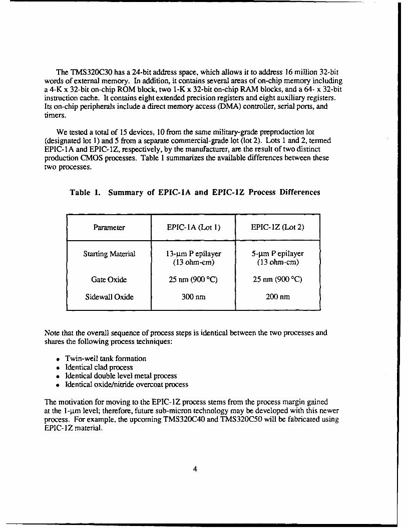
We tested a total of 15 devices, 10 from the same military-grade preproduction lot(designated lot 1) and 5 from a separate commercial-grade lot (lot 2). Lots 1 and 2, termedEPIC-lA and EPIC-1Z, respectively, by the manufacturer, are the result of two distinctproduction CMOS processes. Table 1 summarizes the available differences between thesetwo processes.
Table 1. Summary of EPIC-1A and EPIC-1Z Process Differences
Parameter EPIC-lA (Lot 1) EPIC-1Z (Lot 2)
Starting Material 13-pgm P epilayer 5-g.m P epilayer
(13 ohm-cm) (13 ohm-cm)
Gate Oxide 25 nm (900 'C) 25 nm (900 'C)
Sidewall Oxide 300 nm 200 nm
Note that the overall sequence of process steps is identical between the two processes andshares the following process techniques:
" Twin-well tank formation* Identical clad process" Identical double level metal process" Identical oxide/nitride overcoat process
The motivation for moving to the EPIC-1Z process stems from the process margin gainedat the 1-p.m level; therefore, future sub-micron technology may be developed with this newerprocess. For example, the upcoming TMS320C40 and TMS320C50 will be fabricated usingEPIC- I Z material.
4

SECTION 3
TEST BED DESCRIPTION
While there continues to be a growing need for radiation data for increasingly higherspeed microprocessors, testing of such critical devices continues to become increasingly moredifficult. Before developing test fixtures to accomplish this testing, a literature search of testmethods used for other microprocessors revealed a diversity of methods. We examined testsfor such devices as the Intel 8080 [2], 8085 [2,3,4], 8086 [5,6], 80186 [7], 80286 [7], and80386 [8]; the Inmos Transputer [9]; the Motorola 6800 [2,3], 68000 [10], and 68020 [11];and the Zilog Z8OA [6,12,13,14] and Z8002A [10,12]. After reviewing the cited tests of thevarious microprocessors listed, we discussed the various methodologies with authorities in thefield [15,16,17]. Our investigation led to our test methodology for this device. We performedfull in-flux testing while operating the device at full speed. We chose to perform in-flux testsin an effort to provide an accurate characterization of the device's radiation performance.While we are aware that radiation susceptibility may be clock-rate dependent, we operated thedevice at full speed (16 MHz) since this is a DSP's normal operational regime. Our testing canbe classified as that of external control -- we controlled/monitored the device under test via Ti'sXDS 1000 development environment. While we readily employed the XDS 1000, it did notprovide us the required platform for any radiation environment -- a stand-alone TMS320C30-based card with (external) communications capabilities. For this, we designed and assembleda stand-alone card. Our test fixture consists of a single TMS320C30 with minimal supportcircuitry, which is shielded during testing, as shown in figure 2.
Reset -P~an
Cl I TMS320C30 Header
Exposed Primary Serial
Side Data
Shielded
Circuitr Line Drivers/ -
Osilt R a IRe ce ive rs ITest FixtureM 0 Status
Figure 2. TMS320C30 Radiation Test Fixture
5

We developed our own custom assembly language programs to test the device. Theseprograms provide comparable completeness to other methods we reviewed -- they test allfunctional components of the device, use much of the instruction set, and are robust inreporting errors in the wake of radiation effects. These programs execute on the deviceunder test and output test status via one of two on-chip serial ports. Results are passedto a second TMS320C30, part of the XDS 1000 development environment, operating ina PC-AT-compatible Zenith Z-248 computer. This second DSP, which operates outsideof the radiation environment, provides test results to the host PC's controlling 80286microprocessor. Results are continuously provided/updated on the PC's display. Testsaccomplished include:
* CPU register file" On-chip memory* On-chip cache* On-chip peripherals" Multiplier, arithmetic logic unit (ALU), auxiliary register arithmetic unit (ARAU)
I TMS32OC30serial ScanData PathtTest I ,,
Fixture, I ;. ;' " .. iApiiao TMS320C30 80286
Protoboard on Emulator (8 MHz)
Radiation IEnvironment ( Z
, --Isu:I, .,,TI DS0, ,Environment
Figure 3. MITRE-Developed Test Bed for TMS320C30 Radiation Testing
6
SECTION 4
TEST OVERVIEW
Testing of the TMS320C30 determined the total dose failure level, dose rate upsetthreshold level, and dose rate latch-up threshold level. The testing was performed at theRome Air Development Center (RADC) radiation facility located at Hanscom Air ForceBase in Bedford, MA. The following subsections provide further details of the testprocedures and facilities.
4.1 TOTAL DOSE TESTING
The total dose testing of the TMS320C30 was conducted in accordance with the require-ments of MIL-STD-883C, method 1019.3 [18]. The exception was that testing was performedat a dose rate of approximately 575 rads (Si) per minute. Testing continued until each devicehad a functional failure. The testing was performed on a sample size of 10 devices from theEPIC-lA process and 3 devices from the EPIC-1Z process. In addition to the devices beingtested, sufficient unirradiated controls were used to ensure proper operation of the test fixture.The testing of the TMS320C30 was conducted in-flux (i.e., functional testing was performedduring the radiation exposure). Upon detecting a functional failure, the test fixture recorded thetime the failure occurred. In addition, current measurements were taken to characterize devicecurrent (Icc) versus total accumulated dose.
The total dose facility uses a Cobalt-60 (Co-60) source. The Co-60 cell is a dry room(10' x 10' x 10') with the source mounted on an elevator assembly positioned near the middleof the room. The strength of the source is approximately 27,000 curies. The radiationexposure rate is determined by the distance of the exposed specimens from the Co-60 source.
4.2 DOSE RATE TESTING
We tested the TMS320C30 to determine the dose rate threshold for upset of the device andto demonstrate the dose-rate-induced latch-up immunity of the device. Testing was performedusing both a 20-30-ns full width half maximum (FWHM) pulse and a 1-1as FWHM pulsewidth. The dose rate testing was performed using both the flash X-ray machine and theLINAC. The flash X-ray facility contains a Pulserad 314 machine manufactured by PhysicsInternational Company. The maximum dose rate achievable is 1.6 x 10¹⁰ rads (Si) per secondwith a 20-ns FWHM pulse width. The dose rate that the exposed specimen receives isdetermined by the distance from the machine's output port. The LINAC facility contains an18-MeV machine manufactured by Applied Radiation Corporation. The LINAC operates in theelectron beam mode for this experiment. The maximum dose rate achievable is 1.3 x 10¹² rads(Si) per second with a 20-ns FWHM pulse width and 2.6 x 10¹⁰ rads (Si) per second with a1-4ts FWHM pulse width.
7
4.2.1 Upset
The dose rate upset testing of the TMS320C30 device was in accordance with therequirements of MIL-STD-883C, method 1021.1 [191. The device was continuouslyfunctionally tested throughout the dose rate exposure. The test fixture monitored the internalregisters and memory locations of the device while being exposed to subsequently higher doserates. An upset was defined as any change of state in either the internal registers or the internalmemory locations.
4.2.2 Latch-Up
The dose rate latch-up testing of the TMS320C30 device was in accordance with therequirements of MIL-STD-883C, method 1020 [20], with the exception that all testing wasperformed at room temperature. The test fixture power supply current and functionality of thedevice were monitored. The device was exposed to subsequently higher dose rates until alatch-up condition occurred. Latch-up was indicated by a current draw significantly greaterthan nominal, excessive device heating and partial to complete loss of functionality.
4.3 DOSIMETRY
The test facility provided the dosimetry necessary to establish an accurate measurement ofthe radiation dose received by the TMS320C30 test specimens. These dosimetry proceduresare traceable to the National Institute of Standards and Technology (NIST). The dosimetry forthe total dose experiment was provided by a Victoreen Model 500 Precision Medical PhysicsElectrometer. This instrument measures the dose rate of the radiation exposure. Calibration ofthe dosimetry system is accomplished using thermoluminescent dosimeters (TLDs). The doserate multiplied by the time of the exposure will yield the total dose accumulated in the testspecimens.
The dosimetry for the dose rate experiments was provided by a UM4001 PIN diode.The PIN diode is biased with +100 volts and terminated into a 50-ohm load at an oscilloscopeinput. The photocurrent of the diode is proportional to the dose rate exposure. The PIN dioderesponse versus the dose rate is 1.1 x 10⁸ rads (Si) per second per volt. This calibration factoris determined using TLDs.
8

SECTION 5
DATA ANALYSIS TECHNIQUES
We performed a statistical analysis of the test results assuming that the radiation responseof the devices followed a lognormal probability distribution. This assumption has beenaccepted by the nuclear hardening community [21]. (The adoption of this assumption allowsthe inference of population characteristics from a small sample of data.) Since the calculationsmust be performed in log space, the real failure levels acquired from the testing are firstconverted to their equivalent natural logs. The sample mean and standard deviation can thenbe calculated in log space. These values are then used to determine the adjusted mean failurelevel, statistical failure level (SFL), and probability of survival (Ps) for the TMS320C30. Afterthese calculations are complete, the results are converted to their equivalent real values forreporting in section 6.
5.1 CALCULATION OF THE SAMPLE MEAN AND STANDARDDEVIATION
We reduced the radiation failure levels to determine the sample mean (X) and standarddeviation (s). These and subsequent calculations, shown in [22], were made as follows:
X=- ln(xi)i=1
s - 1 (ln (x,)-X)2 (2)
where
n = number of devices in the sample
xi = failure level of the i-th device.
5.2 CALCULATION OF THE ADJUSTED MEAN
The sample mean calculation shown above provides a point estimate of the populationmean. A point estimate of the population mean is of limited usefulness, as it does notprovide any information about the precision of the estimate. There is no way to determine
9
the magnitude of the sampling error from a point estimate. Sampling error refers to the rangeof sample means that would be obtained from independent samples taken from the samepopulation. Information concerning this sampling error is essential to properly interpretthe results.
Statistical procedures can be used for estimating the population mean as an interval ratherthan as a single point. The width of the interval indicates the precision of the estimate. Theinterval width is proportional to the variability in the individual device radiation failure levels.The standard deviation calculation shown above provides a measure of this variability.
An interval estimate of the population mean (gt) consists of two bounds between which Lis estimated to exist. The lower bound of the interval (termed the adjusted mean, Xa)represents the worst-case estimate of the population mean radiation failure level.
The variation in the radiation failure levels for the devices was accounted for by calculatingan adjusted mean failure level. The adjusted mean failure level is defined as including at least50 percent of the population with a 90-percent confidence level (Ps / C = 50/90). This (one-sided) calculation was made as follows:
Xa = X - (K50/90 * s) (3)
where
X = sample mean from equation (1)
s = sample standard deviation from equation (2)
K50/90 = tolerance factor for the given sample size with Ps / C = 50/90 from table 2.
5.3 CALCULATION OF THE STATISTICAL FAILURE LEVEL
Statistical procedures can be used to estimate an interval that bounds the expected radiationfailure levels of the population. The width of the expected value interval is proportional to thevariability in the individual device radiation failure levels. A measure of this variability is thesample standard deviation. The lower bound of the expected value interval (the SFL)represents the worst-case estimate of the population minimum radiation failure level.
The SFL is defined as including at least 99 percent of the population with a 90-percentconfidence level (Ps / C = 99/90). This level represents the radiation level at which deviceswithin the population are expected to begin to fail. Thus, this is the maximum radiationenvironment in which the device will continue to operate properly. This (one-sided)calculation was made as follows:
10

SFL = X - (K99190 * s) (4)
where
X = sample mean from equation (1)
s = sample standard deviation from equation (2)K9 9190 = tolerance factor for the given sample size with Ps / C = 99/90 from table 2.
Table 2. Tolerance Factors for the Xa and SFL Calculationsfor Various Sample Sizes
Sample Size (n) K50190 for Xp K9 9190 for SFL3 1.069 7.6404 0.819 5.4375 0.686 4.6666 0.603 4.2427 0.544 3.9728 0.500 3.7839 0.466 3.64110 0.437 3.53211 0.414 3.44412 0.393 3.37113 0.376 3.31014 0.361 3.25715 0.347 3.21216 0.335 3.17217 0.324 3.13618 0.314 3.10619 0.305 3.07820 0.297 3.05221 0.289 3.02822 0.282 3.00723 0.275 2.98724 0.269 2.96925 0.264 2.952
11

5.4 CALCULATION OF THE PROBABILITY OF SURVIVAL
We determined the Ps versus radiation level for each radiation environment. The Ps isa quantitative estimate of probability that the TMS320C30 will continue to properly operateafter exposure to a given radiation level. Conversely, the Ps is a measure of the risk of adevice failing below the particular radiation level.
To calculate the Ps, it is first necessary to calculate the KTL factor associated with a90-percent confidence level. The calculation is made as follows:
X-LKTL = L (5)
S
where
X = sample mean from equation (1)
s = sample standard deviation from equation (2)
L = level at which the Ps is to be determined.
We can see from the above that the KTL is the number of standard deviations the samplemean failure level is from the radiation level of interest. Therefore, once the KTL factor isknown, nurmal probability distribution statistics can be applied to determine the Ps. The Psfor the TMS32OC30 was calculated by interpolation between the KTL values shown in table 3.
12
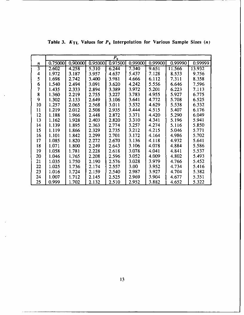
Table 3. KTL Values for Ps Interpolation for Various Sample Sizes (n)
n 0.75000 0.90000 0.95000 0.97500 0.99000 0.99900 0.99990 0.999993 2.602 4.258 5.310 6.244 7.340 9.651 11.566 13.9324 1.972 3.187 3.957 4.637 5.437 7.128 8.533 9.7565 1.698 2.742 3.400 3.981 4.666 6.112 7.311 8.3586 1.540 2.494 3.091 3.620 4.242 5.556 6.646 7.5967 1.435 2.333 2.894 3.389 3.972 5.201 6.223 7.1138 1.360 2.219 2.755 3.227 3.783 4.955 5.927 6.7759 1.302 2.133 2.649 3.106 3.641 4.772 5.708 6.52510 1.257 2.065 2.568 3.011 3.532 4.629 5.538 6.33211 1.219 2.012 2.508 2.935 3.444 4.515 5.407 6.17612 1.188 1.966 2.448 2.872 3.371 4.420 5.290 6.04913 1.162 1.928 2.403 2.820 3.310 4.341 5.196 5.94114 1.139 1.895 2.363 2.774 3.257 4.274 5.116 5.85015 1.119 1.866 2.329 2.735 3.212 4.215 5.046 5.77116 1.101 1.842 2.299 2.701 3.172 4.164 4.986 5.70217 1.085 1.820 2.272 2.670 3.136 4.118 4.932 5.64118 1.071 1.800 2.249 2.643 3.106 4.078 4.884 5.58619 1.058 1.781 2.228 2.618 3.078 4.041 4.841 5.53720 1.046 1.765 2.208 2.596 3.052 4.009 4.802 5.49321 1.035 1.750 2.190 2.576 3.028 3.979 4.766 5.45222 1.025 1.736 2.174 2.557 3.00 3.952 4.734 5.41623 1.016 1.724 2.159 2.540 2.987 3.927 4.704 5.38224 1.007 1.712 2.145 2.525 2.969 3.904 4.677 5.35125 0.999 1.702 2.132 2.510 2.952 3.882 4.652 5.322
13
SECTION 6
TEST RESULTS
The following subsections provide the total dose and dose rate results for MITRE's test ofthe TMS320C30.
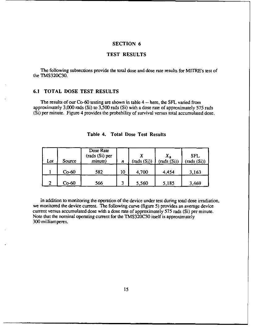
6.1 TOTAL DOSE TEST RESULTS
The results of our Co-60 testing are shown in table 4 -- here, the SFL varied fromapproximately 3,000 rads (Si) to 3,500 rads (Si) with a dose rate of approximately 575 rads(Si) per minute. Figure 4 provides the probability of survival versus total accumulated dose.
Table 4. Total Dose Test Results
Dose Rate(rads (Si) per X Xa SFL
Lot Source minute) n (rads (Si)) (rads (Si)) (rads (Si))
1 Co-60 582 10 4,700 4,454 3,163
2 Co-60 566 3 5,560 5,185 3,469
in addition to monitoring the operation of the device under test during total dose irradiation,we monitored the device current. The following curve (figure 5) provides an average devicecurrent versus accumulated dose with a dose rate of approximately 575 rads (Si) per minute.Note that the nominal operating current for the TMS320C30 itself is approximately300 milliamperes.
15

099- ............. Sample Size = 10 for EPIC-1A1 3 for EPIC-1Z
0.98 Xvme= 4,700 rad(i5,560 rad (Si)
0.97 ................................... .............. W= 3,717 rad (Si)
0.6 ..................... 4,226 rad (S)095-iit YW = 3,163 rad (Si)of urvva 0.5 .................................. .................... 3, 469 rad (Si)0.94-............................................ ....... ... ) 9 W9~0 = 2,797 rad (Si)....
2,991 2Ld&Si
0.93 1
0.92-............................... ... ...........................................................
0.91-
09-0 2500 5000 7500 10000
Total Dose [Tad (Si)I
- EPIC-lA - EPIC-1Z
Figure 4. Total Dose Probability of Survival
Average Device 0.5 - -
Current (Amps) 04
0.4-
0 1000 2000 3000 4000 5000 6000 7000
Total Accumulated Dose (rad (Si)]
Figure 5. Average Device Current versus Tetal Accumulated Dose
16

6.2 DOSE RATE TEST RESULTS
Dose rate testing consisted of both prompt characterization using a narrow pulse (20-30-nsFWHM) and delayed characterization using a wide pulse (1-ps FWHM). Both upset thresholdand dose-rate-induced latch-up phenomena were investigated. The use of the flash X-rayfacility versus the LINAC facility was based on the order in which the device lots arrived andthe availability of the particular facility at the time of their arrival.
6.2.1 Prompt Environment
Table 5 provides the results of upset threshold testing using a narrow pulse of either 20 or30 ns. Table 6 shows the results of latch-up using the narrow pulse.
Table 5. Prompt Dose Rate Upset Threshold Results (Narrow Pulse)
X Xa SFLPulse Pulse (rads (Si) (rads (Si) (rads (Si)
Lot Source Width n per second) per second) per second)
1 Flash X-ray 20 ns 10 1.2 x 10⁸ 1.1 x 10⁸ 6.8 x 10⁷
2 LINAC 30 ns 5 2.7 x 10⁸ 2.1 x 10⁸ 7.2 x 10⁷
Table 6. Prompt Dose Rate Latch-Up Results (Narrow Pulse)
Minimum MaximumLatch-Up No Latch
Pulse Pulse Devices (rads (Si) (rads (Si)Lot Source Width n Latched per second) per second)
I Flash X-ray 20 ns 10 6 1.6 x 10⁹ 3.0 x 10⁹
2 LINAC 30 ns 5 1 1.7 x 10⁹ 2.7 x 10⁹
Note the maximum levels we were able to attain using the two different pulse sources.Also note that as we observed latch-up at room temperature, we did not test for latch-up
17

conditions at elevated temperatures. Figure 6 summarizes the prompt dose rate effects byproviding the probability of no upset versus dose rate.
o0 ............. ...... Sample Size = 10for EPIC-A .0.99-.5for EPIC-1Z
0.98 Xavege = 1.2 x 10⁸ rad (Siysec
2.7 x 10 rad (Siysec0.97 ................................................ X990= 8.7 x 10⁷ rad (51)/sec.
1 .2 x 1078 rad (Siy/socProbability 0.96-............... ................ 2 107dSis
of No X99 90 = 6.8 x 10⁷ rad (SiysecUpset 0.95- 7.2 x 10 rad (Si)/sec
S99/90 = 57 x 107 rad (Si)/sec0.94 7 4:8 x 10" rad (Si)/sec
0 .9 2 . .................................... .1............ ....................................................................................................0.92-
0.91
0.9- I I 1 1 1
0 5.3 x 10 7 1.1x 10⁸ 1.6x 10 8 2.1x 10⁸ 2.6 x 10⁸ 3.2 x 10⁸
Prompt Dose Rate [rad (Si) per Second]
EPIC-1A EPIC-IZ
Figure 6. Prompt Dose Rate Probability of No Upset
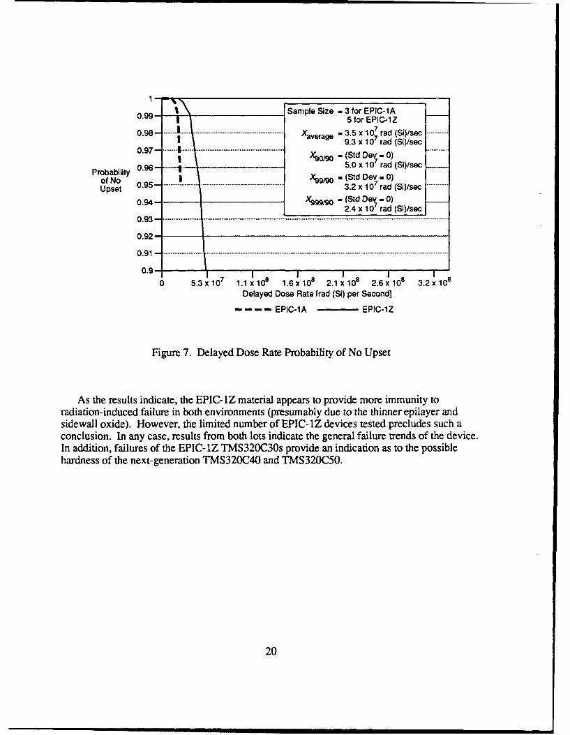
6.2.2 Delayed Environment
Tables 7 and 8 provide the result of delayed dose rate effects using a 1-gs-wide pulse forupset threshold and latch-up, respectively, with figure 7 providing the probability of no upset.As the sample standard deviation was zero for the EPIC-i A devices, we provided a pseudo-Pscurve by using the standard deviation of the EPIC-IZ material -- hence the use of the dashedline to caution the reader.
18

Table 7. Delayed Dose Rate Upset Threshold Results (Wide Pulse)
X Xa SFLPulse Pulse (rads (Si) (rads (Si) (rads (Si)
Lot Source Width n per second) per second) per second)
1 LINAC I lIs 3 3.5 x 10⁷ 3.5 x 10⁷ 3.5 x 10⁷
2 LINAC I ts 5 9.3 x 10⁷ 7.8 x 10⁷ 3.2 x 10⁷
Table 8. Delayed Dose Rate Latch-Up Results (Wide Pulse)
Minimum MaximumLatch-Up No Latch
Pulse Pulse Devices (rads (Si) (rads (Si)Lot Source Width n Latched per second) per second)
1 LINAC is 3 3 5.6 x 10⁷ 2.6 x 10⁸
2 LINAC 1 is 5 0 8.4 x 10⁸
6.3 DISCUSSION
During our testing, we observed failures of most all functional units of the TMS320C30.While it was not the goal of this testing to absolutely identify susceptible areas on the device,we did notice a predominance of interrupt-related failures as a result of both dose rate and totaldose irradiation. Our use of the serial port for communication worked well enough to detectearly failures of the device in all environments; however, that too failed during latch-up testingwhere current measurements were used to indicate such a condition. When possible, we alsoused the emulation port of the device to examine failures after testing -- this feature is availableon many new microprocessors and should be considered for future testing. Note that as thisdevice does have some dynamic logic on-chip, its inherent hardness will most likely degradewith a decrease in clock frequency. As the radiation-induced loss of charge is a direct functionof time, the slower clock frequency will provide a longer window for this phenomenon.Therefore, users of the TMS320C30 operating the device at slower clock frequencies shouldconsider this when examining our data.
19
0.99- Sample Size = 3 for EPIC-1A5 for EPIC-1Z
0.98 . ....... ...................................................... . X = 3.5 x 10⁷ rad (Si)/sec ............Xaverage 9.3 x 10 7rad (Si)Isec
0.97 . .... ................... ............................. X 0 0 = (Std Dev = 0) ...........
09 5.0 x 10⁷ rad (Si)/secProf No 0.95- . .X 99/90 = (Std Dev = 0)Upset 0.95 ................................ .......... 3.2 x 10 7 rad (S)/sec .......
0X999190 - (Std Dev - 0)2.4 x 10⁷ rad (Si)/sec0 .93 . ..................... .........................................................................................................................................
0.92-0.91 . ...................... ................. .....................................................................................................................
0.9- 1 I I 1 1
0 5.3 x 10 1.1 x 10 1.6 x 10 2.1 x 10 2.6 x 10 3.2 x 10Delayed Dose Rate frad (Si) per Second]
---- EPIC-1A EPIC-1Z
Figure 7. Delayed Dose Rate Probability of No Upset
As the results indicate, the EPIC- 1Z material appears to provide more immunity toradiation-induced failure in both environments (presumably due to the thinner epilayer andsidewall oxide). However, the limited number of EPIC-1Z devices tested precludes such aconclusion. In any case, results from both lots indicate the general failure trends of the device.In addition, failures of the EPIC-lZ TMS320C30s provide an indication as to the possiblehardness of the next-generation TMS320C40 and TMS32OC50.
20
SECTION 7
CONCLUSION
MITRE's test of the TMS320C30 resulted in failures between 4- and 5-K rads (Si) inthe total dose environment with an SFL of approximately 3-K rads (Si). In the prompt doserate environment using a 20-30-ns pulse, the device failed in the area of 1 x 10⁸ rads (Si) persecond with an SFL of approximately 7 x 10⁷ rads (Si) per second. For the delayed dose rateenvironment using a 1-gts pulse, the device failed in the area of 5 x 10⁷ rads (Si) per secondwith an SFL of approximately 3.2 x 10⁷ rads (Si) per second. We observed latch-up in bothenvironments at room temperature, at approximately 1 x 10⁹ rads (Si) per second in the promptenvironment and at approximately 1 x 10⁸ rads (Si) per second in the delayed environment.
To summarize, this test effort provides the general failure trends of the TMS320C30 butmay not reflect the full failure range due to the limited sample size (15 devices total). Testingby other organizations may provide additional data that will expand the user community'sknowledge of the full failure range of the TMS320C30.
21
LIST OF REFERENCES
1. Texas Instruments, August 1988, TMS320C3x User's Guide, Texas Instruments,Houston, Texas.
2. Wilkin, N., et al., December 1980, "Ionizing Dose Rate Effects in Microprocessors,"IEEE Transactions on Nuclear Science, pp. 1420-1424.
3. Koga, R., et al., December 1985, "Techniques of Microprocessor Testing and SEU-RatePrediction," IEEE Transactions on Nuclear Science, pp. 4219-4224.
4. Elder, J. H., et al., December 1988, "A Method for Characterizing a Microprocessor'sVulnerability to SEU," IEEE Transactions on Nuclear Science, pp. 1678-1681.
5. Marks, K., and P. Measel, December 1982, "Total Dose Test Results for the 8086Microprocessor," IEEE Transactions on Nuclear Science, pp. 1662-1664.
6. Harboe-Sorensen, R., et al., December 1986, "The SEU Risk Assessment of the Z80A,8086 and 80C86 Microprocessors Intended for Use in a Low Altitude Polar Orbit," IEEETransactions on Nuclear Science, pp. 1626-1631.
*7. Bumbaugh, M., and L. Hitt, (No Date), Ionizing Radiation Test Results on the Intel80186 and 80286 Microprocessors, HDL Technical Report (No Number).
*8. (No Author, No Date), Radiation Characterization Data for the Intel 80386 32-BitMicroprocessor.
9. Thomlinson, J., et al., December 1987, "The SEU and Total Dose Response of theInmos Transputer," IEEE Transactions on Nuclear Science, pp. 1803-1808.
10. Guenzer, C. S., et al., December 1981, "Single Event Upsets in NMOSMicroprocessors," IEEE Transactions on Nuclear Science, pp. 4010-4015.
*11. Bumbaugh, M. E., June 1989, Ionizing Radiation Test Results on the Motorola 68020Microprocessor, HDL TM-89-4.
12. Will, W. E., et al., December 1981, "Total Dose Response of the Z80A and Z8002Microprocessors," IEEE Transactions on Nuclear Science, pp. 4046-4050.
13. Johnston, A. H., December 1983, "Annealing of Total Dose Damage in the Z80AMicroprocessor," IEEE Transactions on Nuclear Science, pp. 4251-4255.
14. Cusick, J., et al., December 1985, "SEU Vulnerability of the Zilog Z-80 and NSC-800Microprocessors," IEEE Transactions on Nuclear Science, pp. 4206-4211.
23

I5. Eisen, H. (of Harry Diamond Laboratories), 2 July 1990, private communication.
* 16. Bumbaugh, M. (of Harry Diamond Laboratories), 2 July 1990, private communication.
* 17. Myers, D. (of Myers Associates), 2 July 1990, private communication.
*18. "Steady State Total Dose Irradiation Procedure," 29 May 1987, MIL-STD-883C throughNotice 5, Method 1019.3.
*19. "Dose Rate Threshold for Upset of Digital Microcircuits," 15 August 1984,
MIL-STD-883C through Notice 5, Method 1021.1.
*20. "Radiation-Induced Latch-up Test Procedure," 16 May 1979, MIL-STD-883C throughNotice 5, Method 1020.
21. Messenger, G. C., and E.L. Steele, December 1968, "Statistical Modeling ofSemiconductor Devices for the TREE Environment," IEEE Transactions on NuclearScience, pp. 133-139.
*22. "Ionizing Radiation and Neutron Displacement Damage Hardness Assurance Guidelinesfor Semiconductor Devices and Microcircuits," November 1990, Sixth Draft ofMIL-HDBK-279/280.
*These documents have not been reviewed by the Directorate for Security Review and aretherefore not available for public dissemination.
24
GLOSSARY
ACRONYMS
ALU arithmetic logic unitARA U auxiliary register arithmetic unit
CMOS complimentary metal-oxide semiconductorCo-60 Cobalt-60
DMA direct memory accessDOD Department of DefenseDSP digital signal processor/processing
FWHM full-width half maximum
NIST National Institute of Standards and Technology
PGA pin grid array
RADC Rome Air Development Center
SFL statistical failure level
TI Texas InstrumentsTLD thermoluminescent dosimeterTTL transistor-transistor-logic
SYMBOLS
KTL one-sided tolerance factor
Ps probability of survival
s standard deviation
X sample meanX2 adjusted mean
25

![HUMIDITY & TEMPERATURE SENSOR - D'Addario ... 3 Humidity & Temperature Sensor [HTS] Sensor de Humedad y Temperatura Dètecteur D'humiditè et de Tempèrature Luftfeuchtigkeits-und](https://img.pdfslide.us/doc/110x75/5ac330227f8b9a2b5c8ba250/humidity-temperature-sensor-daddario-3-humidity-temperature-sensor-hts.jpg)