Embed Size (px)
Citation preview
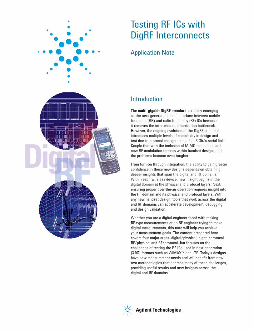
Testing RF ICs with DigRF Interconnects
Application Note
Introduction
The multi-gigabit DigRF standard is rapidly emerging
as the next-generation serial interface between mobile
baseband (BB) and radio frequency (RF) ICs because
it removes the inter-chip communication bottleneck.
However, the ongoing evolution of the DigRF standard
introduces multiple levels of complexity in design and
test due to protocol changes and a fast 3 Gb/s serial link.
Couple that with the inclusion of MIMO techniques and
new RF modulation formats within handset designs and
the problems become even tougher.
From turn-on through integration, the ability to gain greater
confidence in these new designs depends on obtaining
deeper insights that span the digital and RF domains.
Within each wireless device, new insight begins in the
digital domain at the physical and protocol layers. Next,
ensuring proper over-the-air operation requires insight into
the RF domain and its physical and protocol layers. With
any new handset design, tools that work across the digital
and RF domains can accelerate development, debugging
and design validation.
Whether you are a digital engineer faced with making
RF-type measurements or an RF engineer trying to make
digital measurements, this note will help you achieve
your measurement goals. The content presented here
covers four major areas–digital/physical, digital/protocol,
RF/physical and RF/protocol–but focuses on the
challenges of testing the RF ICs used in next-generation
(3.9G) formats such as WiMAX™ and LTE. Today’s designs
have new measurement needs and will benefit from new
test methodologies that address many of these challenges,
providing useful results and new insights across the
digital and RF domains.
DigitalRFRFRFRFRFRF
2
The move to 3.9G formats such as LTE and WiMAX is
driving fundamental changes in the under-lying architecture
of mobile handsets. For R&D teams developing, integrating
and validating 3.9G devices, challenges abound in the
embedded technologies and the required measurements.
These challenges exist in the physical and protocol layers
of the digital and RF domains–and they span the domains:
• The former analog BB-to-RF IC communication link is
now a high-speed serial digital interface.
• Testing requires different equipment and a different
methodology because analog sources can no longer
be used to stimulate the RF IC on the BB interface.
• The combination of the DigRF protocol with the
wireless protocol creates a”dual protocol stack”
that complicates characterization and validation.
• The information flowing through the interface between
the BB and RF ICs includes data and control traffic.
• Information transfers must comply with very strict time
constraints (time determinism).
In 3.9G devices, the presence of the BB-to-RF IC digital
interface has a strong effect on design and test processes.
For example, high-speed digital signals may suffer from
impaired signal integrity and a degraded bit-error rate
(BER), and these measurements require special measure-
ment tools and techniques. Successful characterization
and validation of the dual protocol stack requires a test
infrastructure that provides insights into all layers. Dealing
with data and control traffic depends on test equipment
that can configure, analyze and create mixed traffic.
Testing the serial digital IQ interface to the RF IC requires
DigRF-compatible stimulus and analysis tools. The
test environment must also precisely measure the timing
of each frame and detect time-constraint violations.
A closer look at each of these challenges and the
associated considerations for testing will provide
additional context for our discussion.
Digital serial link
The BB-to-RF IC connections have undergone an archi-
tectural shift from analog or proprietary parallel buses to
serializer/deserializer (SERDES) links for several reasons.
First, serial links eliminate parallel-bus clock skew, reduce
the number of pins and traces, and enable power savings
with bus sleep modes. However, at gigabit-per-second
data rates–and with channel flight times longer than a bit
Testing RF-ICs: New challenges
period–signal integrity becomes a major concern. Under
these conditions, high-speed analog effects can impair
signal quality and degrade link BER.
As with other serial buses, the new DigRF standards employ
data encoding mechanisms (8b/10b) along with embedded
clocks and protocol state machines for link and transaction
operations to guarantee reliable data transfer. To analyze the
data, the embedded clock must be extracted before the data
can be decoded and fully analyzed. A clear understanding
of clock recovery, encode/decode protocols and real-time
measurements is critical for success. Most general-purpose
measurement tools cannot understand DigRF-specific
signals and information encoding so can therefore provide
only raw information about the digital data.
RF IC test methodology
Digital IQ data and control information is now packetized
and transferred between the BB and RF ICs over the DigRF
interface. Previously, RF engineers and validation teams
used analog sources to stimulate the RF IC on the analog
IQ interface. This is no longer the standard interface, so
new tools are needed to enable the same RF physical
measurements through the DigRF digital serial interface.
This is complicated by the fact that some components may
not be ready or available for tests during the early stages of
development. For example, it may be necessary to test the
RF IC before the BB IC is available. This can be remedied
with a test environment that has the capability to simulate
a missing device and includes DigRF stimulus and analysis
tools that operate in concert with traditional RF tools.
Dual protocol stack
Similar to many other serial buses, the DigRF interface is
described as a stack of multiple protocol layers in which
each layer has a specific function and mode of operation.
These layers grow in abstraction from the physical layer
to the application or software layer, and include the link
layer (or mode of operation of the bus), the data-encoding
scheme, the frame structure, the flow control, the error
handling mechanism, and so on. In this note, we will refer
to this as the digital protocol stack.
Ensuring that an RF IC properly interoperates with a BB IC
requires verification that all layers of the digital protocol
stack are designed (and operate) in accordance with the
DigRF specification. If any layer fails, data will not be
3
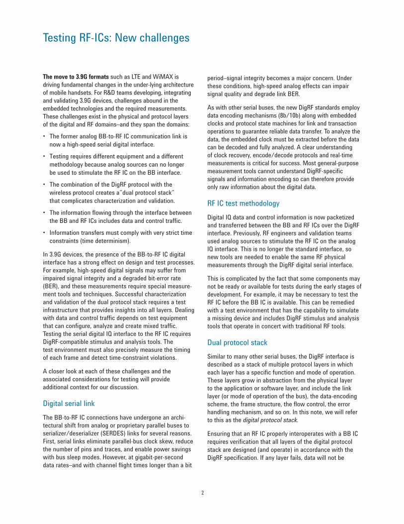
Figure 1. This example of a digital protocol viewer shows data
from a DigRF V3 bus.
Figure 2. The Agilent DigRF test dual interface presents
information from the digital protocol layers (bit-and packet-level
view, see Figure 1) and the RF physical information (modulation
analysis) from the same measurement.
reliably transferred between the RF and BB ICs. A suitable
test environment must provide analysis and stimulus
capabilities on the entire digital protocol stack (Figure 1).
DigRF is designed to be used in mobile devices, and it is
unlike most serial buses because there is another protocol
stack “encapsulated” within the digital interface–and this
stack represents the mobile handset’s wireless-protocol
operation (e.g., GSM, WCDMA, LTE, WiMAX). As with
other protocols, this stack spans from the RF physical layer
to the RF application layer. Throughout this note, we will
refer to this as the wireless protocol stack.
Things can become confusing as the physical and protocol
layers of the two stacks are intermixed. Because the RF
physical-layer information is encapsulated in the payload
of DigRF frames, it is seen as existing “above” the DigRF
protocol layer. This is different from typical layering
schemes in which the physical layer resides on the bottom
of the stack and the protocol layers are on the top.
The characterization and validation of a DigRF-enabled RF
IC will require measurement of each layer of the digital and
RF protocol stacks. This requires a test infrastructure that
provides insight on all layers (Figure 2). From a stimulus
point of view, the ability to test an RF IC under real-world
conditions requires a test environment that can encap-
sulate IQ stimulus data within DigRF traffic to create the
required dual-stack stimulus model.
Mixed traffi c
The information flowing between RF and BB ICs consists
of IQ data encapsulated in DigRF frames as well as control
information being sent from the BB IC to the RF IC. This
control information stays within the RF IC. Here are some
examples of control traffic:
• Ping: The BB IC uses the “Are you there?” command
to check if the RF IC is enabled to respond.
• Loopback: Turning this on configures the RF IC
in loopback mode.
• Power: Changing transmit output power level is a
common action.
When testing an RF IC, proper validation requires test
equipment that can configure and create this mix of control
and data traffic (Figure 3). To test an RF IC, the stimulus
environment must be able to insert RF-IC control informa-
tion within the IQ data flow.
Time determinism
Information transfers between the RF and BB ICs must
comply with very strict time constraints: The right data
arriving at the wrong time is incorrect data. Therefore, it
is important for the test environment to precisely measure
when each frame was sent from one IC to the other and
provide real-time detection of time-constraint violations.
Figure 3. An example of control commands mixed with data traffi c.
Because these commands may not be in the original stimulus fi le,
it may be necessary to send them on-the-fl y to the RF IC.
4
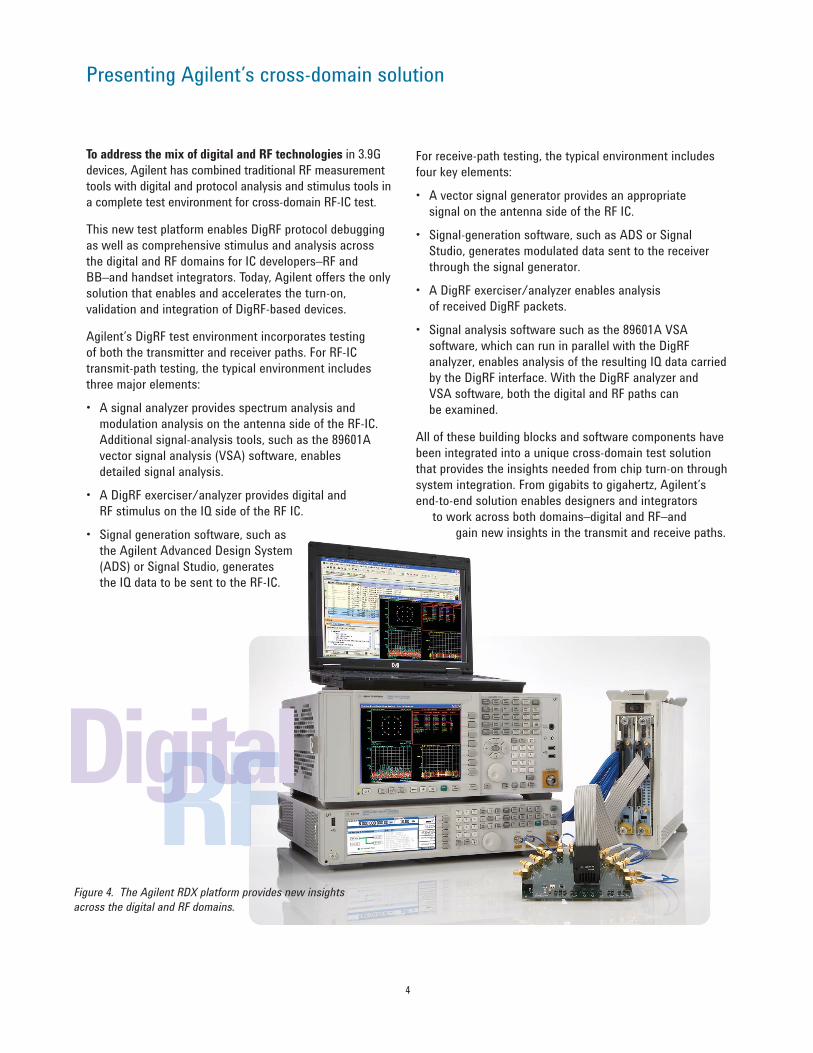
To address the mix of digital and RF technologies in 3.9G
devices, Agilent has combined traditional RF measurement
tools with digital and protocol analysis and stimulus tools in
a complete test environment for cross-domain RF-IC test.
This new test platform enables DigRF protocol debugging
as well as comprehensive stimulus and analysis across
the digital and RF domains for IC developers–RF and
BB–and handset integrators. Today, Agilent offers the only
solution that enables and accelerates the turn-on,
validation and integration of DigRF-based devices.
Agilent’s DigRF test environment incorporates testing
of both the transmitter and receiver paths. For RF-IC
transmit-path testing, the typical environment includes
three major elements:
• A signal analyzer provides spectrum analysis and
modulation analysis on the antenna side of the RF-IC.
Additional signal-analysis tools, such as the 89601A
vector signal analysis (VSA) software, enables
detailed signal analysis.
• A DigRF exerciser/analyzer provides digital and
RF stimulus on the IQ side of the RF IC.
• Signal generation software, such as
the Agilent Advanced Design System
(ADS) or Signal Studio, generates
the IQ data to be sent to the RF-IC.
Presenting Agilent’s cross-domain solution
For receive-path testing, the typical environment includes
four key elements:
• A vector signal generator provides an appropriate
signal on the antenna side of the RF IC.
• Signal-generation software, such as ADS or Signal
Studio, generates modulated data sent to the receiver
through the signal generator.
• A DigRF exerciser/analyzer enables analysis
of received DigRF packets.
• Signal analysis software such as the 89601A VSA
software, which can run in parallel with the DigRF
analyzer, enables analysis of the resulting IQ data carried
by the DigRF interface. With the DigRF analyzer and
VSA software, both the digital and RF paths can
be examined.
All of these building blocks and software components have
been integrated into a unique cross-domain test solution
that provides the insights needed from chip turn-on through
system integration. From gigabits to gigahertz, Agilent’s
end-to-end solution enables designers and integrators
to work across both domains–digital and RF–and
gain new insights in the transmit and receive paths.
DigitalRFgitagitaFigure 4. The Agilent RDX platform provides new insights
across the digital and RF domains.
5
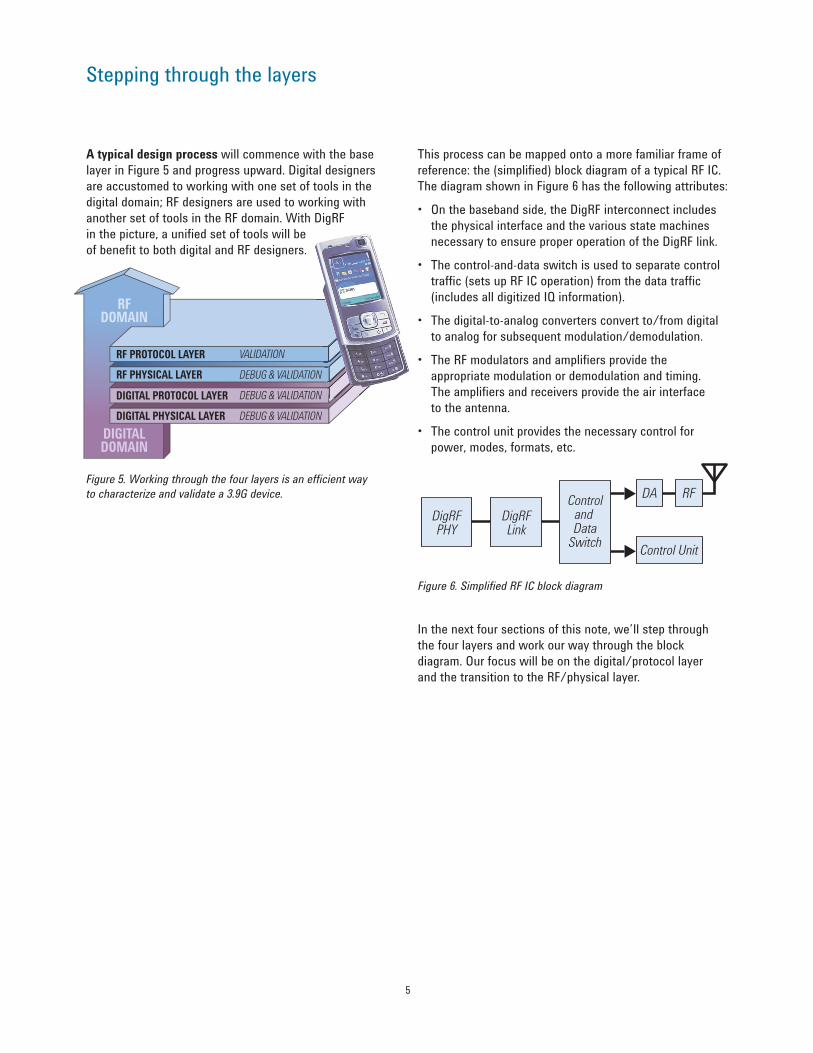
Figure 5. Working through the four layers is an effi cient way
to characterize and validate a 3.9G device.
Stepping through the layers
A typical design process will commence with the base
layer in Figure 5 and progress upward. Digital designers
are accustomed to working with one set of tools in the
digital domain; RF designers are used to working with
another set of tools in the RF domain. With DigRF
in the picture, a unified set of tools will be
of benefit to both digital and RF designers.
This process can be mapped onto a more familiar frame of
reference: the (simplified) block diagram of a typical RF IC.
The diagram shown in Figure 6 has the following attributes:
• On the baseband side, the DigRF interconnect includes
the physical interface and the various state machines
necessary to ensure proper operation of the DigRF link.
• The control-and-data switch is used to separate control
traffic (sets up RF IC operation) from the data traffic
(includes all digitized IQ information).
• The digital-to-analog converters convert to/from digital
to analog for subsequent modulation/demodulation.
• The RF modulators and amplifiers provide the
appropriate modulation or demodulation and timing.
The amplifiers and receivers provide the air interface
to the antenna.
• The control unit provides the necessary control for
power, modes, formats, etc.
In the next four sections of this note, we’ll step through
the four layers and work our way through the block
diagram. Our focus will be on the digital/protocol layer
and the transition to the RF/physical layer.
DIGITAL PHYSICAL LAYER DEBUG & VALIDATION
DIGITAL PROTOCOL LAYER DEBUG & VALIDATION
RF PHYSICAL LAYER
RF PROTOCOL LAYER
DEBUG & VALIDATION
VALIDATION
RFDOMAIN
DIGITALDOMAIN
DigRFPHY
DigRFLink
Control Unit
DA RFControl
and Data
Switch
Figure 6. Simplifi ed RF IC block diagram
6
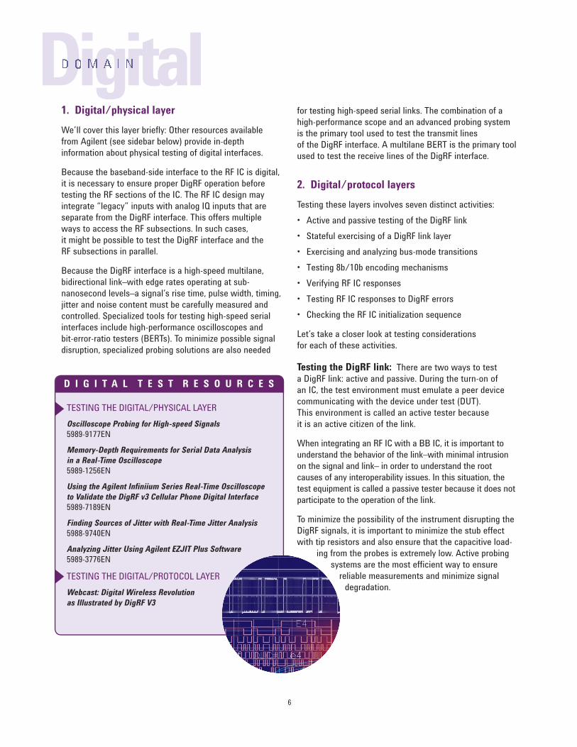
D I G I T A L T E S T R E S O U R C E S
1. Digital/physical layer
We’ll cover this layer briefly: Other resources available
from Agilent (see sidebar below) provide in-depth
information about physical testing of digital interfaces.
Because the baseband-side interface to the RF IC is digital,
it is necessary to ensure proper DigRF operation before
testing the RF sections of the IC. The RF IC design may
integrate “legacy” inputs with analog IQ inputs that are
separate from the DigRF interface. This offers multiple
ways to access the RF subsections. In such cases,
it might be possible to test the DigRF interface and the
RF subsections in parallel.
Because the DigRF interface is a high-speed multilane,
bidirectional link–with edge rates operating at sub-
nanosecond levels–a signal’s rise time, pulse width, timing,
jitter and noise content must be carefully measured and
controlled. Specialized tools for testing high-speed serial
interfaces include high-performance oscilloscopes and
bit-error-ratio testers (BERTs). To minimize possible signal
disruption, specialized probing solutions are also needed
for testing high-speed serial links. The combination of a
high-performance scope and an advanced probing system
is the primary tool used to test the transmit lines
of the DigRF interface. A multilane BERT is the primary tool
used to test the receive lines of the DigRF interface.
2. Digital/protocol layers
Testing these layers involves seven distinct activities:
• Active and passive testing of the DigRF link
• Stateful exercising of a DigRF link layer
• Exercising and analyzing bus-mode transitions
• Testing 8b/10b encoding mechanisms
• Verifying RF IC responses
• Testing RF IC responses to DigRF errors
• Checking the RF IC initialization sequence
Let’s take a closer look at testing considerations
for each of these activities.
Testing the DigRF link: There are two ways to test
a DigRF link: active and passive. During the turn-on of
an IC, the test environment must emulate a peer device
communicating with the device under test (DUT).
This environment is called an active tester because
it is an active citizen of the link.
When integrating an RF IC with a BB IC, it is important to
understand the behavior of the link–with minimal intrusion
on the signal and link– in order to understand the root
causes of any interoperability issues. In this situation, the
test equipment is called a passive tester because it does not
participate to the operation of the link.
To minimize the possibility of the instrument disrupting the
DigRF signals, it is important to minimize the stub effect
with tip resistors and also ensure that the capacitive load-
ing from the probes is extremely low. Active probing
systems are the most efficient way to ensure
reliable measurements and minimize signal
degradation.
TESTING THE DIGITAL/PHYSICAL LAYER
Oscilloscope Probing for High-speed Signals
5989-9177EN
Memory-Depth Requirements for Serial Data Analysis
in a Real-Time Oscilloscope
5989-1256EN
Using the Agilent Infiniium Series Real-Time Oscilloscope
to Validate the DigRF v3 Cellular Phone Digital Interface
5989-7189EN
Finding Sources of Jitter with Real-Time Jitter Analysis
5988-9740EN
Analyzing Jitter Using Agilent EZJIT Plus Software
5989-3776EN
TESTING THE DIGITAL/PROTOCOL LAYER
Webcast: Digital Wireless Revolution
as Illustrated by DigRF V3
DigitalDigiDigi
7
A stateful test environment makes it possible to test
the following bus modes:
• Transitions from sleep mode to active mode
• Retry sequences
• Flow-control mechanisms that require the sender
to slow down or speed up the traffic
• Emulation of a bus and its dynamic physical
characteristics that may change in response to
protocol events (e.g., termination, voltage level )
Most stateful test platforms (or exercisers) are bidirectional
because they must constantly listen to the DUT in order
to interact with it. The Agilent RDX test platform is
a DigRF exerciser, enabling stateful stimulus of the RF IC.
Exercising and analyzing bus-mode transitions: Reduced power consumption will provide longer battery
life in mobile devices. To support this need–and optimize
both power consumption and performance– the DigRF bus
has been designed to operate in multiple high-speed and
low-power modes. When no data is being sent, the bus
shifts into a sleep mode that requires very little power.
When data must be transferred, the bus can quickly wake
up and start transferring data.
One key feature of a suitable DigRF test environment is the
ability to properly support power-management features and
the associated bus transitions. From a stimulus point of
view, the test platform must deterministically support these
modes so that it can check DUT mode transitions and
verify specification-compliant execution.
From an analysis point of view, it is necessary to perform
two types of measurements with one analysis module;
track the transitions and capture the data between the
transitions, especially when the bus wakes up. In this
application, instrumentation lock time is critical because
it needs to capture data from the embedded clock. If the
test instrument’s lock time is slower than that of the DUT,
it cannot reliably measure the behavior of the device and
may lose the initial data elements after the bus wakes
up. The Agilent RDX test platform includes a multipath
clock-recovery mechanism to capture data during
very fast bus-mode transitions.
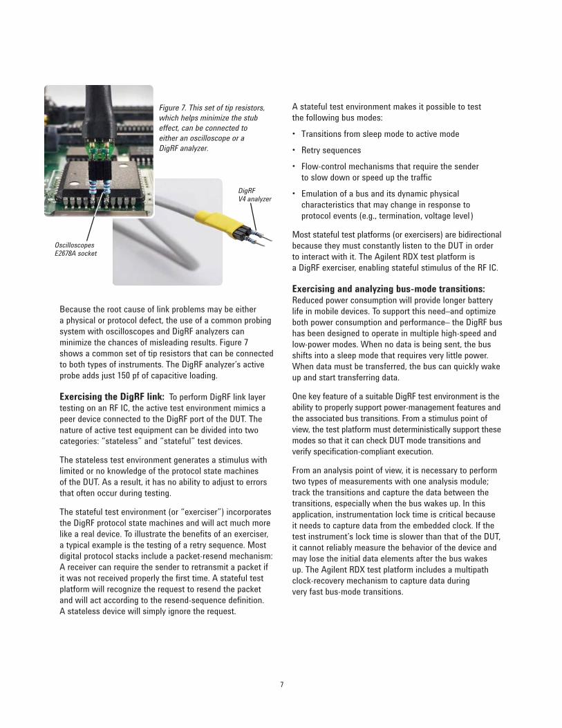
Because the root cause of link problems may be either
a physical or protocol defect, the use of a common probing
system with oscilloscopes and DigRF analyzers can
minimize the chances of misleading results. Figure 7
shows a common set of tip resistors that can be connected
to both types of instruments. The DigRF analyzer’s active
probe adds just 150 pf of capacitive loading.
Exercising the DigRF link: To perform DigRF link layer
testing on an RF IC, the active test environment mimics a
peer device connected to the DigRF port of the DUT. The
nature of active test equipment can be divided into two
categories: “stateless” and “stateful” test devices.
The stateless test environment generates a stimulus with
limited or no knowledge of the protocol state machines
of the DUT. As a result, it has no ability to adjust to errors
that often occur during testing.
The stateful test environment (or “exerciser”) incorporates
the DigRF protocol state machines and will act much more
like a real device. To illustrate the benefits of an exerciser,
a typical example is the testing of a retry sequence. Most
digital protocol stacks include a packet-resend mechanism:
A receiver can require the sender to retransmit a packet if
it was not received properly the first time. A stateful test
platform will recognize the request to resend the packet
and will act according to the resend-sequence definition.
A stateless device will simply ignore the request.
Figure 7. This set of tip resistors,
which helps minimize the stub
effect, can be connected to
either an oscilloscope or a
DigRF analyzer.
OscilloscopesE2678A socket
DigRFV4 analyzer
8
DigitalTesting encoding mechanisms: The 8b/10b transmission
code converts a byte-wide datastream of random ones
and zeros into a DC-balanced stream of ones and zeros.
The code also provides sufficient signal transitions to
enable reliable clock recovery. The average number of
ones and zeros in the serial stream must be maintained
at equal or nearly-equal levels.
When testing a DigRF link, it is important to ensure that
the DUT properly encodes and decodes the data. It is also
essential to properly identify disparity errors and analyze
how the DUT detects and recovers from such exceptions.
Disparity errors tend to occur infrequently and the analyzer
triggering mechanisms must include real-time detection
of such errors.
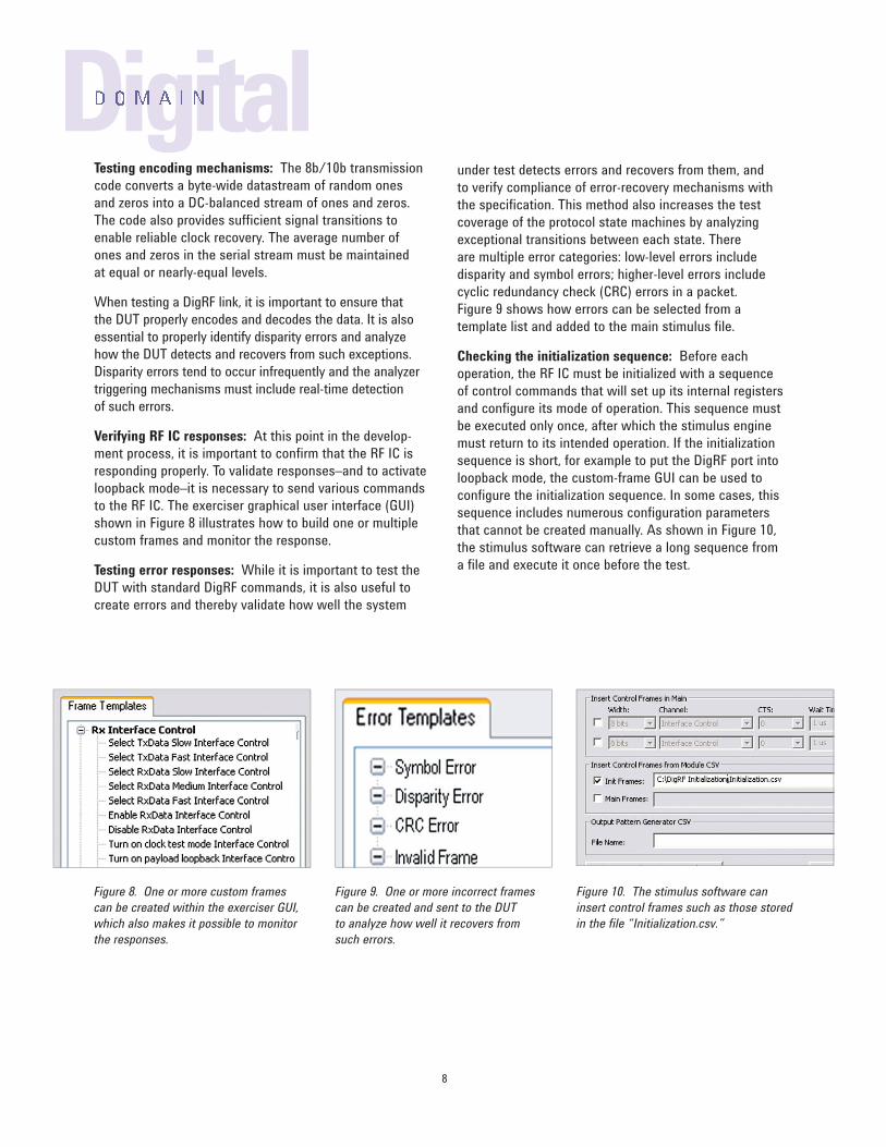
Verifying RF IC responses: At this point in the develop-
ment process, it is important to confirm that the RF IC is
responding properly. To validate responses–and to activate
loopback mode–it is necessary to send various commands
to the RF IC. The exerciser graphical user interface (GUI)
shown in Figure 8 illustrates how to build one or multiple
custom frames and monitor the response.
Testing error responses: While it is important to test the
DUT with standard DigRF commands, it is also useful to
create errors and thereby validate how well the system
under test detects errors and recovers from them, and
to verify compliance of error-recovery mechanisms with
the specification. This method also increases the test
coverage of the protocol state machines by analyzing
exceptional transitions between each state. There
are multiple error categories: low-level errors include
disparity and symbol errors; higher-level errors include
cyclic redundancy check (CRC) errors in a packet.
Figure 9 shows how errors can be selected from a
template list and added to the main stimulus file.
Checking the initialization sequence: Before each
operation, the RF IC must be initialized with a sequence
of control commands that will set up its internal registers
and configure its mode of operation. This sequence must
be executed only once, after which the stimulus engine
must return to its intended operation. If the initialization
sequence is short, for example to put the DigRF port into
loopback mode, the custom-frame GUI can be used to
configure the initialization sequence. In some cases, this
sequence includes numerous configuration parameters
that cannot be created manually. As shown in Figure 10,
the stimulus software can retrieve a long sequence from
a file and execute it once before the test.
Figure 8. One or more custom frames
can be created within the exerciser GUI,
which also makes it possible to monitor
the responses.
Figure 9. One or more incorrect frames
can be created and sent to the DUT
to analyze how well it recovers from
such errors.
Figure 10. The stimulus software can
insert control frames such as those stored
in the fi le “Initialization.csv.”
DigiDigi
9
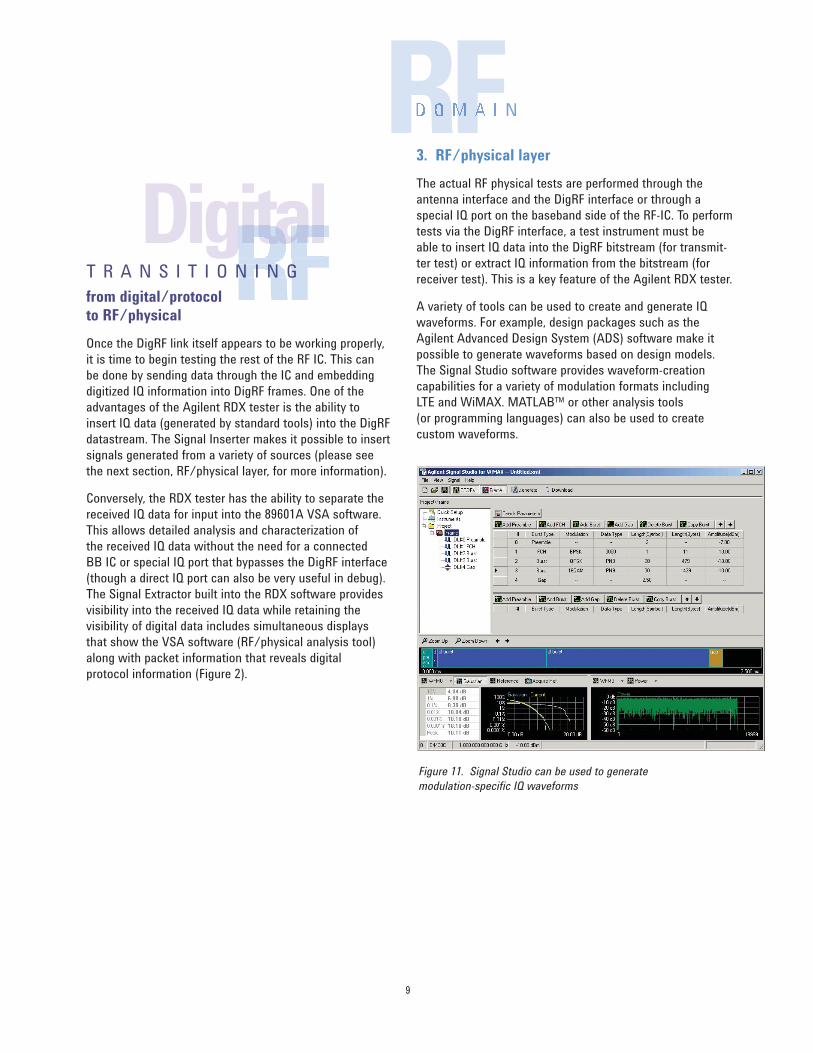
Figure 11. Signal Studio can be used to generate
modulation-specifi c IQ waveforms
from digital/protocol to RF/physical
Once the DigRF link itself appears to be working properly,
it is time to begin testing the rest of the RF IC. This can
be done by sending data through the IC and embedding
digitized IQ information into DigRF frames. One of the
advantages of the Agilent RDX tester is the ability to
insert IQ data (generated by standard tools) into the DigRF
datastream. The Signal Inserter makes it possible to insert
signals generated from a variety of sources (please see
the next section, RF/physical layer, for more information).
Conversely, the RDX tester has the ability to separate the
received IQ data for input into the 89601A VSA software.
This allows detailed analysis and characterization of
the received IQ data without the need for a connected
BB IC or special IQ port that bypasses the DigRF interface
(though a direct IQ port can also be very useful in debug).
The Signal Extractor built into the RDX software provides
visibility into the received IQ data while retaining the
visibility of digital data includes simultaneous displays
that show the VSA software (RF/physical analysis tool)
along with packet information that reveals digital
protocol information (Figure 2).
3. RF/physical layer
The actual RF physical tests are performed through the
antenna interface and the DigRF interface or through a
special IQ port on the baseband side of the RF-IC. To perform
tests via the DigRF interface, a test instrument must be
able to insert IQ data into the DigRF bitstream (for transmit-
ter test) or extract IQ information from the bitstream (for
receiver test). This is a key feature of the Agilent RDX tester.
A variety of tools can be used to create and generate IQ
waveforms. For example, design packages such as the
Agilent Advanced Design System (ADS) software make it
possible to generate waveforms based on design models.
The Signal Studio software provides waveform-creation
capabilities for a variety of modulation formats including
LTE and WiMAX. MATLAB™ or other analysis tools
(or programming languages) can also be used to create
custom waveforms.
T R A N S I T I O N
RFNRFRFDigital
RFN I N GN I N G
italgital
10
As a specific example, Agilent N7624B Signal Studio for
3GPP LTE enables creation of standards-based 3GPP LTE
signals that are compliant with 3GPP Release 8 (March
2008 version). With this software, you can configure the
standards-based test signals needed to verify RF uplink
and downlink performance (by measuring EVM, ACLR and
CCDF) and also create fully coded (transport and physical
layer) standards-based test signals for early receiver testing
using block error rate (BLER) measurements.
The RDX DigRF tester includes a signal-inserter tool
that translates IQ data into a format that is suitable for
stimulus. It also allows insertion of control frames,
time-accurate strobe messages and status messages.
The end result will be a stimulus file that contains
four items:
• The RF IC initialization sequence (control traffic)
• Data frames containing digitized IQ information
• On-the-fly control frames
• Time-accurate strobe (TAS) messages
Debugging and qualification of an RF IC’s RF subsystem
involves extensive testing and verification of three paths:
transmitter, receiver and control. Amplifier linearity,
control algorithms, modulation quality, and a host of other
items, must also be checked.
The actual sequence of RF/physical tests to be performed
depends on whichever modulation formats the RF IC is
designed to handle. Please see the sidebar below for
Agilent resources that cover suggested RF/physical-layer
tests for various modulation formats.
4. RF/protocol layer
Testing this layer generally begins later in the process
of designing and integrating the chipset and the overall
system. As a result, it has relatively little bearing on
the DigRF subsystem so is not covered here. Other
resources available from Agilent provide greater detail
(see sidebar below).
RFNRFRF
R F T E S T R E S O U R C E S
TESTING THE RF/PHYSICAL LAYER
3GPP Long Term Evolution: System Overview,
Product Development and Test Challenges
5989-8139EN (Available at: www.agilent.com/find/LTE )
Mobile WiMAX ™ PHY Layer (RF) Operation
and Measurement
5989-8309EN
IEEE 802.16e WiMAX OFDMA Signal Measurements
and Troubleshooting
5989-2382EN
WiMAX Concepts and RF Measurements
5988-2027EN
Additional WiMAX resources are available online at
www.agilent.com/find/wimax
TESTING THE RF/PHYSICAL LAYER
Webcast: Testing Mobile WiMAXRadios from
Pre-Certification Through Manufacturing
seminar2.techonline.com/s/agilent_sep2806
11
Conclusion Related Literature
The multi-gigabit DigRF standard is rapidly emerging
as the next-generation serial interface between mobile
BB and RF ICs because it removes the inter-chip
communication bottleneck. However, it also creates
measurement challenges that exist in–and span–
the physical and protocol layers of the digital and RF
domains. These challenges are compounded by the
capabilities of previous-generation test tools. To truly
understand what’s happening in DigRF-based systems,
a unified set of tools will be of benefit to both digital
and RF designers.
To address these issues, Agilent has combined traditional
RF measurement tools with digital and protocol analysis
and stimulus tools in a complete test environment for
cross-domain RF-IC test. The new Agilent RDX test
platform enables DigRF protocol debugging as well as
comprehensive stimulus and analysis across the digital
and RF domains for IC developers–BB and RF–and
handset integrators. The RDX platform is particularly
useful when testing the RF ICs used in next-generation
wireless devices: it addresses new measurement
needs and enables new test methodologies that span
the digital and RF domains.
Today, Agilent’s solution is the only one that enables
and accelerates the turn-on, validation and integration
of DigRF -based devices. From gigabits to gigahertz, our
end-to-end solution enables designers and integrators
to work across both domains–digital or RF–and apply
the new test methodologies needed to gain deeper
insights into the transmit and receive paths of the
RF ICs used in 3.9G devices.
• Agilent DigRF solutions brochure,
5989-9400EN
• Agilent RDX Test Solutions for DigRF V4 data sheet,
5989-9575EN
Remove all doubt
Our repair and calibration services
will get your equipment back to you,
performing like new, when prom-
ised. You will get full value out of
your Agilent equipment through-
out its lifetime. Your equipment
will be serviced by Agilent-trained
technicians using the latest factory
calibration procedures, automated
repair diagnostics and genuine parts.
You will always have the utmost
confi dence in your measurements.
For information regarding self
maintenance of this product, please
contact your Agilent offi ce.
Agilent offers a wide range of ad-
ditional expert test and measure-
ment services for your equipment,
including initial start-up assistance,
onsite education and training, as
well as design, system integration,
and project management.
For more information on repair and
calibration services, go to:
www.agilent.com/find/removealldoubt
www.agilent.com/find/emailupdates
Get the latest information on the
products and applications you select.
www.lxistandard.org
LXI is the LAN-based successor to
GPIB, providing faster, more effi cient
connectivity. Agilent is a founding
member of the LXI consortium.
www.agilent.com
www.agilent.com/find/DigRF
For more information on Agilent Technologies’ products, applications or services, please contact your local Agilent office.
The complete list is available at:
www.agilent.com/find/contactus
AmericasCanada (877) 894-4414 Latin America 305 269 7500United States (800) 829-4444
Asia PacificAustralia 1 800 629 485China 800 810 0189Hong Kong 800 938 693India 1 800 112 929Japan 0120 (421) 345Korea 080 769 0800Malaysia 1 800 888 848Singapore 1 800 375 8100Taiwan 0800 047 866Thailand 1 800 226 008
Europe & Middle EastAustria 01 36027 71571Belgium 32 (0) 2 404 93 40 Denmark 45 70 13 15 15Finland 358 (0) 10 855 2100France 0825 010 700* *0.125 €/minute
Germany 07031 464 6333 Ireland 1890 924 204Israel 972-3-9288-504/544Italy 39 02 92 60 8484Netherlands 31 (0) 20 547 2111Spain 34 (91) 631 3300Sweden 0200-88 22 55Switzerland 0800 80 53 53United Kingdom 44 (0) 118 9276201Other European Countries: www.agilent.com/find/contactusRevised: July 2, 2009
Product specifi cations and descriptions in this document subject to change without notice.
© Agilent Technologies, Inc. 2008, 2009Printed in USA, September 11, 20095989-9885EN
“WiMAX,” “Mobile WiMAX,” “WiMAX Forum,” the WiMAX
Forum logo, “WiMAX Forum Certifi ed” and the WiMAX Forum
Certifi ed logo are trademarks of the WiMAX Forum
MATLAB is a U.S. registered trademark of The MathWorks, Inc.
Gain greater confi dence in your DigRF designs
We’ve united our industry-leading
instrumentation and software in an
integrated platform for cross-domain
digital/RF testing at the physical
and protocol layers. From turn-on
through integration, from gigabits to
gigahertz, Agilent offers an end-to-
end solution that enables you to work
within your preferred domain–digital
or RF–and gain new insights. Every
step of the way, Agilent offers
solutions that can help you quickly
characterize and integrate your devices
and get them to market faster.