Embed Size (px)
Citation preview
Testing of a First-Generation
Dynamically Programmable Gate Array
by
Edward F. Tau
Bachelors of Science in Electrical Engineering and Computer Science
Submitted to the Department of Electrical Engineering and Computer Sciencein partial fulfillment of the requirements for the degree of
Masters of Engineering in Electrical Engineering and Computer Science
at the
MASSACHUSETTS INSTITUTE OF TECHNOLOGY
June 1996
@ Edward F. Tau, MCMXCVI. All rights reserved.
The author hereby grants to MIT permission to reproduce and distribute publiclypaper and electronic copies of this thesis document in whole or in part, and to grant
others the right to do so.
A uthor ......... ...... . . .................Department of Electrical Engineering and Computer Science
May 28, 1996
-7771
Certified byDr. oma ellige night, Jr.
Senior Research Scientist, MIT Artificial Intelligence LaboratoryThesis Supervisor
Accepted by...Frederic R. Morgenthaler
Chairman, Department Committee on Graduate Students
Lng.
OF TECHNOLOGNY
JUN 11 1996LIBRARIES


Testing of a First-Generation
Dynamically Programmable Gate Array
by
Edward F. Tau
Submitted to the Department of Electrical Engineering and Computer Scienceon May 28, 1996, in partial fulfillment of the
requirements for the degree ofMasters of Engineering in Electrical Engineering and Computer Science
Abstract
The research community of reconfigurable computing is extending the role of programmable logicdevices from that of simply being a convenient way of implementing the system "glue logic" to anincreasing ability to implement mainstream system functions. The prototype for a first-generationDynamically Programmable Gate Array (DPGA) is the first programmable logic device to featuremultiple contexts and a high bandwidth for rapid reconfiguration, characteristics that appear to beessential in reconfigurable computing. This prototype, a 250K-transistor custom IC, is designed todemonstrate these unique features to further the research of reconfigurable computing. The DPGAprototype also explores the issues and benefits of resource utilization the means of adding memorywith slight incremental silicon real estate.
This thesis summarizes the design and implementation of a custom printed circuit board fortesting the first generation Dynamically Programmable Gate Array. A custom printed circuit boardwas built as the testing platform for the DPGA which interfaces to a Sun Workstation using the SBUSprotocol. The SBUS-DPGA test board supports single-word transfers from the host workstation tothe DPGA via two sets of FIFO's. An on-board variable-clock generator allows the test board andDPGA to operate at a variety of clock frequencies, asynchronous to the SBUS's fixed 25 MHz.
Thesis Supervisor: Dr. Thomas F. Knight, Jr.Title: Senior Research Scientist, MIT Artificial Intelligence Laboratory

Acknowledgments
The DPGA testing effort was led by Andr6 DeHon, project manager of Reinventing Computing.
His extensive knowledge and experience were crucial to the completion of the testing process. A
great deal of the MBTA infrastructure [DSCM92] lended to this development, both hardware and
software. Additionally, Ian Eslick and Derrick Chen contributed to the debugging effort. The entire
DPGA development team consists of Andr6 DeHon, Derrick Chen, Ian Eslick, Ethan Mirsky, Jeremy
Brown, and myself.
There many valuable lessons I've learned personally from this project. Some are academic, some
are intangible. Besides the research that came out of the chip-building effort, there were other
"intangible" growing up lessons. As it is commonly known, VLSI work is often quite challenging as
well as emotionally demanding. In a large project such the DPGA, this is definitely true. There
were plenty of exciting and depressing moments that made this entire experience quite an emotional
roller coaster ride. From this experience, I am learning to roll with the emotional ups and downs
of successes and failures. Recovering from temporary setbacks, now I realize, is just as crucial to
engineering as it is to anything else in life. Andr6 once encouraged me with a memorable quote:
"We all make mistakes. We always will. We get up. We dust ourselves off. We learn from them.
And We try again, a little wiser."
Whether or not one practices engineering, MIT teaches you how to think, how to reason, how
to be disciplined. The MIT education improves one's ability to think clearly, seek out the root of
problems, and attack them there. These are effective means in any discipline.
The MIT education is not limited to merely pursuing technical knowledge. More importantly, it
has been the "other things" that has made profound impact on my life. The learning not only comes
from the course work, the people, the city of Boston, the entrepreneurial spirit, and most importantly,
learning about oneself. These are things that round up my college education. I look around and find
many of my peers whom I look up to with envy. Besides their heightened intelligence, MIT students
excel in many different ways. Some have vast learning capacity, some artistic gifts, some creative
ideologies, and some athletic prowess. Then there ones who are just downright brilliant. These are
people who I probably won't get the opportunity to meet with such high frequency anywhere else.
It is no surprise that I graduate a lot more humbler than when I first came here from high school.
There are many people whom I would like thank for my MIT experience. To start off, my
advisors, Dr. Thomas Knight, Jr. and Andr6 Dehon (soon to be Dr.), are two brilliant people
who contribute to MIT's venerable name. My office mate, Derrick Chen, with whom I have greatly
enjoyed as well as learned from our all-night philosophizing and speculation on technologies, stocks,
society, and life. Numerous other people have also made my MIT stay worthwhile and they will
always have a special place in my memory as well as my heart.

As always, I want to recognize my parents for their never-ending support and faith during all of
my life. I feel leaving home for college has brought me closer to my family and made me appreciate
the love and support that ties a family together, near or apart. In an indirect way, MIT has helped
me realized the important things in life too.
I can honestly say my MIT experience has shaped me in more ways than one. It has led me to
take a closer look at things in my life and evaluate them in more than one dimension. I am grateful
to MIT and its people for this invaluable opportunity.
This research is sponsored in part by the Advanced Research Projects Agency of the Department
of Defense under Rome Labs contract number F30602-94-C-0252.
Contents
1 Overview 13
1.1 DPGA Review ............................. .......... 13
1.2 DPGA Prototype .................... .................. 14
1.3 Prototype Testing ................... ...... ..... ...... . 14
1.4 Thesis Organization . ..... .............. ............. . . 16
2 Hardware 17
2.1 Development Tools ................... .............. .. 17
2.2 Architecture ....... ....... .................... ...... . 17
2.2.1 Synchronization . .............. . ................ 19
2.2.2 Memory Operations ................... ............ 19
2.3 Board and Components ................... ........... .. 19
2.4 Functionalities ...... ........ .... .... .............. . . 21
2.4.1 F-Code PROM ................... ............ .. 21
2.4.2 Clock ................... ..... ............ .... 21
2.4.3 Context Configuration ................... ......... .. 23
2.4.4 Input/Output FIFO .................... . ... ....... 24
2.4.5 DPGA Control and FSM ...... ............. . .. .. . 24
2.4.6 DPGA Pinout ................... ............ .. 26
2.4.7 Debugging Pods ................... ........... .. 26
3 Software 31
3.1 Optimization ................... .................. .. . 31
3.2 Clock ...................... ....... .............. ..... 31
3.3 FIFO.. ..... ................................... 32
3.3.1 Single Push/Pop ................... ........... .. 32
3.3.2 Comprehensive Test ................... .......... .. 32
3.4 M em ory ................... .... ..... . . ...... ..... 32

3.4.1 Single Read/Write .
3.4.2 Memory Lossage Report . .. . . . .............. . . . . 32
4 Results 35
4.1 Board Assembly ................... ............... .. 35
4.2 Pads ................... ................... ....... 35
4.3 Memory ................... . ................ ....... . 38
4.3.1 Refresh Logic ...... ............. ..... ........... 38
4.3.2 Board Capacitance .. . ........................... ......... 38
4.3.3 PAL Internal Pull-Ups . ............ .. .. ............ 40
4.3.4 Timing Problems ................... ........... .. 40
4.4 DPGA Control Logic ............... .......... ........... 40
4.4.1 Read/Write Signal ... . . . . .................. . .. ..... .. 40
4.4.2 Context Strobe Signal .................. .. ......... .. 41
5 Conclusion 43
5.1 DPGA Offsprings ................... ............... .. 43
5.1.1 Time-Switched FPGA ................... ..... . . .... 43
5.1.2 Matrix ....................... ........ ....... 44
5.1.3 Future Projects ................... ............ .. 44
5.2 Technology Trends ................... .............. .. 44
5.3 Industry Trends ................... ... ................. 45
A Implementation Files 47
B Printed Circuit Board Artwork 49

List of Figures
1-1 High-Level Architecture of DPGA ................... ....... . 14
1-2 Die Photo of the DPGA Prototype ................... ....... . 15
2-1 Architecture of SBUS-DPGA Interface . .................. ....... 18
2-2 Top-view of SBUS-DPGA Board ........... ... . .......... 20
2-3 Bottom-view (mirrored) of SBUS-DPGA Board ................... .. 21
2-4 Composite-view of SBUS-DPGA Board ................... ...... 22
2-5 Input and Output FIFO of SBUS-DPGA Interface ........... . . . . . 25
4-1 Photo of assembled SBUS-DPGA PC board (top view) .................. 36
4-2 Photo of assembled SBUS-DPGA PC board (bottom view) . .......... . . . 37
4-3 Memory of DPGA ........ ......... .................. 39
B-1 SBUS-DPGA PC board (top) .................. ............ 50
B-2 SBUS-DPGA PC board (intermediate top) ................... .... 51
B-3 SBUS-DPGA PC board (intermediate bottom) ................... .. 52
B-4 SBUS-DPGA PC board (bottom) ................... ........ . 53
B-5 SBUS-DPGA PC board (top solder mask) . .................. ..... 54
B-6 SBUS-DPGA PC board (bottom solder mask) ................... ... 55


List of Tables
2.1 SBUS-DPGA Board Components ............................. 20
2.2 SBUS-DPGA Physical Memory Address Partition .................... 23
2.3 Chrontel CH9007 Clock Frequency Table (in MHz) . .................. 23
2.4 DPGA Control PAL opcodes ............. .. .. ........... .. 26
2.5 DPGA Pinout List 1-66 (first half) ................... ......... 27
2.6 DPGA Pinout List 67-132 (second half) ................... ...... 28
2.7 Debugging Pods for the HP Logic Analyzer ................... .... 29
3.1 Test Software Summary ............ ...... . . ........... 33
5.1 DPGA Projects ................... ........... ........ 45


Chapter 1
Overview
1.1 DPGA Review
The Dynamically Programmable Gate Array (DPGA) is a multi-context programmable gate array
that supports rapid reconfiguration [BDK93]. Similiar to conventional FPGAs, the DPGA has
reprogrammable memory to hold configurations and a lookup table-based logic blocks. Since memory
only occupies a small percentage of the overall silicon real estate on a programmable gate array,
DPGA offers improved functional diversity by adding only a small incremental cost. The incremental
cost is further reduced by switching to DRAM technology since DRAM offers higher bit/area density
because the cost of refresh logic is amortized over more memory bits. The DPGA has the following
unconventional features:
* multiple on-chip memory blocks for different configurations (4 contexts)
* dynamic RAM implementation (3-transistor cell)
* high programming bandwidth (32-bit programming bus)
* cycle-time reconfiguration
The Delta architecture is organized into three logic hierarchies. The core element of the DPGA is
a simple lookup table (LUT) backed by a multi-context memory block. Sixteen (4 x4) array elements
are composed into subarrays with dense programmable local interconnect. At the chip level, nine
(3 x 3) subarrays are connected by crossbars. Communication at the edge of the subarrays goes
off chip via programmable I/O pins. Each hierarchy is designed to fully exploit the high level of
symmetry in each of its sub-component hierarchies, by replicating to form larger homogeneous logic
blocks. Figure 1-1 shows the three top-level hierarchies of DPGA's architecture. Full implementation
details of DELTA are described in Transit Note 112 [BCE+94] [Tau95].
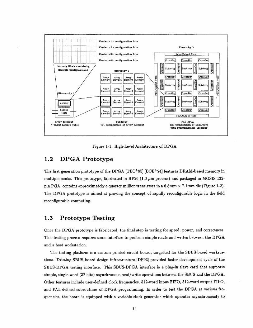
Figure 1-1: High-Level Architecture of DPGA
1.2 DPGA Prototype
The first generation prototype of the DPGA [TEC+95] [BCE+94] features DRAM-based memory in
multiple banks. This prototype, fabricated in HP26 (1.0 pm process) and packaged in MOSIS 132-
pin PGA, contains approximately a quarter million transistors in a 6.8mm x 7.1mm die (Figure 1-2).
The DPGA prototype is aimed at proving the concept of rapidly reconfigurable logic in the field
reconfigurable computing.
1.3 Prototype Testing
Once the DPGA prototype is fabricated, the final step is testing for speed, power, and correctness.
This testing process requires some interface to perform simple reads and writes between the DPGA
and a host workstation.
The testing platform is a custom printed circuit board, targetted for the SBUS-based worksta-
tions. Existing SBUS board design infrastructure [DP93] provided faster development cycle of the
SBUS-DPGA testing interface. This SBUS-DPGA interface is a plug-in slave card that supports
simple, single-word (32 bits) asynchronous read/write operations between the SBUS and the DPGA.
Other features include user-defined clock frequencies, 512-word input FIFO, 512-word output FIFO,
and PAL-defined subroutines of DPGA programming. In order to test the DPGA at various fre-
quencies, the board is equipped with a variable clock generator which operates asynchronously to
Context< > configuration bits
Context<2> configuration bits Hierarchy 3
Context<3> configuration bits
Context<4> configuration bits
Array Element SubArray Full DPGA4-Input Lookup Table 4x4 composition of Array Element 3x3 Composition of SubArrays
with Programmable CrossBar
Hierarchy 2
Aray AraeAra:-~lAmen Eleent ElmnEeet
:Array Array Ara Ara
_ :Aen ElemetElmntEemn
ArrayA ra Arra Array

04 ~~i Al *,
I
I
I;I
I
I
I1
Figure 1-2: Die Photo of the DPGA Prototype

the SBUS.
1.4 Thesis Organization
This thesis summarizes the entire testing and debugging process of the DPGA prototype. It first
characterizes the hardware built, describes the software written for interfacing test vectors, reports
the results from the DPGA silicon, and finally concludes with the lessons learned from the overall
DPGA development as well speculations on current technology and commercial trends.

Chapter 2
Hardware
The main purpose of the SBUS-DPGA interface board is to transfer data between the host (user)
and the DPGA. To simplify design and implementation, the board is implemented as a slave device
supporting only single word transfers. All board functions are controlled by a finite state machine.
Useful documentation for SBUS application may be found in [Sun90O] and [Lyle92].
2.1 Development Tools
The development of the SBUS-DPGA printed circuit board was done on the existing Transit Canon-
ical Form (TCF) infrastructure [SD93]. TCF is a LISP-like front-end language which facilitates logic
synthesis and simulation through a variety of tools. Logic simulation was done using Verilog (Ca-
dence's Verilog-XL) with Logic Modeling (Synopsis's Logic Simulation library). The SBUS Verilog
simulation model, provided by Sun, greatly facilitated the design and verification processes. The
printed circuit board was placed and routed using the Allegro tools. The PCB was fabricated by
Multek through MOSIS with six layers of metal in 6-mil pitch. These six layers of metal are: top,
intermediate top, power, ground, intermediate bottom, and bottom.
2.2 Architecture
The SBUS-DPGA interface consists of four modules: the transceiver I/O latch, finite state machine
(FSM), variable clock generator, input/output DPGA FIFO, and DPGA control logic. In order
to minimize hardware complexity, all reads and writes are kept to single-word operations. Neither
extended nor burst-mode operations are supported. Figure 2-1 describes the high-level architecture
and data-flow.

Figure 2-1: Architecture of SBUS-DPGA Interface
18

2.2.1 Synchronization
To test the DPGA at various clock frequencies, the SBUS-DPGA board must provide its own
variable clock generator for the DPGA since it can't rely on SBUS's fixed clock of 25 MHz. Having
this variable clock feature requires additional mechanism to support asynchronous transfer protocols
between the SBUS and the DPGA. The board uses one of the most straight-forward asynchronous
protocols, the READY/ACKNOWLEDGE handshaking.
The asynchronous handshaking mechanism uses four cascaded registers to buffer signals between
producer (SBUS) and consumer (DPGA). When the SBUS has data for the DPGA, it asserts the
signal DATA AVAILABLE until the receipt is acknowledged (DATA ACKNOWLEDGED) by the DPGA.
This DATA AVAILABLE signal is registered twice in consecutive DPGA clock cycles to ensure a non-
glitching signal by the end of the two DPGA cycles. Once synchronized to the DPGA clock, the
latched assertion can be fed cleanly into the DPGA. The DPGA then acknowledges the receipt of
the data by registering it in two consecutive SBUS clock cycles. This causes the original DATA
AVAILABLE to deassert.
2.2.2 Memory Operations
A write operation into DPGA's context memory could be accomplished in one DPGA cycle, as
long as the SBUS keeps the data asserted during that DPGA cycle. This is easily satisfied as
multiple SBUS cycles are always longer than the one DPGA cycle. However, a read operation is less
straightforward. The SBUS read operation requires the data be written out to the bus in exactly one
cycle. Furthermore, SBUS demands all data and control signals must be tri-stated in the subsequent
cycle.
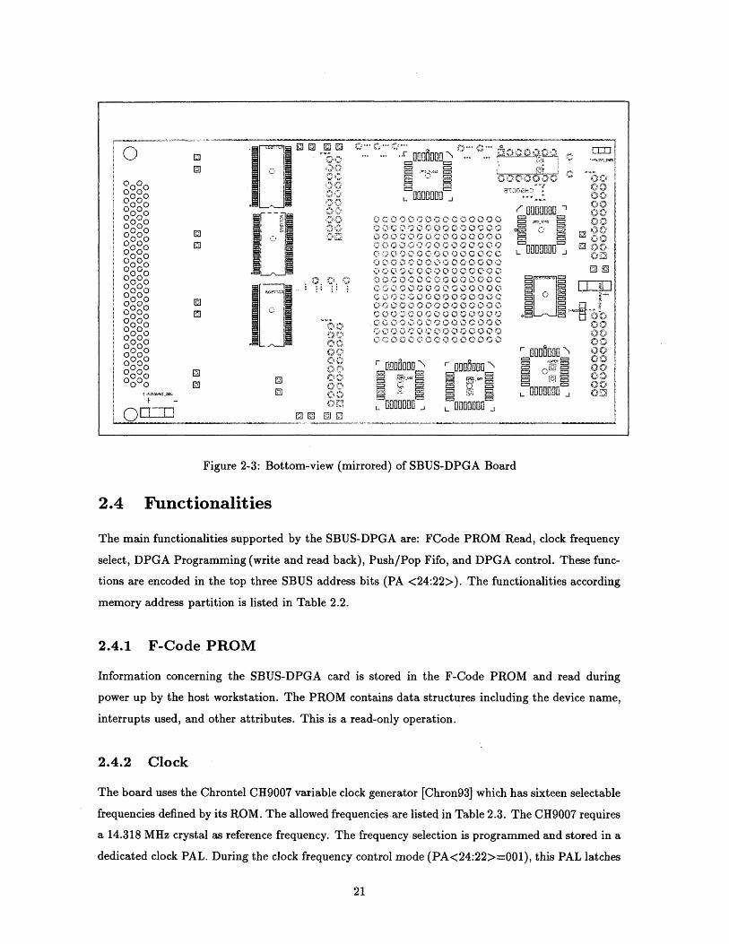
2.3 Board and Components
The SBUS-DPGA board has a relatively large number of logic components for its size. A total of ten
56-pin, shrink small-outline 300-mil packages (DL), five PLCC28 PALs, four HP debugging pods,
one PGA132 SOIC, along with others parts including clock, PROM, and SBUS connector. Table 2.1
lists the board components and Figures 2-2 and 2-3 show the board placements.
The dimension specification of the SBUS Single-Width card is 83.82 mm x 146.7 mm. Given this
dimension, the board doesn't have enough real estate to host all the aforementioned components on
only one side. The board design takes advantage of the fact that the majority of the components
used are surface-mounts, which made dual-side assembly a logical solution. This approach practically
doubles the board packing density for surface-mount devices. More importantly, the 48-bit bus of the
two sets of FIFOs line up when placed one on the opposite side of the one another. They efficiently
share input/output buses and significantly reduce the wires needed for routing.

Table 2.1: SBUS-DPGA Board Components
-0( 0() F::
(- '<
7O1Qi
0
S00 **C,00 0 0- oooo
0< ý ,< CA, 0 : 0 : 0 : 0 0 l,4A,;
0i 0 0 Ci0 0 00 , 0 0 0 001
ft000000000000000:01 000000 000000001o00©000000 o 000 0 o 0 o
0::0 0 0 © 0 0 0 © 0 © 0 <0 0 C"idioooooaoooooooooi
o~ooooooaooooooooaiaaa EQ MEoCoo
C E E E E F-'00(½)) F-C EEO CE CE OOOO
Ci Q F- OOOO
ooLn0 0tI
i •O0
- HP PO
i ) I,'-
( ''Cl
] -
0 0<>
00±0000
Figure 2-2: Top-view of SBUS-DPGA Board
Component Device Package QTYTransceiver ABT116501 SOIC56 418-bit FIFO ACT7803 SOIC56 6
Debugging Pods HP PODS HEADER10X2HP 4F-Code ROM 27256 PLCC32 1
FSM PAL 22v10 PLCC28 5DPGA DPGA PGA255 1
EQ000 i0
D00
o O00<o>oc3
0±<0S0 o0 C0o <1000C
0,.00 C00
oOc00.0 ,0
[iLI ii*nfB]I
OOLS00
o0000I 0@o0[8_(I
o [ ;1
oo00 0
00
on
lp Pk,
10 1I! I1ea
- il_,lW°U=:
000 ooo o0 00 00 00 0
o o0 0o o
0 0o oO o0 00 0
0 00 0o 0
OO0000 •.0.0
0o 0000000
0 0 0 00 000
G 0C77 ""M '"O "" .• -
L D00b000I .
c. 00,00000 00000C" co ýo -cooocoCoo
0 1 00000 00000000 C©00000000000Q0
000e00000000000a ©.0 0 Q000000000 00 10
i I: a 000' OOOO00 0000
00000~Q0000000-0 0000 QOOO O0000
0000000000 t
L 00Boor .j L 0000000 .flffll F flllifff= f~r=, 3~·
= a 1= ==~ = =3T~iSC
Jrffllll i. nnnnoZ i
Figure 2-3: Bottom-view (mirrored) of SBUS-DPGA Board
2.4 Functionalities
The main functionalities supported by the SBUS-DPGA are: FCode PROM Read, clock frequency
select, DPGA Programming (write and read back), Push/Pop Fifo, and DPGA control. These func-
tions are encoded in the top three SBUS address bits (PA <24:22>). The functionalities according
memory address partition is listed in Table 2.2.
2.4.1 F-Code PROM
Information concerning the SBUS-DPGA card is stored in the F-Code PROM and read during
power up by the host workstation. The PROM contains data structures including the device name,
interrupts used, and other attributes. This is a read-only operation.
2.4.2 Clock
The board uses the Chrontel CH9007 variable clock generator [Chron93] which has sixteen selectable
frequencies defined by its ROM. The allowed frequencies are listed in Table 2.3. The CH9007 requires
a 14.318 MHz crystal as reference frequency. The frequency selection is programmed and stored in a
dedicated clock PAL. During the clock frequency control mode (PA<24:22>=001), this PAL latches
0 Cr iO©
©•i~
-
FIiIL]
.
"~~""'~""'"~ ~ ~'~''''~"""'~~'~~'~'"""""'~~"'~~`~
r u 00
o ,.,.'." 0 co
noS008000= =00
F o
S,-. OE= o,.-- ,.l, _ © ©rrr %,$a.•
jBOO
9VO
a

C4 Q 6 20 ;Q;A DU
tie i t
Ul~lll S1 b1 "
ii iiii or to 01 Op 0111'ý.fl i
I!' .. .... .....
I 'M' SSPý I WJSJIIN "1111 --- 01I~A I f.'~tP -1.-H 1l. k I... ... ....-
R tlffl 2j.®R rILLI;.-M Itlý` I- - AWPW\ý I !, ION -ýi' 'M MEWMP L I I JSVU LCZ7 M: M I I T N_P16 W"AW AIP WIMP,W till 'FM Ailrli;1111W'Qt"ý
N i
i' ......
2 II.. " • . . .. . . ~ ~ ~.. ..... .. } ' i iii ii • ij
U ! El C -----I <
Figure 2-4: Composite-view of SBUS-DPGA Board
(N
LC:( C~
C.
ir..... ....H0 UU1H Ut Il~~r(F I------------- ..... ...z=t;
i n
I N li.. .... . .. .... .Igo, trotii i i inii H--- ---- ----- --- -- --- -- --- --... ... .. ... .-- ------ ------------ ----- ------ -------. ...........------- ..............rigiJ. S ii ... --A........
KO-El...... ........
--------- ---...... ...... r
ay..... ... ....... ii~tii# ~ Is
; 6M
L.-..-\M·--·-- ··- ·····
~~~hYEi Hl 7%~fh~ 7ii ii av vii~a ~n~Bh\~n~arn ~

Memory PartitionPA<24:22> DPGA Function
000 F-Code PROM001 Clock Frequency Control010 Programming Lines011100 FIFO <31:0>101 FIFO <47:32>110 DPGA Control111
Table 2.2: SBUS-DPGA Physical Memory Address Partition
D<3:0> Frequency D<3:0> Frequency0000 16.0 1000 8.00001 40.0 1001 20.00010 50.0 1010 25.00011 80.0 1011 40.00100 66.6 1100 33.30101 100.0 1101 50.00110 80.0 1110 4.00111 4.0 1111 2.0
Table 2.3: Chrontel CH9007 Clock Frequency Table (in MHz)
in the 4 LSB from the data bus. At all other time, the PAL asserts those 4 LSB as latched previously.
2.4.3 Context Configuration
The configuration memory of the DPGA is programmed via a dedicated 32-bit programming bus.
The the memory bits could also be read back for debugging purposes. This context memory read
back functionality proves to be essential in the actual debugging process.
The read and write operations of the DPGA require somewhat different implementations. For
the write operation, the SBUS asserts both the address and data buses for the entire duration
of the write. The DATA AVAILABLE signal is propagated to the DPGA. Subsequently, the DPGA
PROGRAM OPERATION (ProgOp) is asserted for exactly one DPGA cycle. This is when the data is
actually written to the DPGA. The acknowledgment follows and the SBUS address and data lines
are released. For the read operation, the SBUS asserts the address bus for the DPGA. Signaled
by DATA AVAILABLE, the DPGA PROGRAM OPERATION stays asserted until the acknowledgment is
propagated back to the SBUS. The ProgOp signal is combinational (rather than DPGA-registered)
because the data bus needs to be released immediately after the SBUS acknowledgment in order
prevent contention with the subsequent SBUS operation.
2.4.4 Input/Output FIFO
One of the board's design goal is to allow the DPGA to operate at various clock frequencies. Since
the SBUS is running at a fixed rate of 25 MHz, it must transfer data to the DPGA asynchronously.
The DATA READY/ACKNOWLEDGE handshaking mechanism is a straight forward protocol for asyn-
chronous transfer. This protocol, used by DPGA context configuration, takes several cycles to
complete one single transfer due to propagation of the ready and acknowledge signals. However, high-
bandwidth data-flow for the DPGA is desired, meaning the DPGA should be able to input/output
word in consecutive clock cycles (burst transfers). To achieve this design goal, FIFOs are used to
buffer input and output data.
The asynchronous FIFOs (7803) are the ideal choice because they have dedicated 18-bit wide
buses for input and output. Synchronization between the two clocks is handled internally by the
7803. With 48-bit wide data I/O, the DPGA transfers data using three FIFOs parallel as input
buffer and three FIFOs as output buffer. Two bits from all six FIFOs are not used.
Pushing data on the DPGA's 48-bit input FIFO requires only one write cycle. It combines both
the 32-bit of the data bus and 16-LSB of the physical address bits into a single 48-bit write operation.
Popping data off the DPGA's output FIFO requires two operations, one pop for the bits <31:0>
and another for the bits <47:32>.
The FIFOs are controlled by the DPGA Control PAL. The PAL could independently assert three
READ ENABLE (pop) signals on the input FIFOs as well as two WRITE ENABLE (push) signals on
the output FIFOs. The other control signals include DPGA context bits and CONTEXT STROBE.
The inputs of the PAL include a ready bit of input FIFO, 6 bits of SBUS data, and 4 bits of feedback
bits from DPGA's programmable IO. This gives the PAL-implemented FSM full control of run-time
context-switching independent of the SBUS as well as a maximum I/O bandwidth of 48 bits per
DPGA cycle. Since 4 bits of DPGA programmable IO are fed back to the PAL, the DPGA could
control the FSM with its own internal configurable logic. Figure 2-5 shows the interface between
the DPGA and its input and output FIFOs.
2.4.5 DPGA Control and FSM
A 22v10 PAL is dedicated to implement externally the control/FSM for DPGA. This allows on-board
control of the DPGA without the overhead of going through the SBUS. Such is especially desirable
in situations requiring rapid context switching on a cycle-time basis as well as high data bandwidth
(burst mode) between the DPGA and the Input/Output FIFOs.
The DPGA control PAL takes 3-bit opcodes as program select input from the SBUS. The PAL
could be programmed to assert DPGA signals (CTX_STROBE, CTXADDR) as well as FIFO signals
(RDEN (input), WREN (output). The PAL output also includes 4 I/O bits to the DPGA which

512x
512x
512x
In
8 FIFO (7803)
8 FIFO (7803)
8 FIFO (7803)
)ut Fifos
Figure 2-5: Input and Output FIFO of SBUS-DPGA Interface
A AAA
-~~- V V V
00) L L _
CD: 0 0 0
DPGA

Table 2.4: DPGA Control PAL opcodes
enables DPGA's programmable logic to be part of the data control. These four bits also serve as
state bits or counters which allow each opcode to have up to 16 states.
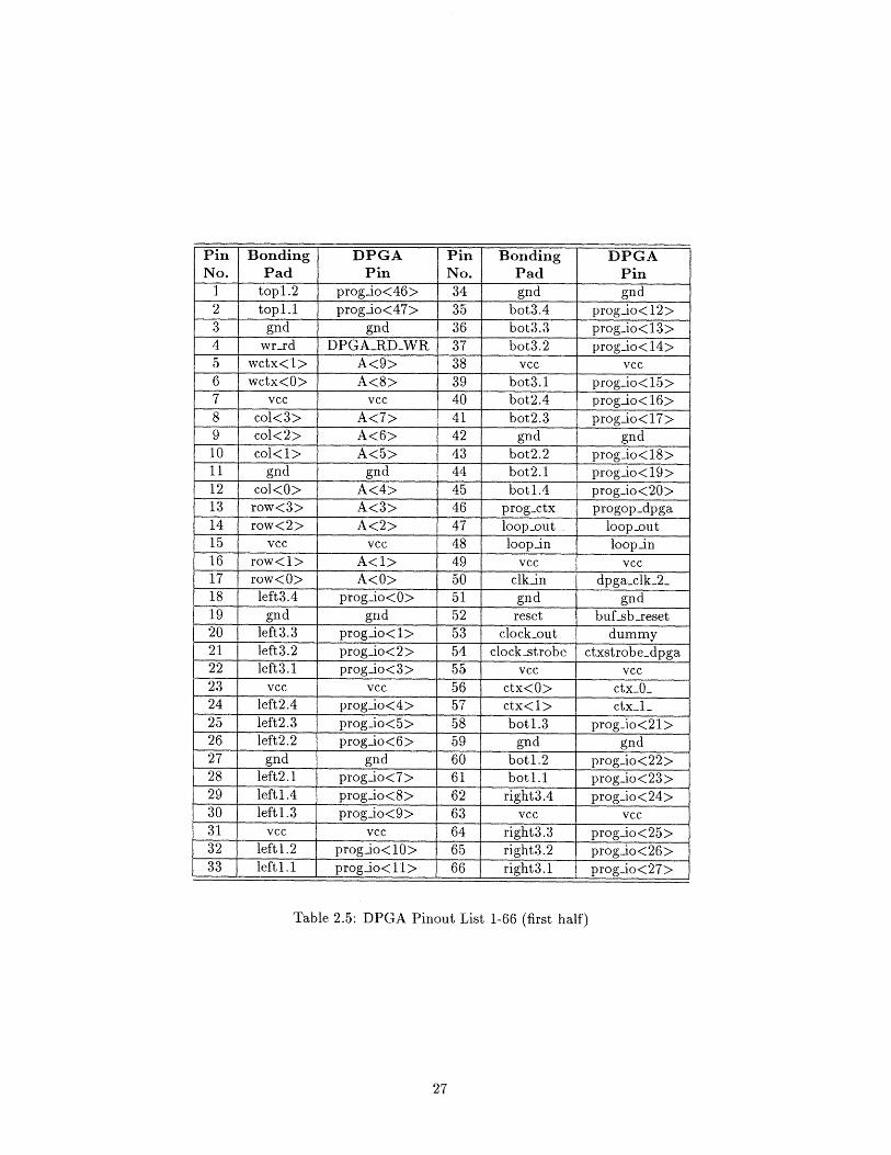
2.4.6 DPGA Pinout
The DPGA is in a PGA132 package, hosted by a ZIF225 (zero-insertion force) socket. The pinout
is listed in Tables 2.5 and 2.6.
2.4.7 Debugging Pods
To facilitate debugging of the test board, four HP Pods make bus and control signals accessible to
the HP logic analyzer. Pod 1 is connected to exclusively DPGA control signals and its input/output
FIFO controls. Pod 2 is connected to SBUS control signals which include the lower-order address
byte as SBUS Address Strobe (SBAS), SBUS Select (SB.SEL), SBUS Read (SBRD), SBUS
Acknowledge (SB_ACK<0>), and transceiver enable signals. Pods 3 and 4 are connected to the
32-bit data bus of the SBUS.
OpCode State Remark000 Idle All outputs are de-asserted001 Unused User-programmable010 Unused User-programmable011 Unused User-programmable100 Unused User-programmable101 Run FSM Start FSM counter110 Context Strobe Strobe the context given by SBUS111 Fifo Test Performs a FIFO Write-Through Test
(Pops a value off input FIFO and pushesit onto the output FIFO)
Pin Bonding DPGA Pin Bonding DPGANo. Pad Pin No. Pad Pin
1 topl.2 prog-io<46> 34 gnd gnd2 top l.1 progio<47> 35 bot3.4 progio<12>3 gnd gnd 36 bot3.3 prog_io<13>4 wr-rd DPGA_RDWR 37 bot3.2 prog-io<14>5 wctx<1> A<9> 38 vcc vcC6 wctx<0> A<8> 39 bot3.1 prog-io<15>7 vcc vcc 40 bot2.4 prog-io<16>8 col<3> A<7> 41 bot2.3 progio<17>9 col<2> A<6> 42 gnd gnd10 col<1> A<5> 43 bot2.2 prog-io<18>11 gnd gnd 44 bot2.1 prog-io<19>12 col<0> A<4> 45 botl.4 progio<20>13 row<3> A<3> 46 progctx progop_dpga14 row<2> A<2> 47 loopout loopout15 vcc vcc 48 loopin loopin16 row<1> A<1> 49 vcc vcc17 row<0> A<0> 50 clkin dpga_clk_2_18 left3.4 prog-io<0> 51 gnd gnd19 gnd gnd 52 reset bufsb.reset20 left3.3 prog.io<l> 53 clock_out dummy21 left3.2 progio<2> 54 clock-strobe ctxstrobe'dpga22 left3.1 progio<3> 55 vcc vcc23 vcc vcc 56 ctx<0> ctx_0_24 left2.4 progio<4> 57 ctx<1> ctx_l_25 left2.3 progio<5> 58 bot 1l.3 prog-io<21>26 left2.2 prog-io<6> 59 gnd gnd27 gnd gnd 60 botl.2 prog.io<22>28 left2.1 prog-io<7> 61 botl.1 prog-io<23>29 leftl.4 prog_io<8> 62 right3.4 progio<24>30 leftl.3 progio<9> 63 vcc vcc31 vcc vcc 64 right3.3 progio<25>32 leftl.2 prog-io<10> 65 right3.2 progio<26>33 leftl.1 prog-io<11> 66 right3.1 progio<27>
Table 2.5: DPGA Pinout List 1-66 (first half)

rin I INo.
PinNo.676869707172737475767778798081828384858687888990919293949596979899
BondingPad
right2.4right2.3
gndright2.2right2.1rightl.4
vcc
right1.3rightl.2right1.1
gndprog<31>prog<30>prog<29>
vccprog<28>prog<27>prog<26>
gndprog<25>prog<24>prog<23>
vccprog<22>prog<21>prog<20>
gndprog<19>prog<18>prog<17>
vccprog<16>
progio<28>prog-io<29>
gndprog-io<30>prog-io<31>progio<32>
vcc
progio<33>prog-io<34>progio<35>
gnd
d<1>d<l>d<2>
vccd<3>d<4>d<5>
gndd<6>d<7>d<8>
vccd<9>
d<10>d<ll>
gndd<12>d<13>d<14>
vccd<15>
100101102103104105106107108109110111112113114115116117118119120121122123124125126127128129130131132
Table 2.6: DPGA Pinout List 67-132 (second half)
DPGA Pin Bonding DPGAP'ad
prog<14>gnd
prog<13>prog<12>prog<11>prog<10>
vcc
prog<9>prog<8>prog<7>
gndprog<6>prog<5>prog<4>
vccprog<3>prog<2>prog< 1>
gndprog<0>
top3.4top3.3
vcctop3.2top3.1top2.4
gndtop2.3top2.2top2.1
vcctopl.4topl.3
I __IL[f 1
prog<15> d<16>
Pind<17>d<18>
gndd<19>d<20>d<21>
vccd<22>d<23>d<24>
gndd<25>d<26>d<27>
vccd<28>d<29>d<30>
gndd<31>
prog-io<36>prog-io<37>
vccprog-io<38>prog-io<39>progio<40>
gndprogio<41>progio<42>progio<43>
vccprog-io<44>progio<45>
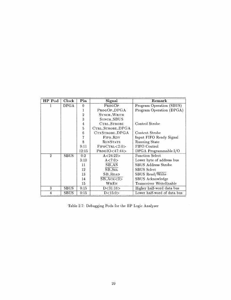
HP Pod Clock Pin Signal Remark1 DPGA 0 PROGOP Program Operation (SBUS)
1 PROGOP_DPGA Program Operation (DPGA)2 SYNCH_WRITE3 SYNCHSBUS4 CTRL_STROBE Control Strobe5 CTRLSTROBEDPGA6 CTXSTROBEDPGA Context Strobe7 FIFO_RDY Input FIFO Ready Signal8 RUNSTATE Running State
9:11 FIFOCTRL<2:0> FIFO Control12:15 PROGIO<47:44> DPGA Programmable I/O
2 SBUS 0:2 A<24:22> Function Select3:10 A<7:0> Lower byte of address bus
11 SBAS SBUS Address Strobe12 SBSEL SBUS Select13 SBREAD SBUS Read/Write14 SB_AcK<0> SBUS Acknowledge15 WREN Transceiver WriteEnable
3 SBUS 0:15 D<31:16> Higher half-word data bus4 SBUS 0:15 D<15:0> Lower half-word of data bus
Table 2.7: Debugging Pods for the HP Logic Analyzer

Chapter 3
Software
The testing software used for the SBUS-DPGA interface is built upon the Transit infrastructure.
The low-level device drivers to read and writes on the SBUS interface were already implemented
from a previous project which used similar read/write operations.
3.1 Optimization
A few modifications were made to improve performance operations requiring multiple SBUS reads/writes.
The software communicates with the SBUS through a memory map (mmap) operation. Each mmap call
is an operating system function that establishes a mapping between the process's physical address
space to the virtual address. This is a relatively expensive function call in terms of computational
cycles. Invoking mmap call during initialization rather than during each read/write operation sig-
nificantly cuts down the unnecessary overhead of repeated memory maps. Consequently, this small
optimization greatly accelerates functions with successive SBUS reads or writes.
3.2 Clock
Using the Chrontel CH9007b part, the board can clock the DPGA at one of the sixteen pre-defined
frequencies listed in Table 2.3. The 4 LSB of a simple write within the physical address partition at
PA <24:22>= 001 will be latched in the clock control PAL which changes DPGA's clock frequency.
The corresponding clock frequencies are listed in Table 2.3 according to their frequency code.
Usage: setclk frequency-code where frequency-code is in hexadecimal
3.3 FIFO
3.3.1 Single Push/Pop
The following commands could be used at shell-prompt to manually test the basic FIFO functions.
The three input FIFOs could receive a 48-bit value from a single push off the SBUS (32-bit data and
16-bit address). The three output FIFOs has to output two values separately (32-bit and 16-bit).
A useful test for the two sets of FIFOs is write_thrufifo which pops a 48-bit value from (A) and
pushes it into (B). Consult Figure 2-5 for the interface of the FIFOs.
Usage: pushIifo value where value is 48-bit hexadecimal
Usage: popifo returns 32-bit value from FIFOs 1 and 2
Usage: pop_.ifo2 returns 16-bit values from FIFO 3
Usage: writethrufifo pops a value from the input FIFO and pushes it to the output FIFO
3.3.2 Comprehensive Test
To fully test the FIFOs, a utility, fifotest automated a sequence of 512 consecutive pushes into
the input FIFOs, followed by 512 writethru.fifo, and a sequence of 512 pops from the output
FIFOs. If all these 512 output values correspond to those written in, the FIFO test succeeds. It
should be noted that this test will work only if the DPGA has its programmable I/O in tristate
mode. In the case where the I/O's are not tristatable, the DPGA should be removed from the socket
in order to run this test. Should contention occur, DPGA dominates and overwrites the values of
the input FIFO.
Usage: fifo_test
3.4 Memory
3.4.1 Single Read/Write
Values of the DPGA memory could be accessed through individual read/write.
Usage: memwrite row column context value where row and column are 4-bit, context is 2-bit,
and value is 32-bit hexadecimal
Usage: memread row column context returns 32-bit value from specified row, column, and context
3.4.2 Memory Lossage Report
The program map.memory. c generated a semi-comprehensive report of how memory retains its values
over time. To account for possible values illegitimately read due to capacitance, the test executes
a sequence of two writes and a read. First, it writes the value of the test vector, followed by the

Function Command Parameter(s) NoteClock set_clk freq-code freq-code (0-F) correspond
to those shown in Table 2.3FIFO pushfifo value value is 48-bit hex
pop.fifo return value is 32-bit hexpop-.ifo2 return value is 16-bit hex
write-thru.fifoMemory mem_write row column context value value is 32-bit hex
mem.read row column context return value is 32-bit hexmscrub3
Table 3.1: Test Software Summary
inverse of the test vector (to overwrite the previous value retained by mere board capacitance),
followed by a read back. If read back succeeds in that sequence, then it is classified as "All OK"
(both read/write pass over a period of 10's milliseconds). It then repeats reading sequences over
a specified period of time intervals and checks for decay. It dumps out the bit difference between
each successive rounds. The number of rounds and delta time interval can all be specified in the
definition of mscrub2. c. If no bits decay in a single memory block over all the rounds, the block
column and row will be reported as "perfect" in the last stage. The variables are easily adjustable
to perform more comprehensive tests over a variety of time intervals, clock frequencies, and etc.

Chapter 4
Results
4.1 Board Assembly
Once fabricated, the printed circuit board was assembled and soldered by hand. Sockets (PLCC28)
were installed to facilitate the removal and re-insertion of the five PALs.
The PLCC28 sockets were responsible for much of the earlier board flakiness. Made of plastic,
the surface-mount sockets were somewhat difficult to installed with a heat gun because they were
easy to melt. If heated for too long, the plastic frame will start to deform. If not heated long enough,
the solder glue won't melt and make robust solder pin connections. The: dilemma is that the optimal
lengths in time for heat exposure don't converge for both. Flaky connections were made early as
a consequence of very tentative soldering. Experience proves soldering guns with direct contact, as
opposed to air-heated guns, were much more effective and robust in plastic PLCC28 socket assembly.
Photos of the assembled printed circuit board is shown in Figures 4-1 (top side) and Figure 4-2
(bottom side).
4.2 Pads
The pads used by the DPGA were taken from another project, Abacus, in which the pads have been
proven to work. However, the logic control for the pads have been modified for the needs of the
DPGA. Two major flaws with the I/O pads of the DPGA surfaced in the testing process. These
two flaws were due to oversight and the lack of thorough layout verification.
The control logic of the 48-bit programmable I/O includes a "reset" mode that should force the
pads to be in tristate mode. Its purpose is to prevent contention during situations with unpredictable
pad configurations such as power-up. However, in the layout implementation, a transistor within the
pad control has its drain floating instead of connecting to ground. In addition, one of the logic gate

Figure 4-1: Photo of assembled SBUS-DPGA PC board (top view)
36
- I I-- I~ -- "-~ - -~--~-~I~

Figure 4-2: Photo of assembled SBUS-DPGA PC board (bottom view)
I
- ~~I-~~-~~-~~-`~~-`~-~II-~-~-~--- n ~-`-~ ~I--`-`-I-~-~~" ~1~~'-~-"I

of the control was mistakenly implemented as a NAND gate rather than an NOR gate. This forces
the pads to be constantly driving. Consequently, the programmable I/O pads are always output
enabled, even during reset mode. This flaw is isolated to the 48-bit programmable data I/O, so the
32-bit context programming I/O are not affected.
4.3 Memory
Memory of the DPGA is implemented using a 3-transistor DRAM technology (Figure 4-3. The
prototype memory suffers from flaws that appeared at first to resemble leakage. However, this
memory flaw is more subtle than plain leakage. The problem has to do with timing issues on the
memory control logic signals. As the first DRAM-based field programmable gate array, the DPGA
took a calculated risk in building dynamic memory cells.
Though denser, DRAM cells are are less robust than traditional static memory cells because of
their added complexity of refresh logic as well as leakage and timing issues. In addition, the DRAM
choice seems logical because the overhead of the refresh logic is amortized over the multiple banks
of memory. These issues, combined with the lack of VLSI experience, proved to be the ultimate
weakness in the DPGA prototype.
4.3.1 Refresh Logic
There is repeatable evidence that refresh is working properly (for those memory that have been
verified not to leak). This is observed through the context strobe signal (CTX.TOGGLE). When
CTX.STROBE is constantly asserted on context 0 (refreshing exclusively context zero), only the value
of that context remains valid. The three other contexts all decay to zero almost immediately. This
behavior confirms the refresh logic functionality. There is one minor subtlety when conducting this
test. When the CTX.STROBE is asserted during a memory read, the value read out is that of the
context been strobed (CTXADDR), not the context set by the programming context (PROG.CTX).
This reflects the proper behavior as a constant refresh of context 0 also drives out to the programming
lines.
4.3.2 Board Capacitance
One interesting observation was made concerning the data bus and the debugging pods. It appears
that there is enough capacitance on the floating data bus of the board to store values for several
seconds, even if the DPGA chip isn't physically plugged in. However, this observation is true only
when the debugging pods are not plugged in. When they are, the added impedance of the HP Pods
changes the behavior of the floating data bus.

Context<1Context<2Context<3Context<4
32-Column by 4-ContextMemory Block
re<O>
re<1>
re<2>
re<3>
4-m1L iviemoryColumn
Figure 4-3: Memory of DPGA
4.3.3 PAL Internal Pull-Ups
The 22v10 PALs used, GAL22v10B 15LJ from Lattice, have internal pull-ups in its inputs. This
should be noted in debugging process because the SBUS data bus, connected to PAL inputs, may
appear to drive out misleading values when the bus is actually in tristate mode.
4.3.4 Timing Problems
The flaw observed in the DPGA memory can be attributed to one theory. This theory claims that
the timing delay due to long wires and large capacitive loads between memory cells and their refresh
logic causes ill-timed assertion of control signals.
All the cells and refresh logic of the DPGA memory are composed with the same design, irre-
spective of the distance between them. This poses a problem when the cell and its refresh logic are
far apart, thereby introducing timing delay in the refresh control signals. From Figure 4-3, it can be
seen that if the signal IWE (internal write enable) is delayed in turning off while a RE signal is starting
to assert, then the stored value will be illegitimately written over by the value of a non-corresponding
DRAM cell. This leads to stored values to be written over with "junk" values, rather than "decaying
away" as in simple leakage. Since the DRAM cells require constant refresh, any untimely assertion
of refresh signals will result in adverse consequences for memory cell's retention. This is the nature
of dynamic memory and is a trade-off for its higher density.
4.4 DPGA Control Logic
4.4.1 Read/Write Signal
To write into the DPGA context memory, one needs to assert the ProgOp (Program Operation)
signal while pulling the Read/Write signal low. To read back the context memory, one does the
same except pulling the Read/Write signal high. This works as documented. However, it should
also be noted that the read/write signal should default read (high). Having a read as default will
avoid overwriting values into DPGA and trashing valid memory bits, particularly in the case when
ProgOp is not asserted. In the early debugging stage when the Read/Write signal defaulted to write,
spurious writes took place and was mistakenly interpreted as memory leakage.
When a read comes along, DPGAR.DWR goes high in the same DPGA cycle that prog_op be-
comes low. If these are both sampled synchronously and timed the same, no problem should occur.
However, if there's any chance that the earlier value of DPGAIRDWR (still asserting write) is seen
as soon as PROGOP is asserted, then a false write during read operations.

4.4.2 Context Strobe Signal
Reads and context strobe should not happen at the same time. If the read and the context strobe
happen to be using the same cell, then things might work - but the charge sharing may leave the
memory charge near threshold so that decay happens quickly. Context strobe is a negative asserted
signal - it forces a refresh of the context specified by CTx<1:0>, then returns to the count. A
"manual" refresh could be achieved using this method.


Chapter 5
Conclusion
The DPGA development and testing efforts have led to many profound observations. One of the
underlying themes of the DPGA was resource re-utilization. By incorporating additional memory
on chip, the DPGA tries to reuse the logic blocks with extra configurations in order to obtain more
functionalities. This resource re-utilization approach is fundamentally sound. However, it turns out
logic blocks occupy only a small portion of the silicon real estate when compared relative to the
interconnect. This observation leads to applying the same approach to other resources.
5.1 DPGA Offsprings
Two second-generation projects have evolved from the original DPGA development. One is Time-
Switched FPGA (TSFPGA) [Chen96a] and the other is MATRIX [MD96]. The TSFPGA takes
resource utilization one step further by multiplexing the interconnect resources over time (thereby
time-switched FPGA). Thesis work on the TSFPGA is done by Derrick Chen in in [Chen96b].
Matrix is a coarse-grain programmable logic which supports configurable instruction distribution
and deployable resources. Thesis work on the Matrix is done by Ethan Mirsky in in [Mir96b].
Building upon the lessons and experience gained from the original DPGA development, these two
second-generation projects explore new programmable device architectures that aim to reap the
most advantage of computational resources through re-utilization.
5.1.1 Time-Switched FPGA
TSFPGA [Chen96b] is a variation of the original DPGA. It too tries to utilize the silicon resources.
However, one of the unexpected conclusions of DPGA's VLSI analysis shows that silicon area is dom-
inated by interconnect, not logic elements nor memory. This implies re-utilization of the interconnect
rather than the logic elements will achieve greater utility of the overall silicon area.

By pipelining the switching operations and adding a modest amount of context memory in the
interconnect, the TSFPGA reuses the limited interconnect switches and wires in time. As a result,
more effective switching capacity is achieved with less physical interconnect. With sufficient context
memory, time switching makes the task of finding a functional route trivial. Consequently, large
parts can be routed in seconds when quick mapping is desirable, while slower mappings can be used
to achieve high performance operation [CD96].
5.1.2 Matrix
MATRIX is coarse-grain, reconfigurable computing architecture which supports configurable in-
struction distribution. Each logic element (BFU: Basic Logic Unit) features an 8-bit ALU with
fully programmable control logic and data-paths. Device resources are allocated to controlling and
describing the computation on a per task basis. Application-specific regularity allows us to com-
press the resources allocated to instruction control and distribution, in many situations yielding
more resources for data-paths and computations. The adaptability is made possible by a multi-level
configuration scheme, a unified configurable network supporting both data-paths and instruction
distribution, and a coarse-grained building block which can serve as an instruction store, a memory
element, or a computational element.
Matrix is an excellent candidate for digital signal processing applications because each logic
element has embedded ALU that excels in multiply-accumulate. Traditional fine-grain architectures
such as FPGAs suffer from low computational density (measured in bit operations per lambda
squared) because multiply-accumulators are costly to implement using fine-grain logic.
5.1.3 Future Projects
A third hybrid architecture combines both TSFPGA and Matrix. This hybrid architecture features
fine-grain logic embedded within coarse-grain logic blocks.
Ultimately, a TSFPGA/Matrix-coupled microprocessor [DeH94] is the computational substrate
of choice that will combine the advantages of fixed-hardware as well as reconfigurable components.
5.2 Technology Trends
The current generation of field programmable gate array expends a large portion of its silicon area
in interconnect. Of the entire die area, only a small fraction of the silicon actually goes into the
logic and memory components as shown in the DPGA [BCE+94]. This observation seems to be
consistent with commercial programmable devices as well. It should also be pointed out that the
current generation of programmable devices are fabricated in processes with a small number of metal
layers (three or less). In order to provide sufficient routing, the interconnect does indeed dominate

Time Fabrication Programming LogicProject Frame Process Technology ElementDPGA 1995 HP26 (1.0 pm) DRAM 4-LUT
TSFPGA 1996 HP14 (0.5 pm) SRAM 4-LUTMatrix 1996 HP14 (0.5 pim) SRAM 8-bit ALU (add/multiply)
XOR planeTSFPGA-Matrix Future ? ?
DPGA-Microprocessor Future ? ?
Table 5.1: DPGA Projects
for most programmable devices using the current generation of fabrication processes. This is largely
due to system interconnect overhead as required by power, ground, and clock distribution.
However, significant fabrication process improvements are imminent. Within a few (3-5) years,
commodity fabrication processes will typically feature 5-8 layers of metal with 10+ layers in the
decade to come. The larger number of metal layers supported by future processes will fundamen-
tally change the design trade-offs of reprogrammable devices. These devices will stand to benefit
significantly from additional layers of metal, facilitating larger fan-ins and fan-outs of the logic block
and improving routability. At the same time, more metal layers incur much less inactive silicon
area. Consequently, interconnect should pose a lesser occupant of silicon area relative to the logic
and memory elements. No longer a limited resource, interconnects will likely to cost less in terms of
silicon real estate.
5.3 Industry Trends
In the year 1996, programmable devices are still relatively confined to the prototyping capacity.
Large programmable devices vendors such as Xilinx and Altera do not anticipate significant com-
mercial potential for reconfigurable computing in the short-term and thus they are making relatively
minor efforts to push for its advancement. Reconfigurable computing will remain a small academic
niche until convincing "killer apps" running on a reconfigurable substrate can demonstrate the
advantage of such architectures. This is what it takes to change the industry's acceptance of fixed-
hardware computing.
While programmable devices vendors are slow to explore/exploit the potentials of reconfigurable
computing, DSP vendors are approaching from the other direction. Newer generations of DSP have
become much more flexible and rapidly reconfigurable. Pilkington Electronics offers DSP with an
architecture resembling closely to that of Matrix in its line of reconfigurable video DSP [C95].

Appendix A
Implementation Files
All data files are served on the fileserver, transit.ai.mit.edu (128.52.38.26), in their appropriate
directories.
* Board Description
1. Source Description: /home/tr/designs/sbdpga/tcf/sbdpga.tcf
2. Final PCB: /home/tr/designs/sbdpga/allegro/sbdpga..Iilms.brd
3. Artwork: /home/tr/designs/sbdpga/allegro/artwork/
- sbdtop. art (top signal)
- sbd itop. art (intermediate top signal)
- sbdvcc . art (power plane)
- sbd.gnd.art (ground plane)
- sbd.ibot. art (intermediate bottom signal)
- sbdbot. art (bottom signal)
- sbdismtop. art (solder mask top)
- sbd smbot. art (solder mask bottom)
* SBus Control PALs
1. Finite State Machine to handle SBUS read/write request and acknowledgement:
- /home/tr/designs/sbdpga/tcf/sbd.ctrll .pal
- /home/tr/designs/sbdpga/tcf/sbd.ctrl2.pal
2. Control for programming variable clock generator
- /home/tr/designs/sbdpga/tcf/clockctrl.pal
3. Control for programming DPGA and FIFO

- /home/tr/designs/sbdpga/tcf/dpga.ctrl.pal
4. Synchronization control for ready and acknowledgement signals
- /home/tr/designs/sbdpga/tcf/rdyack.pal
* Testing Software
1. SBUS-DPGA Board Test: /home/tr/designs/sbdpga/verilog/sbdpga.v
2. DPGA Verilog Model: /home/tr/designs/sbdpga/DPGA/DPGAtop. v
3. DPGA Debugging Software /home/tr/designs/sbdpga/src/
- Set Clock Frequency: set.clock.c
- Push 48-bit value into FIFO (In): push-fifo. c
- Pop LSB 32-bit value from FIFO (Out): pop-fifo. c
- Pop MSB 16-bit value from FIFO (Out): popfifo2. c
- Comprehensive FIFO Test: fifotest. c
- Comprehensive Memory Map Summary: map-memory. c

Appendix B
Printed Circuit Board Artwork
C.C.u
Figure B-l: SBUS-DPGA PC board (top)
0
C C
I_~_~_II~~~ ____;i_ ___ _ __~_i~~~___ ____ ~_ _I I _
_I
~

Figure B-2: SBUS-DPGA PC board (intermediate top)
51

Figure B-3: SBUS-DPGA PC board (intermediate bottom)
jlU
C:M O
(,
I·;i·;0 i~: "
i.;
i,
d 3^
/-77-- ,. ..... .... .C
C--'' .. .....• •. ..,. ... ..... ... ... ..... ..., ... .. ............ ...... ..- ... ... ... . -. . ,..
toA 0............••.. - . .-- -- ,k~~~~~~~~~~~j~~.. .... .............,$..• .......--'. •. .a = = . .......: • . • .
• • "•' ...... ........ . . .... : • - . • • ( . ........ "."- :
,-...... _............ ...... ......... = • • ......... i • ••. •'i .i• iJ '-. - - • ....... ..... I .._ _.. .. .... .. . ... .... ... .... .... .... ....... :.........
... .......... ...............,............. •"" .. .; .. .. ""\ - "o " ' " , 7 .:• j •--- . -• -- .... --- .! ;:- ... q .- --_• ".; ...i .. .. .. ...... .. .. ...- -... . . . , .
•t,'.i, ~ ~ ~ ~ ~ ~~~~ ~~~~~~ ....W'" .." .= - "-.• ." ,. -- ,,- C :J., . :'.--.----•i ~ ~ ~ ~ ~ ~ ~ ...... .. ..... .i T; .:.. ...i ._. .. .. . ......... . -.. ......... ...... ....... ". " '- " .....-... .. ._..:.. . .. ., .,. _ .
.....i.. ..... . . ".. ........ ..... ..". ..,- .... .. . ". .. ... , '.. "-. - c s ,-
,• ; ! i - I........... .. .. .. .............. '- ' ' = - •• ;..-• " .'.. I ' ..-IQ
ib.- =: .= =•. ...... -t --J -..7 ..... ... ..7 • -. ..-........ .'{ ........ii~ ~ ~ ~ ~ ~ ~~0 -0"i n .l ...I'". <.... ..... j
' .. .. ..'.... :. .-.=. ..... ............... ". Oiin0 ]•.'•i l!Jl'•i!, • ;;•; :::-;: ;•:'0 '-' O -::. •o o -•"• ..'.: o .. ...'.- .--... •.•••t• ! ..
"/ • e'• "': •>•='='-'. <" ~ ~~ ~~~~.... ....... - ° -' " , . . .- .- ..• '" D . "
Mc • ........ .-" ....................... .... .-• f 7 - ........... :' J k ....
..............'• • ' • .. f--• ! - i •;U ii " . , I
0_.... ........ : -....... ---- • ................................ ,-. ...............- "......ifj
.... :,....... . ............................. .-
.. . .. ..•.. . .....,"hi! .. =I, -- ,- .'' C ' , .7. 0 '-• • ' - l "! -: F'!7 "
.... D j 5 , .. j ,. i!) i• --•- i . • •• •@.../ "\ •"-•S• ' <' -D< e • -"''
,~i -- -\ - -. • ......... .. •,·.
.. ~~C \ .- -. • " , -;,,. ! . .. . .-·::
./" "~~~~3 ">, '.- - ------•;.'- %¢ _ • • - • . . ._ -; - • ...... ......... . .... .... ..... • , ..- -• x + - .- - " t . " < -• l -• h - i • --
k.."~t• .. t " k . ,. . ". .. , " I " •.'_L. ". t.,, .. ,.1 .. .. ,!.. i
'..•'k-•..' ~ ~ ~ ~ ~ ~ ~ ~ ~r -·4 .',.,. .. ,<_,. ., ,. . ....z :.•;'...,~ ·· ·-·.~~?;, ,:;:: , •J...,,,,. ....' : , . ..•=••"••' ........ $'.................... .: I "
'
\x. ~7: '• :===.....:.:.• ,c. 0i r·· o ................ ·i' • . . ! io ...
. ............ .... .. ýL,% .... .. ........ ..... .. ....... --·-·· -:~-··· --·· -·-·cd. ...........
O 0 (; O G C rr- ·· ···-····-···· ··---- ·--- ---------··
Figure B-4: SBUS-DPGA PC board (bottom)
53
.................................................................. ................. .............I. .............................. ....... ....... .......... ....... ........ .......... ................ .............. ...
.r O
ji O
~
~Ic:-·
~....!i'i
-~I"o I~~"- :::":::;:;'"'iff........ .... .. : ~~-~"-- -" li~-iiiiii .................... -i~ · ;
.. .... ..
i
\D 0·'·

) i1
I~i
"0', 0 (0(00000
(0 00""
000000
0 c) )©c
0 000-, (-,• --" 0 -•(- -,
K>
0O (0O . >1-' 0 0 0) (
TITFIT [
Ill OI-R llll Ei lEOIE
10 11.. II[li] 1 11]i.iUHI lli. UIi tfllr, " t IrmIM I
.. "
.. . \,( )
Figure B-5: SBUS-DPGA PC board (top solder mask)
[1 1 Ilillrl Iilil!l
-H -I - W JH7LJ[7HI
cX " "O" ...•_ 0 , ' ,•,'.1 J ...
)OX.O .. C O
M 111111O i. llO
F
"0
CJ ...0O
I uIT IIi H H 1 ITITHfTHTT,'TI T,
0-0
K NFigure B-6: SBUS-DPGA PC board (bottom solder mask).. C
Figure B-6: SBUS-DPGA PC board (bottom solder mask)
Lii~
.. .....
L."
'""`i
.'-~ r----·i
ji i~~~t
("`:I :
·-·- -- \i ?iV
1L
L·~ i..·:·--- ·-- ~
,I
v ·I.
v
"`·iL~
·- -·-i : iv
...... ....
LJ . .............
.........
j I-:\... I -
J ;
'O 00/` 11 Ii"'i
·-~\.j I......
i ,
n~on~~~,........1~ n~Lj IIL-!I~T1 i........i
[j[3[-!iliC!Oi:!
Lj',":j U1I1::[[

Bibliography
[TEC+95] Edward Tau, Ian Eslick, Derrick Chen, Jeremy Brown, and Andr6 DeHon. A First
Generation DPGA Implementation. In Proceedings of the Third Canadian Workshop on
Field-Programmable Devices, pages 138-143, May 1995. Anonymous FTP transit.ai.
mit.edu:papers/dpga-proto-fpd95.ps.Z.
[BDK93] Michael Bolotski, AndrB DeHon, and Thomas F. Knight Jr. Unifying FPGAs and SIMD
Arrays. Transit Note 95, MIT Artificial Intelligence Laboratory, September 1993. Anony-
mous FTP transit.ai.mit.edu:transit-notes/tn95.ps.Z.
[Chen96a] Derrick Chen. An Introduction to the TSFPGA. Transit Note 133, MIT Artificial
Intelligence Laboratory, 1996. Anonymous FTP transit. ai.mit. edu:transit-notes/
tn133.ps.Z.
[CD96] Derrick Chen and Andr6 DeHon. TSFPGA: A Fine-Grain Reconfigurable Architecture
with Time-Switched Interconnect Transit Note 134, MIT Artificial Intelligence Laboratory,
1996. Anonymous FTP transit.ai. mit. edu :transit-notes/tn134. ps. Z.
[MD96] Ethan A. Mirsky and Andre DeHon. MATRIX: A Reconfigurable Computing Architecture
with Configurable Instruction Distribution and Deployable Resources. Transit Note 133,
MIT Artificial Intelligence Laboratory, 1996. Anonymous FTP transit. ai.mit. edu:
transit-notes/tn127.ps. Z.
[BCE+94] Jeremy Brown, Derrick Chen, Ian Eslick, Edward Tau, and Andr6 DeHon. A 1t CMOS
Dynamically Programmable Gate Array. Transit Note 112, MIT Artificial Intelligence
Laboratory, November 1994. Anonymous FTP transit.ai.mit. edu: transit-notes/
tnl2.ps.Z.
[DP93] Andre DeHon and Samuel Peretz. Transit SBUS Interface. Transit Note 67, MIT Arti-
ficial Intelligence Laboratory, November 1993. Anonymous FTP transit. ai.mit. edu:
transit-notes/tn67.ps. Z.

[SD93] Thomas Simon and Andre DeHon. Transit Canonical Form. Transit Note 55, MIT Ar-
tificial Intelligence Laboratory, November 1993. Anonymous FTP transit. ai.mit. edu:
transit-notes/tn5 ps. Z.
[DSCM92] Andre DeHon, Thomas Simon, Nick Carter, Henry Minsky. Charles: Second Revision
MBTA Node. Transit Note 63, MIT Artificial Intelligence Laboratory, January 1992.
Anonymous FTP transit. ai.mit. edu: transit-notes/tn63. ps. Z.
[Sun90O] "SBus Appilication Notes - Eight Bit SBus Slave Interface". Sun Micro Systems, 1990.
[Lyle92] James D. Lyle. SBus - Information, Applications, and Experience. Springer-Verlag, 1992.
[Chron93] CH9007 PC Clock Generator, Rev. 1.3, 09/09/93. Chrontel, Incorporated. 2210 O'Toole
Avenue, San Jose, CA 95131-1326. TEL: (408) 383-9328 FAX: (408) 383-9338.
[Tau95] Edward Tau. Verification and Evaluation of a DELTA: A First-Generation Dynamcially
Programmable Gate Array. Bachelors thesis, Massachusetts Institute of Technology, 1995.
[Chen96b] Derrick Chen. TSFPGA: A Time-Switched Field-Programmable Gate Array. Masters
thesis, Massachusetts Institute of Technology, 1996.
[Mir96b] Ethan A. Mirsky. Coarse-Grain Reconfigurable Computing. Masters thesis, Massachusetts
Institute of Technology, 1996.
[DeH94] Andrd DeHon DPGA-Coupled Microprocessors: Commodity ICs for the Early 21st Cen-
tury. Transit Note 100, MIT Artificial Intelligence Laboratory, January 1994. Anonymous
FTP transit.ai.mit.edu:transit-notes/tnO00.ps.Z.
[DeH96] Andr6 DeHon Reconfigurable Architectures for General-Purpose Computing. PhD thesis,
Massachusetts Institute of Technology, 1996.
[C95] Peter Clark. Pilkington Preps Reconfigurable Video DSP. Electornic Engineering Times,
page 16, August 7 1995. Online briefing http://www.pmel.com/dsp.html.


![ADVANCES TOWARDS PROGRAMMABLE MATTER · programmable matter [1-3]. Unlike most current self-assembly methods, our ap-proach uses dynamically-switchable affinities between assembling](https://img.pdfslide.us/doc/110x75/5f7c5b8848272338f369a367/advances-towards-programmable-matter-programmable-matter-1-3-unlike-most-current.jpg)