Embed Size (px)
Citation preview
Testbeds for Transition Metal Dichalcogenide Photonics: Efficacy ofLight Emission Enhancement in Monomer vs Dimer NanoscaleAntennaeMohammad H. Tahersima,*,† M. Danang Birowosuto,§ Zhizhen Ma,† William C. Coley,‡
Michael D. Valentin,‡ Sahar Naghibi Alvillar,‡ I-Hsi Lu,‡ Yao Zhou,∥ Ibrahim Sarpkaya,† Aimee Martinez,‡
Ingrid Liao,‡ Brandon N. Davis,‡ Joseph Martinez,‡ Dominic Martinez-Ta,‡ Alison Guan,‡
Ariana E. Nguyen,‡ Ke Liu,† Cesare Soci,§ Evan Reed,∥ Ludwig Bartels,‡ and Volker J. Sorger†
†Department of Electrical and Computer Engineering, George Washington University, 800 22nd Street NW, Washington, DC 20052,United States‡Chemistry and Materials Science & Engineering, University of California, Riverside, Riverside, California 92521, United States§Division of Physics and Applied Physics, Nanyang Technological University, 21 Nanyang Link, Singapore 637371, Singapore∥Department of Materials Science and Engineering, Stanford University, Stanford, California 94305, United States
*S Supporting Information
ABSTRACT: Monolayer transition metal dichalcogenides(TMDs) are materials with unique potential for photonic andoptoelectronic applications. They offer well-defined tunabledirect band gaps in a broad electromagnetic spectral range. Thesmall optical path across them naturally limits the light−matterinteractions of these two-dimensional (2-D) materials, due totheir atomic thinness. Nanoscale plasmonic antennae offer asubstantial increase of field strength over very short distances,comparable to the native thickness of the TMD. For instance, ithas been demonstrated that plasmonic dimer antennae generatehot-spot field enhancements by orders of magnitude when anemitter is positioned exactly over the middle of their gap. However, 2-D materials cannot be grown or easily transferred, to residemidgap of the metallic dimer cavity. Hence, it is not plausible to simply take the peak intensity as the emission enhancementfactor. Here we show that the emission enhancement generated in a 2-D TMD film by a monomer antenna cavity rivals that ofdimer cavities at a reduced lithographic effort. We rationalize this finding by showing that the emission enhancement in dimerantennae depends not on the peak of the field enhancement at the center of the cavity but rather from the average fieldenhancement across a plane located beneath the optical cavity where the emitting 2-D film is present. We test multiple dimer andmonomer antenna geometries and observe a representative 3-fold emission enhancement for both monomer and dimer cavitiesas compared to the intrinsic emission of chemical vapor deposition (CVD)-synthesized WS2 flakes. This finding suggests facilecontrol and enhancement of the photoluminescence yield of 2-D materials based on engineering of light−matter interactions thatcan serve as a testbed for their rapid and detailed optical characterization.
KEYWORDS: optical antenna, light emitter, plasmonic, florescence, 2D materials, WS2
Nanoscale on-chip light-emitting structures are desired fora broad range of applications including displays, sensors,
and optical interconnects. Transition metal dichalcogenides(TMDs) are two-dimensional (2-D) materials that showphotoluminescence in the visible optical spectrum due to theemergence of a direct band gap at the K point in the Brillouinzone. They also offer the potential for high-quantum-yieldemission and pure excitonic states.1−4 TMDs are attractivematerials for novel nanoscale optical emitters and optoelec-tronic devices.5−11
The structural, chemical, and electronically similar monolayersemiconducting TMDs MoS2, MoSe2, WS2, and WSe2 providelight emission in the visible and near-infrared spectral regions
(1.1−2.0 eV).1−4 The spatial confinement of carriers to a three-atom-thin physical plane and the weak dielectric screening inatomically thin materials lead to high oscillator strengths andstrong Coulombic interactions between the excited electron−hole pairs. This results in strong binding energie,s allowing forobservation of excitons at room temperature.11−18 In additionto neutral excitons, charged trions can also be excited in thepresence of residual excess charge carriers. These quasi particlesconsist either of two electrons and one hole (A−) or oneelectron and two holes (A+). Therefore, electrostatic gating
Received: March 3, 2017Published: June 14, 2017
Article
pubs.acs.org/journal/apchd5
© XXXX American Chemical Society A DOI: 10.1021/acsphotonics.7b00208ACS Photonics XXXX, XXX, XXX−XXX
modifies the spectral weight of charge-neutral excitonic speciesin TMDs.14−17 Moreover, given the large binding energy of theexcitons, the formation of states consisting of two excitons(biexciton) is possible in TMDs, whose photoluminescence(PL) emission is red-shifted due to the additional bindingenergy.14,18,19
A drawback of using TMD materials for photonic andoptoelectronic applications is the low modal overlap with anyexternally applied optical field because of the atomic thicknessof the monolayer material and the fundamentally weak light−matter interaction of bosons with fermions. Different strategiesto tailor light−matter interaction and enhance both absorptionand emission of these materials have been developed such asresonant (cavity, surface-plasmon resonance) and nonresonant(waveguide dispersion, metamaterials, index tuning) systemsand were utilized to achieve maximum light absorption andemission.20−35,40 Plasmonic nanoantennae fall into the formercategory, and they can synergistically (a) increase theabsorption cross-section, thereby enhancing the pumpefficiency, (b) accelerate the internal emission rate via thePurcell effect through the nanoscale optical mode of theantenna, and (c) improve emission out-coupling to free spacevia impedance matching (transformer action). As such, opticalantennae increase the excitation rate while simultaneouslyenhancing the local density of states (DOS) in the emissionprocess, which modifies (here accelerates) the spontaneousemission rate known as the Purcell effect.25 Hence, theseoptical antennae behave as electromagnetic cavities thatstrongly modify spontaneous emission of fluorescence in thespatial and spectral proximity. Plasmonic antennae are uniquecavities; a good antenna has a low quality (Q)-factor and is,thus, an effective radiator. However, the light−matterinteraction enhancement quantifier is proportional to theratio of Q/V, where V is the optical mode volume. Given thepossibility for subdiffraction-limited plasmonic optical modevolumes, the inherently low Q-factors ensure a decent antennafunction, while high Purcell factors of ∼10’s to 100’s areobtainable.27,37,38 Compared to photonic high-Q cavities,plasmonic antennae allow for simultaneous high absorptionand PL emission, if quenching is prevented. Antenna-enhancedlight emitters have short radiative lifetimes and can have a deep
subwavelength optical mode, thus opening the possibility ofcreating ultrafast, nanoscale emitters.26
Recently, multiple TMD−plasmonic hybrid nanostructureshave been investigated.27−35 However, a detailed study probingthe actual origin of light emission enhancement in these hybridnanostructures has not yet been reported. A common claim inprevious studies is that the gap mode of the plasmonic dimer’sfield enhancement enables high Purcell factors. Plasmonicdimers, which are nanoscale structures consisting of twometallic nanoparticles separated by a small gap, supporthybridized plasmon resonances because of the capacitivecoupling between the plasmon modes of each nanoparticle.For a quantum emitter (e.g., <20 nm quantum dot) placedinside this gap, the coupling strongly localizes charges at thejunction between the two nanoparticles, giving rise to large fieldenhancements at the center of the feed gap of the dimerantenna. However, for emitters that are not comparable in sizeto a quantum dot in all three dimensions, such as TMD films,the emitter must be offset from the antenna either below or ontop of the antenna and, thus, is unable to take advantage of thehighest electromagnetic field enhancement at the hot-spot. ForTMD emitters with zero distance from the plasmonic antennae,the strong field gradients of the point dipole source canefficiently excite lossy multipolar modes of the antenna, whichare mostly dark or weakly coupled to the radiation field and,therefore, convert the electromagnetic energy mostly intoheat.34 To prevent the emitter from being quenched (i.e.,coupling to lossy plasmonic surface waves), the emitter shouldbe separated from the metallic nanoparticle by a distancepreviously reported to be about ∼8 to 10 nm.36−39 Before wefabricated TMD−nanocavity systems, we modeled a broadspectrum of dimer and monomer antenna configurations andfind thatwithin the limitations imposed by the 2-D geometryof the film and the need for a separatorthe maximum fieldenhancement of a dimer antenna relative to a monomer disc isonly about 2-fold. For such designs, we observe that thepertinent cavity field enhancement in the dimer case does notoriginate from the gap between the metal particles, but fromeach monomer disc. We then further compare the TMDemission enhancement of monomer vs dimer antennae relativeto intrinsic PL emission.
Figure 1. Optical characterization of CVD-grown WS2 at room temperature. (a) Optical images of as-grown WS2 on 100 nm SiO2 on a siliconsubstrate. (Inset) Comparison of PL emission of monolayer and multilayer WS2. (b) Room-temperature Raman spectra from a monolayer WS2 flake,including Lorentzian peak fits for the 532 nm laser excitation.
ACS Photonics Article
DOI: 10.1021/acsphotonics.7b00208ACS Photonics XXXX, XXX, XXX−XXX
B
Our work uses WS2 single-layer islands prepared by chemicalvapor deposition (CVD). CVD offers an, in principle, scalablesource of TMD material for future technological implementa-tion of this approach.45 Prior work27,30,33 on plasmonicantennae utilized material obtained through exfoliation. TheCVD process is the preferred method for synthesizing TMDmaterials due to the pristine monolayer quality of the materialsincluding a high level of process control as readilydemonstrated by the semiconductor industry.Although in atomically thin layered TMDs, atoms are
confined in a plane, the electric field originating from dipolecharges in the 2-D crystals has both in-plane and out-of-planecomponents. Moreover, the large surface to volume ratio in 2-Dmaterials enhances the significance of surface interactions andcharging effects. Thus, the dielectric permittivity mismatchbetween the 2-D semiconductor film, the surrounding environ-ment, and an induced strain from capping material canintricately affect the electronic and optoelectronic propertiesof low-dimensional materials.41
In this study, we demonstrate that spontaneous emission ofan atomically thin WS2 film coupled to four different plasmonicnanocavity designs can be substantially enhanced up to 3 timescompared to the intrinsic emission of CVD-grown WS2 flakes.We show that fluorescent enhancement of nanoantenna-coupled 2-D materials unlike quantum dots is an areal averageeffect rather than a hot-spot-like effect and discuss how the On-and Off-resonance plasmonic of the TMD film’s excitonicluminescence is susceptible to electric field intensity variationscaused by surface plasmons.Samples studied here consist of WS2 monolayer flakes grown
directly by CVD on 100 nm of thermal SiO2 on a Si wafer. Thebright-field microscopy image in Figure 1a shows the baresubstrate appearing purple, the single-layer material as darkblue, and thicker material regions as lighter blue areas. Tocharacterize our emitter material, micro-Raman, micro-PL, anddifferential reflectance spectra were taken on WS2 flakes on aSiO2/Si substrate at room temperature. We confirm thethickness of the WS2 material by the appropriate difference inthe intensity of the interlayer phonon mode A1g between
material identified as multilayer and single-layer (Figure1b) aswell as a corresponding difference in PL intensity.42,43 Wefurther analyze the Raman signal by a multi-Lorentzian fittingof all recognizable features in both monolayer and few-layerWS2 (Figure 1b). The strongest peak at ∼354 cm−1 isattributed to the in-plane E2g
1 and second-order vibrationalmode 2LA(M), and the peak at ∼418 cm−1 to the out-of-planevibrational mode A1g(G). Raman modes derived from densityfunctional theory (DFT) calculations confirm the Raman modeassignment (see Methods). The A1g(G) mode blue shifts andits relative intensity to the in-plane vibrational modecomponent increases, with an increasing number of WS2layers. This is expected due to a stronger interlayer forcecaused by van der Waals interactions.43 The emission spectrumof WS2 shows a dependence on flake thickness: monolayer WS2flakes exhibit a drastically increased emission quantumefficiency, indicating the indirect-to-direct band-gap transitionupon multilayer to monolayer scaling (Figure 1a).44
The PL emission spectrum of a monolayer WS2 flake isdominated by the A exciton peak at 633 nm (∼1.96 eV)wavelength. After deposition of an Al2O3 spacer layer, the PLemission spectrum of monolayer WS2 slightly red-shifts fromthe pristine value of 633 nm (∼1.96 eV) to 637 nm (∼1.95 eV)(Supporting Information). We attribute this red-shift to acombination of strain imparted by the electron beamevaporation of Al2O3 and weak electronic interaction with theAl2O3 film. Following the deposition of the antennae, we findan enhancement of the PL emission of monolayer WS2 flakes.The 75 nm dimer cavity exhibits the largest increase by a factorof 3.2 (2.7) in peak intensity (in integrated PL count) relativeto emission of the reference sample (bare monolayer WS2flake) at the same excitation power density (Figure 2). Incontrast, monomer and dimer antennae with a radius of 200nm do not substantially alter the PL peak or intensity ofmonolayer WS2. We note that some fluctuations of theenhancement values and spectral response shifts can beexpected, because the optical properties of the WS2 monolayerare strongly influenced by the nanoantenna surface plasmonthat can alter the effective pumping of WS2, generation rate of
Figure 2. Collected photoluminescence (PL) emission from monolayer WS2 is enhanced when it is placed under a plasmonic monomer or dimerantenna cavity with a resonance close to that of the emission wavelength. Electron beam lithography (EBL) has been used for fine-tuning of theoptical antenna dimensions on the scale of 10’s of nanometers (see Methods). (a) PL intensity of CVD-grown monolayer WS2 before and afterfabrication of four different optical antennae. Insets are SEM images of each type of optical cavity; the scale bar is 400 nm. (b) Full width at half-maxima (fwhm) and enhancement of integrated PL emission from the as-grown sample and for each optical antenna. (c) Dark-field optical image ofthe 637 nm PL emission from a monolayer WS2 under an optical excitation of 532 nm. Fitting the beam intensity profile shows that 90% of theGaussian beam power is within an 800 nm beam spot size. White scale bar = 5 μm.
ACS Photonics Article
DOI: 10.1021/acsphotonics.7b00208ACS Photonics XXXX, XXX, XXX−XXX
C
electron−hole pairs, and quantum yield of the emitter system,discussed below.When a quantum emitter interacts with the local fields of an
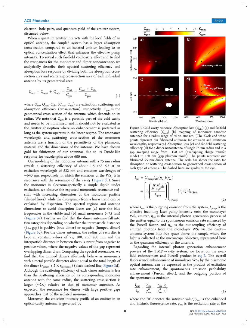
optical antenna, the coupled system has a larger absorptioncross-section compared to an isolated emitter, leading to anoptical concentration effect that enhances the effective pumpintensity. To reveal such far-field cold-cavity effect and to findthe resonances for the monomer and dimer nanoantennae, weanalytically describe their spectral scattering efficiency andabsorption loss response by dividing both the absorption cross-section area and scattering cross-section area of each individualantenna by its geometrical area:
= + = =+
Q Q QCC
C CCext scat abs
ext
geo
scat abs
geo (1)
where Qext, Qscat, Qabs (Cscat, Cabs) are extinction, scattering, andabsorption efficiency (cross-section), respectively. Cgeo is thegeometrical cross-section of the antenna, which depends on itsradius. We note that Qabs is a parasitic part of the cold cavityand needs to be minimized, and it should not be evaluated asthe emitter absorption where an enhancement is preferred aslong as the system operates in the linear regime. The resonancewavelength and scattering cross-section of the monomerantenna are a function of the permittivity of the plasmonicmaterial and the dimensions of the antenna. We have chosengold for fabrication of our antennae due to its Drude-likeresponse for wavelengths above 600 nm.Our modeling of the monomer antenna with a 75 nm radius
reveals a scattering efficiency of about 1.8 and 6.3 at anexcitation wavelength of 532 nm and emission wavelength of∼640 nm, respectively, in which the emission of the WS2 is inresonance with the resonance of the cavity (Figure 3b). Sincethe monomer is electromagnetically a simple dipole underexcitation, we observe the expected monotonic resonance red-shift with increasing dimension of the monomer particle(dashed lines), while the discrepancy from a linear trend can beexplained by dispersion. The spectral regions and antennadimensions to avoid absorption losses are (a) near the bluefrequencies in the visible and (b) small monomers (<75 nm)(Figure 3a). Further we find that the dimer antennae fall intotwo categories depending on whether the interparticle distances(i.e., gap) is positive (true dimer) or negative (lumped dimer)(Figure 3c). For the dimer antennae, the radius of each disc iskept at constant values of 75, 100, and 200 nm and theinterparticle distance in between them is swept from negative topositive values, where the negative values of the gap representoverlapping dimer discs. Comparing the spectral resonances, wefind that the lumped dimers effectively behave as monomerswith a metal particle diameter about equal to the total length ofthe dimer (rdimer ≈ 2 × rmonomer) (black dashed line, Figure 3d).Although the scattering efficiency of each dimer antenna is lessthan the scattering efficiency of its corresponding monomerantenna with the same radius, the scattering cross-section islarger (∼2×) relative to that of monomer antennae. Asexpected, the resonance for dimers with large positive gapsapproaches that of the isolated monomer.Moreover, the emission intensity profile of an emitter in an
optical-cavity antenna is governed by
∬
η η=
= ·
λ
λ
| || |
‐
‐
⎡
⎣
⎢⎢⎢
⎛
⎝⎜⎜⎜
⎞
⎠⎟⎟⎟
⎤
⎦
⎥⎥⎥
I I
Is
CF
( ) ( )( )
d[ QE]
EE
out pump eff int oc
0geo
Pump
p Emit
2
02
(2)
where Iout is the outgoing emission from the system, Ipump is theeffective incoming laser pump intensity onto the monolayerWS2 emitter, ηint is the internal photon generation process ofthe emitter equal to the spontaneous emission rate enhanced bythe Purcell factor, and ηoc is the out-coupling efficiency ofemitted photons from the monolayer WS2 via the cavity−antenna system into free space above the sample where thelight is collected at the microscope objective, represented hereas the quantum efficiency of the antenna.Regarding the internal photon generation enhancement
process of the TMD−cavity system, we focus on the near-field enhancement and Purcell product in eq 2. The overallfluorescence enhancement of monolayer WS2 by the plasmonicoptical antenna can be expressed as the product of excitationrate enhancement, the spontaneous emission probabilityenhancement (Purcell effect), and the outgoing portion ofthe spontaneous emission:
γγ
γγ
γγ
= =IIout
0
em
em0
exc
exc0
r
r0
(3)
where the “0” denotes the intrinsic value, γem is the enhancedand intrinsic fluorescence rate, γexc is the excitation rate at the
Figure 3. Cold cavity response. Absorption loss (Qabs) (a) and far-fieldscattering efficiency (Qscat) (b) mapping of monomer nanodiscantennae for a radius range of 50 to 200 nm. (The black and whitepoints represent our fabricated antennae for emission and excitationwavelengths, respectively.) Absorption loss (c) and far-field scatteringefficiency (d) for a dimer nanoantenna of single 75 nm radius and in agap sweeping range from −150 nm (overlapping charge transfermode) to 150 nm (gap plasmon mode). The points represent ourfabricated 75 nm dimer antenna. The scale bar shows the ratio forabsorption or scattering cross-section to geometrical cross-section ofeach type of antenna. The dashed lines are guides to the eye.
ACS Photonics Article
DOI: 10.1021/acsphotonics.7b00208ACS Photonics XXXX, XXX, XXX−XXX
D
excitation wavelength of 532 nm, and γr is the radiative decayrate of the emitter at an emission wavelength of 640 nm. Sincethe emitter is excited optically, the excitation rate enhancementis then proportional to the ratio of the squared electric field ofthe emitter with the optical cavity and without the cavity (γexc/γexc0 = |E|2/|E0|
2). It is tempting to consider the peak fieldenhancement of a dimer antenna as the anticipated enhance-ment of the emission. This is however not an accurateinterpretation of the actual experiment; because the spot size ofour pump laser is significantly larger than the physical area ofthe antennae, the excitation and hence the photon generationare not local, hot-spot-like effects, but rather originate from anaverage across the pump beam radius. In order to obtain (a) anaccurate emission enhancement originating from a ∼0.8 μmlarge pump diameter and (b) a complete picture of the natureof the electric field enhancement distribution in the presence of
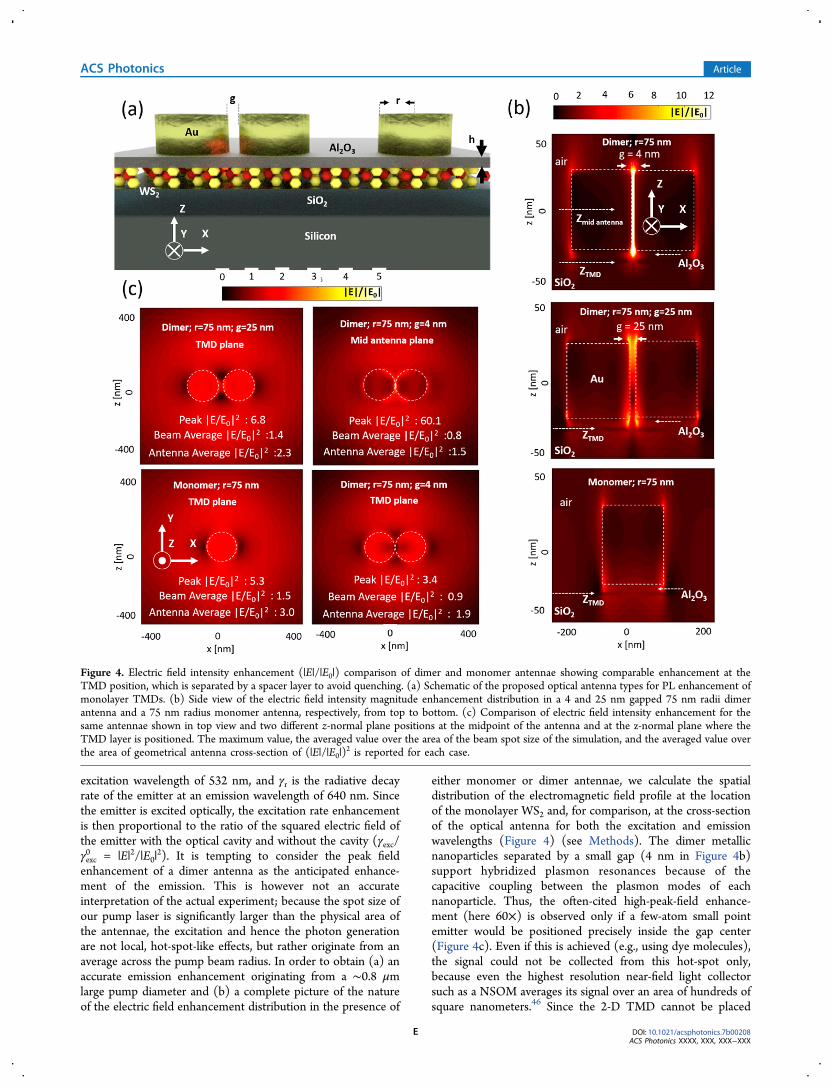
either monomer or dimer antennae, we calculate the spatialdistribution of the electromagnetic field profile at the locationof the monolayer WS2 and, for comparison, at the cross-sectionof the optical antenna for both the excitation and emissionwavelengths (Figure 4) (see Methods). The dimer metallicnanoparticles separated by a small gap (4 nm in Figure 4b)support hybridized plasmon resonances because of thecapacitive coupling between the plasmon modes of eachnanoparticle. Thus, the often-cited high-peak-field enhance-ment (here 60×) is observed only if a few-atom small pointemitter would be positioned precisely inside the gap center(Figure 4c). Even if this is achieved (e.g., using dye molecules),the signal could not be collected from this hot-spot only,because even the highest resolution near-field light collectorsuch as a NSOM averages its signal over an area of hundreds ofsquare nanometers.46 Since the 2-D TMD cannot be placed
Figure 4. Electric field intensity enhancement (|E|/|E0|) comparison of dimer and monomer antennae showing comparable enhancement at theTMD position, which is separated by a spacer layer to avoid quenching. (a) Schematic of the proposed optical antenna types for PL enhancement ofmonolayer TMDs. (b) Side view of the electric field intensity magnitude enhancement distribution in a 4 and 25 nm gapped 75 nm radii dimerantenna and a 75 nm radius monomer antenna, respectively, from top to bottom. (c) Comparison of electric field intensity enhancement for thesame antennae shown in top view and two different z-normal plane positions at the midpoint of the antenna and at the z-normal plane where theTMD layer is positioned. The maximum value, the averaged value over the area of the beam spot size of the simulation, and the averaged value overthe area of geometrical antenna cross-section of (|E|/|E0|)
2 is reported for each case.
ACS Photonics Article
DOI: 10.1021/acsphotonics.7b00208ACS Photonics XXXX, XXX, XXX−XXX
E
inside the gap nor right underneath the metal nanoparticle (toavoid quenching), the only logical position would be to place itbelow or above the antenna, separated by a thin spacer (Figure4a). Thus, when we measure the field enhancement at theposition of a TMD flake residing at an optimized length of 8nm beneath the metal nanoparticle, the peak field enhancementis only 3.4-fold (Figure 4c). We observe a similar trend for the100 and 200 nm radius dimer antennae (SupportingInformation). It is thus not plausible to simply take the peakintensity as the emission process enhancing value. One canconclude that for nonpoint emitters such as the 2-D WS2 flake,it becomes necessary to define an averaged excitation fieldenhancement factor such as by integrating the emission overeither the physical area of the antenna,
∬γγ
=| || |
s
S
dEEexc
exc0
2
02
(4)
or, more accurately, over the pump beam area, where S is eitherthe geometrical cross-section of the antenna or the area of thebeam. The aforementioned peak intensity inside a small (4 nm)gap dimer of 60 drops to 1.5 (0.8) when averaged over theantenna (beam) area at the unphysical midgap dimer position.For the same antenna, the 3.4× enhancement at the TMDplane underneath the cavity drops to 1.9 (0.9) when averagedover the antenna (beam) (Figure 4c). This shows that no actualexcitation rate enhancement is expected for small-gap dimerswhen TMDs are sitting at a quenching-safe distance away fromthe antenna. Interestingly, when the gap is increased from 4 nmto 25 nm (as studied here), the average enhancement for theantenna (beam) increases by 21% (53%) compared to thenarrower hot-spot gap dimer case. We also note that themonomer with the same radius offers the highest antenna andbeam enhancement (Figure 4c, bottom left corner); with thesimpler fabrication of monomers over dimers, these resultssuggest that monomers are equally well-performing to enhance2D material PL.A comparison of the far-field (scattering efficiency of disc
antenna) and near-field spectra (electric field enhancement) ofindividual Au nanodiscs (Supporting Information) shows thatthe far-field scattering efficiency peaks at a larger nanoparticlesize than the near-field intensity enhancement. Consequently,one should acknowledge that maximum scattering efficiency isnot synonymous with highest near-field enhancement, asclaimed also in previous studies.47−49 Also, often in optics weseek the highest possible quality factor (Q factor) for thehighest possible light−matter interaction; but in a high-performing antenna we seek the opposite because we desireradiation losses.26,49
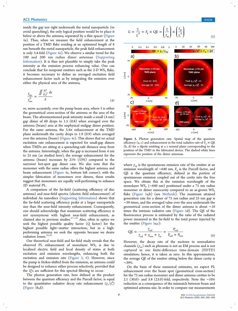
Our theoretical near-field and far-field study reveals that theobserved PL enhancement of monolayer WS2 is due tolocalized electric field and local density of states at bothexcitation and emission wavelengths, enhancing both theexcitation and emission rate (Figure 3, 4). However, sincethe pump is Stokes-shifted from the emission, an antenna couldbe designed to enhance either process selectively, provided thatthe Q’s are sufficient for this spectral filtering to occur.The photon generation rate, here defined as the product
between the quantum efficiency and the Purcell factor, is equalto the quantitative radiative decay rate enhancement (γr/γr
0)(Figure 5b,d):
γγ
γγ
γ
γ= = × = ×
⎛⎝⎜⎜
⎞⎠⎟⎟
⎛⎝⎜⎜
⎞⎠⎟⎟G F QEr
r0 p
r
sp
sp
r0
(5)
where γsp is the spontaneous emission rate of the emitter at anemission wavelength of ∼640 nm, Fp is the Purcell factor, andQE is the quantum efficiency, defined as the portion ofspontaneous emission coupled out of the cavity into the freespace. We obtain this at the emission wavelength of themonolayer WS2 (∼640 nm) positioned under a 75 nm radiusmonomer or dimer nanocavity compared to an as-grown WS2flake (Figure 5a,b) (see Methods). The maximum attainedgeneration rate for a dimer of 75 nm radius and 25 nm gap is∼39 times, and the averaged value over the area underneath thegeometrical cross-section of the dimer antenna is about ∼10times the intrinsic radiative rate (Figure 5d). The QE of thefluorescence process is estimated by the ratio of the radiatedpower measured in the far-field to the total power injected bythe emitter (Figure 5a,c):
γγ γ γ
=+ +
=+P
P PQE rad
rad loss nr
rad
rad loss (6)
However, the decay rate of the excitons to nonradiativechannels (γnr) such as phonons is not an EM process and is notcaptured in our finite-difference time-domain (FDTD)simulation; hence, it is taken as zero. In this approximation,the average QE of the emitter sitting below the dimer cavity is∼39%.On the basis of these numerical estimates, we expect PL
enhancement over the beam spot (geometrical cross-section)for the 75 nm radius monomer and dimer antenna cavities to be2.1 (30.0)- and 3.8 (23.0)-fold, respectively. Note the ∼10×reduction as a consequence of the mismatch between beam andoptimized antenna size. In order to compare our measurements
Figure 5. Photon generation rate. Spatial map of the quantumefficiency (a, c) and enhancement in the total radiative rate of Fp × QE(b, d) for a dipole emitting at a z normal plane corresponding to theposition of the TMD in the fabricated device. The dashed white linesrepresent the position of the dimer antennae.
ACS Photonics Article
DOI: 10.1021/acsphotonics.7b00208ACS Photonics XXXX, XXX, XXX−XXX
F
to the modeling, we fit the experimental beam intensity profileto a Gaussian function and take the full width at half-maximum(fwhm) as the beam spot size (Figure 2c). These experimentalresults corroborate our computational expectations, but showslightly lower values. Another common way of expressingexperimental results is to define the normalized experimentalenhancement factor (⟨EFexp⟩) as
27
=II
SS
EF /expcav
0
cav
0 (7)
where Scav is the area of a cavity, S0 is the area of the Gaussianexcitation beam, Icav is the PL intensity from the cavity, and I0 isthe PL intensity from the as-grown WS2 flake, resulting in an⟨EFexp⟩ of 50.9- and 39.7-fold. This evaluation leads to anoverestimation of the local enhancement within the cavity fromour experimental result, because per our simulation the electricfield intensity and Purcell factor distribution directly under thenanoantenna are significantly larger than the area around theantenna Scav. Consequently, our findings point to the need foran evaluation of the field enhancement over a much larger areathan Scav in order to deduce realistic material properties fromthe cavity experiments.The shape of the PL spectrum in the cavity is conceptually
similar to that of the control sample. However, we observe aspectral narrowing in fwhm value from 16.7 nm to 15.7, 13.5,and 14.6 nm for the cases of the 75 nm radius monomer discantenna and the 75 and 100 nm radii dimer antennae,respectively. We note that these effects are not sustained for thePL spectrum of the 200 nm radius dimer antenna, for which weobserve a red-shift by 3.5 nm (relative to the intrinsic emissionspectrum of as-grown WS2 flakes) and a band broadening to21.8 nm. We attribute this observation to convolution of the PLemission spectrum of monolayer WS2 with the fundamentalresonance of the 200 nm dimer cavity (SupportingInformation). Supporting modeling indicates narrowing of theemission spectrum with the dot radius, so that for the cases ofthe 75 and 100 nm radii dimers the resonance condition affectsnarrowing and not broadening of the WS2 emission peak. Thisresults in a higher quality factor and sharper spectral response(Supporting Information), in line with a prediction based onWheeler’s limit.50 Our experimental findings highlight that thequality factor of nanoantennae increases as the dimensions ofthe disc decrease.In conclusion, we have demonstrated that optical nano-
antennae can be used to control the emitting properties ofmonolayer TMDs. This control was achieved using two typesof metallic cavities (monomer vs dimer) at four different sizes.These emission dynamics were also supported by numericalcalculations. In particular, we have demonstrated thefluorescent enhancement of 2-D materials, and unlike quantumdots there is an areal average effect that has to be taken intoaccount. We have also observed band narrowing of theemission response when the resonance of the cavitycorresponds to the emission wavelength of monolayer WS2.Both monomer and dimer nanoantenna architectures arescalable to emission resonances of other members of theTMD family as well including MoTe2, which emits at atelecommunication wavelength in the near-infrared. Thedemonstrated nanoantenna-controlled emission from a mono-layer WS2 flake could open a pathway to visible light sourcesbased on lithographically fabricated nanoantennae supporting avariety of optoelectronic applications.51−56
■ METHODS
Growth Method. Single- and multilayer tungsten disulfide(WS2) was grown via ambient-pressure chemical vapordeposition utilizing a tube furnace. The process is a variationof our previously published work on transition metaldichalcogenide materials.57−59 The reagents were ammoniameta tungstate (AMT) and elemental sulfur. The process startsby spin-coating a 3.1 mmol aqueous solution of AMT onto aSiO2/Si substrate. The resultant residue serves as the tungstensource for our CVD growth. We place a target substrate directlyface-down onto this source substrate and insert this stack intothe growth region at the center of the process tube in our tubefurnace. An alumina boat containing elemental sulfur is placedinside the process tube far enough upstream of the furnaceheating coil so that it just fully melts when the furnace centerreaches the peak growth temperature of 850 °C.The temperature ramp for WS2 growth commences after a
nitrogen purge of the process tube for 15 min at 5 scfh. Afterthat we ramp the furnace to 500 °C to decompose the AMTinto tungsten trioxide, releasing water and ammonia vapor.After 20 min the reaction is complete, and we ramp up to thegrowth temperature of 850 °C and remain there for 15 min.Subsequently, the furnace is allowed to cool naturally to 200 °Cbefore the process tube is opened to air and the target substrateretrieved.
Fabrication Method. After WS2 films were deposited, a ∼8nm layer of aluminum oxide (Al2O3) was deposited onto thesample as a spacer between the emitter and the plasmonicantennae. Next, we fabricated monomer and dimer optical diskantennae, varying the diameters and gaps, onto the large-areaWS2 film using electron beam lithography. We then followedwith gold deposition using electron beam evaporation. Finallythe gold film is lifted off using a PG remover. Lithographicalfabrication of the antennae allows for control over dimensionsand position of particles, permitting us to tune the plasmonicresonance of each antenna element. The nanoantenna werearranged at a center-to-center distance of 4 μm to preventinterference of absorption cross-sections of individual antennae(Supporting Information).
Raman and Photoluminescence Spectroscopy. Ramanand PL spectroscopy were performed using a custom-builtspectrometer equipped with a 532 nm excitation laser and aCCD detector (Supporting Information). The nonlinearemission spectra were acquired in reflection geometry to aspectrometer including a 532 nm notch filter to reject the pumpwavelengths. The spectrometer acquisition parameters wereheld constant and set to ensure high signal-to-noise ratio for theweakest signal. All measurements were performed in air at ∼25°C and atmospheric pressure.
Reflectance Spectroscopy. Reflectance measurementswere performed using a 20 W halogen light source bymeasuring the difference in reflected intensity from the WS2/SiO2 and bare silicon wafer substrate and normalizing this tothe substrate-reflected intensity. For optical microscopy, weused white light and a 100× objective lens.
FDTD Calculation Method. Reflectance, in-plane and out-of-plane electric field intensities, Purcell factor, scattering, andabsorption spectra were calculated. Optical constants of WS2were obtained from Liu et al.60 The refractive indexes of silica,silicon, alumina, and gold were used directly from Palik as wellas Johnson and Christy.61,62
ACS Photonics Article
DOI: 10.1021/acsphotonics.7b00208ACS Photonics XXXX, XXX, XXX−XXX
G
We used the Lumerical three-dimensional FDTD solver forall Maxwell equation calculations. For scattering effectcalculations, we employed a total field scattered field (TFSF)method. The plane wave was launched normally from the topof monomer or dimer antennae. Two (virtual) power-flowmonitors (six detectors each) were positioned inside andoutside the TFSF source, surrounding the antenna, to measurethe absorption and scattering cross sections, in order. Thepower flow analysis calculates the net absorbed power andscattered power from the particle. For Purcell factorcalculations, a dipole source was used (Supporting Informa-tion). In all other problems, a normal incident broadband planewave was implemented. To ensure that scattered light does notreturn to the simulation region, a perfect matching layer wasapplied as boundary condition in all directions.For Purcell factor and quantum efficiency calculations, we
sampled the plane at the level of the 2-D TMD sheet with adipole source. We calculated the radiated power by a set of(virtual) field power monitors as one transmission boxsurrounding only the dipole source and another transmissionbox far away from the source but surrounding both the emitterand cavity. The expression deployed in this method to evaluatethe Purcell factor is Fp = emitted-power ( f)/source-power ( f),where f is the optical frequency. The source-power returns thepower that the dipole would radiate in a homogeneous material.The emitted-power is the power transmitted out of a boxedarea surrounding the dipole source due to the dispersivematerials used in the cavity.
■ ASSOCIATED CONTENT
*S Supporting InformationThe Supporting Information is available free of charge on theACS Publications website at DOI: 10.1021/acsphoto-nics.7b00208.
Description of near-field intensity distribution, scatteringefficiency, absorption loss map, and quality factor for alldimer antennae; additional Purcell factor results for anarrow gap dimer antenna; nanoantenna fabricationsteps and SEM images; PL measurement setup; DFTcalculation results (PDF)
■ AUTHOR INFORMATION
Corresponding Author*E-mail: [email protected].
ORCID
Mohammad H. Tahersima: 0000-0001-6759-8869M. Danang Birowosuto: 0000-0002-9997-6841Volker J. Sorger: 0000-0002-5152-4766NotesThe authors declare no competing financial interest.
■ ACKNOWLEDGMENTS
We thank the National Science Foundation and the MaterialsGenome Initiative for support under the award number NSFDMREF 14363300/1455050 and NSF EAPSI 1613966. V.S. issupported by the Air Force Office of Scientific Research YoungInvestigator Program under grants FA9550-14-1-0215 andFA9550-14-1-0378.
■ REFERENCES(1) Mak, K. F.; Lee, C.; Hone, J.; Shan, J.; Heinz, T. F. AtomicallyThin MoS2: A New Direct-Gap Semiconductor. Phys. Rev. Lett. 2010,105, 136805.(2) Splendiani, A.; Sun, L.; Zhang, Y.; Li, T.; Kim, J.; Chim, C. Y.;Galli, G.; Wang, F. Emerging Photoluminescence in Monolayer MoS2.Nano Lett. 2010, 10, 1271−1275.(3) Gutierrez, H. R.; Perea-Lopez, N.; Elías, A. L.; Berkdemir, A.;Wang, B.; Lv, R.; Lopez-Urías, F.; Crespi, V. H.; Terrones, H.;Terrones, M. Extraordinary Room-Temperature Photoluminescence inTriangular WS2Monolayers. Nano Lett. 2013, 13, 3447−3454.(4) Peimyoo, N.; Shang, J.; Cong, C.; Shen, X.; Wu, X.; Yeow, E. K.L.; Yu, T. Nonblinking, Intense Two-Dimensional Light Emitter:Monolayer WS2 Triangles. ACS Nano 2013, 7, 10985−10994.(5) Xia, F.; Wang, H.; Xiao, D.; Dubey, M.; Ramasubramaniam, A.Two-dimensional material nanophotonics. Nat. Photonics 2014, 8,899−907.(6) Tahersima, M. H.; Sorger, V. J. Enhanced photon absorption inspiral nanostructured solar cells using layered 2D materials. Nano-technology 2015, 26, 344005.(7) Ma, Z.; Tahersima, M. H.; Khan, S.; Sorger, V. J. Two-Dimensional Material-Based Mode Confinement Engineering inElectro-Optic Modulators. IEEE J. Sel. Top. Quantum Electron. 2017,23, 81−88.(8) Britnell, L.; et al. Strong light−matter interactions inheterostructures of atomically thin films. Science 2013, 340, 1311−1314.(9) Lopez-Sanchez, O.; Lembke, D.; Kayci, M.; Radenovic, A.; Kis, A.Ultrasensitive photodetectors based on monolayer MoS2. Nat.Nanotechnol. 2013, 8, 497−501.(10) Cheng, R.; et al. Electroluminescence and photocurrentgeneration from atomically sharp WSe2/MoS2 heterojunction p−ndiodes. Nano Lett. 2014, 14, 5590−5597.(11) Yang, W.; et al. Electrically Tunable Valley-Light EmittingDiode (vLED) Based on CVD-Grown Monolayer WS2. Nano Lett.2016, 16, 1560−1567.(12) Mak, K. F.; He, K.; Lee, C.; Lee, G. H.; Hone, J.; Heinz, T. F.;Shan, J. Tightly bound trions in monolayer MoS2. Nat. Mater. 2013,12, 207−211.(13) Wang, Z.; Zhao, L.; Mak, K. F.; Shan, J. Probing the Spin-Polarized Electronic Band Structure in Monolayer Transition MetalDichalcogenides by Optical Spectroscopy. Nano Lett. 2017, 17, 740−746.(14) Shang, J.; Shen, X.; Cong, C.; Peimyoo, N.; Cao, B.; Eginligil,M.; Yu, T. Observation of Excitonic Fine Structure in a 2D Transition-Metal Dichalcogenide Semiconductor. ACS Nano 2015, 9, 647−655.(15) Wang, X. H.; Ning, J. Q.; Su, Z. C.; Zheng, C. C.; Zhu, B. R.;Xie, L.; Wu, H. S.; Xu, S. J. Photoinduced doping and photo-luminescence signature in an exfoliated WS2 monolayer semi-conductor. RSC Adv. 2016, 6, 27677−27681.(16) Chernikov, L.; Berkelbach, T. C.; Hill, H. M.; Rigosi, A.; Li, Y.;Aslan, O. B.; Reichman, D. R.; Hybertsen, M. S.; Heinz, T. F. ExcitonBinding Energy and Nonhydrogenic Rydberg Series in MonolayerWS2. Phys. Rev. Lett. 2014, 113, 076802.(17) Plechinger, G.; Nagler, P.; Kraus, J.; Paradiso, N.; Strunk, C.;Schuller, C.; Korn, T. Identification of excitons, trions and biexcitonsin single-layer WS2. Phys. Status Solidi RRL 2015, 9, 457−461.(18) You, Y.; Zhang, X.; Berkelbach, T. C.; Hybertsen, M. S.;Reichman, D. R.; Heinz, T. F. Observation of biexcitons in monolayerWSe2. Nat. Phys. 2015, 11, 477−481.(19) Ye, Z.; Cao, T.; O’Brien, K.; Zhu, H.; Yin, X.; Wang, Y.; Louie,S. G.; Zhang, X. Probing excitonic dark states in single-layer tungstendisulphide. Nature 2014, 513, 214−218.(20) Gan, X.; Gao, Y.; Mak, K. F.; Yao, X.; Shiue, R. J.; Zande, A.;Trusheim, M.; Hatami, F.; Heinz, T. F.; Hone, J.; Englund, D.Controlling the spontaneous emission rate of monolayer MoS2 in aphotonic crystal nanocavity. Appl. Phys. Lett. 2013, 103, 181119.(21) Ye, Y.; Wong, Z. J.; Lu, X.; Ni, X.; Zhu, H.; Chen, X.; Wang, Y.;Zhang, X. Monolayer excitonic laser. Nat. Photonics 2015, 9, 733−737.
ACS Photonics Article
DOI: 10.1021/acsphotonics.7b00208ACS Photonics XXXX, XXX, XXX−XXX
H
(22) Taghinejad, H.; Taghinejad, M.; Tarasov, A.; Tsai, M. Y.;Hosseinnia, A. H.; Moradinejad, H.; Campbell, P. M.; Eftekhar, A. A.;Vogel, E. M.; Adibi, A. Resonant Light-Induced Heating in HybridCavity-Coupled 2D Transition-Metal Dichalcogenides. ACS Photonics2016, 3, 700−707.(23) Mukherjee, B.; Kaushik, N.; Tripathi, R. P. N.; Joseph, A. M.;Mohapatra, P. K.; Dhar, S.; Singh, B. P.; Kumar, G. V. P.; Simsek, E.;Lodha, S. Exciton Emission Intensity Modulation of Monolayer MoS2via Au Plasmon Coupling. Sci. Rep. 2017, 7, No. 41175.(24) Taghinejad, H.; Shams-Mousavi, S. H.; Gong, Y.; Taghinejad,M.; Eftekhar, A. A.; Ajayan, P.; Adibi, A. Lattice Plasmon InducedLarge Enhancement of Excitonic Emission in Monolayer MetalDichalcogenides. Plasmonics 201610.1007/s11468-016-0470-4.(25) Purcell, E. M.; Torrey, H. C.; Pound, R. V. Phys. Rev. 1946, 69,37.(26) Eggleston, M. S.; Messer, K.; Zhang, L.; Yablonovitch, E.; Wu,M. C. Optical antenna enhanced spontaneous emission. Proc. Natl.Acad. Sci. U. S. A. 2015, 112, 1704−1709.(27) Akselrod, G. M.; Ming, T.; Argyropoulos, C.; Hoang, T. B.; Lin,Y.; Ling, X.; Smith, D. R.; Kong, J.; Mikkelsen, M. H. LeveragingNanocavity Harmonics for Control of Optical Processes in 2DSemiconductors. Nano Lett. 2015, 15, 3578−3584.(28) Butun, S.; Tongay, S.; Aydin, K. Enhanced Light Emission fromLarge-Area Monolayer MoS2 Using Plasmonic Nanodisc Arrays. NanoLett. 2015, 15, 2700−2704.(29) Kern, J.; Trugler, A.; Niehues, I.; Ewering, J.; Schmidt, R.;Schneider, R.; Najmaei, S.; George, A.; Zhang, J.; Lou, J.; Hohenester,U.; Vasconcellos, S. M.; Bratschitsch, R. Nanoantenna-EnhancedLight−Matter Interaction in Atomically Thin WS2. ACS Photonics2015, 2, 1260−1265.(30) Lee, B.; Park, J.; Han, G. H.; Ee, H. S.; Naylor, C. H.; Liu, W.;Johnson, A. T. C.; Agarwal, R. Fano Resonance and SpectrallyModified Photoluminescence Enhancement in Monolayer MoS2Integrated with Plasmonic Nanoantenna Array. Nano Lett. 2015, 15,3646−3653.(31) Liu, W.; Lee, B.; Naylor, C. H.; Ee, H. S.; Park, J.; Johnson, A. T.C.; Agarwal, R. Strong exciton-plasmon coupling in MoS2 coupledwith plasmonic lattice. Nano Lett. 2016, 16, 1262−1269.(32) Eggleston, M.; Desai, S.; Messer, K.; Madhvapathy, S.; Xiao, J.;Zhang, X.; Yablonovitch, E.; Javey, A.; Wu, M. C. EnhancedSpontaneous Emission from an Optical Antenna Coupled WSe_2Monolayer. Technol. Dig. Ser. - Opt. Soc. Am. 2015, DOI: 10.1364/CLEO_QELS.2015.FTu1E.5.(33) Najmaei, S.; Mlayah, A.; Arbouet, A.; Girard, C.; Leotin, J.; Lou,J. Plasmonic Pumping of Excitonic Photoluminescence in HybridMoS2-Au Nanostructures. ACS Nano 2014, 8, 12682−12689.(34) Bhanu, U.; Islam, M. R.; Tetard, L.; Khondaker, S. I.Photoluminescence Quenching in Gold MoS2 Hybrid Nanoflakes.Sci. Rep. 2015, 4, 5575.(35) Zhu, Z.; et al. Excitonic Resonant Emission−Absorption ofSurface Plasmons in Transition Metal Dichalcogenides for Chip-LevelElectronic−Photonic Integrated Circuits. ACS Photonics 2016, 3, 869−874.(36) Anger, P.; Bharadwaj, P.; Novotny, L. Enhancement andquenching of single-molecule fluorescence. Phys. Rev. Lett. 2016, 96,3−6.(37) Cho, C. H.; Aspetti, C. O.; Turk, M. E.; Kikkawa, J. M.; Nam, S.W.; Agarwal, R. Tailoring hot-exciton emission and lifetimes insemiconducting nanowires via whispering-gallery nanocavity plasmons.Nat. Mater. 2011, 10, 669−675.(38) Sorger, V. J.; Pholchai, N.; Cubukcu, E.; Oulton, R. F.; Kolchin,P.; Borschel, C.; Gnauck, M.; Ronning, C.; Zhang, X. StronglyEnhanced Molecular Fluorescence inside a Nanoscale Waveguide Gap.Nano Lett. 2011, 11, 4907−4911.(39) Chen, H.; Yang, J.; Rusak, E.; Straubel, J.; Guo, R.; Myint, Y. W.;Pei, J.; Decker, M.; Rockstuhl, C.; Lu, Y.; Kivshar, Y. S.; Neshev, D.Manipulation of photoluminescence of two-dimensional MoSe2 bygold nanoantennas. Sci. Rep. 2016, 6, 22296.
(40) Sobhani, A.; Lauchner, A.; Najmaei, S.; Ayala-Orozco, C.; Wen,F.; Lou, J.; Halas, N. J. Enhancing the photocurrent and photo-luminescence of single crystal monolayer MoS2 with resonantplasmonic nanoshells. Appl. Phys. Lett. 2014, 104, 031112.(41) Cui, Y.; et al. High-Performance Monolayer WS2 Field-EffectTransistors on High-κ Dielectrics. Adv. Mater. 2015, 27, 5230−5234.(42) Wang, X. H.; Ning, J. Q.; Zheng, C. C.; Zhu, B. R.; Xie, L.; Wu,H. S.; Xu, S. J. Photoluminescence and Raman mapping character-ization of WS2 monolayers prepared using top-down and bottom-upmethods. J. Mater. Chem. C 2015, 3, 2589−2592.(43) Berkdemir, A.; et al. Identification of individual and few layers ofWS2 using Raman Spectroscopy. Sci. Rep. 2013, 3, 1755.(44) Zhao, W.; Ghorannevis, Z.; Chu, L.; Toh, M.; Kloc, C.; Tan, P.-H.; Eda, G. Evolution of Electronic Structure in Atomically ThinSheets of WS2 and WSe2. ACS Nano 2013, 7, 791−797.(45) Lee, Y.-H.; Zhang, X.-Q.; Zhang, W.; Chang, M.-T.; Lin, C.-T.;Chang, K.-D.; Yu, Y.-C.; Wang, J. T.-W.; Chang, C.-S.; Li, L.-J.; Lin, T.-W. Synthesis of Large-Area MoS 2 Atomic Layers with ChemicalVapor Deposition. Adv. Mater. 2012, 24, 2320−2325.(46) Oshikane, Y.; Kataoka, T.; Okuda, M.; Hara, S.; Inoue, H.;Nakano, M. Observation of nanostructure by scanning near-fieldoptical microscope with small sphere probe. Sci. Technol. Adv. Mater.2007, 8, 18110.1016/j.stam.2007.02.013(47) Yan, B.; Boriskina, S. V.; Reinhard, B. M. Design andImplementation of Noble Metal Nanoparticle Cluster Arrays forPlasmon Enhanced Biosensing. J. Phys. Chem. C 2011, 115 (50),24437−24453.(48) Biagioni, P.; Huang, J. S.; Hecht, B. Nanoantennas for Visibleand Infrared Radiation. Rep. Prog. Phys. 2012, 75, 024402.(49) Bonakdar, A.; Mohseni, H. Impact of optical antennas on activeoptoelectronic devices. Nanoscale 2014, 6, 10961.(50) Wheeler, H. Small antennas. IRE Trans. Antennas Propag. 1975,AP-24, 462−469.(51) Li, N.; Liu, K.; Sadana, D. K.; Sorger, V. J. Nano III-V PlasmonicLight-Sources for Monolithic Integration on Silicon. Sci. Rep. 2015, 5,14067.(52) Liu, K.; Li, N.; Sadana, D. K.; Sorger, V. J. Integrated nano-cavity plasmon light-sources for on-chip optical interconnects. ACSPhotonics 2016, 3, 233−242.(53) Fratalocchi, A.; Dodson, C. M.; Zia, R.; Genevet, P.; Verhagen,E.; Altug, H.; Sorger, V. J Nano-optics gets practical: PlasmonModulators. Nat. Nanotechnol. 2015, 10, 11−15.(54) Birowosuto, M. D.; Takiguchi, M.; Olivier, A.; Tobing, L. Y.;Kuramochi, E.; Yokoo, A.; Hong, W.; Notomi, M. Opt. Commun. 2017,383, 555−560.(55) Ye, C.; Liu, K.; Soref, R.; Sorger, V. J. 3-Waveguide 2 × 2Plasmonic Electro-optic Switch. Nanophotonics 2015, 4 (1), 261−268.(56) Sun, S.; Badaway, A.; Narayana, V.; El-Ghazawi, T.; Sorger, V. J.Photonic-Plasmonic Hybrid Interconnects: Efficient Links with Lowlatency, Energy and Footprint. IEEE Photonics J. 2015, 7, 6.(57) Mann, J.; Sun, D.; Ma, Q.; Preciado, E.; Yamaguchi, K.; Chen, J.-R.; Heinz, T. F.; Kawakami, R.; Bartels, L. Facile Growth of Sub-Millimeter Scale Monolayer MoS2 Films on SiO2/Si. Eur. Phys. J. B2013, 86, 226.(58) Tanabe, I.; et al. Band structure characterization of WS2 grownby chemical vapor deposition. Appl. Phys. Lett. 2016, 108, 252103.(59) Mann, J.; et al. 2-Dimensional Transition Metal Dichalcogenideswith Tunable Direct Band Gaps: MoS2(1-x)Se2x Monolayers. Adv.Mater. 2014, 26, 1399−1404.(60) Liu, H. L.; Shen, C. C.; Su, S. H.; Hsu, C.-L.; Li, M. Y.; Li, L. J.Optical properties of monolayer transition metal dichalcogenidesprobed by spectroscopic ellipsometry. Appl. Phys. Lett. 2014, 105,201905.(61) Palik, E. D. Handbook of Optical Constants of Solids; AcademicPress: Waltham, MA, 1998; Vol. 3.(62) Johnson, P. B.; Christy, R. W. Optical Constants of the NobleMetals. Phys. Rev. B 1972, 6, 4370.
ACS Photonics Article
DOI: 10.1021/acsphotonics.7b00208ACS Photonics XXXX, XXX, XXX−XXX
I