Embed Size (px)
Citation preview
Test Report No.: NK-15-R-056
FCC Certification
Samsung Electronics Co., Ltd. FCC ID : A3LCYLHDE01A
Page 2 of 59
TABLE OF CONTENTS
1. Scope 4
2. Introduction (Site Description) 5
2.1 Test facility 5
2.2 Accreditation and listing 6
3. Test Conditions & EUT Information 7
3.1 Operation During Test 7
3.1.1 Table of test power setting 7
3.1.2 Table of test channels 7
3.1.3 Table of test modes 8
3.1.4 Antenna information 8
3.2 Support Equipment 9
3.3 Setup Drawing 9
3.4 EUT Information 10
4. Summary of Test Results 11
5. Recommendation / Conclusion 12
6. Antenna Requirements 12
7. Description of Test 13
7.1 Conducted Emissions 13
7.2 Radiated Emissions 14
7.3 6 dB Bandwidth 15
7.4 Peak Output Power 16
7.5 Peak Power Spectral Density 17
7.6 Conducted Spurious Emissions 18
7.7 Duty Cycle 19
8. Test Data 20
8.1 Conducted Emissions 20
Test Report No.: NK-15-R-056
FCC Certification
Samsung Electronics Co., Ltd. FCC ID : A3LCYLHDE01A
Page 3 of 59
8.2 Radiated Emissions 23
8.3 6 dB Modulated Bandwidth 25
8.4 Peak Output Power 28
8.5 Peak Power Spectral Density 31
8.6 Conducted Spurious Emissions 34
8.7 Radiated Spurious Emissions 38
8.8 Radiated Band Edge 41
9. Test Equipment 42
10. Accuracy of Measurement 43
Appendix A: Labelling Requirement 45
Appendix B: Photographs of Test Set-up 46
Appendix C: EUT Photographs 49
Appendix D: Maximum Permissible Exposure 58
Test Report No.: NK-15-R-056
FCC Certification
Samsung Electronics Co., Ltd. FCC ID : A3LCYLHDE01A
Page 4 of 59
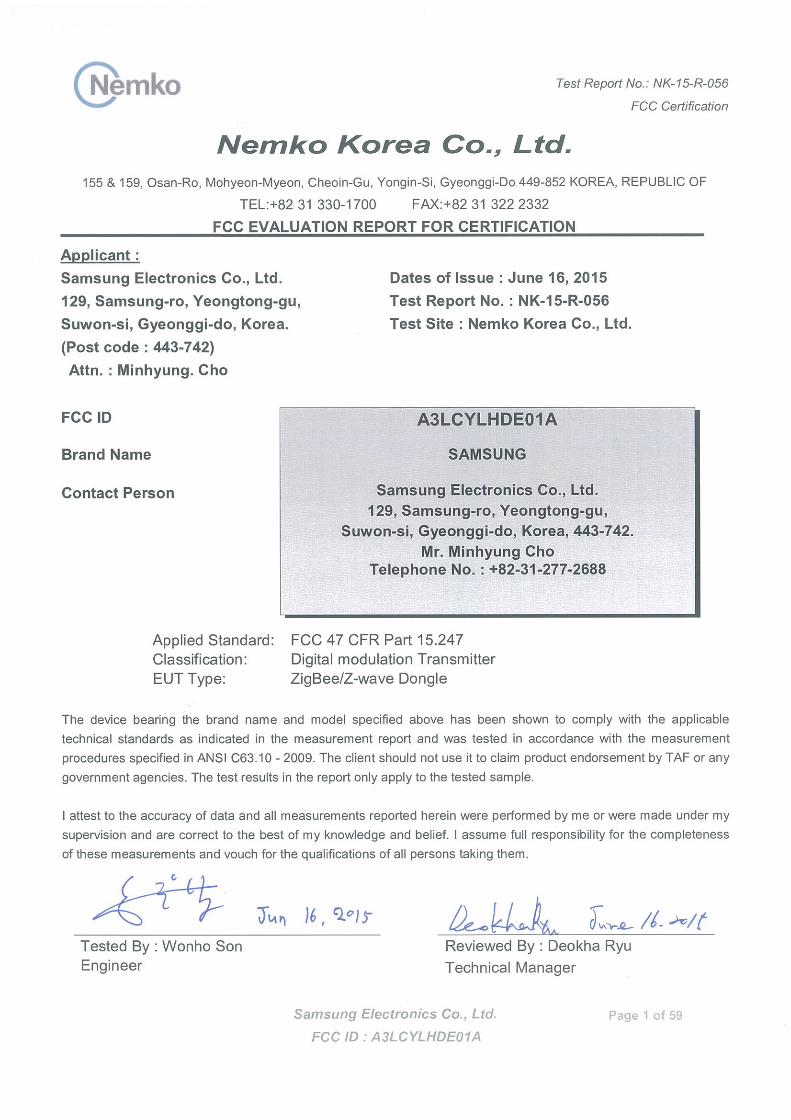
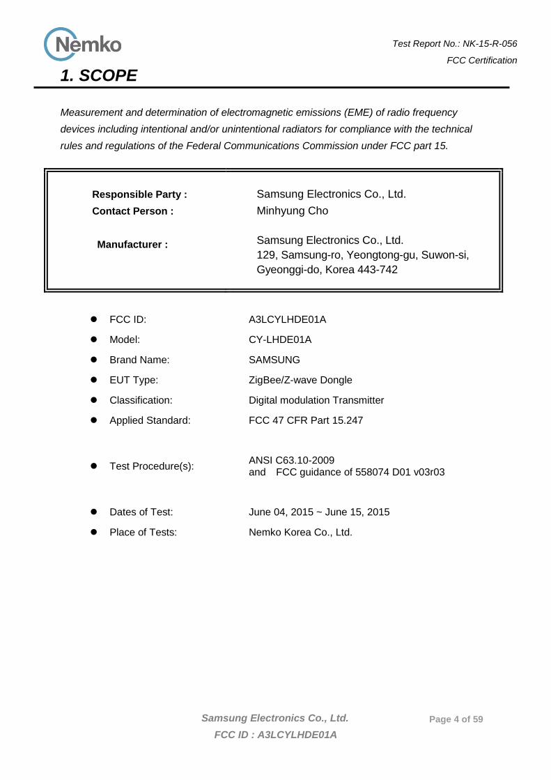
1. SCOPE Measurement and determination of electromagnetic emissions (EME) of radio frequency devices including intentional and/or unintentional radiators for compliance with the technical rules and regulations of the Federal Communications Commission under FCC part 15.
Responsible Party : Contact Person :
Manufacturer :
Samsung Electronics Co., Ltd. Minhyung Cho Samsung Electronics Co., Ltd. 129, Samsung-ro, Yeongtong-gu, Suwon-si, Gyeonggi-do, Korea 443-742
FCC ID: A3LCYLHDE01A
Model: CY-LHDE01A
Brand Name: SAMSUNG
EUT Type: ZigBee/Z-wave Dongle
Classification: Digital modulation Transmitter
Applied Standard: FCC 47 CFR Part 15.247
Test Procedure(s): ANSI C63.10-2009 and FCC guidance of 558074 D01 v03r03
Dates of Test: June 04, 2015 ~ June 15, 2015
Place of Tests: Nemko Korea Co., Ltd.
Test Report No.: NK-15-R-056
FCC Certification
Samsung Electronics Co., Ltd. FCC ID : A3LCYLHDE01A
Page 5 of 59
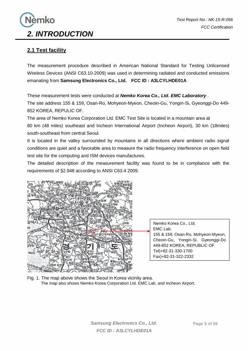
2. INTRODUCTION 2.1 Test facility The measurement procedure described in American National Standard for Testing Unlicensed Wireless Devices (ANSI C63.10-2009) was used in determining radiated and conducted emissions emanating from Samsung Electronics Co., Ltd. FCC ID : A3LCYLHDE01A These measurement tests were conducted at Nemko Korea Co., Ltd. EMC Laboratory . The site address 155 & 159, Osan-Ro, Mohyeon-Myeon, Cheoin-Gu, Yongin-Si, Gyeonggi-Do 449-852 KOREA, REPULIC OF. The area of Nemko Korea Corporation Ltd. EMC Test Site is located in a mountain area at 80 km (48 miles) southeast and Incheon International Airport (Incheon Airport), 30 km (18miles) south-southeast from central Seoul. It is located in the valley surrounded by mountains in all directions where ambient radio signal conditions are quiet and a favorable area to measure the radio frequency interference on open field test site for the computing and ISM devices manufactures. The detailed description of the measurement facility was found to be in compliance with the requirements of §2.948 according to ANSI C63.4 2009.
Fig. 1. The map above shows the Seoul in Korea vicinity area. The map also shows Nemko Korea Corporation Ltd. EMC Lab. and Incheon Airport.
Nemko Korea Co., Ltd. EMC Lab. 155 & 159, Osan-Ro, Mohyeon-Myeon, Cheoin-Gu, Yongin-Si, Gyeonggi-Do 449-852 KOREA, REPUBLIC OF Tel)+82-31-330-1700 Fax)+82-31-322-2332
Test Report No.: NK-15-R-056
FCC Certification
Samsung Electronics Co., Ltd. FCC ID : A3LCYLHDE01A
Page 6 of 59
2.2 Accreditation and listing
Accreditation type Accreditation number
CAB Accreditation for DOC Designation No. KR0026
KOLAS Accredited Lab. (Korea Laboratory Accreditation Scheme) Registration No. 155
Canada IC Registered site Site No. 2040E
VCCI registration site(RE/CE/Telecom CE) Member No. 2118
EMC CBTL -
KCC(RRL)Designated Lab. Registration No. KR0026
Test Report No.: NK-15-R-056
FCC Certification
Samsung Electronics Co., Ltd. FCC ID : A3LCYLHDE01A
Page 7 of 59
3. TEST CONDITIONS & EUT INFORMATION
3.1 Operation During Test The EUT is the transceiver which is the module supporting the Zigbee mode. (1Tx / 1Rx) During the test, the EUT was connected to laptop PC and then a test program was executed to operate duty cycle of EUT continuously (Duty cycle > 98%). The EUT was tested at the lowest channel, middle channel and the highest channel with the maximum output power in accordance with the manufacturer’s specifications. The worst data were recorded in the report. 3.1.1 Table of test power setting
Frequency Power setting Level
2405 MHz 8
2440 MHz 8
2480 MHz -6 3.1.2 Table of test channels
Frequency band Mode Test Channel (CH) Frequency (MHz)
2.4 GHz 802.15.4
11 2405
18 2440
26 2480
Test Report No.: NK-15-R-056
FCC Certification
Samsung Electronics Co., Ltd. FCC ID : A3LCYLHDE01A
Page 8 of 59
3.1.3 Table of test modes
Test Items Mode Data rate (kbps) Test Channel (CH)
Conducted Emissions 802.15.4 250 18
Radiated Emissions 802.15.4 250 18
6 dB Bandwidth 802.15.4 250 11/18/26
Peak Output Power 802.15.4 250 11/18/26
Peak Power Spectral Density 802.15.4 250 11/18/26
Conducted Spurious Emission, Radiated Spurious Emission 802.15.4 250 11/18/26
Band edge Emission 802.15.4 250 11/26
3.1.4 Antenna information:
Frequency band Mode Antenna TX mode Support MIMO
900 MHz Z-wave ■ 1TX, □ 2TX □ Yes, ■ No
2.4 GHz Zigbee ■ 1TX, □ 2TX □ Yes, ■ No
Test Report No.: NK-15-R-056
FCC Certification
Samsung Electronics Co., Ltd. FCC ID : A3LCYLHDE01A
Page 9 of 59
3.2 Support Equipment
EUT Samsung Electronics Co., Ltd. FCC ID: A3LCYLHDE01A S/N: N/A
Laptop Computer
Samsung Electronics Co., Ltd Model : NT-RF510
FCC DOC S/N : ZZVL93EB301801H
AC/DC Adapter Chicony Power Technology Co., Ltd Model : A10-090P1A 1.5 m unshielded power cable
FCC DOC S/N : AD-9019S
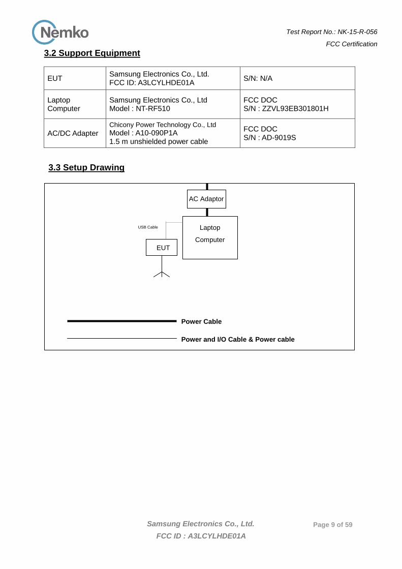
3.3 Setup Drawing
USB Cable
AC Adaptor
EUT
Power Cable
Power and I/O Cable & Power cable
Laptop
Computer
Test Report No.: NK-15-R-056
FCC Certification
Samsung Electronics Co., Ltd. FCC ID : A3LCYLHDE01A
Page 10 of 59
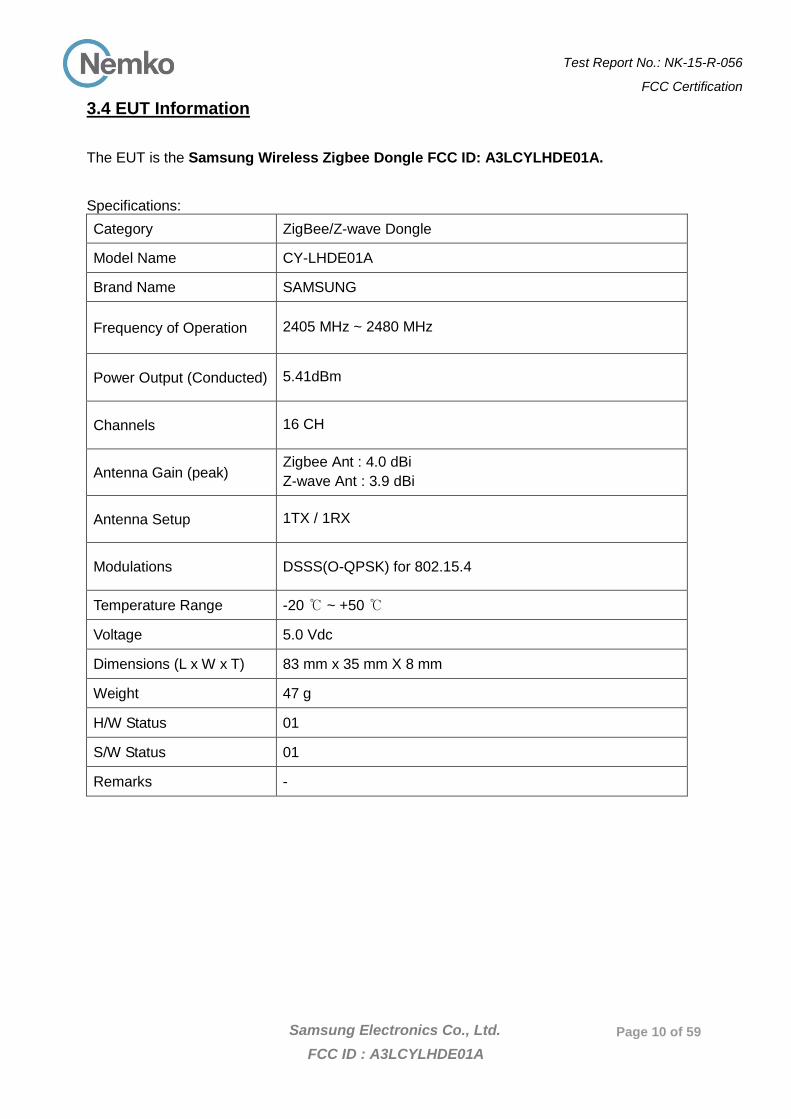
3.4 EUT Information The EUT is the Samsung Wireless Zigbee Dongle FCC ID: A3LCYLHDE01A. Specifications: Category ZigBee/Z-wave Dongle
Model Name CY-LHDE01A
Brand Name SAMSUNG
Frequency of Operation 2405 MHz ~ 2480 MHz
Power Output (Conducted) 5.41dBm
Channels 16 CH
Antenna Gain (peak) Zigbee Ant : 4.0 dBi Z-wave Ant : 3.9 dBi
Antenna Setup 1TX / 1RX
Modulations DSSS(O-QPSK) for 802.15.4
Temperature Range -20 ℃ ~ +50 ℃
Voltage 5.0 Vdc
Dimensions (L x W x T) 83 mm x 35 mm X 8 mm
Weight 47 g
H/W Status 01
S/W Status 01
Remarks -
Test Report No.: NK-15-R-056
FCC Certification
Samsung Electronics Co., Ltd. FCC ID : A3LCYLHDE01A
Page 11 of 59
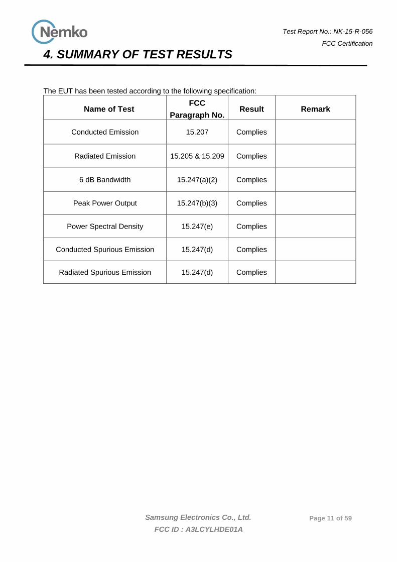
4. SUMMARY OF TEST RESULTS
The EUT has been tested according to the following specification:
Name of Test FCC
Paragraph No. Result Remark
Conducted Emission 15.207 Complies
Radiated Emission 15.205 & 15.209 Complies
6 dB Bandwidth 15.247(a)(2) Complies
Peak Power Output 15.247(b)(3) Complies
Power Spectral Density 15.247(e) Complies
Conducted Spurious Emission 15.247(d) Complies
Radiated Spurious Emission 15.247(d) Complies
Test Report No.: NK-15-R-056
FCC Certification
Samsung Electronics Co., Ltd. FCC ID : A3LCYLHDE01A
Page 12 of 59
5. RECOMMENDATION/CONCLUSION The data collected shows that the Samsung ZigBee/Z-wave Dongle FCC ID:A3LCYLHDE01A is in compliance with Part 15.247 of the FCC Rule. 6. ANTENNA REQUIREMENTS §15.203 of the FCC Rules part 15 Subpart C : An intentional radiator shall be designed to ensure that no antenna other than that furnished by the responsible party shall be used with the device. The use of a permanently attached antenna or of an antenna that uses a unique coupling to the intentional radiator shall be considered sufficient to comply with the provisions of this section. The antenna of the Samsung ZigBee/Z-wave Dongle FCC ID: A3LCYLHDE01A is permanently attached and there are no provisions for connection to an external antenna. It complies with the requirement of §15.203.
Test Report No.: NK-15-R-056
FCC Certification
Samsung Electronics Co., Ltd. FCC ID : A3LCYLHDE01A
Page 13 of 59
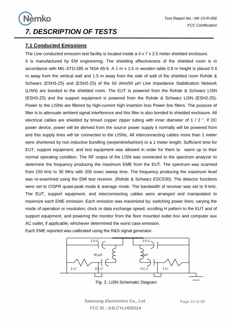
7. DESCRIPTION OF TESTS 7.1 Conducted Emissions The Line conducted emission test facility is located inside a 4 x 7 x 2.5 meter shielded enclosure.
It is manufactured by EM engineering. The shielding effectiveness of the shielded room is in
accordance with MIL-STD-285 or NSA 65-6. A 1 m x 1.5 m wooden table 0.8 m height is placed 0.4
m away from the vertical wall and 1.5 m away from the side of wall of the shielded room Rohde &
Schwarz (ESH3-Z5) and (ESH2-Z5) of the 50 ohm/50 µH Line Impedance Stabilization Network
(LISN) are bonded to the shielded room. The EUT is powered from the Rohde & Schwarz LISN
(ESH3-Z5) and the support equipment is powered from the Rohde & Schwarz LISN (ESH2-Z5).
Power to the LISNs are filtered by high-current high insertion loss Power line filters. The purpose of
filter is to attenuate ambient signal interference and this filter is also bonded to shielded enclosure. All
electrical cables are shielded by tinned copper zipper tubing with inner diameter of 1 / 2 ”. If DC
power device, power will be derived from the source power supply it normally will be powered from
and this supply lines will be connected to the LISNs, All interconnecting cables more than 1 meter
were shortened by non inductive bundling (serpentinefashion) to a 1 meter length. Sufficient time for
EUT, support equipment, and test equipment was allowed in order for them to warm up to their
normal operating condition. The RF output of the LISN was connected to the spectrum analyzer to
determine the frequency producing the maximum EME from the EUT. The spectrum was scanned
from 150 kHz to 30 MHz with 200 msec sweep time. The frequency producing the maximum level
was re-examined using the EMI test receiver. (Rohde & Schwarz ESCS30). The detector functions
were set to CISPR quasi-peak mode & average mode. The bandwidth of receiver was set to 9 kHz.
The EUT, support equipment, and interconnecting cables were arranged and manipulated to
maximize each EME emission. Each emission was maximized by; switching power lines; varying the
mode of operation or resolution; clock or data exchange speed; scrolling H pattern to the EUT and of
support equipment, and powering the monitor from the floor mounted outlet box and computer aux
AC outlet, if applicable; whichever determined the worst case emission.
Each EME reported was calibrated using the R&S signal generator.
1.0㎌ 1.0㎌ 50 µH 50 µH 1㏀ 0.1㎌ 0.1㎌ 1㏀ Fig. 2. LISN Schematic Diagram
Test Report No.: NK-15-R-056
FCC Certification
Samsung Electronics Co., Ltd. FCC ID : A3LCYLHDE01A
Page 14 of 59
7.2 Radiated Emissions The measurement was performed at the test site that is specified in accordance with ANCI C63.10-
2009.
The spurious emission was scanned from 9 kHz to 30 MHz using Loop Antenna(Rohde&Schwarz,
HFH2-Z2) and 30 to 1000 MHz using Trilog broadband test antenna(Schwarzbeck, VULB 9163).
Above 1 GHz, Horn antenna (Schwarzbeck BBHA 9120D: up to 18 GHz, Q-par Angus QSH20S20 :
18 to 26.5 GHz, QSH22K20: up to 40 GHz) was used.
For emissions testing at below 1GHz, The test equipment was placed on turntable with 0.8 m above
ground. For emission measurements above 1 GHz, The test equipment was placed on turntable with
1.5 m above ground. Sufficient time for the EUT, support equipment, and test equipment was allowed
in order for them to warm up to their normal operating condition. The EUT, cable, wire arrangement
and mode of operation that has the highest amplitude relative to the limit was selected. Then, the turn
table was rotated from 0˚ to 360˚ and an antenna mast was moved from 1 m to 4 m height to
maximize the suspected highest amplitude signal. The final maximized level was recorded.
At frequencies below 1000 MHz, measurements performed using the CISPR quasi-peak detection. At
frequencies above 1000 MHz, measurements performed using the peak and average measurement
procedures described in KDB “558074 D01 DTS Meas Guidance v03r03” in section 12.2.4 and
12.2.5.2. Peak emission levels were measured by setting the analyzer RBW = 1 MHz, VBW = 3 MHz,
Detector = Peak, Trace mode = max hold. Average emission levels were measured by setting the
analyzer RBW = 1 MHz, VBW = 3 MHz, Detector = RMS, Trace averaging in power averaging (RMS)
mode over a minimum of 100 traces, when the EUT was configured to transmit with duty cycle ≥ 98
percent. If continuous transmission of the EUT couldn’t be achieved and duty cycle was constant, a
correction factor (10 log (1 / x)) was added to the measurement result.
Frequency (MHz) Field strength (microvolts/meter) Measurement distance (meters)
0.009–0.490 2400/F(kHz) 300 0.490–1.705 24000/F(kHz) 30 1.705–30.0 30 30
30–88 100 3 88–216 150 3
216–960 200 3 Above 960 500 3
Radiated Emissions Limits per 47 CFR 15.209(a)
Note :
*Instead of 0.8m EUT height above 1GHz, 1.5m was used as allowed by FCC December 2014 TCB Conference call.
Test Report No.: NK-15-R-056
FCC Certification
Samsung Electronics Co., Ltd. FCC ID : A3LCYLHDE01A
Page 15 of 59
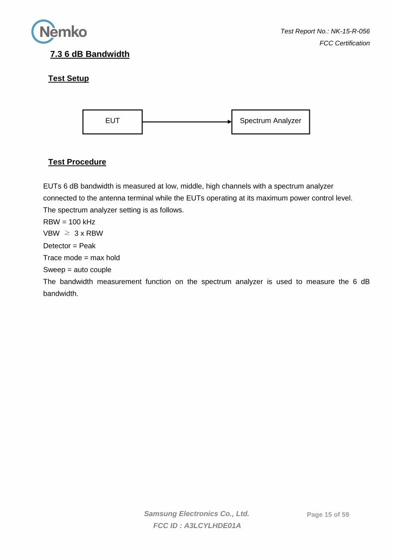
7.3 6 dB Bandwidth
Test Setup
Test Procedure
EUTs 6 dB bandwidth is measured at low, middle, high channels with a spectrum analyzer connected to the antenna terminal while the EUTs operating at its maximum power control level. The spectrum analyzer setting is as follows. RBW = 100 kHz VBW ≥ 3 x RBW
Detector = Peak Trace mode = max hold Sweep = auto couple The bandwidth measurement function on the spectrum analyzer is used to measure the 6 dB bandwidth.
EUT Spectrum Analyzer
Test Report No.: NK-15-R-056
FCC Certification
Samsung Electronics Co., Ltd. FCC ID : A3LCYLHDE01A
Page 16 of 59
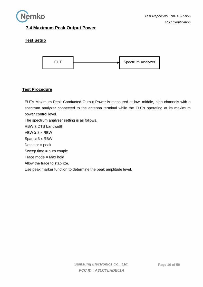
7.4 Maximum Peak Output Power
Test Setup
Test Procedure
EUTs Maximum Peak Conducted Output Power is measured at low, middle, high channels with a spectrum analyzer connected to the antenna terminal while the EUTs operating at its maximum power control level. The spectrum analyzer setting is as follows. RBW ≥ DTS bandwidth VBW ≥ 3 x RBW Span ≥ 3 x RBW Detector = peak Sweep time = auto couple Trace mode = Max hold Allow the trace to stabilize. Use peak marker function to determine the peak amplitude level.
EUT Spectrum Analyzer
Test Report No.: NK-15-R-056
FCC Certification
Samsung Electronics Co., Ltd. FCC ID : A3LCYLHDE01A
Page 17 of 59
7.5 Peak Power Spectral Density
Test Setup
Test Procedure
EUTs Peak Power Spectral Density is measured at low, middle, high channels with a spectrum analyzer connected to the antenna terminal while the EUTs operating at its maximum power control level. The spectrum analyzer setting is as follows. Center frequency = DTS channel center frequency Span = 1.5 times the DTS channel bandwidth RBW to : 3 kHz ≤ RBW ≤ 100 kHz VBW ≥ 3 x RBW Detector = peak Sweep time = auto couple Trace mode = max hold Allow the trace to stabilize. The peak search function on the spectrum analyzer is used to determine the maximum amplitude level within the fundamental DTS bandwidth.
EUT Spectrum Analyzer
Test Report No.: NK-15-R-056
FCC Certification
Samsung Electronics Co., Ltd. FCC ID : A3LCYLHDE01A
Page 18 of 59
7.6 Conducted Spurious Emissions
Test Setup
Test Procedure
EUTs Conducted spurious emissions are measured at low, middle, high channels with a spectrum analyzer connected to the antenna terminal while the EUTs operating at its maximum power control level. The spectrum analyzer setting is as follows. 1) Reference Level Center frequency = DTS channel center frequency Span ≥ 1.5 times the DTS bandwidth
RBW = 100 kHz VBW ≥ 3 x RBW
Detector = peak Sweep time = auto couple Trace mode = max hold Allow trace to fully stabilize. The peak search function on the spectrum analyzer is used to determine the maximum PSD level. 2) Unwanted Emissions Set the center frequency and span to encompass frequency range to be measured. RBW = 100 kHz VBW ≥ 3 x RBW
Detector = peak Sweep time = auto couple Trace mode = max hold Allow trace to fully stabilize. The peak marker function on the spectrum analyzer is used to determine the maximum amplitude level of all unwanted emissions outside of the authorized frequency band. The unwanted emissions are attenuated by at least the minimum requirements specified.
EUT Spectrum Analyzer
Test Report No.: NK-15-R-056
FCC Certification
Samsung Electronics Co., Ltd. FCC ID : A3LCYLHDE01A
Page 19 of 59
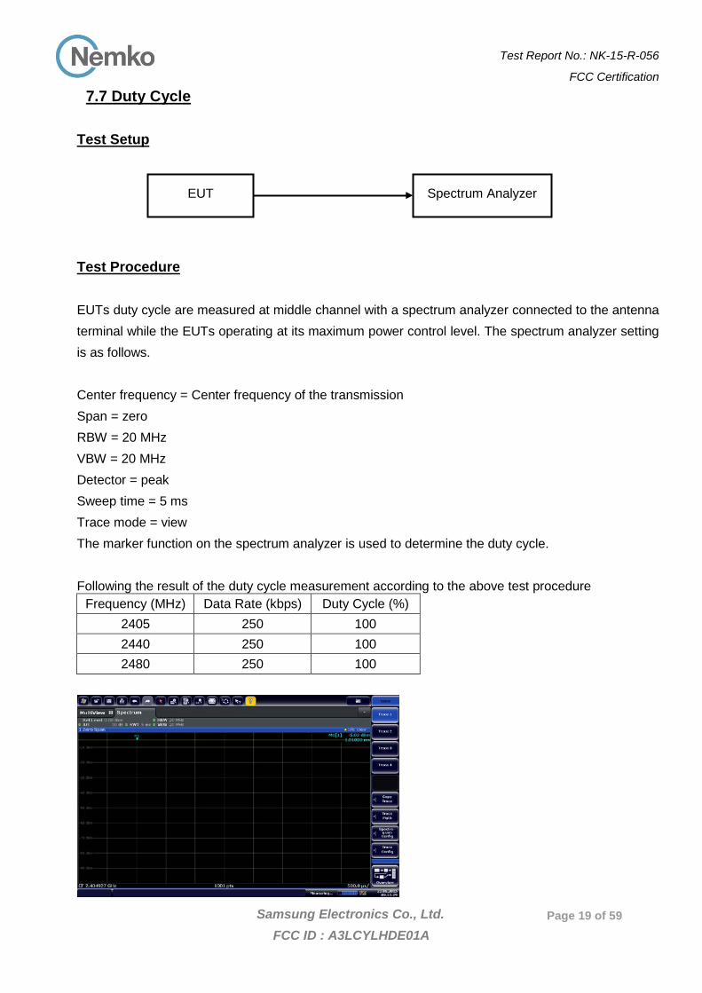
7.7 Duty Cycle
Test Setup
Test Procedure EUTs duty cycle are measured at middle channel with a spectrum analyzer connected to the antenna terminal while the EUTs operating at its maximum power control level. The spectrum analyzer setting is as follows. Center frequency = Center frequency of the transmission Span = zero RBW = 20 MHz VBW = 20 MHz Detector = peak Sweep time = 5 ms Trace mode = view The marker function on the spectrum analyzer is used to determine the duty cycle. Following the result of the duty cycle measurement according to the above test procedure
Frequency (MHz) Data Rate (kbps) Duty Cycle (%) 2405 250 100 2440 250 100 2480 250 100
EUT Spectrum Analyzer
Test Report No.: NK-15-R-056
FCC Certification
Samsung Electronics Co., Ltd. FCC ID : A3LCYLHDE01A
Page 20 of 59
8. TEST DATA
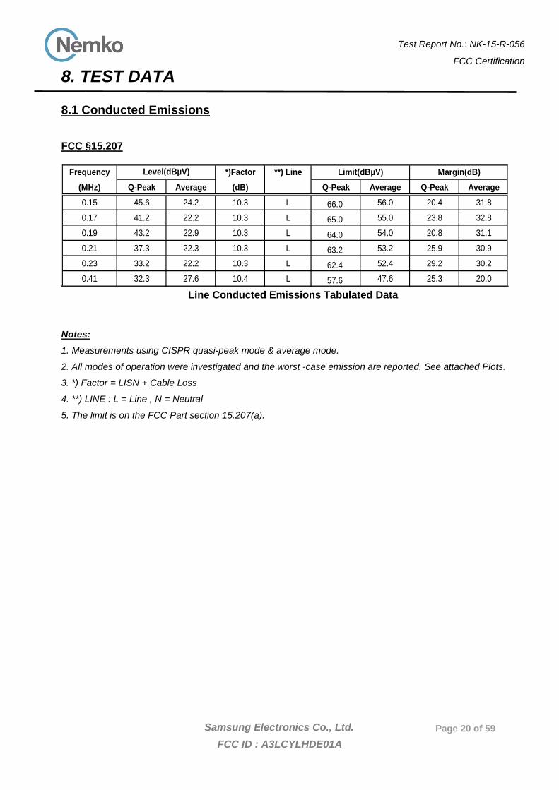
8.1 Conducted Emissions
FCC §15.207
Frequency *)Factor **) Line Limit(dBµV) Margin(dB)(MHz) Q-Peak Average (dB) Q-Peak Average Q-Peak Average0.15 45.6 24.2 10.3 L 66.0 56.0 20.4 31.8
0.17 41.2 22.2 10.3 L 65.0 55.0 23.8 32.8
0.19 43.2 22.9 10.3 L 64.0 54.0 20.8 31.1
0.21 37.3 22.3 10.3 L 63.2 53.2 25.9 30.9
0.23 33.2 22.2 10.3 L 62.4 52.4 29.2 30.2
0.41 32.3 27.6 10.4 L 57.6 47.6 25.3 20.0
Level(dBµV)
Line Conducted Emissions Tabulated Data
Notes: 1. Measurements using CISPR quasi-peak mode & average mode.
2. All modes of operation were investigated and the worst -case emission are reported. See attached Plots.
3. *) Factor = LISN + Cable Loss
4. **) LINE : L = Line , N = Neutral
5. The limit is on the FCC Part section 15.207(a).
Test Report No.: NK-15-R-056
FCC Certification
Samsung Electronics Co., Ltd. FCC ID : A3LCYLHDE01A
Page 21 of 59
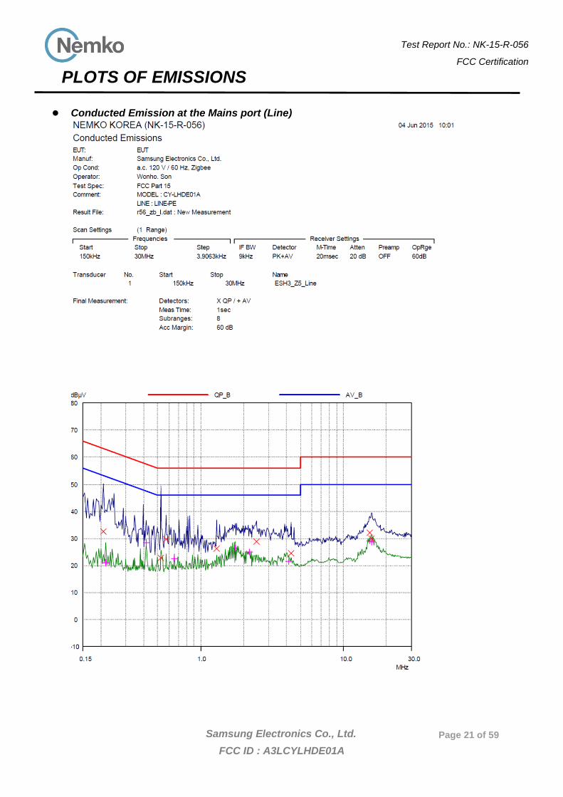
PLOTS OF EMISSIONS
Conducted Emission at the Mains port (Line)
Test Report No.: NK-15-R-056
FCC Certification
Samsung Electronics Co., Ltd. FCC ID : A3LCYLHDE01A
Page 22 of 59
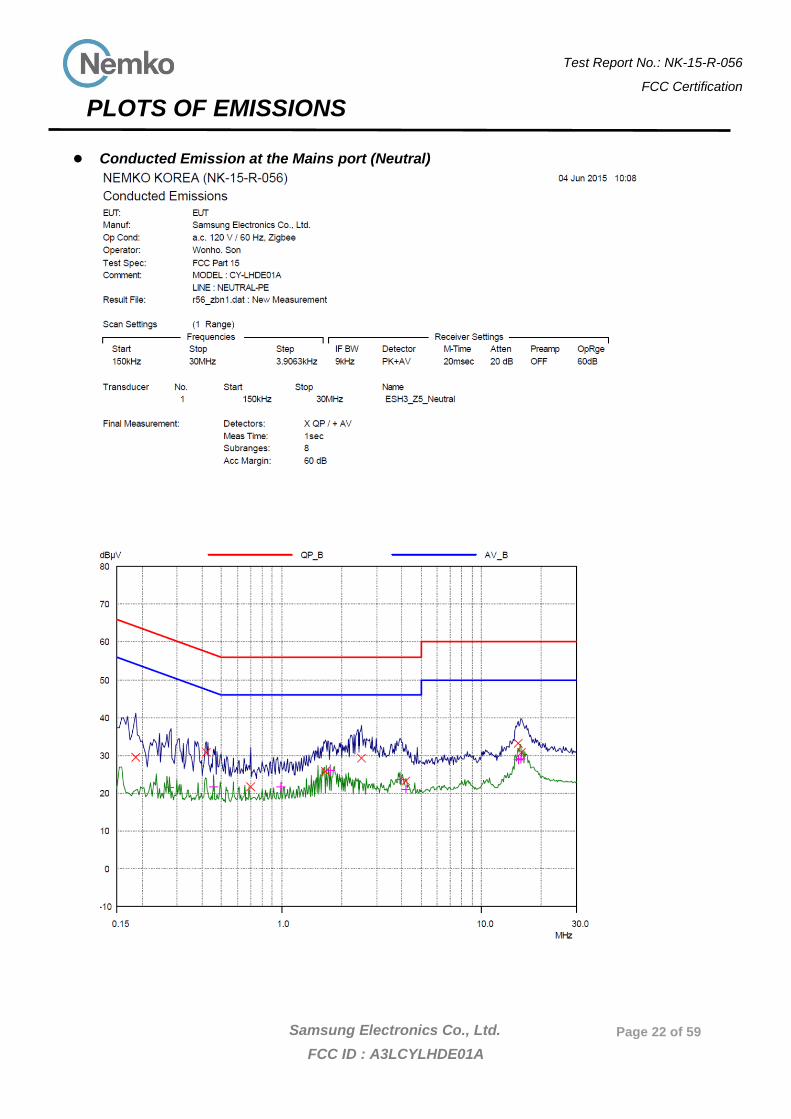
PLOTS OF EMISSIONS
Conducted Emission at the Mains port (Neutral)
Test Report No.: NK-15-R-056
FCC Certification
Samsung Electronics Co., Ltd. FCC ID : A3LCYLHDE01A
Page 23 of 59
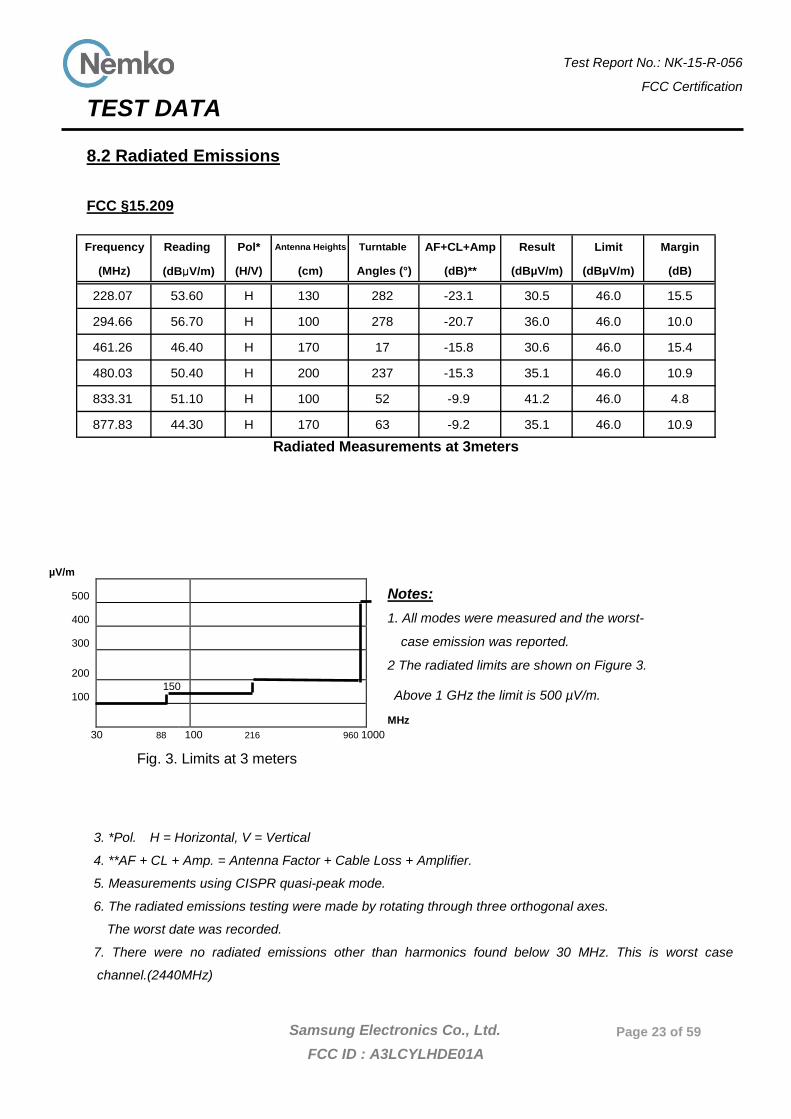
TEST DATA
8.2 Radiated Emissions
FCC §15.209
Frequency Reading Pol* Antenna Heights Turntable AF+CL+Amp Result Limit Margin
(MHz) (dBµV/m) (H/V) (cm) Angles (°) (dB)** (dBµV/m) (dBµV/m) (dB)
228.07 53.60 H 130 282 -23.1 30.5 46.0 15.5
294.66 56.70 H 100 278 -20.7 36.0 46.0 10.0
461.26 46.40 H 170 17 -15.8 30.6 46.0 15.4
480.03 50.40 H 200 237 -15.3 35.1 46.0 10.9
833.31 51.10 H 100 52 -9.9 41.2 46.0 4.8
877.83 44.30 H 170 63 -9.2 35.1 46.0 10.9 Radiated Measurements at 3meters
µV/m 500 Notes:
400 1. All modes were measured and the worst-
300 case emission was reported.
200
2 The radiated limits are shown on Figure 3.
100 150 Above 1 GHz the limit is 500 µV/m.
MHz 30 88 100 216 960 1000
Fig. 3. Limits at 3 meters
3. *Pol. H = Horizontal, V = Vertical
4. **AF + CL + Amp. = Antenna Factor + Cable Loss + Amplifier.
5. Measurements using CISPR quasi-peak mode.
6. The radiated emissions testing were made by rotating through three orthogonal axes.
The worst date was recorded.
7. There were no radiated emissions other than harmonics found below 30 MHz. This is worst case
channel.(2440MHz)
Test Report No.: NK-15-R-056
FCC Certification
Samsung Electronics Co., Ltd. FCC ID : A3LCYLHDE01A
Page 24 of 59
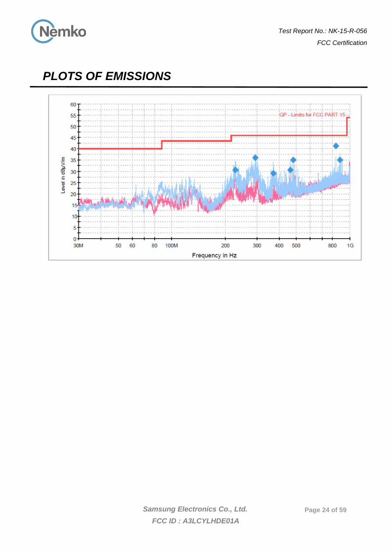
PLOTS OF EMISSIONS
Test Report No.: NK-15-R-056
FCC Certification
Samsung Electronics Co., Ltd. FCC ID : A3LCYLHDE01A
Page 25 of 59
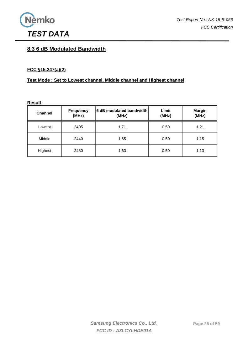
TEST DATA
8.3 6 dB Modulated Bandwidth FCC §15.247(a)(2) Test Mode : Set to Lowest channel, Middle channel and Highest channel Result
Lowest 2405 1.71 0.50 1.21
Middle 2440 1.65 0.50 1.15
Highest 2480 1.63 0.50 1.13
Margin(MHz)
Limit(MHz)Channel Frequency
(MHz)6 dB modulated bandwidth
(MHz)
Test Report No.: NK-15-R-056
FCC Certification
Samsung Electronics Co., Ltd. FCC ID : A3LCYLHDE01A
Page 26 of 59
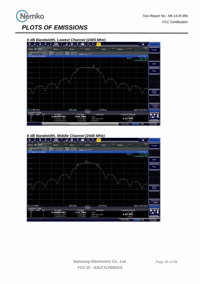
PLOTS OF EMISSIONS
6 dB Bandwidth, Lowest Channel (2405 MHz)
6 dB Bandwidth, Middle Channel (2440 MHz)
Test Report No.: NK-15-R-056
FCC Certification
Samsung Electronics Co., Ltd. FCC ID : A3LCYLHDE01A
Page 27 of 59
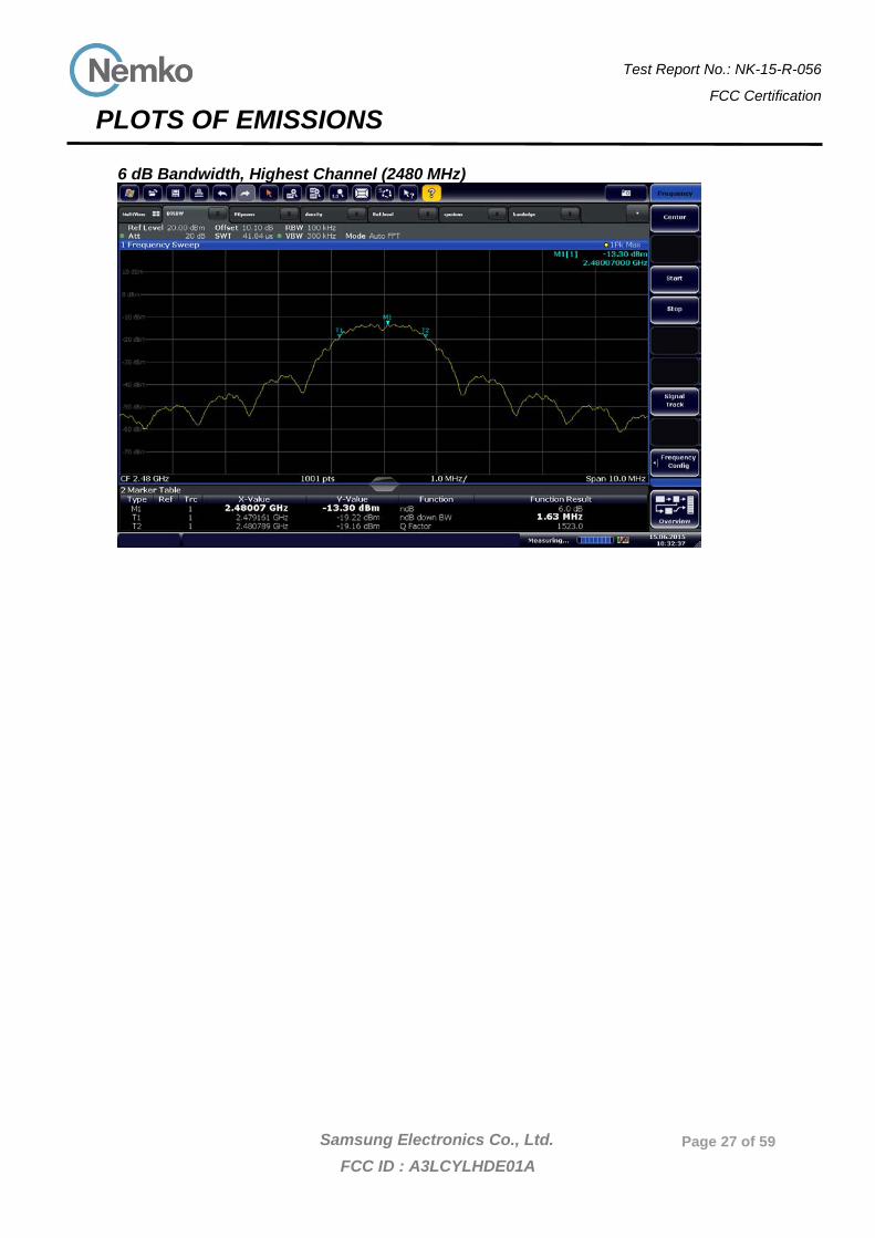
PLOTS OF EMISSIONS
6 dB Bandwidth, Highest Channel (2480 MHz)
Test Report No.: NK-15-R-056
FCC Certification
Samsung Electronics Co., Ltd. FCC ID : A3LCYLHDE01A
Page 28 of 59
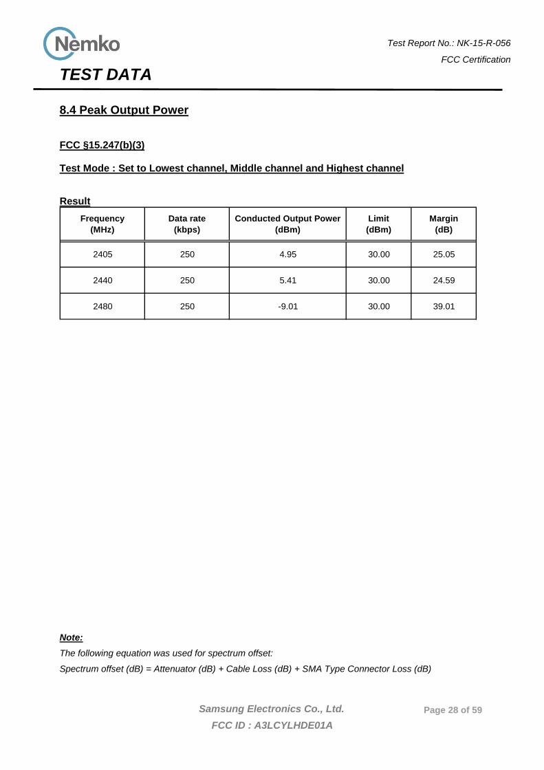
TEST DATA
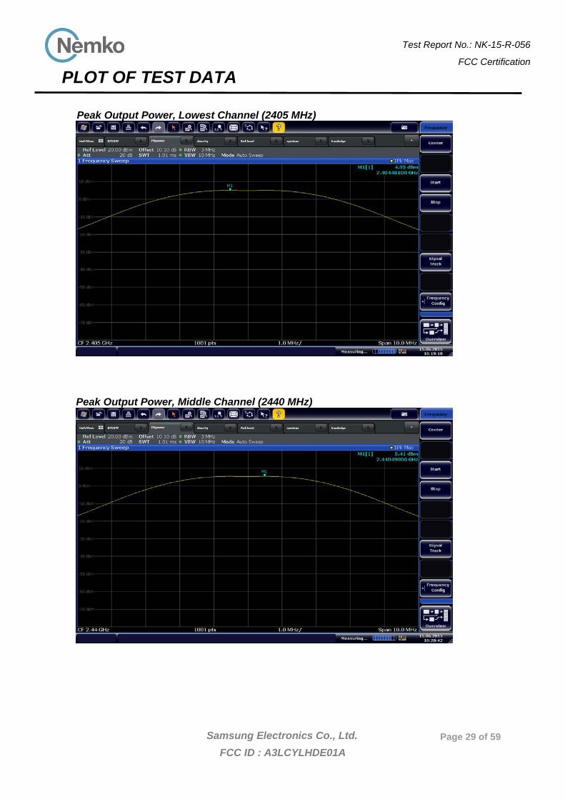
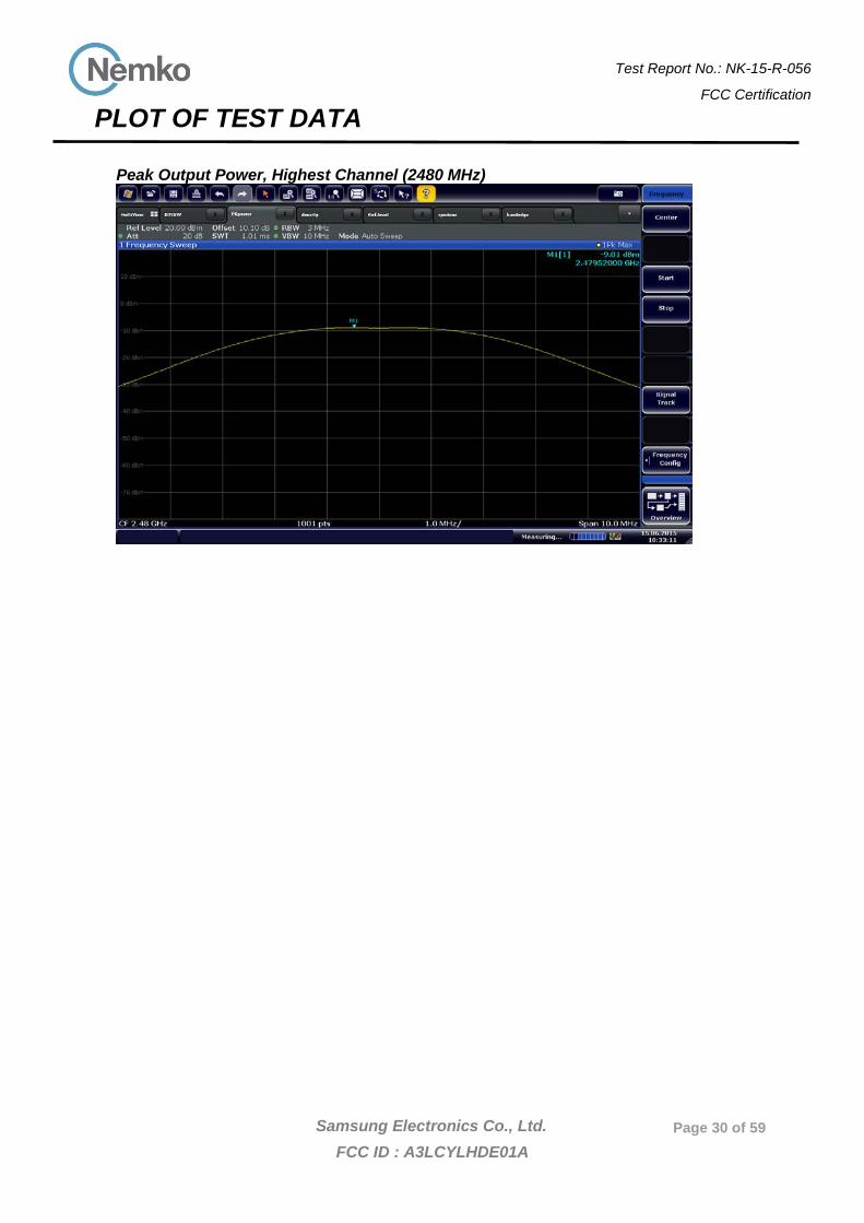
8.4 Peak Output Power
FCC §15.247(b)(3) Test Mode : Set to Lowest channel, Middle channel and Highest channel Result
2405 250 4.95 30.00 25.05
2440 250 5.41 30.00 24.59
2480 250 -9.01 30.00 39.01
Margin(dB)
Limit(dBm)
Frequency(MHz)
Data rate(kbps)
Conducted Output Power(dBm)
Note: The following equation was used for spectrum offset:
Spectrum offset (dB) = Attenuator (dB) + Cable Loss (dB) + SMA Type Connector Loss (dB)
Test Report No.: NK-15-R-056
FCC Certification
Samsung Electronics Co., Ltd. FCC ID : A3LCYLHDE01A
Page 29 of 59
PLOT OF TEST DATA
Peak Output Power, Lowest Channel (2405 MHz)
Peak Output Power, Middle Channel (2440 MHz)
Test Report No.: NK-15-R-056
FCC Certification
Samsung Electronics Co., Ltd. FCC ID : A3LCYLHDE01A
Page 30 of 59
PLOT OF TEST DATA Peak Output Power, Highest Channel (2480 MHz)
Test Report No.: NK-15-R-056
FCC Certification
Samsung Electronics Co., Ltd. FCC ID : A3LCYLHDE01A
Page 31 of 59
TEST DATA
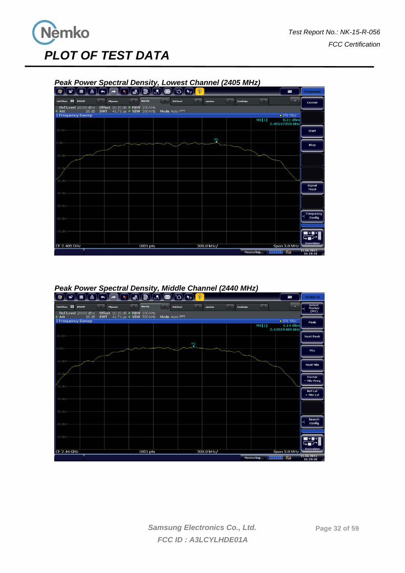
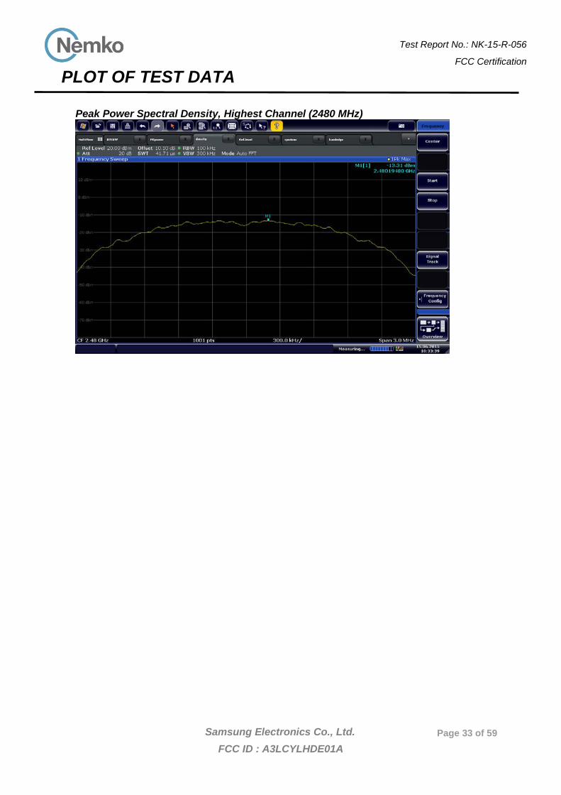
8.5 Peak Power Spectral Density FCC §15.247(e) Test Mode : Set to Lowest channel, Middle channel and Highest channel
Result
Low 2405 8.0
Middle 2440 8.0
High 2480 8.0
1.14
-13.31
Channel Frequency(MHz) Limit (dBm/3kHz)Result(dBm/100kHz)
0.21
Note:
The following equation was used for spectrum offset:
Spectrum offset (dB) = Attenuator (dB) + Cable Loss (dB) + SMA Type Connector Loss (dB)
Test Report No.: NK-15-R-056
FCC Certification
Samsung Electronics Co., Ltd. FCC ID : A3LCYLHDE01A
Page 32 of 59
PLOT OF TEST DATA
Peak Power Spectral Density, Lowest Channel (2405 MHz)
Peak Power Spectral Density, Middle Channel (2440 MHz)
Test Report No.: NK-15-R-056
FCC Certification
Samsung Electronics Co., Ltd. FCC ID : A3LCYLHDE01A
Page 33 of 59
PLOT OF TEST DATA Peak Power Spectral Density, Highest Channel (2480 MHz)
Test Report No.: NK-15-R-056
FCC Certification
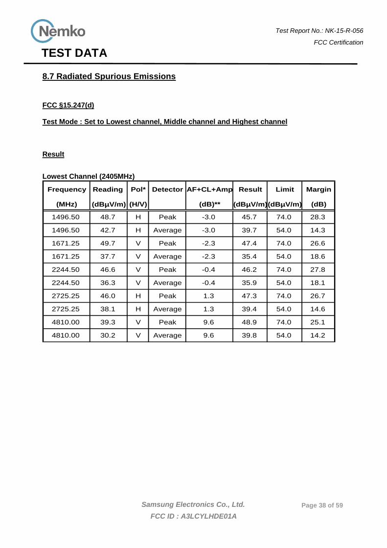
Samsung Electronics Co., Ltd. FCC ID : A3LCYLHDE01A
Page 34 of 59
TEST DATA
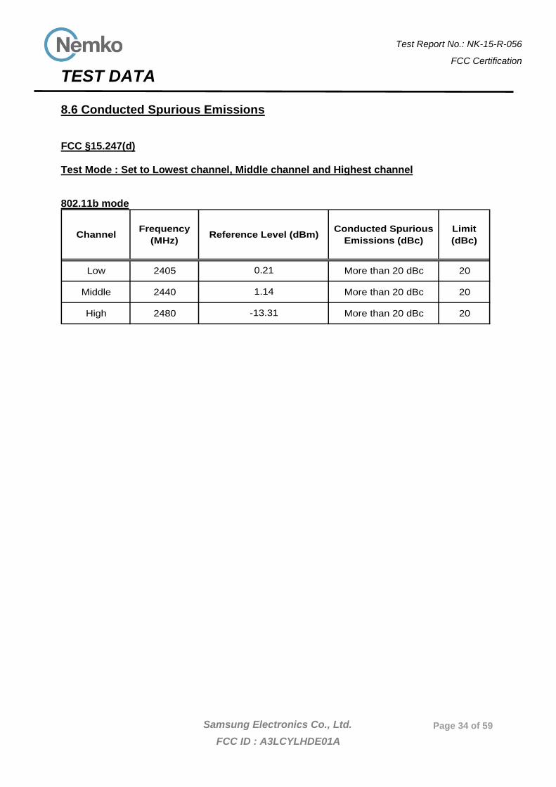
8.6 Conducted Spurious Emissions
FCC §15.247(d) Test Mode : Set to Lowest channel, Middle channel and Highest channel 802.11b mode
Low 2405 More than 20 dBc 20
Middle 2440 More than 20 dBc 20
High 2480 More than 20 dBc 20
Limit(dBc)Reference Level (dBm)
0.21
1.14
-13.31
Channel Frequency(MHz)
Conducted SpuriousEmissions (dBc)
Test Report No.: NK-15-R-056
FCC Certification
Samsung Electronics Co., Ltd. FCC ID : A3LCYLHDE01A
Page 35 of 59
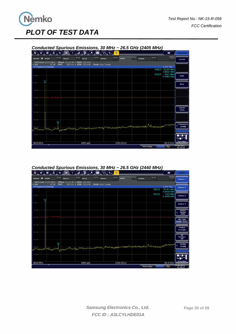
PLOT OF TEST DATA
Conducted Spurious Emissions, 30 MHz ~ 26.5 GHz (2405 MHz)
Conducted Spurious Emissions, 30 MHz ~ 26.5 GHz (2440 MHz)
Test Report No.: NK-15-R-056
FCC Certification
Samsung Electronics Co., Ltd. FCC ID : A3LCYLHDE01A
Page 36 of 59
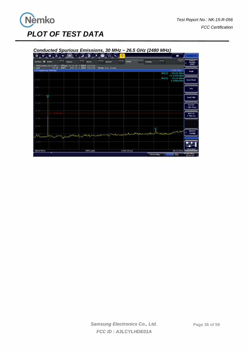
PLOT OF TEST DATA Conducted Spurious Emissions, 30 MHz ~ 26.5 GHz (2480 MHz)
Test Report No.: NK-15-R-056
FCC Certification
Samsung Electronics Co., Ltd. FCC ID : A3LCYLHDE01A
Page 37 of 59
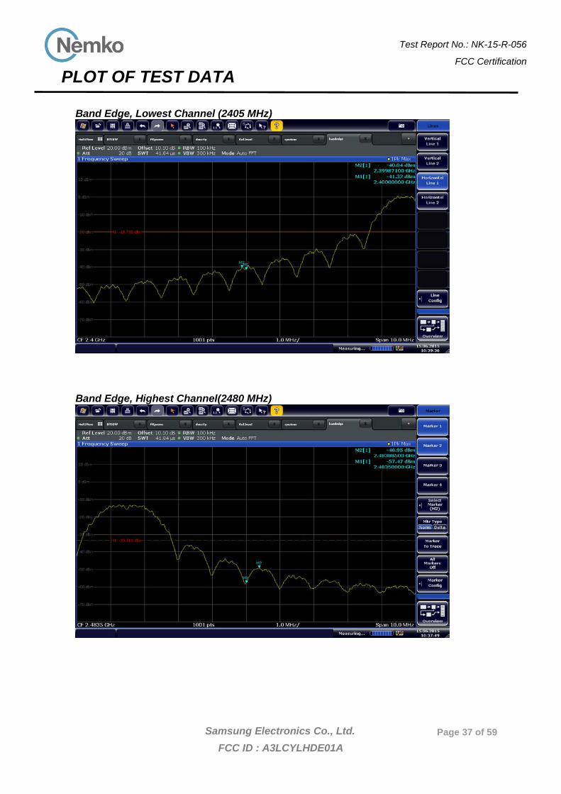
PLOT OF TEST DATA
Band Edge, Lowest Channel (2405 MHz)
Band Edge, Highest Channel(2480 MHz)
Test Report No.: NK-15-R-056
FCC Certification
Samsung Electronics Co., Ltd. FCC ID : A3LCYLHDE01A
Page 38 of 59
TEST DATA
8.7 Radiated Spurious Emissions FCC §15.247(d) Test Mode : Set to Lowest channel, Middle channel and Highest channel Result Lowest Channel (2405MHz)
Frequency Reading Pol* Detector AF+CL+Amp Result Limit Margin
(MHz) (dBμV/m) (H/V) (dB)** (dBμV/m)(dBμV/m) (dB)
1496.50 48.7 H Peak -3.0 45.7 74.0 28.3
1496.50 42.7 H Average -3.0 39.7 54.0 14.3
1671.25 49.7 V Peak -2.3 47.4 74.0 26.6
1671.25 37.7 V Average -2.3 35.4 54.0 18.6
2244.50 46.6 V Peak -0.4 46.2 74.0 27.8
2244.50 36.3 V Average -0.4 35.9 54.0 18.1
2725.25 46.0 H Peak 1.3 47.3 74.0 26.7
2725.25 38.1 H Average 1.3 39.4 54.0 14.6
4810.00 39.3 V Peak 9.6 48.9 74.0 25.1
4810.00 30.2 V Average 9.6 39.8 54.0 14.2
Test Report No.: NK-15-R-056
FCC Certification
Samsung Electronics Co., Ltd. FCC ID : A3LCYLHDE01A
Page 39 of 59
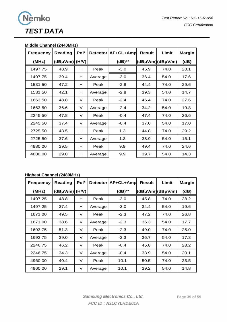
TEST DATA
Middle Channel (2440MHz)
Frequency Reading Pol* Detector AF+CL+Amp Result Limit Margin
(MHz) (dBμV/m) (H/V) (dB)** (dBμV/m)(dBμV/m) (dB)
1497.75 48.9 H Peak -3.0 45.9 74.0 28.1
1497.75 39.4 H Average -3.0 36.4 54.0 17.6
1531.50 47.2 H Peak -2.8 44.4 74.0 29.6
1531.50 42.1 H Average -2.8 39.3 54.0 14.7
1663.50 48.8 V Peak -2.4 46.4 74.0 27.6
1663.50 36.6 V Average -2.4 34.2 54.0 19.8
2245.50 47.8 V Peak -0.4 47.4 74.0 26.6
2245.50 37.4 V Average -0.4 37.0 54.0 17.0
2725.50 43.5 H Peak 1.3 44.8 74.0 29.2
2725.50 37.6 H Average 1.3 38.9 54.0 15.1
4880.00 39.5 H Peak 9.9 49.4 74.0 24.6
4880.00 29.8 H Average 9.9 39.7 54.0 14.3
Highest Channel (2480MHz)
Frequency Reading Pol* Detector AF+CL+Amp Result Limit Margin
(MHz) (dBμV/m) (H/V) (dB)** (dBμV/m)(dBμV/m) (dB)
1497.25 48.8 H Peak -3.0 45.8 74.0 28.2
1497.25 37.4 H Average -3.0 34.4 54.0 19.6
1671.00 49.5 V Peak -2.3 47.2 74.0 26.8
1671.00 38.6 V Average -2.3 36.3 54.0 17.7
1693.75 51.3 V Peak -2.3 49.0 74.0 25.0
1693.75 39.0 V Average -2.3 36.7 54.0 17.3
2246.75 46.2 V Peak -0.4 45.8 74.0 28.2
2246.75 34.3 V Average -0.4 33.9 54.0 20.1
4960.00 40.4 V Peak 10.1 50.5 74.0 23.5
4960.00 29.1 V Average 10.1 39.2 54.0 14.8
Test Report No.: NK-15-R-056
FCC Certification
Samsung Electronics Co., Ltd. FCC ID : A3LCYLHDE01A
Page 40 of 59
Note(s): 1. *Pol. H = Horizontal V = Vertical
2. **AF + CL + Amp. = Antenna Factor + Cable Loss + Amplifier.
3. The radiated emissions testing were made by rotating EUT through three orthogonal axes and rotating the
receive antenna with horizontal, Vertical polarization. The worst data was recorded.
4. Peak emissions were measured using RBW = 1 MHz, VBW = 3 MHz, Detector = Peak
5. For average measurements, “12.2.5.1 Average Power Measurement Procedures” at “558074 D01 DTS
Meas Guidance v03r03” was used.
6. The spectrum was measured from 9 kHz to 10th harmonic and the worst-case emissions were reported. No
significant emissions were found beyond the 2nd harmonic for this device.
Test Report No.: NK-15-R-056
FCC Certification
Samsung Electronics Co., Ltd. FCC ID : A3LCYLHDE01A
Page 41 of 59
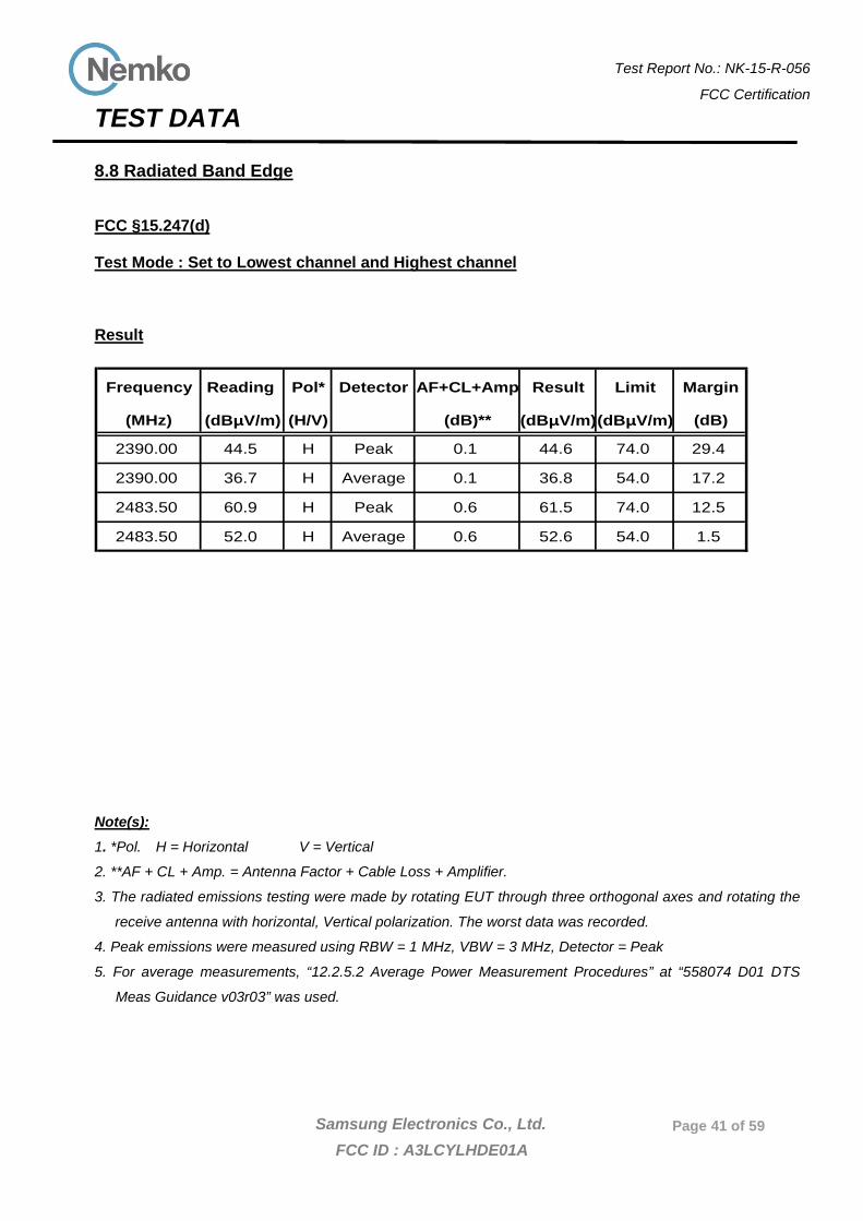
TEST DATA
8.8 Radiated Band Edge
FCC §15.247(d) Test Mode : Set to Lowest channel and Highest channel Result
Frequency Reading Pol* Detector AF+CL+Amp Result Limit Margin
(MHz) (dBμV/m) (H/V) (dB)** (dBμV/m)(dBμV/m) (dB)
2390.00 44.5 H Peak 0.1 44.6 74.0 29.4
2390.00 36.7 H Average 0.1 36.8 54.0 17.2
2483.50 60.9 H Peak 0.6 61.5 74.0 12.5
2483.50 52.0 H Average 0.6 52.6 54.0 1.5
Note(s): 1. *Pol. H = Horizontal V = Vertical
2. **AF + CL + Amp. = Antenna Factor + Cable Loss + Amplifier.
3. The radiated emissions testing were made by rotating EUT through three orthogonal axes and rotating the
receive antenna with horizontal, Vertical polarization. The worst data was recorded.
4. Peak emissions were measured using RBW = 1 MHz, VBW = 3 MHz, Detector = Peak
5. For average measurements, “12.2.5.2 Average Power Measurement Procedures” at “558074 D01 DTS
Meas Guidance v03r03” was used.
Test Report No.: NK-15-R-056
FCC Certification
Samsung Electronics Co., Ltd. FCC ID : A3LCYLHDE01A
Page 42 of 59
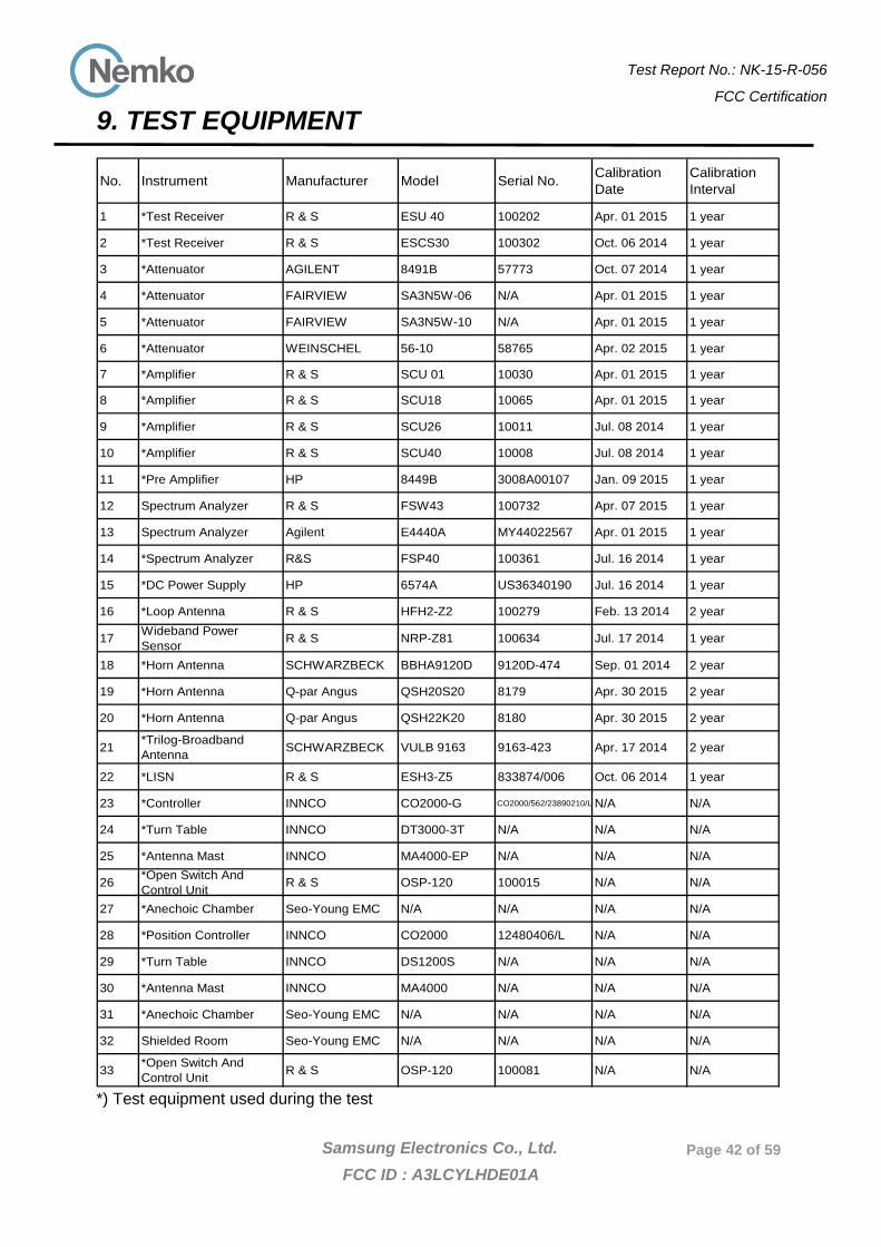
9. TEST EQUIPMENT
No. Instrument Manufacturer Model Serial No. CalibrationDate
CalibrationInterval
1 *Test Receiver R & S ESU 40 100202 Apr. 01 2015 1 year
2 *Test Receiver R & S ESCS30 100302 Oct. 06 2014 1 year
3 *Attenuator AGILENT 8491B 57773 Oct. 07 2014 1 year
4 *Attenuator FAIRVIEW SA3N5W-06 N/A Apr. 01 2015 1 year
5 *Attenuator FAIRVIEW SA3N5W-10 N/A Apr. 01 2015 1 year
6 *Attenuator WEINSCHEL 56-10 58765 Apr. 02 2015 1 year
7 *Amplifier R & S SCU 01 10030 Apr. 01 2015 1 year
8 *Amplifier R & S SCU18 10065 Apr. 01 2015 1 year
9 *Amplifier R & S SCU26 10011 Jul. 08 2014 1 year
10 *Amplifier R & S SCU40 10008 Jul. 08 2014 1 year
11 *Pre Amplifier HP 8449B 3008A00107 Jan. 09 2015 1 year
12 Spectrum Analyzer R & S FSW43 100732 Apr. 07 2015 1 year
13 Spectrum Analyzer Agilent E4440A MY44022567 Apr. 01 2015 1 year
14 *Spectrum Analyzer R&S FSP40 100361 Jul. 16 2014 1 year
15 *DC Power Supply HP 6574A US36340190 Jul. 16 2014 1 year
16 *Loop Antenna R & S HFH2-Z2 100279 Feb. 13 2014 2 year
17 Wideband PowerSensor R & S NRP-Z81 100634 Jul. 17 2014 1 year
18 *Horn Antenna SCHWARZBECK BBHA9120D 9120D-474 Sep. 01 2014 2 year
19 *Horn Antenna Q-par Angus QSH20S20 8179 Apr. 30 2015 2 year
20 *Horn Antenna Q-par Angus QSH22K20 8180 Apr. 30 2015 2 year
21 *Trilog-BroadbandAntenna SCHWARZBECK VULB 9163 9163-423 Apr. 17 2014 2 year
22 *LISN R & S ESH3-Z5 833874/006 Oct. 06 2014 1 year
23 *Controller INNCO CO2000-G CO2000/562/23890210/L N/A N/A
24 *Turn Table INNCO DT3000-3T N/A N/A N/A
25 *Antenna Mast INNCO MA4000-EP N/A N/A N/A
26 *Open Switch AndControl Unit R & S OSP-120 100015 N/A N/A
27 *Anechoic Chamber Seo-Young EMC N/A N/A N/A N/A
28 *Position Controller INNCO CO2000 12480406/L N/A N/A
29 *Turn Table INNCO DS1200S N/A N/A N/A
30 *Antenna Mast INNCO MA4000 N/A N/A N/A
31 *Anechoic Chamber Seo-Young EMC N/A N/A N/A N/A
32 Shielded Room Seo-Young EMC N/A N/A N/A N/A
33 *Open Switch AndControl Unit R & S OSP-120 100081 N/A N/A
*) Test equipment used during the test
Test Report No.: NK-15-R-056
FCC Certification
Samsung Electronics Co., Ltd. FCC ID : A3LCYLHDE01A
Page 43 of 59
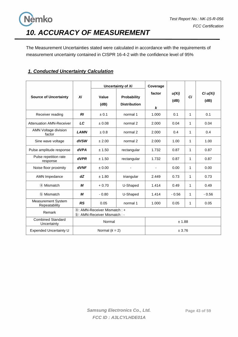
10. ACCURACY OF MEASUREMENT
The Measurement Uncertainties stated were calculated in accordance with the requirements of measurement uncertainty contained in CISPR 16-4-2 with the confidence level of 95%
1. Conducted Uncertainty Calculation
Source of Uncertainty Xi
Uncertainty of Xi Coverage
factor
k
u(Xi)
(dB) Ci
Ci u(Xi)
(dB) Value
(dB)
Probability
Distribution
Receiver reading RI ± 0.1 normal 1 1.000 0.1 1 0.1
Attenuation AMN-Receiver LC ± 0.08 normal 2 2.000 0.04 1 0.04
AMN Voltage division factor LAMN ± 0.8 normal 2 2.000 0.4 1 0.4
Sine wave voltage dVSW ± 2.00 normal 2 2.000 1.00 1 1.00
Pulse amplitude response dVPA ± 1.50 rectangular 1.732 0.87 1 0.87
Pulse repetition rate response dVPR ± 1.50 rectangular 1.732 0.87 1 0.87
Noise floor proximity dVNF ± 0.00 - - 0.00 1 0.00
AMN Impedance dZ ± 1.80 triangular 2.449 0.73 1 0.73
ⓐ Mismatch M + 0.70 U-Shaped 1.414 0.49 1 0.49
ⓑ Mismatch M - 0.80 U-Shaped 1.414 - 0.56 1 - 0.56
Measurement System Repeatability RS 0.05 normal 1 1.000 0.05 1 0.05
Remark ⓐ: AMN-Receiver Mismatch : + ⓑ: AMN-Receiver Mismatch : -
Combined Standard Uncertainty Normal ± 1.88
Expended Uncertainty U Normal (k = 2) ± 3.76
Test Report No.: NK-15-R-056
FCC Certification
Samsung Electronics Co., Ltd. FCC ID : A3LCYLHDE01A
Page 44 of 59
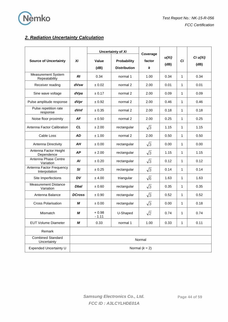
2. Radiation Uncertainty Calculation
Source of Uncertainty Xi
Uncertainty of Xi Coverage
factor
k
u(Xi)
(dB) Ci
Ci u(Xi)
(dB) Value
(dB)
Probability
Distribution
Measurement System Repeatability RI 0.34 normal 1 1.00 0.34 1 0.34
Receiver reading dVsw ± 0.02 normal 2 2.00 0.01 1 0.01
Sine wave voltage dVpa ± 0.17 normal 2 2.00 0.09 1 0.09
Pulse amplitude response dVpr ± 0.92 normal 2 2.00 0.46 1 0.46
Pulse repetition rate response dVnf ± 0.35 normal 2 2.00 0.18 1 0.18
Noise floor proximity AF ± 0.50 normal 2 2.00 0.25 1 0.25
Antenna Factor Calibration CL ± 2.00 rectangular 3 1.15 1 1.15
Cable Loss AD ± 1.00 normal 2 2.00 0.50 1 0.50
Antenna Directivity AH ± 0.00 rectangular 3 0.00 1 0.00
Antenna Factor Height Dependence AP ± 2.00 rectangular 3 1.15 1 1.15
Antenna Phase Centre Variation AI ± 0.20 rectangular 3 0.12 1 0.12
Antenna Factor Frequency Interpolation SI ± 0.25 rectangular 3 0.14 1 0.14
Site Imperfections DV ± 4.00 triangular 6 1.63 1 1.63
Measurement Distance Variation Dbal ± 0.60 rectangular 3 0.35 1 0.35
Antenna Balance DCross ± 0.90 rectangular 3 0.52 1 0.52
Cross Polarisation M ± 0.00 rectangular 3 0.00 1 0.18
Mismatch M + 0.98 - 1.11
U-Shaped 2 0.74 1 0.74
EUT Volume Diameter M 0.33 normal 1 1.00 0.33 1 0.11
Remark
Combined Standard Uncertainty Normal
Expended Uncertainty U Normal (k = 2)