Embed Size (px)
Citation preview
Test Report PMP9491
1 01/15/2015
Test Data For PMP9491
01/19/2015
Test Report PMP9491
2 01/15/2015
Table of Contents 1. Design Specifications ....................................................................................................................... 3
2. Circuit Description ........................................................................................................................... 3
3. PMP9491 Board Photos ................................................................................................................... 4
4. DC/DC Boost Test Results................................................................................................................. 6
4.1 Thermal Data ................................................................................................................................. 6
4.2 Efficiency ....................................................................................................................................... 7
4.2.1 Efficiency Chart ........................................................................................................................... 7
4.2.2 Efficiency Data ............................................................................................................................ 8
4.3 Waveforms .................................................................................................................................. 10
4.3.1 Load Transient Response .......................................................................................................... 10
4.3.2 Startup ...................................................................................................................................... 13
4.3.3 Output Voltage Ripple and Switch Node Voltage ....................................................................... 18
5. Audio Power Amplifier’s Test Result and Jumper Connections ......................................................... 21
5.1 Jumper Connections .................................................................................................................... 21
5.2 BTL: Stereo Waveforms ................................................................................................................ 23
5.2.1 Input /Output Audio ................................................................................................................. 23
5.2.2 All output Audio Signals ............................................................................................................ 24
5.2.3 THD Vs Power: BTL mode .......................................................................................................... 25
5.2.4 THD Vs Frequency: BTL mode .................................................................................................... 26
5.3 PBTL: Woofer Waveforms ............................................................................................................ 27
5.3.1 Input /Output Audio Signals ...................................................................................................... 27
5.3.2 THD Vs Power: PBTL into 2 Ohm ............................................................................................... 32
6. Lithium Battery Charger’s Test Result and Jumper Connections ........................................................ 33
6.1 Jumper Connections .................................................................................................................... 33
6.2 Charging Current and Switch Waveform ...................................................................................... 34
6.3 Transition on Vsystem between Vinput and Battery Voltage ........................................................ 35

Test Report PMP9491
3 01/15/2015
1. Design Specifications
Vin Minimum 3.5V Vin Maximum 10V Vin Nominal 3.6V or 7.2V (Depending on Single or Dual Li ion
Battery) Vout 12VDC Iout 2.5A Switching Frequency(SMPS) 300KHz Audio Amplifier Total Power 30W Audio Amp Output 15W +15W Stereo(on 4 ohm BTL) or 30W Woofer
(on 2 ohm PBTL) Audio Amp Input Stereo Inputs. Processing for Woofer Amp Built-in Li ion Battery Charger –Charge Current 2A max (Adjustable through Resistance) Li ion Battery Charger –Input Current Limit 2A
2. Circuit Description PMP9491 is a 30W Audio Boom Box Design which can be used in 15W +15W Stereo or 30W Woofer Applications. The design is broadly divided into four main stages:
1. Single-Phase Non Synchronous Boost Converter using the LM3481 controller IC. The design accepts an input voltage of 3.3Vin to 10Vin (7.2 VIN Nominal) and provides an output of 12V capable of supplying 2.5A of continuous current to the load.
2. 15W + 15W Stereo Audio Amplifier with TPA3130D2 Class D device.
3. BQ24133- Switch-Mode Li-Ion and Li-Polymer Stand-Alone Battery Charger with Integrated MOSFETs and Power Path Selector capable of Charging 1-3 Cells at 2A.
4. Stereo Inputs to Woofer Bass Input Conversion.

Test Report PMP9491
4 01/15/2015
3. PMP9491 Board Photos Board Dimensions: 5750mil *4970mil
Board Photo (Top)

Test Report PMP9491
5 01/15/2015
Board Photo (Bottom)

Test Report PMP9491
6 01/15/2015
4. DC/DC Boost Test Results
4.1 Thermal Data
IR thermal image taken at steady state with 4.8 Vin and 12V@ 2.5 A load (no airflow)-Boost only
Test Report PMP9491
7 01/15/2015
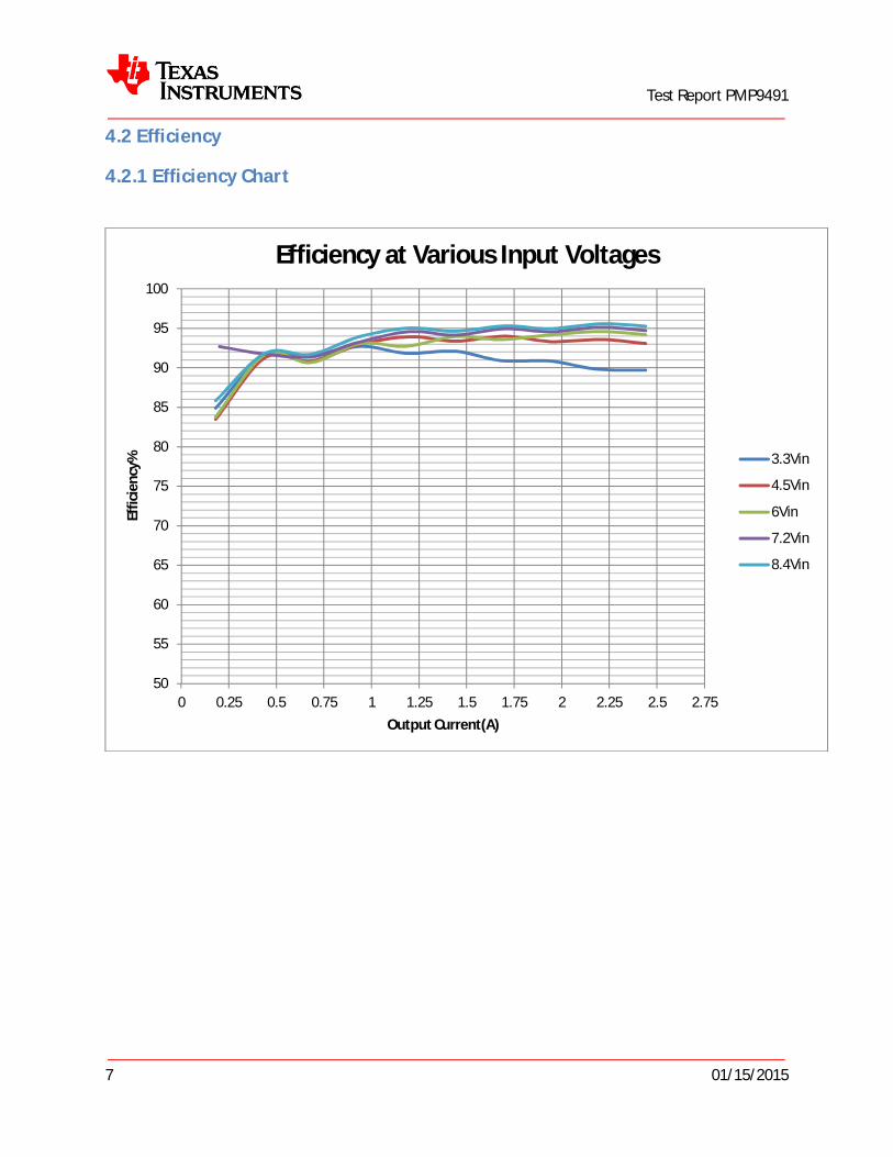
4.2 Efficiency
4.2.1 Efficiency Chart
50
55
60
65
70
75
80
85
90
95
100
0 0.25 0.5 0.75 1 1.25 1.5 1.75 2 2.25 2.5 2.75
Effic
ienc
y%
Output Current(A)
Efficiency at Various Input Voltages
3.3Vin
4.5Vin
6Vin
7.2Vin
8.4Vin

Test Report PMP9491
8 01/15/2015
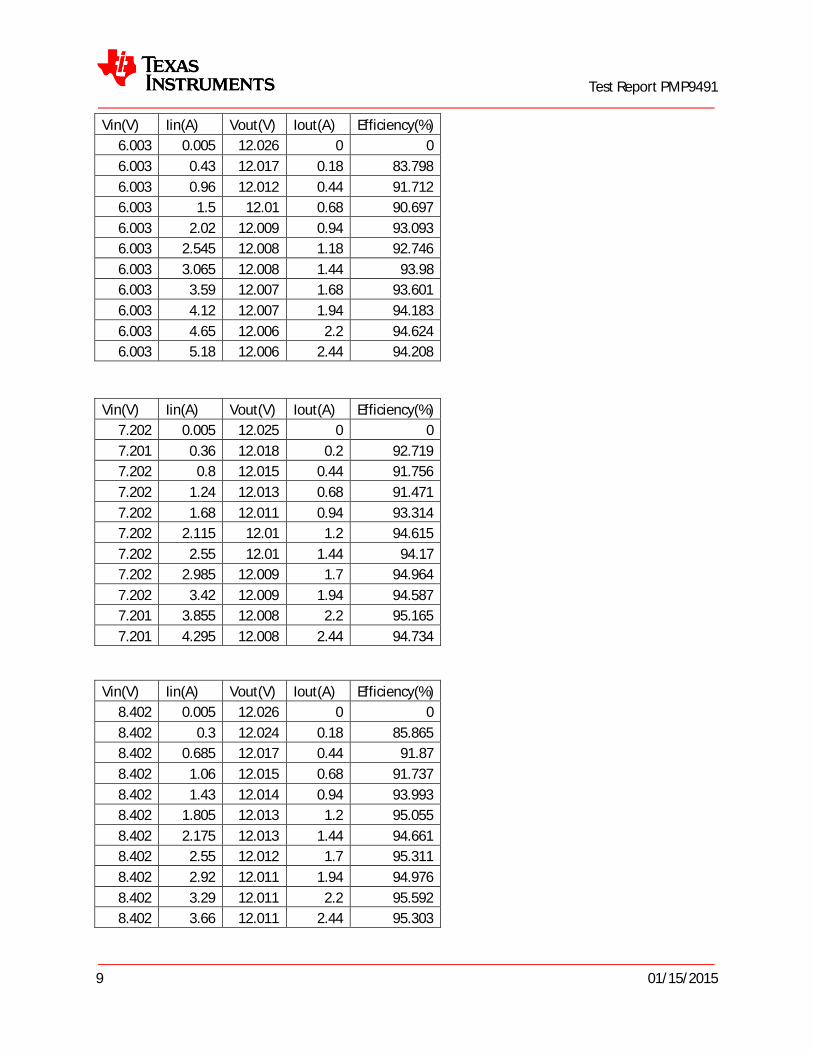
4.2.2 Efficiency Data
Vin(V) Iin(A) Vout(V) Iout(A) Efficiency(%) 3.203 0.01 12.029 0 0 3.203 0.795 12.013 0.18 84.918 3.203 1.8 12.01 0.44 91.657 3.203 2.79 12.009 0.68 91.381 3.203 3.8 12.008 0.94 92.738 3.203 4.815 12.007 1.18 91.868 3.203 5.86 12.006 1.44 92.11 3.203 6.925 12.006 1.68 90.935 3.203 8 12.005 1.94 90.89 3.202 9.095 12.004 2.18 89.858 3.203 10.19 12.003 2.44 89.732
Vin(V) Iin(A) Vout(V) Iout(A) Efficiency(%) 4.504 0.01 12.026 0 0 4.503 0.575 12.013 0.18 83.513 4.503 1.285 12.008 0.44 91.31 4.503 1.995 12.007 0.68 90.886 4.503 2.695 12.006 0.94 92.996 4.503 3.405 12.006 1.2 93.964 4.503 4.11 12.005 1.44 93.407 4.503 4.82 12.004 1.7 94.021 4.503 5.54 12.004 1.94 93.35 4.503 6.265 12.003 2.2 93.603 4.503 6.985 12.003 2.44 93.113
Test Report PMP9491
9 01/15/2015
Vin(V) Iin(A) Vout(V) Iout(A) Efficiency(%) 6.003 0.005 12.026 0 0 6.003 0.43 12.017 0.18 83.798 6.003 0.96 12.012 0.44 91.712 6.003 1.5 12.01 0.68 90.697 6.003 2.02 12.009 0.94 93.093 6.003 2.545 12.008 1.18 92.746 6.003 3.065 12.008 1.44 93.98 6.003 3.59 12.007 1.68 93.601 6.003 4.12 12.007 1.94 94.183 6.003 4.65 12.006 2.2 94.624 6.003 5.18 12.006 2.44 94.208
Vin(V) Iin(A) Vout(V) Iout(A) Efficiency(%)
7.202 0.005 12.025 0 0 7.201 0.36 12.018 0.2 92.719 7.202 0.8 12.015 0.44 91.756 7.202 1.24 12.013 0.68 91.471 7.202 1.68 12.011 0.94 93.314 7.202 2.115 12.01 1.2 94.615 7.202 2.55 12.01 1.44 94.17 7.202 2.985 12.009 1.7 94.964 7.202 3.42 12.009 1.94 94.587 7.201 3.855 12.008 2.2 95.165 7.201 4.295 12.008 2.44 94.734
Vin(V) Iin(A) Vout(V) Iout(A) Efficiency(%) 8.402 0.005 12.026 0 0 8.402 0.3 12.024 0.18 85.865 8.402 0.685 12.017 0.44 91.87 8.402 1.06 12.015 0.68 91.737 8.402 1.43 12.014 0.94 93.993 8.402 1.805 12.013 1.2 95.055 8.402 2.175 12.013 1.44 94.661 8.402 2.55 12.012 1.7 95.311 8.402 2.92 12.011 1.94 94.976 8.402 3.29 12.011 2.2 95.592 8.402 3.66 12.011 2.44 95.303

Test Report PMP9491
10 01/15/2015
4.3 Waveforms
4.3.1 Load Transient Response
Load Transient Response at 3.5Vin and 40%-to-100% (1A-to-2.5A) Load Step
C4- Iout
C3- Vout(AC coupled)

Test Report PMP9491
11 01/15/2015
Load Transient Response at 6Vin and 40%-to-100% (1A-to-2.5A) Load Step
C4- Iout
C3- Vout(AC coupled)
Test Report PMP9491
12 01/15/2015
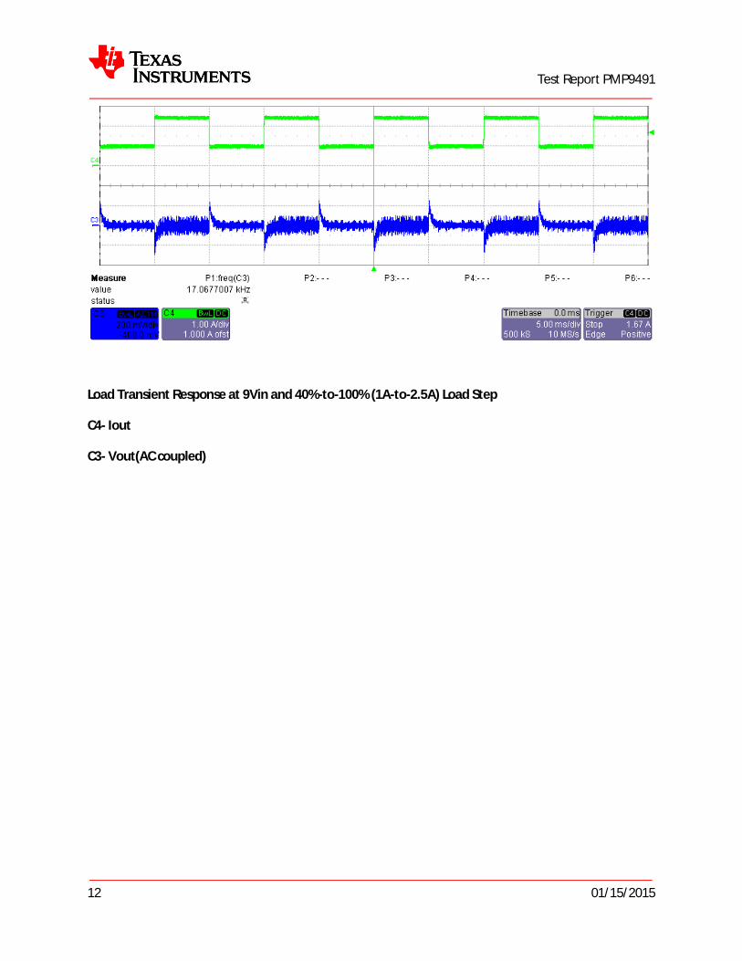
Load Transient Response at 9Vin and 40%-to-100% (1A-to-2.5A) Load Step
C4- Iout
C3- Vout(AC coupled)

Test Report PMP9491
13 01/15/2015
4.3.2 Startup
Startup into No Load at 3.5Vin
C1- Vin
C2-Vout
Test Report PMP9491
14 01/15/2015
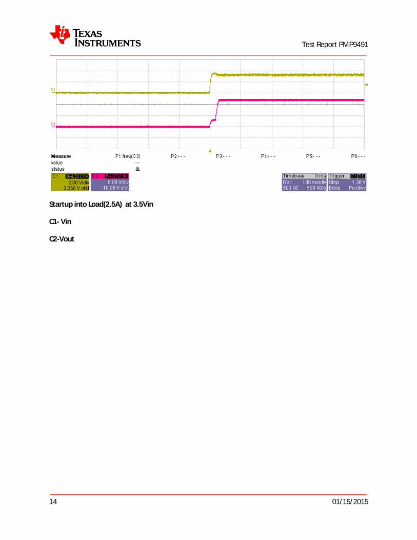
Startup into Load(2.5A) at 3.5Vin
C1- Vin
C2-Vout

Test Report PMP9491
15 01/15/2015
Startup into No Load at 6 Vin
C1- Vin
C2-Vout
Test Report PMP9491
16 01/15/2015
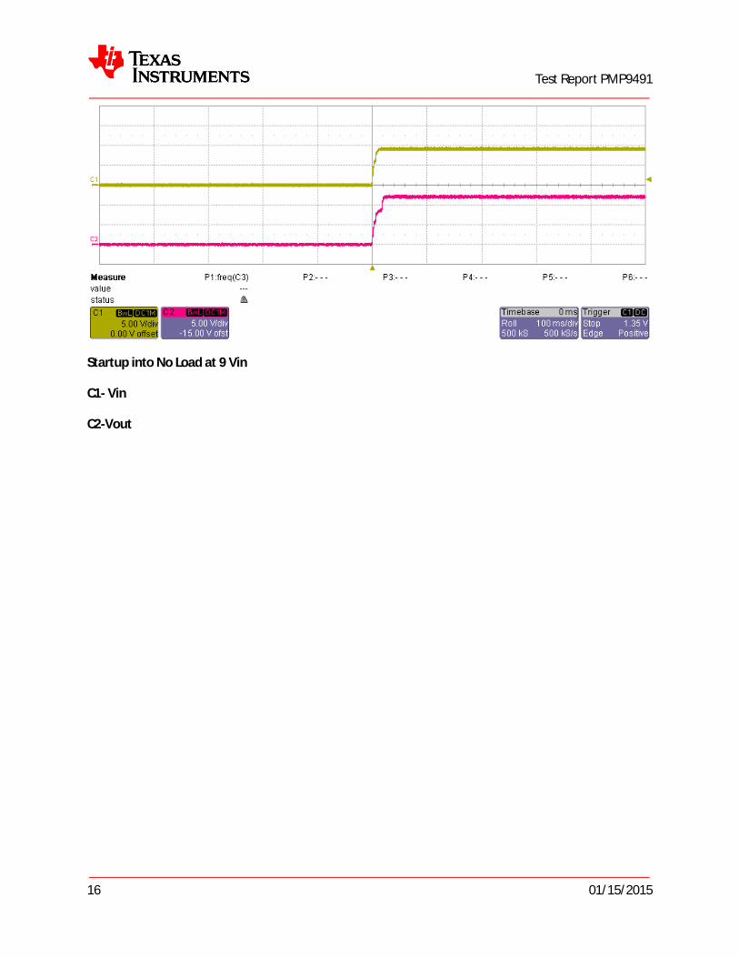
Startup into No Load at 9 Vin
C1- Vin
C2-Vout

Test Report PMP9491
17 01/15/2015
Startup into Load(2.5A) at 9 Vin
C1- Vin
C2-Vout

Test Report PMP9491
18 01/15/2015
4.3.3 Output Voltage Ripple and Switch Node Voltage
C1 - Switch Node Voltage and Ch3-Output Voltage Ripple at 3.5Vin and 2.5A Load
Test Report PMP9491
19 01/15/2015
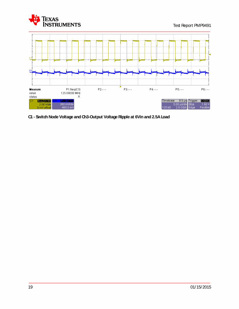
C1 - Switch Node Voltage and Ch3-Output Voltage Ripple at 6Vin and 2.5A Load

Test Report PMP9491
20 01/15/2015
C1 - Switch Node Voltage and Ch3-Output Voltage Ripple at 9Vin and 2.5A Load
Test Report PMP9491
21 01/15/2015
5. Audio Power Amplifier’s Test Result and Jumper Connections
The entire test on Audio Amplifier was done with 5 V input on DC/DC boost converter (output 12V). The results particularly THD Vs Power reveal that Audio performance remains excellent.
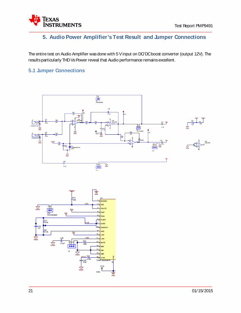
5.1 Jumper Connections
Test Report PMP9491
22 01/15/2015
BTL – Stereo Amplifier Jumpers Position:
Place jumper on J3, remove Jumper on J5, Place Jumper in Position 1-2 on J7, Place Jumper in position
2-3 on J8 and place Jumper in position 2-3 on J12.
PBTL – Woofer Amplifier Jumpers Position:
Remove jumper on J3, place Jumper on J5, Place Jumper in Position 2-3 on J7, Place Jumper in position
1-2 on J8 and place Jumper in position 1-2 on J12.
Connect J9 and J10, Connect J11 and J12 and place 2 Ohm Load across it for testing in PBTL mode
Simple Second order Low Pass Active filters is used in the design for extracting only Low frequency input for Woofer application.

Test Report PMP9491
23 01/15/2015
5.2 BTL: Stereo Waveforms
5.2.1 Input /Output Audio
CH4- Out L+ , CH3- Out L- , CH1-Input L ,Math- CH3-CH4 seen by the 4 Ohm Load
Input -400mV RMS 1 KHz Signal (Gain 26dB)
Test Report PMP9491
24 01/15/2015
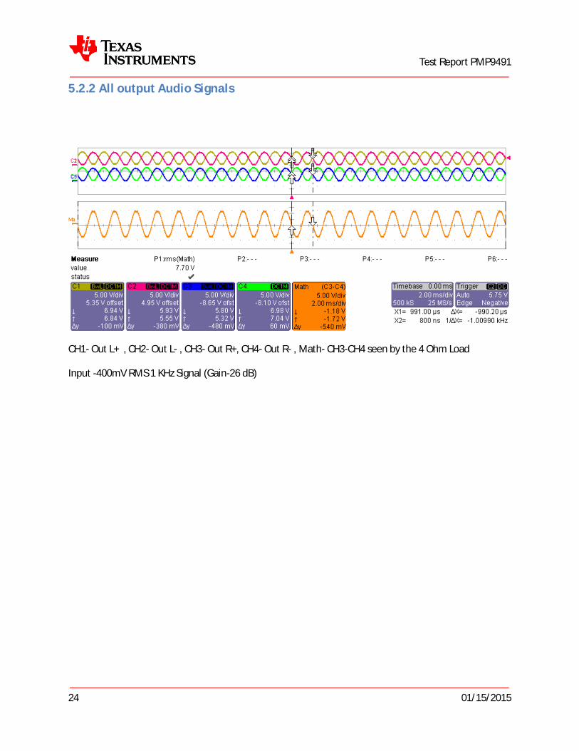
5.2.2 All output Audio Signals
CH1- Out L+ , CH2- Out L- , CH3- Out R+, CH4- Out R- , Math- CH3-CH4 seen by the 4 Ohm Load
Input -400mV RMS 1 KHz Signal (Gain-26 dB)

Test Report PMP9491
25 01/15/2015
5.2.3 THD Vs Power: BTL mode
Test Report PMP9491
26 01/15/2015
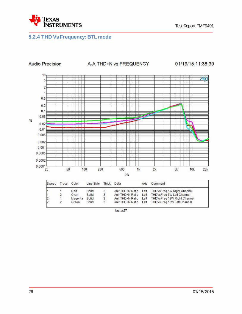
5.2.4 THD Vs Frequency: BTL mode

Test Report PMP9491
27 01/15/2015
5.3 PBTL: Woofer Waveforms
5.3.1 Input /Output Audio Signals
CH1- Out W+(L+ and L- Connected together) , CH2- Out W-(R+ and R- Connected together) , CH3- Input Audio Signal, Math- CH1-CH2 seen by the 2 Ohm Load
Input -300mV RMS 75Hz Signal (26dB gain)

Test Report PMP9491
28 01/15/2015
CH1- Out W+(L+ and L- Connected together) , CH2- Out W-(R+ and R- Connected together) , CH3- Input Audio Signal, Math- CH1-CH2 seen by the 2 Ohm Load
Input -300mV RMS 100Hz Signal (26dB gain)

Test Report PMP9491
29 01/15/2015
CH1- Out W+(L+ and L- Connected together) , CH2- Out W-(R+ and R- Connected together) , CH3- Input Audio Signal, Math- CH1-CH2 seen by the 2 Ohm Load
Input -300mV RMS 150Hz Signal (26dB gain)
Test Report PMP9491
30 01/15/2015
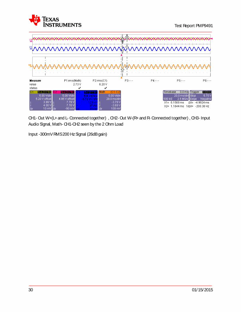
CH1- Out W+(L+ and L- Connected together) , CH2- Out W-(R+ and R- Connected together) , CH3- Input Audio Signal, Math- CH1-CH2 seen by the 2 Ohm Load
Input -300mV RMS 200 Hz Signal (26dB gain)

Test Report PMP9491
31 01/15/2015
CH1- Out W+(L+ and L- Connected together) , CH2- Out W-(R+ and R- Connected together) , CH3- Input Audio Signal, Math- CH1-CH2 seen by the 2 Ohm Load
Input -300mV RMS 2000 Hz Signal (out of Woofer Range)
Test Report PMP9491
32 01/15/2015
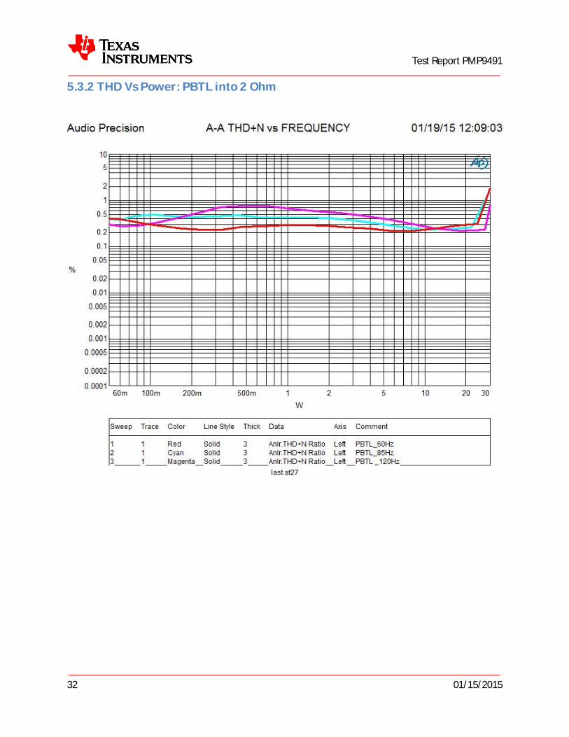
5.3.2 THD Vs Power: PBTL into 2 Ohm
Test Report PMP9491
33 01/15/2015
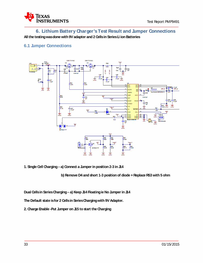
6. Lithium Battery Charger’s Test Result and Jumper Connections All the testing was done with 9V adapter and 2 Cells in Series Li ion Batteries
6.1 Jumper Connections
1. Single Cell Charging – a) Connect a Jumper in position 2-3 in J14
b) Remove D4 and short 1-3 position of diode + Replace R53 with 5 ohm
Dual Cells in Series Charging – a) Keep J14 Floating ie No Jumper in J14
The Default state is for 2 Cells in Series Charging with 9V Adapter.
2. Charge Enable -Put Jumper on J15 to start the Charging

Test Report PMP9491
34 01/15/2015
6.2 Charging Current and Switch Waveform
C4- Charging Current
C1- Switch Waveform of BQ24133 Battery Charger
Test Report PMP9491
35 01/15/2015
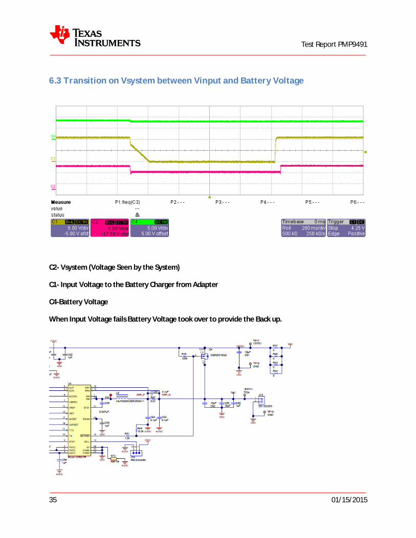
6.3 Transition on Vsystem between Vinput and Battery Voltage
C2- Vsystem (Voltage Seen by the System)
C1- Input Voltage to the Battery Charger from Adapter
C4-Battery Voltage
When Input Voltage fails Battery Voltage took over to provide the Back up.

IMPORTANT NOTICE FOR TI REFERENCE DESIGNS
Texas Instruments Incorporated ("TI") reference designs are solely intended to assist designers (“Buyers”) who are developing systems thatincorporate TI semiconductor products (also referred to herein as “components”). Buyer understands and agrees that Buyer remainsresponsible for using its independent analysis, evaluation and judgment in designing Buyer’s systems and products.TI reference designs have been created using standard laboratory conditions and engineering practices. TI has not conducted anytesting other than that specifically described in the published documentation for a particular reference design. TI may makecorrections, enhancements, improvements and other changes to its reference designs.Buyers are authorized to use TI reference designs with the TI component(s) identified in each particular reference design and to modify thereference design in the development of their end products. HOWEVER, NO OTHER LICENSE, EXPRESS OR IMPLIED, BY ESTOPPELOR OTHERWISE TO ANY OTHER TI INTELLECTUAL PROPERTY RIGHT, AND NO LICENSE TO ANY THIRD PARTY TECHNOLOGYOR INTELLECTUAL PROPERTY RIGHT, IS GRANTED HEREIN, including but not limited to any patent right, copyright, mask work right,or other intellectual property right relating to any combination, machine, or process in which TI components or services are used.Information published by TI regarding third-party products or services does not constitute a license to use such products or services, or awarranty or endorsement thereof. Use of such information may require a license from a third party under the patents or other intellectualproperty of the third party, or a license from TI under the patents or other intellectual property of TI.TI REFERENCE DESIGNS ARE PROVIDED "AS IS". TI MAKES NO WARRANTIES OR REPRESENTATIONS WITH REGARD TO THEREFERENCE DESIGNS OR USE OF THE REFERENCE DESIGNS, EXPRESS, IMPLIED OR STATUTORY, INCLUDING ACCURACY ORCOMPLETENESS. TI DISCLAIMS ANY WARRANTY OF TITLE AND ANY IMPLIED WARRANTIES OF MERCHANTABILITY, FITNESSFOR A PARTICULAR PURPOSE, QUIET ENJOYMENT, QUIET POSSESSION, AND NON-INFRINGEMENT OF ANY THIRD PARTYINTELLECTUAL PROPERTY RIGHTS WITH REGARD TO TI REFERENCE DESIGNS OR USE THEREOF. TI SHALL NOT BE LIABLEFOR AND SHALL NOT DEFEND OR INDEMNIFY BUYERS AGAINST ANY THIRD PARTY INFRINGEMENT CLAIM THAT RELATES TOOR IS BASED ON A COMBINATION OF COMPONENTS PROVIDED IN A TI REFERENCE DESIGN. IN NO EVENT SHALL TI BELIABLE FOR ANY ACTUAL, SPECIAL, INCIDENTAL, CONSEQUENTIAL OR INDIRECT DAMAGES, HOWEVER CAUSED, ON ANYTHEORY OF LIABILITY AND WHETHER OR NOT TI HAS BEEN ADVISED OF THE POSSIBILITY OF SUCH DAMAGES, ARISING INANY WAY OUT OF TI REFERENCE DESIGNS OR BUYER’S USE OF TI REFERENCE DESIGNS.TI reserves the right to make corrections, enhancements, improvements and other changes to its semiconductor products and services perJESD46, latest issue, and to discontinue any product or service per JESD48, latest issue. Buyers should obtain the latest relevantinformation before placing orders and should verify that such information is current and complete. All semiconductor products are soldsubject to TI’s terms and conditions of sale supplied at the time of order acknowledgment.TI warrants performance of its components to the specifications applicable at the time of sale, in accordance with the warranty in TI’s termsand conditions of sale of semiconductor products. Testing and other quality control techniques for TI components are used to the extent TIdeems necessary to support this warranty. Except where mandated by applicable law, testing of all parameters of each component is notnecessarily performed.TI assumes no liability for applications assistance or the design of Buyers’ products. Buyers are responsible for their products andapplications using TI components. To minimize the risks associated with Buyers’ products and applications, Buyers should provideadequate design and operating safeguards.Reproduction of significant portions of TI information in TI data books, data sheets or reference designs is permissible only if reproduction iswithout alteration and is accompanied by all associated warranties, conditions, limitations, and notices. TI is not responsible or liable forsuch altered documentation. Information of third parties may be subject to additional restrictions.Buyer acknowledges and agrees that it is solely responsible for compliance with all legal, regulatory and safety-related requirementsconcerning its products, and any use of TI components in its applications, notwithstanding any applications-related information or supportthat may be provided by TI. Buyer represents and agrees that it has all the necessary expertise to create and implement safeguards thatanticipate dangerous failures, monitor failures and their consequences, lessen the likelihood of dangerous failures and take appropriateremedial actions. Buyer will fully indemnify TI and its representatives against any damages arising out of the use of any TI components inBuyer’s safety-critical applications.In some cases, TI components may be promoted specifically to facilitate safety-related applications. With such components, TI’s goal is tohelp enable customers to design and create their own end-product solutions that meet applicable functional safety standards andrequirements. Nonetheless, such components are subject to these terms.No TI components are authorized for use in FDA Class III (or similar life-critical medical equipment) unless authorized officers of the partieshave executed an agreement specifically governing such use.Only those TI components that TI has specifically designated as military grade or “enhanced plastic” are designed and intended for use inmilitary/aerospace applications or environments. Buyer acknowledges and agrees that any military or aerospace use of TI components thathave not been so designated is solely at Buyer's risk, and Buyer is solely responsible for compliance with all legal and regulatoryrequirements in connection with such use.TI has specifically designated certain components as meeting ISO/TS16949 requirements, mainly for automotive use. In any case of use ofnon-designated products, TI will not be responsible for any failure to meet ISO/TS16949.IMPORTANT NOTICE
Mailing Address: Texas Instruments, Post Office Box 655303, Dallas, Texas 75265Copyright © 2015, Texas Instruments Incorporated


![1.6L 4-CYL - VIN [A] & 1.8L 4-CYL - VIN [A]](https://img.pdfslide.us/doc/110x75/61789fad5dd459523072558c/16l-4-cyl-vin-a-amp-18l-4-cyl-vin-a.jpg)