Embed Size (px)
Citation preview

Test and Fault-Tolerance for Network-on-Chip Infrastructures
by
Cristian Grecu
B.Sc., Technical University of Iasi, 1996
M.A.Sc., The University of British Columbia, 2003
A THESIS SUBMITTED IN PARTIAL FULFILLMENT OF THE REQUIREMENT FOR THE DEGREE OF
DOCTOR OF PHILOSOPHY
in
The Faculty of Graduate Studies
(Electrical and Computer Engineering)
THE UNIVERSITY OF BRITISH COLUMBIA(Vancouver)
© Cristian Grecu, 2008
November 2008
ii
Abstract
The demands of future computing, as well as the challenges of nanometer-era VLSIdesign, will require new design techniques and design styles that are simultaneouslyhigh-performance, energy-efficient, and robust to noise and process variation. One of theemerging problems concerns the communication mechanisms between the increasingnumber of blocks, or cores, that can be integrated onto a single chip. The bus-basedsystems and point-to-point interconnection strategies in use today cannot be easily scaledto accommodate the large numbers of cores projected in the near future. Network-on-chip(NoC) interconnect infrastructures are one of the key technologies that will enable theemergence of many-core processors and systems-on-chip with increased computingpower and energy efficiency. This dissertation is focused on testing, yield improvementand fault-tolerance of such NoC infrastructures.
The motivation for the work is that, with technology scaling into the nanometerrange, defect densities will become a serious challenge for fabrication of integratedcircuits counting billions of transistors. Manufacturing these systems in high volumes canonly be possible if their cost is low. The test cost is one of the main components of thetotal chip cost. However, relying on post-manufacturing test alone for guaranteeing thatICs will operate correctly will not suffice, for two reasons: first, the increased fabricationproblems that are expected to characterize upcoming technology nodes will adverselyaffect the manufacturing yield, and second, post-fabrication faults may develop due toelectromigration, thermal effects, and other mechanisms. Therefore, solutions must bedeveloped to tolerate faults of the NoC infrastructure, as well as of the functional cores.
In this dissertation, a fast, efficient test method is developed for NoCs, that exploitstheir inherent parallelism to reduce the test time by transporting test data on multiplepaths and testing multiple NoC components concurrently. The improvement of test timevaries, depending on the NoC architecture and test transport protocol, from 2X to 34X,compared to current NoC test methods. This test mechanism is used subsequently toperform detection of NoC link permanent faults, which are then repaired by an on-chipmechanism that replaces the faulty signal lines with fault-free ones, thereby increasingthe yield, while maintaining the same wire delay characteristics. The solution describedin this dissertation improves significantly the achievable yield of NoC inter-switchchannels – from 4% improvement for an 8-bit wide channel, to a 71% improvement for a128-bit wide channel. The direct benefit is an improved fault-tolerance and increasedyield and long-term reliability of NoC-based multicore systems.

iii
Table of ContentsAbstract ......................................................................................................... iiTable of Contents......................................................................................... iiiList of Tables................................................................................................. vList of Figures .............................................................................................. vi
Acknowledgments........................................................................................ ix1 Introduction ........................................................................................... 1
1.1 Dissertation contribution.................................................................................. 92 Background on Network-on-chip Testing ......................................... 11
2.1 Introduction..................................................................................................... 112.2 Multi-processor systems-on-chip ................................................................... 112.3 Networks-on-chip ............................................................................................ 132.4 Network-on-chip test – previous work.......................................................... 142.5 Fault models for NoC infrastructure test ..................................................... 18
2.5.1 Wire/crosstalk fault models for NoC inter-switch links ......................... 192.5.2 Logic/memory fault models for FIFO buffers in NoC switches ............ 20
2.6 Summary.......................................................................................................... 233 Test Time Minimization for Networks-on-Chip .............................. 24
3.1 Test data organization .................................................................................... 243.2 Testing NoC switches...................................................................................... 253.3 Testing NoC links............................................................................................ 263.4 Test data transport ......................................................................................... 28
3.4.1 Multicast test transport mechanism ........................................................ 303.5 Test scheduling ................................................................................................ 35
3.5.1 Test time cost function ............................................................................. 373.5.2 Test transport time minimization............................................................. 393.5.3 Unicast test scheduling ............................................................................ 413.5.4 Multicast test scheduling ......................................................................... 44
3.6 Experimental results ....................................................................................... 483.6.1 Test output evaluation.............................................................................. 483.6.2 Test modes for NoC components ............................................................. 493.6.3 Test scheduling results............................................................................. 50
3.7 Summary.......................................................................................................... 574 Fault-tolerance Techniques for Networks-on-chip .......................... 59
4.1 Introduction..................................................................................................... 604.2 Traditional fault-tolerance metrics ............................................................... 654.3 Fault-tolerance metrics for network-on-chip subsystems ........................... 674.4 Metrics evaluation........................................................................................... 734.5 Summary.......................................................................................................... 82
5 Fault-tolerant Global Links for Inter-core Communication inNetworks-on-chip ...................................................................................... 83
5.1 Introduction..................................................................................................... 835.2 Related work.................................................................................................... 84
List of Acronyms and Abbreviations .....................................................viii

iv
5.3 Problem statement .......................................................................................... 865.4 Interconnect yield modeling and spare calculation ..................................... 885.5 Fault-tolerant NoC links ................................................................................ 905.6 Sparse crossbar concentrators....................................................................... 915.7 Fault tolerant global interconnects based on balanced crossbars .............. 955.8 Link test and reconfiguration mechanisms ................................................ 103
5.8.1 Testing the sparse crossbar matrix and interconnect wires ................. 1045.8.2 Link reconfiguration.............................................................................. 1075.8.3 Yield, performance and cost analysis .................................................... 110
5.9 Summary........................................................................................................ 1146 Conclusions ........................................................................................ 115
6.1 Summary of contributions ........................................................................... 1156.2 Limitations..................................................................................................... 1166.3 Future work ................................................................................................... 117
7 Appendices ......................................................................................... 1227.1 Appendix 1: Proof of Correctness for Algorithms 1 and 2 ....................... 1227.2 Appendix 2: Algorithm for balancing fault-tolerant sparse crossbars .... 125
References ................................................................................................. 129

v
List of TablesTable 3-1: Unicast test data scheduling for the example in Fig. 3-7........................... 44Table 3-2: Multicast test data scheduling for the example in Fig. 3-7 ....................... 47Table 3-4: Gate count and comparison for the proposed test mechanism ............... 56Table 3-5: Test scheduling run-times ........................................................................... 57Table 4-1: Detection latency (10-10 flit error rate) ....................................................... 81Table 4-2: Recovery latency (10-10 flit error rate) ....................................................... 81Table 5-1: Effective yield improvement vs interconnect complexity ....................... 111Table 5-2: Test and reconfiguration time overhead .................................................. 113

vi
List of FiguresFigure 1-1: a) Regular NoC. b) Irregular NoC. ............................................................. 2Figure 1-2: (a) Global links in NoC-based systems-on-chip; (b) global inter-core link
with m signal lines; (c) interconnect line spanning multiple metal/via levels...... 5Figure 2-1: MP-SoC platform........................................................................................ 12Figure 2-2: Network-on-chip building blocks in a mesh configuration ..................... 14Figure 2-3: Test configurations in [29]: (a) straight paths; (b) turning paths; (c) local
resource connections ............................................................................................... 15Figure 2-4: Core-based test of NoC routers using an IEEE 1500 test wrapper and
scan insertion [30] ................................................................................................... 16Figure 2-5: Test data transport for NoC router testing using (a) multicast and (b)
unicast [26]............................................................................................................... 17Figure 2-6: Examples of faults that can affect NoC infrastructures: (a) crosstalk
faults; (b) memory faults in the input/output buffers of the switches; (c)short/open interconnect faults; (d) stuck-at faults affecting the logic gates ofNoC switches............................................................................................................ 18
Figure 2-7: MAF crosstalk errors (Y2 – victim wire; Y1, Y3 – aggressor wires). ...... 20Figure 2-8: (a) 4-port NoC switch – generic architecture; (b) dual port NoC FIFO.22Figure 3-1: Test packet structure .................................................................................. 25Figure 3-2: a) Wire i and adjacent wires; b) Test sequence for wire i; c) Conceptual
state machine for MAF patterns generation. ....................................................... 27Figure 3-3: (a) Unicast data transport in a NoC; (b) multicast data transport in a
NoC (S – source; D – destination; U – switches in unicast mode; M – switches inmulticast mode). ...................................................................................................... 29
Figure 3-4: 4-port NoC switch with multicast wrapper unit (MWU) for test datatransport. ................................................................................................................. 31
Figure 3-5: Multicast route for test packets. ................................................................ 34Figure 3-6: (a), (b): Unicast test transport. (c) Multicast test transport.................... 37Figure 3-7: 4-switch network with unidirectional links. ............................................. 43Figure 3-8: Test packets processing and output comparison...................................... 49Figure 4-1: Processes communicating across a NoC fabric ........................................ 68Figure 4-2: Hierarchical partitioning for fault tolerant NoC designs........................ 68Figure 4-3: Average detection latency for end-to-end (e2e), switch-to-switch (s2s),
and code-disjoint (cdd) detection schemes............................................................ 74Figure 4-4: Average recovery latency for equal priority recovery (epr) and priority
based recovery (pbr). .............................................................................................. 76Figure 4-5: Average recovery latency for pbr scheme with variable flit error rate . 78Figure 4-6: Average message latency vs. bound on MAP. .......................................... 79Figure 4-7: Processes P1, P2 mapped on a mesh NoC with QoS communication
constraints................................................................................................................ 80Figure 4-8: Performance and cost of detection techniques. ........................................ 80Figure 5-1: (a) Non-fault-tolerant sparse crossbar and crosspoint implementation;
(b) n-m fault-tolerant sparse crossbar. ................................................................. 92Figure 5-2: Fastest and slowest propagation delay paths for non-balanced fault-
tolerant links............................................................................................................ 93

vii
Figure 5-3: Delay variation for imbalanced fault-tolerant links with 25%redundancy. ............................................................................................................. 84
Figure 5-4: Balancing an (n-m) fault-tolerant sparse crossbar through successivecolumn exchange operations; m=5, n=11.............................................................. 98
Figure 5-5: Delay variation for balanced (b) links with 25% redundancy.............. 100Figure 5-6: Delay variation versus degree of redundancy for a 64-bit link ............ 102Figure 5-7: Delay variation versus crossbar size and degree of redundancy. ......... 102Figure 5-8: Self-test and repair link architecture with shared test and
reconfiguration blocks .......................................................................................... 104Figure 5-9: Link-level test and reconfiguration. ........................................................ 105Figure 5-10: Test and reconfiguration hardware. ..................................................... 107Figure 5-11: Link reconfiguration algorithm............................................................. 108Figure 5-12: Physical link width (n) for different values of logic link width (m = 32,
64, 128 bits) and target effective yield (Yeff). ...................................................... 110Figure 5-13: Area overhead for different crossbar sizes and degrees of redundancy.
................................................................................................................................. 112

viii
ATE: Automated Test Equipment
ATPG: Automated Test Pattern Generation
CAD: Computer Aided Design
CMOS: Complementary Metal Oxide Semiconductor
CMP: Chip Multi-Processors
CPU: Central Processing Unit
DFT: Design for Test
DFM: Design for Manufacturability
DRC: Design Rule Checking
DSP: Digital Signal Processor
FIFO: First In First Out
FO4: Fan-out of four
FPGA: Field Programmable Gate Array
IC: Integrated Circuit
IP: Intellectual Property
ISO: International Organization for Standardization
ITRS: International Technology Roadmap for Semiconductors
I/O: Input/Output
MAF: Maximum Aggressor Fault
MAP: Message Arrival Probability
MP-SoC: Multi-processor System-on-chip
MWU: Multicast Wrapper Unit
NMR: N-Modular Redundancy
NoC: Network-on-chip
OSI: Open Systems Interconnection
QoS: Quality of Services
RISC: Reduced Instruction Set Computer
RLB: Routing Logic Block
SoC: System-on-chip
TAM: Test Access Mechanism
TTPE: Test Time per Element
TT: Test Time
VLSI: Very Large Scale Integration
List of Acronyms and Abbreviations

ix
Acknowledgments
I would like to thank my research supervisors, Professors André Ivanov and Resve
Saleh, for their continued support along my graduate studies. Without their guidance and
help, this work would have not been possible.
I would also like to thank my colleague and friend Partha Pande, for his advice,
participation and help in my research.
Special thanks are due to my wife, Gabriela, who supported me unconditionally all
these years.
This work was partially supported by NSERC of Canada and Micronet.

1
Chapter 1
1 Introduction
The microprocessor industry is moving from a single-core processor to multi-core
and, in the foreseeable future, to many-core processor architectures built with tens to
hundreds of identical cores arranged as chip multi-processors (CMPs) [1]. Another
similar trend can be seen in the evolution of systems-on-chip (SoCs) from single-
processor systems with a set of peripherals to heterogeneous multi-core systems,
composed of several different types of processing elements and peripherals (memory
blocks, hardware accelerators, custom designed cores, input/output blocks, etc.) [2].
Microprocessor vendors are also venturing forwards to mixed approaches, combining
multiple identical processors with different types of cores, such as the AMD Fusion
family [3], which combines together multiple identical CPU cores and a graphics
processor in one design.
Such multi-core, multi-processor systems, whether homogeneous, heterogeneous, or
hybrid, must be interconnected in a manner that is high-performance, scalable, and
reliable. The emerging design paradigm that targets such interconnections is called an on-
chip interconnection network, or network-on-chip (NoC). The basic idea of the NoC
paradigm can be summarized as “route packets, not wires” [4]. Interconnecting cores
through an on-chip network has several advantages over dedicated point-to-point or
bus-based wiring, offering potential advantages in terms of high aggregate bandwidth,

2
low communication latency, low power dissipation in inter-core communication, and
increased scalability, modularity and flexibility.
The potential of NoCs is, however, far from being fully realized, and their practical
implementation presents numerous challenges [5]. The first set of challenges is associated
with meeting power/performance targets. The second set of issues relates to CAD tools
and design methodologies to cope with the typical number of devices (in the range of one
billion transistors or more), and the high degree of hardware and software parallelism that
is characteristic of NoC-based systems.
Network-on-chip architectures were proposed as a holistic solution for a set of
challenges faced by designers of large, multi-core systems-on-chip. In general, two types
of NoC architectures can be identified, as shown in Fig. 1-1: (a) regular interconnection
structures derived from parallel computing, and (b) irregular, custom-built NoC fabrics.
The infrastructure for NoC includes switches, inter-switch wires, interface blocks to
connect to the cores, and a protocol for data transmission [6]. There is a significant
number of active research efforts to bring NoCs into mainstream use [7].
(a) (b)
- Functional core
- Switch
Figure 1-1: a) Regular NoC. b) Irregular NoC.

3
The power dissipation of current NoC implementations is estimated to be
significantly higher (in the order of 10 times or more) compared to the expected power
budget of future CMP interconnects [5]. Both circuit-level and architecture-level
techniques must be combined in order to reduce the power dissipation of NoC-based
systems and their data-communication sub-systems to acceptable values.
The data transport latency of NoC infrastructures is too large for the current
programming models, leading to significant performance degradation, especially in the
case of on-chip memory access operations. Here, various research efforts are focused on
reduced-latency router microarchitecture design [8], circuit techniques that reduce signal
propagation time through NoC channels [9], and network architectures with reduced
number of hops for latency-critical data transfers [10].
From a CAD perspective, most of the NoC architectures and circuit techniques are
incompatible with the current design flows and tools, making them difficult to integrate
in the typical SoC design flow. The fundamental reason is the high degree of parallelism
at both computation and data transport levels, combined with the different ways in which
the software and hardware components of a NoC interact with each other.
A major challenge that SoC designers are expected to face [11] is related to the
intrinsic unreliability of the communication infrastructure due to technology limitations.
Two different sources can be identified: random and systematic. The random defects
arise from the contaminants, particles and scratches [12] that occur during the fabrication
process. The systematic defects have roots in the photolithographic process, chemical-
mechanical polishing methods and the continuous feature size shrinking in semiconductor
fabrication technology. Chips are increasingly prone to feature corruption producing

4
shorts and opens in the wires, and missing vias, or vias with voids, as a result of
photolithographic limitations. In addition, the effect of steps such as chemical-mechanical
polishing may cause surface dishing through over-polishing, ultimately becoming
important yield-loss factors [13].
Metal and via layers in advanced CMOS processes are characterized by defect
densities correlated with their specific physical dimensions. Upper layers of metal tend to
be wider and taller due to the expected current levels. The fabrication of wider wires does
not present as much of a problem to photolithographic techniques; however, the vias tend
to be tall and thin and are prone to voids. Therefore, via duplication or via arrays are
employed to circumvent this issue.
Producing fine-lined wires presents the greatest challenge to the resolution of the
most advanced photolithographic capabilities available today. Mitigating all these general
observations is the fact that, in a typical foundry, older generations of equipment are used
to fabricate the middle and upper layers of metal, each with their own yield
characteristics. It is expected that the overall yield of interconnects will continue to
decrease as the number of metal layers increases (e.g., 12 metal layers for 45 nm
technology, compared with 9 layers for a typical 90nm process, and 5 layers for a 180nm
process), as projected by the ITRS documents [14].
The impact on the overall yield of multi-core chips [15] can be quite significant,
given that the data communication infrastructure alone can consume around 10-15% of
the total chip area [16]. The inter-core communication links are likely to be routed on the
middle and upper metal layers. Hence, the layout scenario is very similar to the example
shown in Fig. 1-2, which illustrates a multi-processor SoC built on a network-on-chip

5
platform, consisting of functional cores, switching blocks and global links. The active
devices (processing cores, memory blocks) are on the lower levels on the silicon surface,
and the inter-core wires are on the higher levels of the 3D structure [17]. Global signal
lines span more metal layers and require more levels of vias in order to go to/from the
active devices on the silicon surface and therefore are more prone to manufacturing
defects.
Figure 1-2: (a) Global links in NoC-based systems-on-chip; (b) global inter-core link with msignal lines; (c) interconnect line spanning multiple metal/via levels.
Many authors have tried to make the case for the network-on-chip paradigm by
stating that “wires are free” and consequently an interconnect architecture consisting of
many multi-wire links is, by default, feasible and efficient. In fact, wires are expensive in
terms of the cost of the masks that are required in the successive steps of the fabrication
of interconnect metal layers through photolithography. Moreover, they are not free in
terms of the possible defects that can appear due to technology constraints specific to an

6
increase in the number of metal layers for every process generation, and continuous
increase in the aspect ratio of wires (the ratio between their vertical and horizontal
dimensions). While the wires on the lower layers can be made with an aspect ratio of less
than one, the interconnects on middle and upper metal layers require an aspect ratio of
two or higher. This, in turn, places an increased difficulty in achieving reliable contact
between wires on different layers, since the vias between such wires will need to be
relatively tall and narrow, and as a consequence more likely to exhibit open or resistive
defects.
Currently, via duplication is the solution that attempts to address this issue by
inserting redundant vias in the routing stage of the chip layout design phase. This method
for improving interconnect yield is ad-hoc in nature and can only provide results if
enough space is left on the upper level metal layers to insert the redundant vias while
preserving the design rules. Most of the authors of technical articles on the topic of via
duplication state clearly that, ideally, the solution for interconnect yield improvement
should be pushed earlier in the design flow of ICs, more preferably in the front-end rather
than in the back-end. A universal front-end solution for improving interconnect yield has
not yet been found. However, by examining the categories of interconnect that are more
prone to defects, it is possible to develop custom solutions targeting particular
interconnect types.
That is, in order to ensure correct fabrication, faults must be detected through post-
fabrication testing, and, possibly, compensated for through fault-tolerant techniques.
When looking in particular at design, test, manufacturing and the associated CAD
tools in the NoC design flow in the context of shrinking transistor size and wire

7
dimensions, it is clear that fabrication defects and variability are significant challenges
that are often overlooked. On-chip networks need mechanisms to ensure correct
fabrication and life-time operation in presence of new defect/fault mechanisms, process
variability, and high availability requirements.
Traditionally, correct fabrication of integrated circuits is verified by post-
manufacturing testing using different techniques ranging from scan-based techniques to
delay test and current-based test. Due to their particular nature, NoCs are exposed to a
wide range of faults that can escape the classic test procedures. Among such faults we
can enumerate crosstalk, faults in the buffers of the NoC routers, and higher-level faults
such as packet misrouting and data scrambling [6]. These fault types add to the classic
faults that must be tested after fabrication for all integrated circuits (stuck-at, opens,
shorts, memory faults, etc.). Consequently, the test time of NoC-based systems increases
considerably due to these new faults.
Test time is an important component of the test cost and, implicitly, of the total
fabrication cost of a chip. For large volume production, the total chip testing time must be
reduced as much as possible in order to keep the total cost low. The total test time of an
IC is governed by the amount of test data that must be applied and the amount of
controllability/observability that the design-for-test (DFT) strategy chosen by designers
can provide. The test data increases with chip complexity and size, so the option the DFT
engineers are left with is to improve the controllability/observability. Traditionally, this is
achieved by increasing the number of test inputs/outputs, but this has the same effect of
increasing the total cost of the IC.

8
DFT techniques such as scan-based test improve the controllability and observability
of IC internal components by serializing the test input/output data and feeding/extracting
it to/from the IC through a reduced number of test pins. The trade-off is the increase in
test time and test frequency, which makes at-speed test difficult using scan-based
techniques. While scan-based solutions are useful, their limitations in the particular case
of NoC systems demand the development of new test data generation and transport
mechanisms that simultaneously minimize the total test time and the number of test I/O
pins.
In this work, two types of solutions are proposed to reduce the test time of NoC data
transport infrastructures: first, we use a built-in self-test solution to generate test data
internally, eliminating the need to inject test data using I/O pins. Second, we replace the
use of a traditional dedicated test access mechanism (TAM) with a test transport
mechanism that reuses the NoC infrastructure progressively to transport test data to NoC
components under test. This approach has the advantage that it exploits the inherent high
degree of parallelism of the NoC, thus allowing the delivery of multiple test vectors in
parallel to multiple NoC components under test. A multicast test delivery mechanism is
described, with one test data source that sends test data in a parallel fashion along the
subset of already tested NoC components. The test data routing algorithm is optimized
off-line, deterministically, such that the shortest paths are always selected for forwarding
test packets. This techniques guarantees that the test transport time is minimized which,
together with the advantage of testing multiple NoC components in parallel, yields a
reduced test time for the overall NoC.

9
An effective and efficient test procedure is necessary, but not sufficient to guarantee
the correct operation of NoC data transport infrastructures during the life-time of the
integrated circuits. Defects may appear later in the field, due to causes such as
electromigration, thermal effects, material ageing, etc. These effects will become more
pronounced with continuous downscaling of device dimensions beyond 65 nm and
moving towards the nanoscale domain. New methods are needed to enhance the yield of
these links to make them more reliable. The fault-tolerant solution using reconfigurable
crossbars and redundant links developed in this work is aimed specifically at the NoC
links, and allows both post-fabrication yield tuning and self-repair of links that may break
down later in the life-cycle of the chip.
1.1 Dissertation contribution
This dissertation offers three major contributions:
1. A complete NoC test methodology, including the hardware circuitry and
scheduling algorithms, which together minimize the test time by
distributing test data concurrently to multiple components of the NoC
fabric.
2. An evaluation of various fault-tolerance mechanisms for NoC
infrastructures, and two new metrics relevant to quality-of-services on
NoCs.
3. A fault-tolerant design method for NoC links that allows fine yield tuning
and life-cycle self-repair of NoC interconnect infrastructures. This method
uses the above-mentioned test mechanism to diagnose and identify the
faulty interconnects.

10
The rest of this dissertation is organized as follows: Chapter 2 presents background
on network-on-chip test aspects and fault models. Chapter 3 presents contribution (1) - a
test methodology and scheduling algorithms that minimize the test time of NoC of
arbitrary topologies. Chapter 4 presents contribution (2) - an overview and evaluation of
fault-tolerance mechanisms and two proposed metrics relevant to NoCs. Chapter 5
describes contribution (3) - a method to provide design fault-tolerant NoC links based on
sparse crossbars and tune the yield of NoC links based on the expected defect rate.
Chapter 6 concludes the dissertation, outlines a few limitations of the proposed
approaches, and provides a set of possible future research directions that can be pursued
as a direct follow-up to the contributions presented in this dissertation.

11
Chapter 2
2 Background on Network-on-chip Testing
2.1 Introduction
System-on-Chip (SoC) design methodologies are currently undergoing revolutionary
changes, driven by the emergence of multi-core platforms supporting large sets of
embedded processing cores. These platforms may contain a set of heterogeneous
components with irregular block sizes and/or homogeneous components with a regular
block sizes. The resulting platforms are collectively referred to as multi-processor SoC
(MP-SoC) designs [7]. Such MP-SoCs imply the seamless integration of numerous
Intellectual Property (IP) blocks performing different functions and exchanging data
through a dedicated on-chip communication infrastructure. A key requirement of these
platforms, whether irregular or regular, is a structured interconnect architecture. The
network-on-chip (NoC) architecture is a leading candidate for this purpose [18].
2.2 Multi-processor systems-on-chip
Since today’s VLSI chips can accommodate in excess of 1 billion transistors, enough to
theoretically place thousands of 32-bit RISC [18] processors on a die, leveraging such
capabilities is a major challenge. Traditionally, SoC design was based on the use of a
slowly evolving set of hardware and software components: general-purpose processors,
digital signal processors (DSPs), memory blocks, and other custom-designed hardware IP
blocks (digital and analog). With a significant increase in the number of components in
complex SoCs, significantly different design methods are required to cope with the deep
sub-micron physical design issues, verification and design-for-test of the resulting SoCs.
12
One of the solutions that the design community adopted to reduce the design cycle is the
platform-based design paradigm, characterized by the use of higher-level off-the-shelf IP
blocks, connected via a modular, scalable SoC interconnect fabric and standard
communication interfaces and protocols. Such MP-SoC platforms are highly flexible,
programmable and/or reconfigurable for application areas such as wireless, multimedia,
networking, automotive. A high-level view of the general MP-SoC platform is given in
Fig. 2-1. When designing with such platforms, no IP design is performed, but
specification, configuration and assembly of existing IP blocks is greatly facilitated.
Figure 2-1: MP-SoC platform [7]
MP-SoC platforms will include, in the near future, tens to hundreds of embedded
processors, in a wide variety of forms, from general-purpose reduced instruction-set
computers (RISC) to application-specific instruction-set processors (ASIP) with different
trade-offs in time-to-market, performance, power and cost. New designs are being
reported from industry [19], with more than 100 embedded heterogeneous processors, for
applications ranging from communications, network processing, to security processors,
storage array networks, and consumer image processing.

13
2.3 Networks-on-chip
A key component of the MP-SoC platform of Fig. 2-1 is the interconnect fabric
connecting the major blocks. Such a fabric must provide orthogonality, scalability,
predictable physical parameters and a plug-and-play design style for integrating various
hard-wired, reconfigurable or programmable IPs. Such architectures must support high-
level, layered communication abstraction, and simplify the automatic mapping of
processing resources onto the interconnect fabric. Networks-on-chip are particularly
suitable for accomplishing these features.
A NoC interconnect fabric is a combination of hardware (switches and inter-switch
links) and software components (communication and interfacing protocols). NoCs can be
organized in various topologies [20] – mesh, tree, ring, irregular, etc…– and can
implement various subsets of the ISO/OSI communication stack [21]. A well-known 2D
mesh NoC topology is illustrated in Fig. 2-2. The term Network-on-chip is used today
mostly in a very broad sense, encompassing the hardware communication infrastructure,
the communication protocols and interfaces, operating system communication services,
and the design methodology and tools for NoC syndissertation and application mapping.
All these components together can be called a NoC platform [7]. Some authors use the
Network-on-chip to denote the entire MP-SoC built on a structured, networked fabric –
including the IP cores, the on-chip communication medium, application software and
communication protocols [20]. In this dissertation, the Network-on-chip term refers to the
on-chip communication architecture, including the hardware components (switches,
links) and communication protocols.

14
Figure 2-2: Network-on-chip building blocks in a mesh configuration
2.4 Network-on-chip test – previous work
While much work has centered on design issues, much less effort has been directed to
testing such NoCs. Any new design methodology will only be widely adopted if it is
complemented by efficient test mechanisms. In the case of NoC-based chips, two main
aspects have to be addressed with respect to their test procedures: how to test the NoC
communication fabric, and how to test the functional cores (processing, memory and
other modules). Since the inception of SoC designs, the research community has targeted
principally the testing of the IP cores [22], giving little emphasis to the testing of their
communication infrastructures. The main concern for SoC test was the design of efficient
test access mechanisms (TAM) for delivering the test data to the individual cores under
constraints such as test time, test power, and temperature. Among the different test access
mechanisms, TestRail [23] was one of the first to address core-based test of SoCs.
Recently, a number of different research groups suggested the reuse of the
communication infrastructure as a test access mechanism [24] [25] [26]. In [27] the
authors assumed the NoC fabric as fault-free and subsequently used it to transport test
data to the functional blocks; however, for large systems, this assumption can be
unrealistic, considering the complexity of the design and communication protocols. In

15
[28], the authors proposed a dedicated TAM based on an on-chip network, where
network-oriented mechanisms were used to deliver test data to the functional cores of the
SoC.
A test procedure for the links of NoC fabrics is presented in [29], targeted specifically
to mesh topologies. The NoC switches are assumed to be tested using conventional
methods first, and then three test configurations are applied in series to diagnose potential
faults of the inter-switch links, as indicated in Fig. 2-3.
(a) (b) (c)
Figure 2-3: Test configurations in [29]: (a) straight paths; (b) turning paths; (c) localresource connections
A configuration is set up by adjusting the corresponding destination address fields of
the transmitted packets to the last row (column) of the network matrix. The three
configurations cover all possible link directions in a mesh NoC: vertical, horizontal,
turning paths, and local connections to processing resources. The major limitations of this
approach are: 1) applicability to mesh-based NoC only; 2) a test procedure for NoC
switches is not defined.
A different approach is presented in [30], based on an extension of the classic
wrapper-based SoC test [23] and scan-chain method [31]. Each NoC switch (or router) is
subjected to scan-chain insertion, and the set of all NoC switches is wrapped with an
16
IEEE 1500 test wrapper and tested using the core-based test approach [23]. The overall
test architecture is presented in Figure 2-4.
test inputs output comparison
Figure 2-4: Core-based test of NoC routers using an IEEE 1500 test wrapper and scaninsertion [30]
The solution presented in [30] addresses the test of the NoC switches only,
overlooking completely the aspect of testing the NoC links. For large NoCs, the method
inherits the limitations of scan-based test when applied to large cores: slow test speed for
long scan chains, the trade-off between the number of test I/Os and scan chain length.
The idea of reusing the NoC fabric for delivering test data to the processing elements
appears also in [26], combined with progressive test of NoC routers and overlapping the
test of routers and processing elements in time to reduce the total test time. Both unicast
and multicast test transport methods are considered, as shown in Figure 2-5.

17
(a) (b)Figure 2-5: Test data transport for NoC router testing using (a) multicast and (b) unicast
[26]
The work presented in [26] does not consider the test of NoC links, and does not
show how to minimize the test transport time in either the unicast or multicast transport
modes. It is also not clear if the proposed solution delivers an optimal test time when
combining test of NoC routers and processing cores.
This dissertation is focused on the test of the NoC infrastructure that includes both
NoC switches and inter-switch links. The work complements previous approaches by
developing the test strategy for the interconnect infrastructure itself. The test strategies of
NoC-based interconnect infrastructures must address two problems [16]: (i) testing of the
switch blocks; (ii) testing of the inter-switch wire segments. The test procedures of both
switches and inter-switch links are integrated in a streamlined fashion. Two novel
techniques characterize the proposed solution. The first is the reuse of the already tested
NoC components to transport the test data towards the components under test in a
recursive manner. The second is employing the inherent parallelism of the NoC structures
to propagate the test data simultaneously to multiple NoC elements under test. Two test
scheduling algorithms are provided that guarantee a minimal test time for arbitrary NoC
topologies. In the next section we elaborate the set of fault models used for designing the
proposed test method, including scheduling algorithms and on-chip test-related hardware.

18
2.5 Fault models for NoC infrastructure test
When developing a test methodology for NoC fabrics, one needs to start from a set of
models that can realistically represent the faults specific to the nature of NoC as a data
transport mechanism. As stated previously, a NoC infrastructure is built from two basic
types of components: switches and inter-switch links. For each type of component, test
patterns must be constructed that exercise its characteristic faults.
- Functional core
- Switch
- Link
‘1’
‘0’
(a)
(b)
(d)
(c)
Figure 2-6: Examples of faults that can affect NoC infrastructures: (a) crosstalk faults; (b)memory faults in the input/output buffers of the switches; (c) short/open interconnect faults;
(d) stuck-at faults affecting the logic gates of NoC switches.
The range of faults that can affect the NoC infrastructure is significant and it extends
from interconnects faults to logic and memory faults. Consequently, the data set required
to test all these faults is extremely large, and carries a major overhead to the overall test
time of NoC-based integrated circuits. A subset of these faults is represented in Fig. 2-6.
In the following subsections the set of faults considered in this work for the NoC
switches and links is presented.

19
2.5.1 Wire/crosstalk fault models for NoC inter-switch links
Cuviello et al. [32] proposed a novel fault model for the global interconnects of DSM
SoCs that accounts for cross-talk effects between a set of aggressor lines and a victim line.
This fault model is referred to as Maximum Aggressor Fault (MAF) and it occurs when
the signal transition on a single interconnect line (called the victim line) is affected
through cross-talk by transitions on all the other interconnect lines (called the aggressors)
due to the presence of the crosstalk effect. In this model, all the aggressor lines switch in
the same direction simultaneously.
The MAF model is an abstract representation of the set of all defects that can lead to
one of the six crosstalk errors: rising/falling delay, positive/negative glitch, and
rising/falling speed-up. The possible errors corresponding to the MAF fault model are
presented in Fig. 2-7 for a link consisting of 3 wires. The signals on lines Y1 and Y3 act
as aggressors, while Y2 is the victim line. The aggressors act collectively to produce a
delay, glitch or speed-up on the victim.
This abstraction covers a wide range of defects including design errors, design rules
violations, process variations and physical defects. For a link consisting of N wires, the
MAF model assumes the worst-case situation with one victim line and (N-1) aggressors.
For links consisting of a large number of wires, considering all such variations is
prohibitive from a test coverage point of view [31].
The transitions needed to sensitize the MAF faults can be easily derived from Fig. 2-7
based on the waveform transitions indicated. For an inter-switch link consisting of N
wires, a total of 6N faults need to be tested, and requiring 6N 2-vector tests. These 6N
MAF faults cover all the possible process variations and physical defects that can cause

20
any crosstalk effect on any of the N interconnects. They also cover more traditional faults
such as stuck-at, stuck-open and bridging faults.
(c)
fault-free signalsignal affected by MAFY , Y : aggressor lines1 3 Y : victim line2
Y1
Y2
Y3
“0”
(a)
gp(positive
glitch)
Y1
Y2
Y3
“1”
(b)
gn(negative
glitch)
Y1
Y2
Y3
(d)
df(delayed
fall)
Y1
Y2
Y3
dr(delayed
rise)
Y1
Y2
Y3
(e)
sr(speedy
rise)
Y1
Y2
Y3
(f)
sf(speedy
fall)
Figure 2-7: MAF crosstalk errors (Y2 – victim wire; Y1, Y3 – aggressor wires).
2.5.2 Logic/memory fault models for FIFO buffers in NoC switches
NoC switches generally consist of a combinational block in charge of functions such
as arbitration, routing, error control, and first-in/first-out (FIFO) memory blocks that
serve as communication buffers [33][34]. Fig. 2-8(a) shows the generic architecture of a

21
NoC switch. As information arrives at each of the ports, it is stored in FIFO buffers and
then routed to the target destination by the routing logic block (RLB).
The FIFO communication buffers for NoC fabrics can be implemented as register
banks [35] or dedicated SRAM arrays [36]. In both cases, functional test is preferable due
to its reduced time duration, good coverage, and simplicity.
The block diagram of a NoC FIFO is shown in Fig. 2-8(b). From a test point of view,
the NoC-specific FIFOs fall under the category of restricted two-port memories. Due to
the unidirectional nature of the NoC communication links, they have one write-only port
and one read-only port, and are referred to as (wo-ro)2P memories. Under these
restrictions, the FIFO function can be divided in three ways: the memory-cells array, the
addressing mechanism, and the FIFO-specific functionality [37].

22
RLB(
)routing logic
blockFIFO FIFO
(a)WRITE PORT
READ PORT
FFWO
EFRO
WCK RCK
WD0
WD1
WDn-1
RD0
RD1
RDn-1
B
(b)
Figure 2-8: (a) 4-port NoC switch – generic architecture; (b) dual port NoC FIFO.
Memory array faults can be stuck-at, transition, data retention or bridging faults [31].
Addressing faults on the RD/WD lines are also important as they may prevent cells from
being read/written. In addition, functionality faults on the empty and full flags (EF and FF,
respectively) are included in our fault models set [37].

23
2.6 Summary
In this chapter, the problems of NoC testing and prior work in this area were
described. Then, the set of fault models that used in this work for developing the test
scheduling algorithms and the associated on-chip test hardware were detailed. Different
fault models are outlined for testing NoC channels and routers. The choice for
constructing test vectors for NoC links is the maximum aggressor fault (MAF) which
takes the worst-case crosstalk scenario into consideration, with the benefit that it also
covers other, more traditional faults (opens, shorts, stuck-at). For the input/output buffers
of the NoC routers we use memory-specific fault models which take into account the
dual-port characteristic of the FIFO buffers and allow functional test for these
components. The routing logic blocks of the NoC switches are simply tested using classic
stuck-at, open, and short fault models.

24
Chapter 3
3 Test Time Minimization for Networks-on-Chip 1
A significant portion of the total production cost of an IC is represented by its
associated test procedures. A direct measure of an IC’s test cost is the time spent for
testing it. With increasing transistor-count and complexity, multi-core SoCs pose a
particular challenge in terms of keeping the test time under reasonable limits. Much
research effort is invested in minimizing the test time of large SoCs, and, consequently,
the total production cost. In the case of NoC-based MP-SoCs, the test time of the NoC
infrastructure adds to the total IC production cost. Reducing the NoC test time contributes
to lowering the total SoC test time, and, implicitly, production cost. This chapter presents
a test method and corresponding hardware circuitry that minimize the test time of NoC
interconnect fabrics.
3.1 Test data organization
A key feature that differentiates a NoC from other on-chip communication media is the
transmission of data in form of packets [4]. In the approach proposed here, the raw test
data, obtained based on the fault models and assumptions outlined in Chapter 2, are
organized into test packets that are subsequently directed towards the different
components of the NoC under test. Test data is organized into packets by adding routing
1 This chapter is based on work published in:1. C. Grecu, P.P. Pande, B. Wang, A. Ivanov, R. Saleh, " Methodologies and algorithms for testing
switch-based NoC interconnects", IEEE Symposium on Defect and Fault Tolerance in VLSISystems, 2005, DFT '05, Oct. 2005.
2. C. Grecu, A. Ivanov, R. Saleh, P.P. Pande, "Testing Networks-on-chip CommunicationInfrastructures", IEEE Transactions on Computer Aided Design, Volume 26, Issue 12, Dec. 2007.

25
and control information to the test patterns generated for each NoC component. The
routing information is similar to that of functional data packets and identifies the
particular NoC component towards which the test packet is directed. The control
information consists of fields that identify the packet type (e.g., test packet) and type of
the NoC component under test (inter-switch link, switch combinational block, FIFO). At
the beginning and the end of each test packet, dedicated fields signal the start and stop
moments of the test sequence, respectively.
T_startT_stop
Test
_con
trol
Figure 3-1: Test packet structure
The test set for the faults presented in Chapter 2 was developed based on [32] and
[37], and includes test vectors for inter-switch links, FIFO buffers, and routing logic
blocks of the NoC switches. The generic structure of a test packet is shown in Fig. 3-1.
The test header field contains routing information and packet identification information
which denotes the type of data being carried (test data). The second field (test control)
contains the type of test data, i.e., interconnect, FIFO, or RLB (routing logic block) test
data. The test data field is bordered by corresponding flags (T_start and T_stop) marking
its boundaries.
3.2 Testing NoC switches
When a test packet arrives at an untested switch, the payload is unpacked to extract the
test data. NoC switches can be tested with standard logic and memory test methods.

26
Scan-based testing [31] is adopted for the routing logic blocks of NoC switches, while
functional test [37] is used for the communication buffers (FIFO memory blocks). Test
patterns are generated for the RLB and FIFO blocks separately so that the test vectors can
be optimized for each type of block. The test of the logic part of the switch (the RLB
block) is performed while it is isolated from the rest of the switch.
Assuming the FIFOs are B bits wide and have n locations, the test uses B-bit patterns.
As an example, consider the detection of a bridging fault, i.e., a short between the bitlines
bi and bj (i ≠ j), that can eventually yield an AND or OR behaviour. In order to detect
such faults, four specific test patterns are used: 0101…, 1010…, 0000…, and 1111…,
denoted by 1G , 1G , 2G , and 2G , respectively [37] . Specifically, to test the dual-port
coupling faults, the following sequence is used:
11nw rw r
for each of the four test patterns above. The first write operation (denoted by w in the
expression above) sets the read/write pointers to FIFO cells 0 and 1, respectively; the
next (n-1) simultaneous read(r)/write(w) operations (denoted by 11n wr ) sensitize the
coupling faults between adjacent cells, and the last read operation (denoted by r) empties
the FIFO and prepares it for the next test pattern. All other standard tests proceed in a
similar manner.
3.3 Testing NoC links
Testing for wire faults and crosstalk effects can be carried out together as follows.
According to the MAF fault model, each possible MAF on a victim line of a link requires
a two-vector test sequence to be sensitized. The test sequence exhibits some useful
properties which allow for a compact and efficient design of the MAF test packets:

27
Property (a): For each test vector, the logic values on the aggressor lines are the
opposite of that on the victim line;
Property (b): After having applied the exhaustive set of test sequences for a
particular victim line, the test sequence of the adjacent victim line can be obtained
by shifting (rotating) the test data by exactly one bit.
If wire i in Fig. 3-2(a) is to be tested for 6 MAF faults, then twelve vectors are
implied, due to the two-vector test needed for each case. However, the transitions from
one test vector to another can be concatenated such that the number of test vectors needed
to sensitize the MAF faults can be reduced from twelve vectors per wire to eight, as
shown in Fig. 3-2(b) and (c).
(a) (b) (c)
Figure 3-2: a) Wire i and adjacent wires; b) Test sequence for wire i; c) Conceptual statemachine for MAF patterns generation.
The test data packets are designed based on Properties (a) and (b) above, by
generating the logical values corresponding to the MAF tests in eight distinct states s1 to
s8. In an s1-to-s8 cycle, the state machine produces eight vectors. During each cycle, one
line is tested and is assigned the victim logic values, while the rest of the lines get the

28
aggressor values. The selection of the victim wire is achieved through the victim line
counter field that controls the test hardware such that for the first eight test cycles, the
first wire of the link is the victim. During the second set of eight test cycles, the second
wire is the victim, and so on. After each eight-vector sequence, the test patterns shift by
one bit position, and an identical eight-vector sequence is applied with a new
corresponding wire acting as the victim. This procedure repeats until all the lines of the
link are completed.
3.4 Test data transport
This section describes the NoC modes of operation and a minimal set of features that
the NoC building blocks must possess for packet-based test data transport. A
system-wide test transport mechanism must satisfy the specific requirements of the NoC
fabric and exploit its highly-parallel and distributed nature for an efficient realization. In
fact, it is advantageous to combine the testing of the NoC inter-switch links with that of
the other NoC components (i.e., the switch blocks) in order to reduce the total silicon area
overhead. The high degree of parallelism of typical NoCs allows simultaneous test of
multiple components. However, special hardware may be required to implement parallel
testing features.
Each NoC switch is assigned a binary address such that the test packets can be directed
to particular switches. In the case of direct-connected networks, this address is identical
to the address of the IP core connected to the respective switch. In the case of indirect
networks (such as BFT [38] and other hierarchical architectures [39]), not all switches are
connected to IP cores, so switches must be assigned specific addresses in order to be

29
targeted by their corresponding test packets. Considering the degree of concurrency of
the packets being transported through the NoC, two cases can be distinguished:
Unicast mode: the packets have a single destination [40]. This is the more common
situation and it is representative for the normal operation of an on-chip communication
fabric, such as processor cores executing read/write operations from/into memory cores,
or micro-engines transferring data in a pipeline [41]. As shown in Fig. 3-3(a), packets
arriving at a switch input port are decoded and directed to a unique output port, according
to the routing information stored in the header of the packet (for simplicity, functional
cores are not shown in Fig. 3-3). Test packets are injected at the source switch (denoted
by S in Fig. 3-3) and transported towards the destination switch (denoted by D) along the
path indicated by the set of switches in the unicast (U) mode.
(a) (b)
Figure 3-3: (a) Unicast data transport in a NoC; (b) multicast data transport in a NoC (S –source; D – destination; U – switches in unicast mode; M – switches in multicast mode).
Multicast mode: the packets have multiple destinations [42]. This mode is useful for the
management and reconfiguration of functional cores of the NoC, when identical packets
carrying setup and/or configuration information must be transported to the processing
elements [43]. Packets with multicast routing information are decoded at the switch input
ports and then replicated identically at the switch outputs indicated by the multicast

30
decoder. The multicast packets can reach their destinations in a more efficient and faster
manner than in the case when repeated unicast is employed to send identical data to
multiple destinations [44]. Fig. 3-3(b) shows a multicast transport instance, where the
data is injected at the switch source (S), replicated and retransmitted by the intermediate
switches in both multicast (M) and unicast (U) modes, and received by multiple
destination switches (D). The multicast mode is especially useful for test data transport
purposes, when identical blocks need to be tested as fast as possible.
3.4.1 Multicast test transport mechanism
One possible way to multicast is simply to unicast multiple times, but this implies a
very high latency. The all-destination encoding is another simple scheme in which all
destination addresses are carried by the header. This encoding scheme has two
advantages. First, the same routing hardware used for unicast messages can be used for
multi-destination messages. Second, the message header can be processed on the fly as
address flits arrive. The main problem with this scheme is that, as the number of switch
blocks in the system increases, the header length increases accordingly and thereby
results in significant overhead in terms of both hardware and time necessary for address
decoding.
A form of header encoding that accomplishes multicast to arbitrary destination sets in a
single communication phase and also limits the size of the header is known as bit-string
encoding [45]. The encoding consists of N bits where N is the number of switch blocks,
with a ‘1’ bit in the ith position indicating that switch i is a multicast destination. To
decode a bit-string encoded header, a switch must possess knowledge of the switches
reachable through each of its output ports [34].

31
Several NoC platforms developed by research groups in industry and academia
feature the multicast capability for functional operation [46] [47]. In these cases, no
modification of the NoC switches hardware or addressing protocols is required to
perform multicast test data transport.
If the NoC does not possess multicast capability, this can be implemented in a
simplified version that only services the test packets and is transparent for the normal
operation mode. As shown in Fig. 3-4, the generic NoC switch structure presented in Fig.
2-8(a) was modified by adding a multicast wrapper unit (MWU) that contains additional
demultiplexers and multiplexers relative to the generic (non-multicast) switch. The
MWU monitors the type of incoming packets and recognizes the packets that carry test
data. An additional field in the header of the test packets identifies that they are intended
for multicast distribution.
FIFO
FIFO
FIFO
FIFO
MWU
RLB(1)
(2)
(3)
(4)
Figure 3-4: 4-port NoC switch with multicast wrapper unit (MWU) for test data transport.
For NoCs supporting multicast for functional data transport, the routing/arbitration
logic block (RLB) is responsible for identifying the multicast packets, processing the

32
multicast control information, and directing them to the corresponding output ports of the
switch [33]. The multicast routing blocks can be relatively complex and hardware-
intensive.
In the design proposed here for multicast test data transport, the RLB of the switch is
completely bypassed by the MWU and does not interfere with the multicast test data flow,
as illustrated in Fig. 3-4. The hardware implementation of the MWU is greatly simplified
by the fact that the test scheduling is done off-line, i.e., the path and injection time of
each test packet are determined prior to performing the test operation. Therefore, for each
NoC switch, the subset of input and output ports that will be involved in multicast test
data transport is known a priori, allowing the implementation of this feature to these
specific subsets only. For instance, in the multicast step shown in Fig. 3-3(b), only three
switches must possess the multicast feature. By exploring all the necessary multicast
steps to reach all destinations, the switches and ports that are involved in the multicast
transport are identified, and subsequently the MWU is implemented only for the required
switches/ports.
The header of a multi-destination message must carry the destination node addresses
[44]. To route a multi-destination message, a switch must be equipped with a method for
determining the output ports to which a multicast message must be simultaneously
forwarded. The multi-destination packet header encodes information that allows the
switch to determine the output ports towards which the packet must be directed.
When designing multicast hardware and protocols with limited purpose, such as test
data transport, a set of simplifying assumptions can be made in order to reduce the

33
complexity of the multicast mechanism. This set of assumptions can be summarized as
follows:
Assumption A1: The test data traffic is fully deterministic. For a given set of fault
models and hardware circuitry, the set of test vectors is unique and known at design time.
On the contrary, application data can widely vary during the normal operation of the NoC.
Assumption A2: Test traffic is scheduled off-line, prior to test application. Since the
test data is deterministic, it can be scheduled in terms of injection time and components
under test prior to test execution.
Assumption A3: For each test packet, the multicast route can be determined exactly at
all times (i.e., routing of test packets is static). This is a direct consequence of
assumptions A1 and A2 above: knowing the test data, the test packets source and
destinations, multicast test paths can be pre-determined before the test sequence is run.
Assumption A4: For each switch, the set of input/output ports involved in multicast
test data transport is known and may be a subset of all input/output ports of the switch
(i.e., for each switch, only a subset of I/O ports may be required to support multicast).
These assumptions help in reducing the hardware complexity of multicast mechanism
by implementing the required hardware only for those switch ports that must support
multicast. For instance, in the example of Fig. 3-4, if the multicast feature must be
implemented exclusively from input port (1) to output ports (2), (3), and (4), then only
one demultiplexer and three multiplexers are required. A detailed methodology for test
scheduling is presented in Section 3.5. The set of I/O ports of interest can be extracted
accurately knowing the final scheduling of the test data packets, and then those ports can
be connected to the MWU block, as indicated in Figs. 3-3(b) and 3-4. Various options for

34
implementing multicast in NoC switches were presented in [34] [43] [44]; therefore, the
details regarding physical implementation are omitted here. Instead, we describe how the
multicast routes can be encoded in the header of the test packets, and how the multicast
route can be decoded at each switch by the MWU.
To assemble the multicast routes, binary addresses are assigned first to each switch of
the NoC. Then, for each switch, an index is assigned to each of its ports, e.g., if a switch
has four ports, they will be indexed (in binary representation) from 00 to 11. The
multicast route is then constructed as an enumeration of switch addresses, each of them
followed by the corresponding set of output port indices. These steps must be followed
for each possible multicast route that will be used by a multicast test packet. A simple
example to illustrate how the multicast test address is built is presented in Fig. 3-5.
1
2
3
4
5
6
00
01
00
00
00
00
00
01
01
10
10
DA list Switch 1 Switch 2 Switch 3
4, 5, 6 1 {00, 01} 2 {01, 10} 3 {10}
Figure 3-5: Multicast route for test packets.
Consequently, with the assumptions A1 to A4 stated previously, the multicast wrapper
unit must simply decode the multicast routing data and place copies of the incoming
packet at the output ports found in the port list of the current switch. Since the test data is
fully deterministic and scheduled off-line, the test packets can be ordered to avoid the

35
situation where two (or more) incoming packets compete for the same output port of a
switch. This is guaranteed according to the packet scheduling algorithms presented later
in Section 3.5. Therefore, no arbitration mechanism is required for multicast test packets.
Also, by using this simple addressing mode, no routing tables or complex routing
hardware is required.
The lack of input/output arbitration for the multicast test data has a positive impact on
the transport latency of the packets. Our multicast implementation has lower transport
latency than the functional multicast since the only task performed by the MWU block is
routing. The direct benefit is a reduced test time compared to the use of fully functional
multicast, proportional to the number of functional pipeline stages [33] that are bypassed
by the MWU. The advantages of using this simplified multicasting scheme are reduced
complexity (compared to the fully-functional multicast mechanisms), lower silicon area
required by MWU, and shorter transport latency for the test data packets.
3.5 Test scheduling
The next step is to perform test scheduling to minimize test time. The approach
described in this work does not use a dedicated test access mechanism (TAM) to
transport test data to NoC components under test. Instead, test data is propagated towards
the components in a recursive, wave-like manner, via the NoC components already tested.
This method eliminates entirely the need for a dedicated TAM and saves the
corresponding resources. Another distinct advantage of this method over the dedicated
TAM is that the test data can be delivered at a rate independent of the size of the NoC
under test. The classic, shared-bus TAMs are not able to deliver test data at a speed
independent of the size of the SoC under test. This occurs due to the large intrinsic

36
capacitive load of the TAM combined with the load of multiple cores serviced by the
TAM [32]. In Section 3.6.3, we compare the test time achieved through our approach,
with previously proposed NoC test methods, and show a significant improvement
compared to the results obtained by applying the prior methods.
An important pre-processing task that determines the total test time is referred to as
test scheduling. Many of the previous research efforts have been devoted to reducing the
test time of large systems-on-chip designs by increasing test concurrency using advanced
test architectures and test scheduling algorithms. In the case of NoC-based MP-SoCs, the
data communication infrastructure itself contributes to the total test time of the chip and
this contribution must be minimized as well. The test scheduling problem can be
formulated as optimizing the spatial and temporal distribution of test data such that a set
of constraints are satisfied. In this work, the specific constraint is minimizing the test time
required to perform post-manufacturing test of the NoC infrastructure. At this point, we
assume that the test data is already available and organized in test packets, as outlined in
Sections 3.1-3.4. We also assume that, when required, the fault-free part of the NoC can
transport the test data to the NoC components under test using unicast or multicast, as
detailed in Section 3.4.
With these considerations, two different components of the test time can be identified
for each NoC building element. The first component is represented by the amount of time
required to deliver the test patterns to the NoC element that is targeted, called transport
time (TT). The second component represents the amount of time that is actually needed to
apply the test patterns to the targeted element and perform the actual testing procedure.

37
This latter component is called test time per element (TTPE), where element refers to a
link segment, a FIFO buffer, or a routing/arbitration block.
3.5.1 Test time cost function
To search for an optimal scheduling, we must first use the two components of the test
time to determine a suitable cost function for the complete test process. We then compute
the test cost for each possible switch that can be used as a source for test packet injection.
After sequencing through all the switches as possible test sources and evaluating the
costs, the one with the lowest cost is chosen as the test source.
We start by introducing a simple example that illustrates how the test time is
computed in the two transport modes, unicast and multicast, respectively. Let ,up rT ( ,
mp rT )
be the time required to test switches Sp and Sr, including the transport time and the
respective TTPEs, using the unicast (multicast) test transport mode, respectively.
Consider the example in Fig. 3-6, where switch S1, and links l1 and l2 are already tested
and fault-free, and switches S2 and S3 are the next switches to be tested. When test data is
transmitted in the unicast mode, one and only one NoC element goes into the test mode at
a time, at any given time, as shown in Figs. 3-6(a) and 3-6(b).
S1 T
(a) (b) (c)
l1
l2
l1
l2
l1
l2
S2
S3
S1
S2
S3
S1
S2
S3
T
T
T
Figure 3-6: (a), (b): Unicast test transport. (c) Multicast test transport.
Then, for each switch, the test time equals the sum of the transport latency, TT = Tl,L
+ Tl,S, and the test time of the switch, TTPE = Tt,S. The latter term accounts for testing the
FIFO buffers and RLB in the switches. Therefore, the total unicast test time 2,3uT for

38
testing both switches S2 and S3 is:
2,3 , , ,2 2ul L l S t ST T T T (3.1)
where Tl,L is the latency of the inter-switch link, Tl,S is the switch latency (the number of
cycles required for a flit to traverse a NoC switch from input to output), and Tt,S is the
time required to perform the testing of the switch (i.e., ,t S FIFO RLBT T T ).
Following the same reasoning for the multicast transport case in Fig. 3-6(c), the total
multicast test time 2,3mT for testing switches S2 and S3 can be written as:
2,3 , , ,m
l L l S t ST T T T (3.2)
Consequently, it can be inferred that the test time cost function can be expressed as
the sum of the test transport time, TT, and the effective test time required for applying the
test vectors and testing the switches, TTPE, over all NoC elements.
Test Time NoC = All NoC Elements(TT + TTPE) (3.3)
which can be rewritten as
Test Time NoC = All NoC Elements (TT) + All NoC Elements (TTPE) (3.4)
Expression (3.4) represents the test time cost function that has to be minimized for
reducing the test cost corresponding to the NoC fabric.
Consequently, there are two mechanisms that can be employed for reducing the test
time: reducing the transport time of test data, and reducing the effective test time of NoC
components. The transport time of test patterns can be reduced in two ways:
(a) by delivering the test patterns on the shortest path from the test source to the

39
element under test;
(b) by transporting multiple test patterns concurrently on non-overlapping paths to their
respective destinations.
The TTPE is governed by the considerations described in Sections 3.3 and 3.4.
Therefore, in order to reduce it, one would need to re-evaluate the fault models or the
overall test strategy (i.e., to generate test data locally for each element, with the
respective incurred overhead [31]). Within the assumptions in this work (all test data is
generated off-line and transported to the elements under test), the only feasible way to
reduce the term corresponding to TTPE is to overlap the test of more NoC components.
The direct effect is the corresponding reduction of the overall test time. This can be
ultimately accomplished by employing the multicast transport and applying test data
simultaneously to more components.
3.5.2 Test transport time minimization
With the goal of minimizing the time required to deliver test patterns to the NoC
elements under test, we formulate the problem using a graph representation of the NoC
infrastructure. We then find, for each NoC component, the shortest path from an arbitrary
source node on the NoC graph, traversing only previously tested, fault-free components.
The total transport time TT equals the sum of all transport latencies for the set of shortest
paths corresponding to the chosen source node, as expressed in Eq. (3.4); consequently,
since these paths are minimal, the total test time corresponding to the respective node is
also minimal. By repeating the procedure similarly for all possible nodes in the network,
and choosing the solution that delivers the shortest test time, the minimum test transport
time is guaranteed to be obtained.

40
The graph representation of the NoC infrastructure used to find the minimum test
transport latency is obtained by representing each NoC element as a directed graph G
=(S, L), where each vertex si S is a NoC switch, and each edge li L is an inter-switch
link. Each switch is tagged with a numerical pair (Tl,s, Tt,s) corresponding to switch
latency and switch test time. Each link is similarly labeled with a pair (Tl,L, Tt,L)
corresponding to link latency and link test time, respectively. For each edge and vertex,
we define a symbolic toggle t which can take two values: N and T. When t = N, the cost
(weight) associated with the edge/vertex is the latency term, which corresponds to the
normal operation. When t = T, the cost (weight) associated with the edge/vertex is the
test time (of the link or switch) and corresponds to the test operation.
A modified version of Dijkstra’s shortest path algorithm [48] is used for graph
traversal in order to find a test scheduling with minimum test cost. Dijkstra's algorithm
solves the single-source shortest path problem for a directed graph with non-negative
edge weights. It is known for its efficient and simple implementation.
Initially, the t toggle is equal to T for all edges/vertices. We start by choosing a node
and traversing the NoC graph using Dijkstra's algorithm. Every time an element is
encountered whose t toggle is T, the test cost function is updated with the corresponding
term, and t is switched to N. When an element whose toggle is N is encountered, the test
function is updated with the corresponding term (the element’s current weight) and t
remains unchanged. There are slight differences in our approach compared to the classic
algorithm: are modified to a lower value exactly once during graph traversal2. Also, after
a directed edge is traversed, the edge in the opposite direction is traversed as soon as
2 Details regarding the weight updating and a proof that the modified algorithm returns a shortest path areprovided in Appendix 1.

41
possible. An additional constraint placed on the modified algorithm is that all toggles t
must be switched to N by the end of the algorithm. This ensures that no edges remain that
have not been traversed (i.e., no inter-switch links remain untested). However, these
differences are minor and only affect the way in which the test cost function is calculated.
The test cost function is computed differently, depending on whether unicast or
multicast employed. In the following, the algorithms used to determine a minimum cost
test scheduling for these two test delivery methods are presented.
3.5.3 Unicast test scheduling
Problem formulation: Given the graph G(S, L), the pairs (Tl,s, Tt,s) and (Tl,L, Tt,L), and
assuming that only one vertex/edge whose toggle t equals T can be visited at a time,
determine a graph traversal sequence that covers all vertices and edges, and has a
minimum associated test cost function FTC,u.
The fact that only one toggle can be switched at a time accounts for the unicast
transport mechanism when the NoC components are tested sequentially. The unicast test
cost function FTC,u, is defined recursively as:
, ,1 1
1,
1,
( 1) ( )
,
,
p ru u i j
TC TC l L l Si j
kt L
kt S
F k F k T T
T if element k+1 is a link
T if element k+1 is a switch
(3.5)
where k+1 is the index of the current element under test and k is the index of the previous
NoC element (switch or link) under test. The path onto which test packets are delivered to
element k+1 consists of p links and r switches, with corresponding latencies Tl,L and Tl,S.
It can be observed that, in each step of the sequence, the latency terms corresponding to

42
the path along which the test data is transported, and the terms corresponding to the
effective test procedure per element are added to the cost function. Hence, the unicast-
based test procedure can be minimized by minimizing the latency component of the test
cost function. This fact is used to obtain a minimum-cost test scheduling by ensuring that
each element of the graph G(S, L) is visited on the shortest path from the test source.
Algorithm 1: Unicast Scheduling
for each sS
--- initialization ---Uni_min (G,S,L,w,t)
for each vertex s in Gv_toggle(s) := T; --- initialize all switches as untestedv_weight(s) := Tt,S;
d[s] :=;
previous(s) := undefined;for each edge between vertices u,v in G
e_toggle(u,v) := T; --- initialize all links as untestede_weight(u,v) := Tt,L;
Q := S union L;R := empty set;FTC,u := 0;
--- graph traversal on all shortest paths from switch s ---while Q is not an empty set ----graph traversal
u := Extract Min{S}; ---- pick switch with min. Tt,S
R := R union {u};for each edge (u,v) outgoing from u
if {d[u] + e_weight(u,v) < d[v] and v_toggle(v)=T}d[v] := d[u] + weight(u,v);update FTC,u; --- update cost using Eq. (3.5) ---v_toggle(v) := N; --- set unicast mode ---e_toggle(u,v):=N;v_weight(u):= Tl,S; --- change weights ---e_weight(u,v):=Tl,L;previous[v] := u;
endif ;return FTC,u;choose {smin , FTC,u, min }; --- pick the test source with minimum cost ---end.

43
In Algorithm 1 above, d[u] denotes the distance from the current test source to switch
u under test when the NoC graph G(S, L) is traversed using the modified Dijkstra
algorithm, and it represents the test injection time corresponding to switch u. Upon
completion of Algorithm 1, the switch smin that yielded a test scheduling with a minimum
cost, FTC,u, min, is selected as the final test source. The test cost function for unicast
transport FTC,u is updated according to Eq. (3.1). This algorithm returns the optimum test
source switch in the NoC, and a test scheduling that is minimized with respect with test
time, since all test paths that are returned have the shortest length. Table 3-1 shows the
test scheduling obtained using the unicast-based test time minimization algorithm,
applied to the 4-switch network in Fig. 3-7, when switch S1 is selected as the initial test
source. As outlined in Table 3-1, the scheduling algorithm returns the test time and the
path for each test packet.
S1
l1 l2
S2 S3
S4
l3l4
l5
l5’
l1’ l2’
l3’ l ’4
Test packets
Figure 3-7: 4-switch network with unidirectional links.

44
Table 3-1: Unicast test data scheduling for the example in Fig. 3-7
Elementundertest
Testpackets
path
Unicast Test CostFTC,u
S1 - Tt,S
l1 S1 Tt,S + Tl,S + Tt,L
l2 S1 Tt,S + 2Tl,S+2Tt,L
S2 S1l1 2Tt,S+3Tl,S+2Tt,L+ Tl,L
l1’ S1l1S2 2Tt,S+5Tl,S+3Tt,L+2Tl,L
S3 S1l2 3Tt,S+6Tl,S+3Tt,L+3Tl,L
l2’ S1l2 S3 3Tt,S+8Tl,S+4Tt,L+4Tl,L
l5 S1l2 S3 3Tt,S+10Tl,S+5Tt,L+5Tl,L
l5’ S1l1S2 3Tt,S+12Tl,S+6Tt,L+6Tl,L
l3 S1l1S2 3Tt,S+14Tl,S+7Tt,L+7Tl,L
S4S1l1S2
l3
4Tt,S+16Tl,S+6Tt,L+9Tl,L
l3’S1l1S2
l3 S4
4Tt,S+19Tl,S+8Tt,L+11Tl,L
l4 S1l2 S3 4Tt,S+21Tl,S+9Tt,L+12Tl,L
l4’S1l2 S3
l4 S4
4Tt,S+24Tl,S+10Tt,L+14Tl,L
When all possible test sources are exhaustively exercised, the optimum solution is the
one that selects S2 (or S3) as test sources, since this is the case for which the transport
time TT reaches its minimum value. Inter-switch links are indicated in full, as pairs of
unidirectional connections.
3.5.4 Multicast test scheduling
Problem formulation: Given the graph G(S, L), the pairs (Tl,s, Tt,s) and (Tl,L, Tt,L), and
assuming that all vertices/edges whose toggle t equals T and are adjacent to
edges/vertices whose toggle equals N, can be visited at a time, determine a graph
traversal sequence that covers all vertices and edges, and has a minimum associated test

45
cost function FTC,m.
The fact that more than one toggle can be switched at a time accounts for the
multicast transport mechanism when the NoC components are tested concurrently.
We define the multicast test cost function, FTC,m, recursively as:
1 , ,1 1
,
1
,
1( ) ( )m mTC TC
r npi l L l S
j j
it Lq
i it S
k k
if current element is a link
if current element is a switch
F F
Max T T
T ,Max
T ,
(3.6)
where k+1 and k refer to the value of the multicast test cost function in the
corresponding multicast test step. In each multicast step, the test cost function is updated
according to Eq. (3.6), adding the latency of the longest multicast paths, and the largest
test time required by the elements under test in the current test step.
Hence, the multicast-based test procedure can be minimized by minimizing both the
latency component of the test cost function and the total test by transporting test data to
more components concurrently, i.e., minimizing both terms of Eq. (3.4). This observation
is used to realize a minimum-cost test scheduling by ensuring that each element of the
graph G(S, L) is visited on the shortest path from the test source and all elements whose
toggle equals T and are adjacent to elements whose toggle equals N are visited at the
same time.
The pseudo-code of the algorithm that realizes the multicast test scheduling is
presented below:

46
Algorithm 2: Multicast scheduling
The test cost function is updated according to Eq. (3.4), once per each multicast step.
Since more than one node (edge) is involved in each multicast step, and only the
maximum weight of all the elements involved in each multicast step is used to update the
cost function, the total value of FTC,m will be lower than that of the unicast test cost
for each sS
--- initialization ---Multi_min (G,S,L,w,t)
for each vertex s in Gv_toggle(s) := T; --- initialize all switches as untestedv_weight(s) := Tt,S;
d[s] :=;
previous(s) := undefined;for each edge between vertices u, v in G
e_toggle(l) := T; --- initialize all links as untestede_weight(l) := Tt,L;
Q := S union L;R := empty set;FTC,m := 0;
--- graph traversal on all shortest paths from switch s ---while Q is not an empty set ---graph traversal
u := Extract Min{S}; --- pick switch with min. Tt,S
R := R union {u};for all edges (u,v) outgoing from u
for all nodes vif {d[u] + weight(u,v) < d[v] and toggle(v) = T}
d[v] := d[u] + weight(u,v);v_toggle(v) := N; --- set multicast mode ---e_toggle(u,v):=N;v_weight(u):= Tl,S; --- change weights ---e_weight(u,v):=Tl,L;previous[v] := u;
update FTC,m; --- update cost function using Eq. (3.6) ---return FTC,m;choose {smin, , FTC,u, min }; --- pick the test source with minimum cost ---end.

47
function FTC,u , for identical networks.
Algorithms 1 (unicast) and 2 (multicast) are similar in regards to the search sequence.
The differences between the two algorithms lie in a different way of updating the test cost
function and the sets of paths (single switch/link in the unicast case, multiple
switches/links in the multicast case). Also, the original Dijkstra algorithm is slightly
modified in the sense that the weights of the links/switches are modified during the
search sequence. The proof that the modified algorithm returns a minimum cost solution
is provided in Appendix 1.
Table 3-2 shows the test scheduling obtained by using the multicast-based algorithm
for the example in Fig. 3-7, when switch S1 is selected as test source. Once Algorithm 2
terminates and thereby all possible test sources have been considered, in this example, the
optimum test scheduling would select S2 (or S3) as the test source yielding the optimal
solution.
Table 3-2: Multicast test data scheduling for the example in Fig. 3-7
Elementsundertest
Test packetspath
MulticastTest Cost
FTC,m
S1 Tt,S
l1, l2 S1 Tt,S+Tl,S+Tt,L
S2, S3 S1{l1,l2} 2Tt,S+2Tl,S+Tt,L+ Tl,L
l1’, l2’, l3,l4, l5, l5’
S1{l1,l2}{S2,S3} 2Tt,S+4Tl,S+2Tt,L+2Tl,L
S4 S1l1S2l33Tt,S+6Tl,S+2Tt,L+4Tl,L
Both test scheduling algorithms are direct mappings of Dijkstra’s shortest path
algorithm for the NoC graph, the difference being in the way the cost functions are
calculated and updated. Therefore, the complexity of the algorithms can be considered to

48
be as O(e log v), where e is the number of directed edges, and v is the number of vertices
in the NoC graph [48].
3.6 Experimental results
In order to evaluate the efficiency of our testing methods, we first need to present
some implementation details necessary to realize the application of methods and
algorithms described in Section 3.5.
3.6.1 Test output evaluation
The methods described in this dissertation are primarily targeted for
post-manufacturing testing, where the objective is to deliver a set of test patterns in the
shortest possible time and the final outcome is the fail/pass decision.
In classical SoC core-based testing, test data is injected from a test source, transported
and applied to the core under test, and then the test output is extracted and transported to
the test sink for comparison with the expected response [49]. In this work, a more
effective solution is adopted, first proposed in [50], where the expected output data is sent
together with the input test data, and the comparison is performed locally at each
component under test. A clear advantage of this approach is a shorter test time, since
there is no need to extract the test output and to transport it to a test sink. Moreover, the
test protocol is also simplified, since this approach eliminates the need for a flow control
of test output data (in terms of routing and addressing). The tradeoff is a small increase in
hardware overhead due to additional control and comparison circuitry, and increased size
of the test packets. These must now contain the expected output of each test vector,
interleaved with test input data.
49
As shown in Fig. 3-8, the test packets are processed by test controller (TC) blocks
that direct their content towards the inputs/outputs of the component under test (CUT)
and perform the synchronization of test output and expected output data. This data is
compared individually for each output pin, and, in case of a mismatch, the component is
marked as faulty by raising the pass/fail flag. The value of this flag is subsequently stored
in a pass-fail flip-flop which is a part of a shift register that connects pass-fail flops of all
switches. The content of this register is serially dumped off-chip at the end of the test
procedure.
pass/fail
test inputs
inputs outputs
expectedoutputs
test packets
NoC channel
SD Q
Figure 3-8: Test packets processing and output comparison.
In our implementation, the TC block is shared by a switch and its adjacent links, in
order to reduce the area overhead of the scheme.
3.6.2 Test modes for NoC components
The components of the NoC fabrics are quite heterogeneous with respect to their test
requirements and their test modes differ significantly. For each type of component (FIFO
buffers, routing/arbitration blocks, inter-switch links) we provide test modes for

50
executing the test procedure in a manner suitable for the nature of the component under
test.
The test data can be injected from the external ATE by multiplexing the functional
I/Os so that, in test mode, test packets are directed towards the first switch under test
determined according to Algorithms 1 and 2 in Section 3.5. Subsequently, the test path is
constructed progressively by adding the individual NoC components, after their test
procedure is completed successfully (when a faulty component is found the test
procedure terminates). In other words, chip I/Os are multiplexed to a NoC channel,
through which test data is injected into the NoC to access the flip-flops within the RLB
and FIFO.
As stated in Section 3.3, scan insertion is adopted as the DFT strategy for the
routing/arbitration blocks. The number of scan-chains is constrained to be equal to the
inter-switch link width.
Since we perform functional test in the case of the FIFO blocks, they do not require
special control signals or additional hardware to manage the test input data. In this case,
the test control (TC) block only separates the input data from the expected output data
and performs the output comparison for the FIFO test. A similar situation arises for the
inter-switch links, except that the link test packets do not contain any expected output
data. Instead, since the expected output is identical to the MAF test inputs, the TC block
duplicates the latter and thus creates the expected output, which is then used to perform
the test output comparison.
3.6.3 Test scheduling results
The proposed scheduling algorithms were evaluated with respect to their run-times

51
(time required to run the program that implements the algorithms on a computer) and
final test cost (the value of the test cost function associated with the optimal scheduling
solution returned by each algorithm). For estimation purposes, two different types of NoC
topologies are considered: the mesh and butterfly-fat-tree (BFT) [33]. For each of these
types, NoCs were built of three different sizes considered representative for the level of
integration at which the NoC paradigm becomes a viable solution: 16-IP (“small NoC”),
64-IP (“medium” NoC), and 256-IP (“large” NoC). Correspondingly, the number of
switches that service each NoC instance differs for the two types of topologies, due to the
fact that they are direct (mesh) and indirect (BFT) networks; their respective number of
switches is given in Table 3-3. More details on the particular characteristics of these
topologies can be found in [33] [38] [51].
The switches were designed using commercial grade digital design tools by
Synopsys, and synthesized in a 90 nm CMOS standard cell technology from ST
Microelectronics. The test patterns for the routing/arbitration blocks were obtained using
the Synopsys’ TetraMAX ATPG tool [52], and arranged in test packets by in-house
written scripts. The FIFOs were also designed using standard cells; however, they were
isolated from the logic blocks for test generation purposes, and their test data was
obtained and organized in test packets according to Sections 3.3 and 3.4. The size of the
FIFOs was set to four flits per virtual channel, with four virtual channels per port and
symmetrical input-output buffering [20] [33].
For all NoC instances, the bit-width of the inter-switch links was set to 32. All
inter-switch links consist of a pair of unidirectional interconnections. The MAF test
packets were generated according to the MAF model presented in Section 2.2. The code

52
implementing the two scheduling algorithms was run on a Linux PC with a 2 GHz
X86-family processor and 1 GB of DRAM.
The most important quality metric for the test methods developed in this dissertation
is the corresponding test time required to perform both the unicast- and multicast-based
schemes. We compare our method with two previously proposed test methods for NoC
switches. None of these prior methods addresses the test of interconnects (inter-switch
links). We include them in our comparison since they are the most relevant NoC test
methods currently available. In the following, a brief overview of the two NOC test
methods used for comparison is provided.
The work in [30] proposed a test methodology for NoC switches based on a
combination of flat core full scan and hierarchical core full scan methods. For test
purpose, the NoC is considered as a flat core and wrapped with an IEEE 1500 test
wrapper [53] for test data access to internal scan chains of individual NoC routers. Test
data is delivered in parallel to all identical scan chains of the routers and the test
responses are compared internally. The number of comparators used depends on the
number of scan chains: a comparator block is required for each scan chain in the routers.
Ideally, all routers are tested in parallel, and a single comparator is needed. For NoCs of
larger size where practical fan-out limitations cannot be ignored, the number of scan
chains per router (and correspondingly the number of comparator blocks) must be
increased.
In [25] the authors use progressive transport of test data to the switches under test,
while the NoC links are assumed fault-free. Test data is organized in packets and injected
from the ATE using input ports, routed through several channels and routers, then

53
captured by the test wrapper of the router under test. This wrapper is similar to the IEEE
1500 test wrapper. The main concern for test packets scheduling is to avoid using
untested routers in their paths. Moreover, only unicast data transport is considered, with
no particular focus on minimizing the test transport time. Test responses are processed
locally on-chip through the use of either comparator blocks or MISR (Multiple Input
Shift Registers). In [25], test time results are presented for both switches-only test and
integrated switches/cores test. For the purpose of this comparison, we only considered the
case of switches-only test.
Depending on the availability of test resources (I/O pins), designers may choose to
include dedicated TAM that can be used in combination with NoC-based test transport.
Here, we considered that NoC reuse is the only mechanism used to transport test data.
The results showing the test time required by the unicast, multicast, and the previous
test methods presented in [26] and [30] are summarized in Table 3-3.
Before discussing the specifics of the experimental results, note that no direct
comparison is intended between the two types of NoC architectures considered for test
Table 3-3: Test time results and comparison.
NoC type and size Test method and test time [cycles] Relative test time improvement
Test time [30]*
Test time [26]*
Unicast Multicast
Test time improvement
[30]/ multicast
Test time improvement
[26]/ multicast
Test time improvement
unicast/ multicast
4 x 4 9,451 18,840 19,958 4,603 2X 4X 4.3X
8 x 8 40,309 79,921 85,122 7,559 5.3X 10.5X 11.2XMesh
16 x 16 105,775 209,720 223,368 15,223 7X 13.7 14.6X
6 7,226 15,352 16,107 3,258 2.2X 4.7X 4.9X
28 27,690 58,830 61,724 7,036 4X 8.3X 8.7XBFT
120 125,576 266,896 280,073 8,107 15.5X 33X 34.5X
* Test time corresponding to interconnect test is not included (NoC links are assumed fault-free in [30] and [26]).
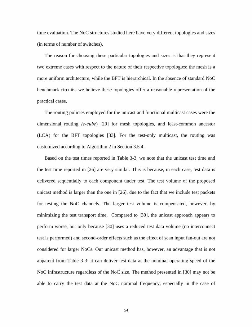
54
time evaluation. The NoC structures studied here have very different topologies and sizes
(in terms of number of switches).
The reason for choosing these particular topologies and sizes is that they represent
two extreme cases with respect to the nature of their respective topologies: the mesh is a
more uniform architecture, while the BFT is hierarchical. In the absence of standard NoC
benchmark circuits, we believe these topologies offer a reasonable representation of the
practical cases.
The routing policies employed for the unicast and functional multicast cases were the
dimensional routing (e-cube) [20] for mesh topologies, and least-common ancestor
(LCA) for the BFT topologies [33]. For the test-only multicast, the routing was
customized according to Algorithm 2 in Section 3.5.4.
Based on the test times reported in Table 3-3, we note that the unicast test time and
the test time reported in [26] are very similar. This is because, in each case, test data is
delivered sequentially to each component under test. The test volume of the proposed
unicast method is larger than the one in [26], due to the fact that we include test packets
for testing the NoC channels. The larger test volume is compensated, however, by
minimizing the test transport time. Compared to [30], the unicast approach appears to
perform worse, but only because [30] uses a reduced test data volume (no interconnect
test is performed) and second-order effects such as the effect of scan input fan-out are not
considered for larger NoCs. Our unicast method has, however, an advantage that is not
apparent from Table 3-3: it can deliver test data at the nominal operating speed of the
NoC infrastructure regardless of the NoC size. The method presented in [30] may not be
able to carry the test data at the NoC nominal frequency, especially in the case of

55
large-size architectures, when the fan-out of the scan input will increase significantly and
the maximum switching rate of the scan-chains accordingly.
Comparing the test times with multicast, the superiority of the multicast test data
transport is evident. The improvement in test speed range from 2X for the case of
small-size NoCs, to 34.5X for large size NoCs. As with the unicast transport method, the
multicast mechanism is able to transport test data at the nominal operating speed of the
NoC, thus making possible at-speed transport of test packets test with no additional cost.
Another important quality metric of our test methodology is the silicon area overhead
of the unicast and multicast test data transport mechanisms. There are two major
components that contribute to the overhead of the schemes. The first is the test control
(TC) unit, in charge of test packet processing, test input data injection to CUT inputs, and
test output comparison. The second is the multicast wrapper unit (MWU) which
implements the single-source, multiple-destination test data transport feature. We
compare the gate-count of the test-only multicast solution with the gate-count of the
functional multicast implementation.
Table 3-4 shows the gate count for the unicast, test-only multicast, and functional
multicast implementations. The gate-count for the unicast case corresponds to the test
control (TC) blocks, which are identical for a given topology. The TC blocks differ for
different topologies, since they have to handle a different number of components (FIFOs,
routing blocks, inter-switch links) adjacent to a switch. The gate-count reported for the
test-only multicast is the sum of TC gate-count and the MWU gate-count, averaged for
all the switches in the respective NoC instance. Averaging is needed because the test-only
multicast feature is implemented selectively, only for those ports per switch which are

56
involved in multicast data transport. The list of ports that need to be connected to the
MWU for each switch was obtained by examining the optimal test scheduling as
computed using Algorithms 1 and 2 presented in Section 3.5.4. The last column in Table
3-4, labeled %diff, shows the percent difference between the gate-count per switch of the
functional multicast implementation (column 4) and the test-only one (column 3).
The absolute area required to implement the proposed test mechanisms is acceptable,
especially when compared to the typical gate-count of a NoC switch (around 30,000
gates, as reported in [25], [46] and [47]).
Table 3-4: Gate count and comparison for the proposed test mechanism (per switch)
NoC type & sizeAlgorithm 1unicast test
[gates]
Algorithm 2multicast test
[gates]
Functionalmulticast[gates]
%diff
4 x 4 524 825 1025 19.5
8 x 8 548 792 1025 22.7Mesh
16 x 16 576 721 1025 29.6
6 693 816 1210 32.5
28 718 771 1210 36.3BFT
120 736 722 1210 40.3
Moreover, when multicast data transport is adopted, by implementing this feature
selectively for only the switch ports on multicast paths, significant area reduction can be
obtained (up to 40% when compared to the functional multicast realization, for the NoC
instances in our experiments).
The MWU hardware introduces a certain amount of delay in the data path of the
packets, equivalent to the delay of a demultiplexer/multiplexer pair as shown in Fig. 3-4.
This delay adds to the delay of the routing block RLB. Through gate level design and
analysis, the equivalent delay of the MWU is found to be equal to 3 FO4 (fan-out of four)
delay units. The typical delay of the RLB block is around 6 FO4 units [54]. Therefore,

57
the total delay of the RLB and MWU blocks is around 9 FO4 units, which fits well within
the limit of 10-15 FO4 units according to ITRS projected trends for clock speed of high-
performance multi-processors.
Table 3-5 shows the amount of time required to obtain an optimal scheduling running
the two algorithms presented in Section 3.5.
Table 3-5: Test scheduling run-times
NoC type &size
Algorithm 1 - unicastrun-time [s]
Algorithm 2 – multicastrun-time [s]
4 x 4 4 3
8 x 8 12 9Mesh
16 x 16 33 27
6 2 2
28 7 5BFT
120 15 11
The run-times in Table 3-5 do not include the time required to run the ATPG tool to
generate the test patterns for the logic blocks, since this has to be done irrespective of the
particular test transport implementation. Clearly, the test scheduling methods do not
require significant run-times, even for relatively large NoCs (256-nodes mesh,
120-switch BFT).
3.7 Summary
A novel method for testing the communication fabric of network-on-chip (NoC)
based multi-processor systems-on-chip (MP-SoCs) was presented in this chapter. The
novelty of this method lies in the reuse of the NoC fabric for test data transport in a
recursive manner, and in exploiting the inherent parallelism of the NoC architectures for
speeding the test data transport and reducing the test time. Test scheduling algorithms
were developed for two types of test data transport: sequential (unicast) and concurrent

58
(multicast). The proposed methods integrate the test of all types of NoC components
(buffers, links, and routing blocks) in a unified fashion. The efficiency of the test
methods was evaluated for synthetic NoCs of different topologies and sizes. The results
of this assessment show significant speed-up of test data delivery compared to previously
proposed NoC test methods, from 2X for small-size NoCs, up to 34X for larger networks.

Chapter 4
4 Fault-tolerance Techniques for Networks-on-chip 3
Fault tolerance in a design implies that the design can withstand certain static and
dynamic faults, and still operate correctly. Although all possible fault mechanisms are not
usually covered, the most important ones are addressed to greatly increase the reliability
of a system.
Fault tolerant design of network-on-chip communication architectures requires the
addressing of issues pertaining to different elements described at different levels of
design abstraction – these may be specific to architecture, interconnection,
communication and application issues. Assessing the effectiveness of a particular fault
tolerant implementation can be a challenging task for designers, constrained with tight
system performance specifications and other constraints. In this chapter, a top-down view
of fault tolerance methods for NoC infrastructures is provided, and two novel metrics
used for estimating their quality are proposed: detection latency and avoidance latency.
The use of these metrics is illustrated by simulating a few simple but realistic fault
tolerant scenarios.
3 This chapter is based on work published in:1. C. Grecu, L. Anghel, P. P. Pande, A. Ivanov, R. Saleh, "Essential fault-tolerance metrics for NoC
infrastructures", 13th IEEE International Online Testing Symposium (IOLTS), IOLTS’07 9th -11th
July, 2007.2. C. Grecu, A. Ivanov, R. Saleh, E. S. Sogomonyan, P.P. Pande, "On-line fault detection and
location for NoC interconnects", 12th IEEE International Online Testing Symposium (IOLTS),IOLTS06, July 2006.

60
4.1 Introduction
A major cause affecting the reliability of the VLSI global interconnects is the
shrinking of the feature size, which exposes them to different faults of a permanent
(static), transient (dynamic) or intermittent (dynamic) nature. Static faults include opens
and shorts in the wires and missing vias in the interconnect, and a variety of well-known
faults in logic and memory. Among the dynamic failure mechanisms we can enumerate
factors such as crosstalk, electromigration, electromagnetic interference, alpha particle
hits, and cosmic radiations [55]. These phenomena can alter the timing and functionality
of the NoC fabrics and thus degrade their quality-of-services (QoS) characteristics or,
eventually, lead to failures of the whole NoC-based system. Providing resilience from
such faults is mandatory for the operation of NoC-based chips.
Traditionally, error detection and correction mechanisms are used to protect
communication subsystems against the effects of transient malfunctions. Designers must
carefully weigh the hardware cost of implementing such mechanisms for the on-chip data
communication infrastructures against the potential benefits they can bring [56] [57].
Complex error detection and correction (EDC) schemes may require additional energy
dissipation and area overhead, and can affect the performance of SoC communication
architectures in terms of throughput and latency. Other approaches for fault-tolerant on
chip communication include stochastic communication, adaptive routing, and different
hybrid schemes that combine spatial and temporal redundancy for achieving fault
tolerance.
Metrics for fault-tolerant systems are well-established and have been used extensively
in design of distributed computing systems. Recent research in fault-tolerant NoC fabrics

61
proposed metrics that are specific to message-passing on-chip communication systems
for evaluating the effectiveness of new and existing fault tolerance methods. In the
absence of widely accepted metrics, it is difficult for NoC designers to assess the fault-
tolerant capabilities in a quantitative manner. This is especially true when comparing
different fault-tolerant techniques with the objective of determining which one can
deliver the best performance within acceptable costs.
One option for evaluating the fault-tolerance (FT) capabilities of a system is to
measure the degree of hardware and software redundancy (spatial and temporal), which is
an inherent property of most NoC architectures. While redundancy by itself is a useful
measure, it is incomplete in that different systems can exploit redundancy in more or less
efficient ways. It is therefore preferable to have metrics that can measure the effective
fault tolerance as it influences the required performance in accomplishing the task of
transporting information across the NoC fabric. Based on the above considerations, the
scope of this chapter is to present traditional FT metrics in the novel context of NoC
systems, and use them synergistically with newly proposed metrics, in order to measure
the effective fault tolerance in the context of overall system performance for NoC
subsystems.
The quest for on-chip fault-tolerant communication started well before the NoC
paradigm emerged as a solution for integrating large MP-SoCs. Design techniques for
fault-tolerant on-chip busses are found in [58], where a particular form of duplication is
used to detect and correct crosstalk and transient faults, and [59], where different error
recovery mechanisms from simple retransmission to correction/retransmission are
analyzed in terms of power/area figures.

62
The NoC infrastructures are characterized by more complex topologies (relative to
buses), with higher degrees of connectivity. Moreover, in the NoC paradigm, data is
transferred across the chip by employing some form of packet switching, where sent data
is tagged with additional flow control information [20]. The additional hardware and/or
information redundancy, offers significant potential for implementing different
fault-tolerant strategies. Hardware redundancy can be exploited by using multiple paths
to transport data between source and destination cores, e.g., in the case of adaptive
routing methods [60], or stochastic communication [61] [62]. In [61], the total time to
complete the application (a Fast Fourier Transform algorithm) in the presence of faults is
another performance measure of the FT method. General-purpose metrics used in [61]
and [62] are energy consumption and area cost, which are fully usable and relevant.
Information redundancy can be implemented by means of error detection/correction
schemes, where additional control bits can be used to detect the presence of errors and
eventually to reconstruct the original data. When the presence of errors in the data stream
is detected but not corrected, error recovery is usually performed through retransmission,
which is one of the possible forms of temporal recovery [63].
In practice, temporal and spatial data redundancy is often used to achieve the fault
tolerant goals. Ultimately, designers must assess the effectiveness of the FT
implementation in the context of the NoC performance specification. This information
must be readily available and quantifiable such that, if a specific FT implementation
cannot be accommodated while still meeting the performance specification of the NoC
medium, it can be eliminated from the set of potential FT realizations at early stages of
the design process.

63
Most of the previously published works on the issue of FT in NoCs present methods
at algorithm or circuit level, and then proceed to assess them relative to an ad-hoc set of
parameters that may be more or less relevant to the specifics of an on-chip data transport
mechanism.
In [61] and [62], the authors propose probabilistic communication schemes based on
probabilistic broadcast and random walk, respectively. In these schemes, multiple copies
of the same message are transmitted following different paths, selected randomly from
the set of possible routes between communicating pairs of cores. When transient or
permanent faults manifest themselves in the NoC fabric, the affected message replicas are
discarded. Eventually, from the set of redundant messages, one that is error-free may
reach the destination, completing a successful transmission. Message latency is correctly
identified in both works as an important measure for evaluating the impact of the FT
solution. However, there are many factors that can affect message latency, other than the
specific FT implementation, such as traffic distribution (spatial and temporal), buffer size
and buffer management, flow control, etc. The contributions of all these factors towards
message latency are generally inter-dependent, and it is quite difficult to separate their
individual effects. As such, it is difficult to estimate with acceptable accuracy the effect
of the FT method on latency, isolated from the other factors.
In [64], a new metric to characterize fault-tolerant NoCs is proposed, called message
arrival probability (MAP). For a pair of tasks (processes) that exchange messages across
the NoC, MAP is defined as the fraction of successfully transmitted messages. This
metric is useful for assessing NoC performance when tight bounds are imposed on its
capability of transmitting error-free messages.

64
A different category of FT metrics relates to topology characteristics that can
potentially offer FT properties. In particular, connectivity is used to express the ability of
an interconnection network to offer multiple paths among its communicating nodes [65].
This metric is useful, but only when combined with the flow control mechanism that can
exploit the degree of connectivity in a more or less efficient manner.
When dedicated spare routers or links are employed for achieving fault tolerance, the
amount of spare elements can give an estimate of the NoC’s FT capabilities. As for the
connectivity, the amount of spares is only offering information about the NoC’s potential
fault tolerance, rather than its actual ability.
Various coding schemes were proposed for providing error resilience to on-chip
communication infrastructures [57] [66]. A comprehensive comparison and evaluation is
carried out in [67] for detection-only and single-error correcting codes, combined with
retransmission for data recovery. The effect of locating the recovery points in the NoC
topology (e.g., end-to-end or switch-to-switch recovery) is also studied and evaluated.
The metrics used in [66] and [67] quantify the effect of error recovery schemes on NoC
parameters such as data latency, area overhead, and energy consumption, under specific
conditions of NoC operation.
The types of approaches for determining the efficiency of FT schemes based on their
effect on NoC performance parameters, under specific operating conditions, have the
drawback that they only deliver information for a set of inter-dependent operating
conditions (i.e., a given NoC hardware instance, specific traffic distributions and flow
control protocols).

65
We propose to complement these measuring practices by including the measurement
of the intrinsic performance of the particular FT scheme in terms of its capability of
avoiding failed states, detecting a failure, or recovering from a failed state. Combined
with performance parameter measurement in presence of FT mechanisms, the metrics
proposed and evaluated in this chapter give the designers a better understanding of the
trade-offs involved in designing high-performance, fault-tolerant networks-on-chip.
4.2 Traditional fault-tolerance metrics
Traditional engineering methods that address design of fault tolerant systems use
reliability and availability analysis to characterize these systems and their components
[68]. Reliability is defined as the probability with which a system will perform its task
without failure under specified environmental conditions over a specified time duration.
Thus, the MTBF (Mean Time Between Failures) parameter is used as a representation of
reliability, and is calculated as:
Total operating timeMTBF
No.of failures encountered (4.1)
Another metric used for evaluation of fault tolerant systems with repair/recovery
capabilities is represented as MTTR (Mean Time to Repair):
Total time spent for repairsMTTR
No. of repairs (4.2)
Based on MTBF and MTTR, the availability of a system can be used to measure the
impact of failures on an application, and is defined as:
100%MTBF
AvailabilityMTBF MTTR
(4.3)
While useful at the system level, these metrics may overlook important properties of
fault tolerant NoC subsystems. One such property that is misrepresented by use of MTBF

66
is the capability of a NoC protocol to rapidly recover from failures. Even in the case
when the number of failures is high (which indicates a low, undesired MTBF), if the
recovery can be performed quickly (e.g., through flit-level recovery [67] [69]), the impact
of failures may be minimal and, therefore, it may not affect the application at all. For the
same reason, the availability of the NoC subsystem in such a condition can be
misinterpreted if viewed only by Eq. (4.3).
Another drawback of these generic, system-level metrics is that they represent average
values. In the case of NoC fabrics that must meet tight quality of services (QoS)
requirements in the presence of failures, the average values are not useful since the
performance constraints (in terms of guaranteed latency per message or available
throughput) have to be met for all possible instances, not only on an average basis.
While there is little doubt that fault tolerance is a desirable and useful property of NoCs,
designers need simple, readily available metrics to be able to characterize FT methods in
the context of the specific NoC implementation. We introduce these metrics relative to
the NoC’s ability to detect the occurrence of faults and recover from failures. The metrics
proposed in this work aim to address the issue of characterizing the effectiveness of fault
tolerance schemes for NoC communication subsystems in the context of the specific QoS
requirements that designers face in their implementation. They are not intended to
substitute the existing metrics, but to complement them by offering a more detailed view
of the properties of different fault-tolerance methods. We illustrate how the metrics
defined here can help designers gain more insight on the actual performance of fault
tolerant implementations related to NoC architectures. The metrics proposed in this
chapter are described in Section 4.3 and evaluated in Section 4.4.

67
4.3 Fault-tolerance metrics for network-on-chip subsystems
Before defining the set of metrics forming the object of this work, we need to
differentiate between different hierarchical abstraction levels for achieving resilience to
failures. There are five key elements in a comprehensive approach to fault tolerant
design: avoidance, detection, containment, isolation, and recovery. Ideally, these are
implemented in a modular, hierarchical design, encompassing an integrated combination
of hardware and software techniques. Moreover, the fault tolerant techniques can be
applied at different layers from the set of ISO/OSI layers [21] that the NoC may
implement, resulting in numerous possibilities for fine tuning the performance of the FT
implementation by combining the (sub)set of FT elements with the (sub)set of NoC
layers. As an example, error detection may be implemented in the data layer, and
recovery may be realized either in the data layer (e.g., if an error correcting code is used)
or at the application layer. In a more generic approach, the partitioning and derivation of
requirements, and the partitioning and implementation of fault/failure management
techniques must be realized in a hierarchical fashion. For each hierarchical level, the
existence of appropriate metrics allows the designers to have full control and
understanding of the implications that a particular fault-tolerant implementation will have
on the operation of a NoC subsystem. In this chapter, two novel metrics for evaluating
the performance of fault-tolerant mechanisms are proposed: detection latency and
avoidance latency.
For illustrating the value of the metrics proposed here and their usability, a simple
example of an application A running on a NoC-based multi-processing system is
considered. The application uses two processes P1 and P2 on two different processing

68
cores, as shown in Fig. 4-1. Ideally, processes P1 and P2 use the NoC subsystem to
communicate with each other along the path shaded in grey. However, a different path
may be taken if there is a fault on the ideal path.
Figure 4-1: Processes communicating across a NoC fabric
layout & device level(physical layer)
fl it/packet level(data layer)
end-to-end (network/transport layer)
app lication level(application/session layer)
Faults:- type - source - rate - impact
D/R
D/R
D/R
D/R
Figure 4-2: Hierarchical partitioning for fault tolerant NoC designs.

69
Faults can be detected and recovered in many ways. Using a layered representation of
the data communication in a NoC-based system, and considering a subset of the standard
OSI layers [70], Fig. 4-2 shows the propagation of faults from the physical level (faults
affecting low-level device functionality) to the application level (faults affecting the
software application running on the NoC-based system). At each level in the hierarchy,
faults can be characterized by type, source, frequency of occurrence, and impact. At the
lowest level (physical), it is assumed that a fault results in a degraded operation of the
respective component. For example, a wire short or open, or a missing via could occur at
this level. Then, either repair is performed or the problem is passed on to the next level.
That is, at each level, detection and recovery have associated costs and performance
penalties. If it is not always cost effective to detect-and-recover (D/R) at the lowest level,
the fault manifests as a local error/failure which propagates to the next higher level,
where the corresponding FT technique is evaluated again relative to performance and cost
effectiveness. The objective of this hierarchical partitioning is to provide cost-effective
handling of error/failures while satisfying system requirements. The hierarchical
approach can provide back-up at higher levels for faults which, for any reason, are not
handled at lower levels. In the case of Fig. 4-1, if a low level-fault occurs, an alternate
route can be taken between P1 and P2 (along the dashed line) to avoid the problem by
addressing it at the network/transport layer. This comes at the cost of higher data
transport latency due to the non-optimal path-length. Generally, the higher the level in the
hierarchy, the longer it takes to contain and/or recover from the effect of a failure, but
there are certain advantages with respect to area cost and power dissipation. For real-time
NoC systems, time is the critical factor for specifying the performance of the FT

70
implementation. Designers must decide on the effectiveness of a particular method by
knowing how quickly faults must be detected, how quickly they have to recover from the
occurrence of a fault, how long an error can exist in the NoC infrastructure without
impairing/compromising system performance. This is the motivation for new metrics for
fault-tolerance in NoCs, especially in cases when QoS constraints must be satisfied.
First, based on the example application in Fig. 4-1 and considering a hierarchical
implementation as in Fig. 4-2, we define metrics for the five elements of comprehensive
fault-tolerant methods.
(a) Avoidance
Fault-avoidance techniques can be realized through information redundancy (by
means of error correcting codes for NoCs) or hardware redundancy (n-modular
redundancy being a typical example). Depending on the targeted number of errors to
correct, coding/decoding hardware blocks may require a certain number of cycles to
perform their operation. The associated time overhead adds to the total latency of the data
being transported across the NoC fabric. Additionally, area and power overhead must be
considered.
We define the time overhead of an avoidance scheme, Tav,ov, as the difference
between data latency with (Latav) and without (Lat) fault avoidance:
Tav ov = Latav – Lat (4.4)
The difference between various implementations of this concept can be significant
relative to this metric. In the example in Fig. 4-1, if coding/decoding functions are
implemented at each switch on the path between P1 and P2 (switch-to-switch avoidance),
the resulting time overhead will be significantly higher than in the case where only

71
end-to-end avoidance is implemented (i.e., data is encoded at the source and decoded at
destination). Ideally, latency insensitive protocols and link pipelining techniques mitigate
the effect of the extra latency cycles.
(b) Detection
The next hierarchical level in a fault-tolerant design is detection of faults that were not
handled by the avoidance mechanism. Detection is built in most error-correcting codes,
which generally can provide information regarding the number of un-corrected faults,
when the correction mechanism fails (or is not even present in the particular
implementation). Fault detection is then used to assess the need for recovery from
potentially uncorrected fatal failures. The quicker the detection mechanism signals the
presence of uncorrected faults, the quicker the recovery can be initiated. We define the
detection latency Tlat as the amount of time between the moment a fault occurs and the
moment it is detected. Going back to our example in Fig. 1, fault detection may be
performed by the processes P1 and P2 whenever data is received (end-to-end detection), at
the input ports of the intermediate switches (switch-to-switch detection), or at each
switch input/output port (code-disjoint detection). In each case, the detection latency Tlat
is different and the impact on the performance of the FT system varies accordingly.
(c) Containment
Fault containment is concerned with limiting the impact of a fault to a well-defined
region within the NoC. Error containment refers to avoiding the propagation of the
consequences of a fault, the error, out of this defined region. Fault containment regions
(FCR) may be defined with variable resolutions, directly correlated with the quality and
resolution of the fault detection mechanism. For the case of Fig. 4-1, and assuming an

72
end-to-end detection mechanism, the fault containment region can be defined as the
entire shaded route between the cores where processes P1 and P2 are being executed. The
size of the fault containment regions can be decreased by employing more accurate fault
detection schemes, such as switch-to-switch or code-disjoint detection. It is essential that
FCR be independent in the sense that a fault occurring in a FCR does not affect a
different FCR. In this respect, if two routes between cores/processes P1 and P2 can be
found that are on independent FCRs, and a fault is detected on one of the routes, the other
route can be used to provide an alternative path between processes P1 and P2 (represented
as a dashed line in Fig. 4-1).
(d) Isolation
The independency of fault containment regions can only be achieved if an effective
isolation method can be provided, which can guarantee that the effect of a fault occurring
in a FCR does not propagate to another FCR. At the physical layer, in the case of
permanent faults, isolation can be accomplished by marking or disconnecting the faulty
NoC components (links, switches, routes) and avoiding their use until, eventually,
hardware recovery/repair can be performed through reconfiguration. At higher layers,
erroneous data packets can be dropped on the fly or at the destination process, such that
they are not allowed to interfere with the rest of the data and propagate at application
level.
(e) Recovery
The ultimate goal of fault tolerant schemes is to provide means to recover from
occurrence of failures. For fault-tolerant, QoS constrained NoCs, it is important to
recover from failures within the time budget allowed by the QoS specifications. Late

73
recoveries, even when successful, are not acceptable, since they lead to
out-of-specification behaviour of the NoC subsystem. Consequently, we define recovery
time (Trec) as the amount of time that passes between the detection of a fault and recovery
from the corresponding failure. A simple form of attempting recovery of erroneous data
flowing between processes P1 and P2 is to provide a hardware correction at lower layers,
or a retransmission mechanism at higher layers where, upon detection of an error, an
automated retransmission request (ARQ) is generated and an error-free copy of original
data is resent from the source process.
4.4 Metrics evaluation
The use of the metrics defined in this work is illustrated by running simulations of a
few detection and recovery schemes on a 4x4 NoC fabric, as depicted in Fig. 4-1. A
cycle-accurate, flit-level simulator is used [101], with messages injected with equal
probabilities by all NoC cores (i.e., uniformly distributed random traffic). The value of
these metrics will be illustrated with an example.
In all simulations, messages are organized in 16 flits each, and are transferred across
the NoC medium following the dimension-order (e-cube) routing algorithm, where
messages are first sent along the x direction of the topology, then along the y direction
towards the destination core. The injection rate is varied uniformly. Faults are injected
randomly, on a flit-per-cycle basis, i.e., in each cycle, flits may be marked as erroneous
with equal probabilities, regardless of their current location in the NoC fabric.
In this set of experiments, we are mainly interested in detection and recovery
estimation. We consider the following cases for fault detection scenarios:

74
- end-to-end (e2e) detection: the errors are detected at the destination cores. Each flit is
checked for errors upon reception and, if found erroneous, the detection latency is
calculated as the time difference between the fault injection moment and flit arrival time.
- switch-to-switch (s2s) detection: error checking is performed at each input port of the
switches, for each flit traveling across the NoC.
- code-disjoint (cdd) detection: flits are checked for errors at both input and output ports
of the NoC switches.
Figure 4-3: Average detection latency for end-to-end (e2e), switch-to-switch (s2s), andcode-disjoint (cdd) detection schemes.
Fig. 4-3 shows the average detection latency for the three detection mechanisms
considered here. Flit error rate is set at e=10-10, i.e., in each cycle, for each flit, the
probability of being flagged as erroneous is 10-10 [71]. The e2e detection is the poorest
performer relative to detection latency, since the messages must travel all the way from
source to destination before an eventual error being detected. The cdd mechanism

75
performs best, due to the fact that error detection is performed at each input/output of the
switches.
Next, two recovery methods are simulated, both based on retransmission of erroneous
messages. The first scheme is a message-level, equal-priority retransmission. Upon
detection of an erroneous flit, an ARQ message is generated at the destination core. For
ease of implementation, the ARQ message is injected into the network immediately, once
all the flits of the erroneous message have been completely received. If more flits in a
message are erroneous, only one ARQ message is generated. The ARQ is sent towards
the source of the erroneous message and handled as any other regular message by the
NoC environment. The case where ARQ messages themselves are affected by errors is
not considered here. There are three types of messages in this scheme: regular messages,
ARQ messages, and retransmitted messages. They all have equal priorities, and are
treated similarly when traversing the NoC. We call this method equal priority recovery
(epr).
For speeding up the recovery process, we consider a second retransmission-based
recovery scheme, where ARQ and retransmitted messages have higher priority than the
regular messages. When contention arises, regular messages will wait for ARQ and
retransmitted messages to be processed. This allows faster transport of the latter
messages types, and therefore speed-up the recovery process. We call this method
priority-based recovery (pbr).
The next experiment measures the recovery latency for a few combinations of
detection/recovery schemes. Ideally, we would like to isolate the detection and recovery
mechanisms, and report individual performance figures for the recovery phase only. In
76
practice, this is difficult due to the two processes being inter-dependent. In our
experiments, the inter-dependency is caused by the need to manage the erroneous
messages in a realistic fashion, i.e., upon detection of an erroneous flit, the corresponding
message continues to be transported toward its destination and, eventually, interact with
ARQ and retransmitted messages. This causes erroneous messages to continue to traverse
the NoC after error detection and keep NoC resources occupied, effectively reducing the
NoC capability to transport ARQ and retransmitted messages with maximum efficiency.
Figure 4-4: Average recovery latency for equal priority recovery (epr) and priority basedrecovery (pbr).
The average recovery latencies for the two recovery methods considered in our
experiments are shown in Fig. 4-4. The flit error rate is set to e=10-10 for all simulation
runs. Note that the pbr method offers better recovery latency due to preferential
processing of ARQ and retransmitted messages. The advantage of priority-based
recovery is more apparent at higher injection rates, where the ARQ and retransmitted
messages are able to travel faster than the regular messages waiting in queue buffers for
available resources. Also, the pbr scheme can support tighter QoS requirements in terms

77
of minimum latency in presence of errors.
In the last experiment, we study the effect of varying the flit error rate e on the
average recovery latency, for the pbr scheme. In this experiment, the message injection
rate was set constant to a non-saturating value of 0.1 flits/cycle/core. A high flit error rate
will cause the generation of numerous ARQ and retransmitted messages, which will
effectively cause an increase of the NoC traffic. Similarly, a high injection rate will
cause, even in the error-free case, an increase in latency due to message congestion.
Therefore, simulations are performed at a low, non-saturating injection rate, at which the
variation of message recovery latency is principally affected by the error rate e.
The results shown in Fig. 4-5 indicate that the system can reliably recover from
failures at flit error rates up to approximately e=10-9. At this point, the recovery latency
starts to increase significantly, and reaches values that may not be compatible with the
QoS specifications of the system. The recovery latency is influenced by both the flit error
rate and message injection rate. For higher message injection rates, the nature of the
curves in Fig. 4-5 remains the same, but with a higher flat plateau at low flit error rates
(due to increased average message latency), and a faster increase of recovery latency with
increasing flit error rate. For a complete characterization of a practical case, simulations
would have to cover a wider range of traffic conditions.

78
Figure 4-5: Average recovery latency for pbr scheme with variable flit error rate
The advantage of using the detection and recovery latencies as defined in this work
becomes apparent by observing that using experiments similar to the ones presented here,
designers are able to isolate the performance figures of fault tolerant methods from the
environmental conditions (represented by traffic conditions in our experiments).
As an example, the design specification of a NoC fabric such as the one in Fig. 4-1
may require an average recovery latency of 30 cycles for a message injection rate of up to
0.1 flits/cycle/core, at a flit error rate of up to e=10-10. Based on the simulation results in
Fig. 4-4 and 4-5, the end-to-end (e2e) schemes can be eliminated from the set of potential
candidates for FT implementations, since their average recovery latency is greater than
the required value of 30 cycles.
Finally, we estimate the message arrival probability (MAP) associated with the three
detection scenarios, for the pair of communicating processes P1 and P2. This is an
indication of how well the three schemes perform when application A in Fig. 4-1 has tight
bound imposed on the quality of communication between processes P1 and P2 in terms of

79
the ratio of successfully transmitted messages (targeted QoS [72]). In Fig. 4-6, we plot
the average message latency versus bound on MAP under traffic assumptions stated
earlier in this section. In this set of experiments, flit error rate was set at e=10-6, at a
message injection rate close to network saturation.
Figure 4-6: Average message latency vs. bound on MAP.
Note that when the required MAP is increasing towards 1, the average message
latency increases significantly. This indicates that, when the application requires a MAP
close to 1, the simple recovery techniques presented here may not suffice, and more
advanced FT techniques need to be employed. Also, a complete characterization of
particular FT techniques would involve additional application metrics under
application-specific traffic conditions.
To illustrate how the metrics presented in this chapter can be used by NoC designers
to select an appropriate FT technique when a NoC system is designed with QoS
constraints, consider the case of two application tasks T1, T2 mapped onto processors P1,
P2, respectively, in a 4X4 mesh NoC, as shown in Fig. 4-7.

80
Figure 4-7: Processes P1, P2 mapped on a mesh NoC with QoS communication constraints.
The QoS specifications for the two tasks are expressed as follows:
“The maximum allowed flit latency between processes P1 and P2 is 60 clock cycles, for
a message injection rate of up to 0.3 message/cycle/process and a maximum flit error
rate of 10-10.”
The task of the designer is to find a combination of error detection and recovery
methods that satisfies the above constraint, while factoring in the cost in terms of area
overhead. For simplicity, these costs are assumed to be known and ordered as in Fig. 4-8
for the set of detection and recovery methods considered earlier in this chapter.
code-disjoint
switch-to-switch
low
med
ium
high
end-to-end
low
med
ium
high
Figure 4-8: Performance and cost of detection techniques.
For determining what combination of error detection and latency is the most

81
appropriate, the designer will extract the latency numbers performing analysis or
simulations, and then choose the pair whose added latencies satisfy the QoS requirement.
For illustration, the latency metrics for the detection/recovery methods considered in this
chapter and applied to the two communicating processes P1, P2 in Fig. 4-7 are shown in
Tables 4-1 and 4-2, respectively.
Table 4-1: Detection latency (10-10 flit error rate)
Traffic load (message injection rate, [message/cycle/process])
0 (no-load) 0.1 0.2 0.3
cdd 3 3 3 4
s2s 4 4 5 6
e2e 21 21 22 24
Table 4-2: Recovery latency (10-10 flit error rate)
Traffic load (message injection rate, [message/cycle/process])
0 (no-load) 0.1 0.2 0.3
epr 42 42 45 58
pbr 42 42 45 51
Adding the corresponding cells in Tables 4-1 and 4-2, one can determine which
detection/recovery pair can be successfully used. Two options are available to the
designer in this example: cdd + pbr and s2s + pbr. All other combinations exceed the
latency limit imposed by the QoS constraint. Factoring in the higher area cost of the
detection techniques as shown in Fig. 4-8, the solution of choice is s2s + pbr, which

82
requires a lower implementation cost. Clearly, the separation of fault-tolerance
mechanisms and differentiation of the latency metrics provides greater visibility in
selecting the optimal method.
4.5 Summary
The need for fault-tolerant features in NoC communication fabrics is recognized by
academic and industrial communities, and different implementations are possible to
address the challenges of providing fault-tolerant communication in NoC subsystems. It
is, however, difficult for designers to choose a particular FT scheme due to lack of
metrics that can express the intrinsic effectiveness of a FT method, and not only its effect
on generic performance parameters such as latency, throughput, and power consumption.
We have presented a comprehensive, unified view of fault tolerant methods for NoC
subsystems, with hierarchical partitioning that makes possible mapping the elements of a
FT implementation on the generic layered structure of network-based communication
systems. We presented two novel metrics (detection latency and recovery latency) that
assess the capability of a NoC subsystem to quickly detect the presence of a fault and
recover from failures in a speedy manner. The use of these metrics was illustrated with a
set of simulations. These metrics are intended to complement the generic, application
oriented (throughput, latency) and resource oriented (area overhead, power consumption)
metrics.

83
Chapter 5
5 Fault-tolerant Global Links for Inter-core Communicationin Networks-on-chip 4
5.1 Introduction
In this chapter, we propose a method to improve the yield of global links of NoC-
based chips by using redundant upper-level wires interconnected with the low-level metal
lines in a sparse matrix configuration. The global NoC links are defined as the lines used
to transfer the intercore signals (inter-router or router-to-PE). A yield improvement
technique targeted specifically at these links is developed. The structured nature and
functionality of the SoC interconnect infrastructures render them particularly suitable for
the implementation of these features, similar to the case of memory blocks, where yield
enhancement and defect tolerant techniques have become common practice [15] [55] for
some time already. According to the discussion and classification in Chapter 4, the
fault-tolerant solution here is a low-level fault-tolerant technique, placed at the physical
level, whose containment region is the corresponding NoC link. Its performance in terms
of fault detection time and recovery speed through link reconfiguration is outlined in
Section 5.8 of this chapter.
4 This chapter is based on work published in or submitted to:1. C. Grecu, A. Ivanov, R. Saleh, P.P. Pande, "NoC interconnect yield improvement using crosspoint
redundancy", IEEE Symposium on Defect and Fault Tolerance in VLSI Systems, 2006, DFT '06,Oct. 2006.
2. C. Grecu, D. Sengupta, P.P. Pande, A. Ivanov, R. Saleh, “Self-repairable SoC communicationlinks using crosspoint redundancy”, IEEE Transactions on VLSI, under review, submitted Feb.2008.

84
The method described in the following sections is based on the use of sparse regular
crossbars, which are a particular class of generalized connectors. The novel features of
our method are two-fold: first, we provide a mechanism to test the inter-core links
post-fabrication at start-up or during run-time and detect the faulty wires. Second, we
design a reconfiguration scheme that selects a set of fault-free wires to set-up the
connections between cores. The reconfiguration scheme is designed such that every
possible combination of fault-free wires yields closely matched delays, with the benefit
of ensuring consistent, uniform link speed across a wide range of defect sites.
A widely-used technique for achieving fault-tolerance in computing systems is the
N-way modular redundancy (NMR) [63]. This is based on replicating the component a
number of times (three or more) and employing voting mechanisms to decide which of
the replicas delivered a fault-free output. Generally, this technique brings a high hardware
overhead due to the number of replicas involved. In the particular case of fault-tolerant
NoC communication links, the use of NMR is prohibitive due to large interconnect
overhead, which can lead to wire congestion and routing difficulties. Our solution is more
fine-grained than the classic NMR, and delivers a methodology for yield tuning, test, and
reconfiguration.
5.2 Related work
Sparse crossbars were originally proposed in [73] for designing high-performance,
hardware efficient concentrators and distributors for interconnection networks. Their
applications range from computer networks [74] to multi-processor systems [75] and
instrumentation networks [76]. Fault tolerance of global SoC interconnects was addressed
by different groups proposing error recovery schemes based on error detection and
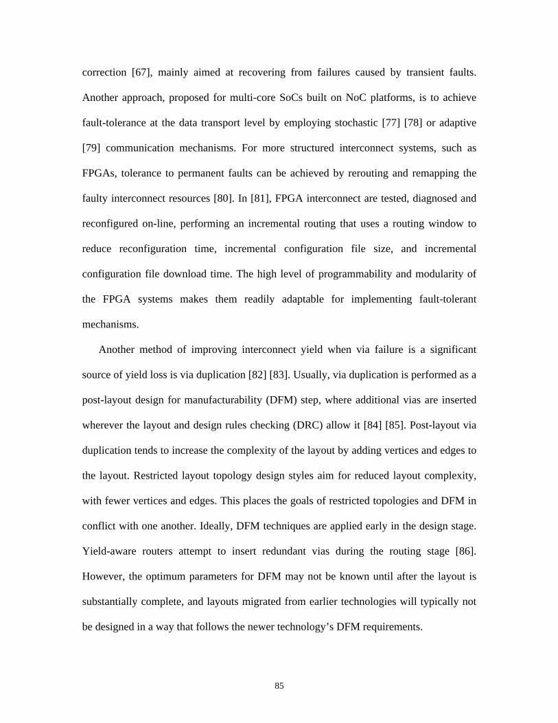
85
correction [67], mainly aimed at recovering from failures caused by transient faults.
Another approach, proposed for multi-core SoCs built on NoC platforms, is to achieve
fault-tolerance at the data transport level by employing stochastic [77] [78] or adaptive
[79] communication mechanisms. For more structured interconnect systems, such as
FPGAs, tolerance to permanent faults can be achieved by rerouting and remapping the
faulty interconnect resources [80]. In [81], FPGA interconnect are tested, diagnosed and
reconfigured on-line, performing an incremental routing that uses a routing window to
reduce reconfiguration time, incremental configuration file size, and incremental
configuration file download time. The high level of programmability and modularity of
the FPGA systems makes them readily adaptable for implementing fault-tolerant
mechanisms.
Another method of improving interconnect yield when via failure is a significant
source of yield loss is via duplication [82] [83]. Usually, via duplication is performed as a
post-layout design for manufacturability (DFM) step, where additional vias are inserted
wherever the layout and design rules checking (DRC) allow it [84] [85]. Post-layout via
duplication tends to increase the complexity of the layout by adding vertices and edges to
the layout. Restricted layout topology design styles aim for reduced layout complexity,
with fewer vertices and edges. This places the goals of restricted topologies and DFM in
conflict with one another. Ideally, DFM techniques are applied early in the design stage.
Yield-aware routers attempt to insert redundant vias during the routing stage [86].
However, the optimum parameters for DFM may not be known until after the layout is
substantially complete, and layouts migrated from earlier technologies will typically not
be designed in a way that follows the newer technology’s DFM requirements.

86
The NoC global interconnects (communication links) do not have the degree of
programmability of FPGA interconnects; however, they are prone to the same types of
manufacturing and reliability defects. Via duplication, being performed late in the design
stage, is a “best effort” solution that cannot provide guarantees with respect to a targeted
interconnect yield. As a layout-level solution, via duplication is not entirely reusable
when designs are migrated from one technology to another. Although most defects can
be detected during manufacturing test, permanent defects (undetected and/or developed
post-fabrication) may still affect the operation of SoC interconnects due to latent
manufacturing flaws and wear-out mechanisms. More importantly, the global
interconnect defects are a potential source of yield loss [13] due to the large number of
vias they need.
In this chapter, a method is proposed for designing NoC infrastructure links such that
a specified interconnect yield target can be achieved. We present the trade-off between
the interconnect resources and the achievable yield. Our method integrates spare
calculation for targeted yield, test and diagnosis mechanism, and interconnects
reconfiguration.
5.3 Problem statement
In this section, the problem of constructing global, structured NoC interconnects such
that, under a specific set of defect assumptions, a certain interconnect yield be achieved,
is formally described. Let L be a NoC link consisting of a set of wires whose function is
to transfer a certain number of signals, denoted by m, between two cores (NoC routers or
processing cores). Let Pline be the probability that a single global line (including the vias
from the silicon surface to the upper metal layers and back – as in Fig. 5-1) is fabricated

87
correctly. Given a certain interconnect yield target Y to be achieved, we want to
determine the total number of metal lines n (n m) that need to be provided to the global
NoC link L.
Additional objectives are:
1. The spare and active metal lines must have closely-matched electrical
characteristics.
2. The switching circuitry that routes the m signal lines to the n active wires of the
NoC interconnect L must be of minimal area and complexity.
The first objective above reflects the fact that the circuits that implement and manage
the interconnects and perform the actual mapping of signal lines to physical wires may
place an additional capacitive load on the metal wires. If this load is not identical for all
wires, then their delays may be different and, consequently, the timing characteristics of
the same link may change when the link is reconfigured upon the occurrence of a
permanent fault.
The second objective is due to the fact that the implementation of the fault-tolerant
features must be hardware efficient, since the silicon area is an important component of
the overall cost.
Our approach is intended for use in the early stages of the physical design of the NoC-
based SoCs and it consists of the following steps:
Step 1: Identify the NoC links that connect different routers/cores and span multiple
metal layers (as indicated in Fig. 5-1b).
Step 2: Calculate the probability of failure per line, using the probability of failure of an
individual via; calculate the number of spare metal lines required in order to achieve the

88
desired interconnect yield.
Step 3: Provide a mechanism that can select a set of good lines at both ends of the
NoC link, with the number of defect-free lines equal to the number of logic core
inputs/outputs, from a total number of lines equal to the sum of logic inputs/outputs and
spare lines calculated in Step 2.
Step 1 can be accomplished by inspecting the schematics of the NoC circuitry and
selecting the global links – the ones that interconnect NoC switches. In Section 5.4, we
present a method to calculate the number of spare metal lines that must be provided in
order to achieve a desired interconnect yield as required in Step 2. The mechanism that
realizes Step 3 above is presented in Section 5.8.
5.4 Interconnect yield modeling and spare calculation
In VLSI manufacturing, the critical area model [87] is commonly employed to estimate
the yield sensitivity of chips to random failure mechanisms. For specific manufacturing
processes, the results are then calibrated using electrical test structures [88]. The
power-law model is applied, following the procedure in [89], and the critical area model
is applied to determine the probability of failure of an individual via, PoFvia:
10, /k k
via ref refPoF D Dens Dens (5.1)
where D0, ref represents the reference via chain defect density, while Densref represents the
via density of the regular via chain test structure. Here, D0,ref and Densref are constants for
a specific manufacturing process and are determined through curve fitting during process
characterization using regular via chain test structures. Experiments on technologies with
different minimum feature sizes reveal that the exponent of the power-law model, k,
tends to 1 as the feature size decreases [89]. This allows the assumption that PoFvia is

89
almost independent of via density (Dens) and consider via failures as independent events
for statistical yield calculations. This weak dependence is even more pronounced for
smaller feature sizes, i.e., PoFvia in a 90 nm technology has a weaker dependence on via
density than does PoFvia in a 130 nm technology.
The probability of failure of an interconnect line spanning multiple metal layers, Pline,
is then determined, taking into account the corresponding number of via levels that it
traverses. Assuming via failures on different via levels as independent events, the
probability that a global interconnect line spanning l metal layers is defect-free can be
expressed as:
2
1,1
1l
line i ii
P PoF via
(5.2)
where PoF(viai-1,i) is the probability of failure of vias between metal layers i-1 and i.
Under these considerations, tolerating global wire defects is a matter of providing an
adequate number of spares, separating the good wires from the faulty ones, and
configuring the inter-core links accordingly.
An m-choose-n calculation can be performed to obtain the number n of wires that
must be available to achieve m functional wires in the link. The probability that the yield
be such that exactly i wires (i m) are defect-free is:
( , ) 1i n i
yield line line
nP n i P P
i
(5.3)
That is, there are exactlyn
i
ways of selecting i wires from a total of n wires, and the

90
probability that each of these cases is defect-free is 1i n i
line lineP P
. We can have a set
of m functional wires whenever m or more of them are defect-free, so the yield of the link
is expressed as the cumulative distribution function:
1n
i n i
m of n line linei m
nP P P
i
(5.4)
Given the desired probability (or yield) for having at least m defect-free wires, Pm of n,
(5.4) provides a way to find the number of physical wires, n, that are required in the
layout in order to achieve the target yield.
5.5 Fault-tolerant NoC links
In order to physically connect a set of m functional wires at the core interface, a scheme
must be provided to arbitrarily connect the m interface signals to the n physical wires (m
n) such that exactly m defect-free wires are used to transmit/receive the data between
two cores. Moreover, we must ensure that, in any possible configuration, the electrical
properties of the core-to-core interconnect are preserved, i.e., the delays of different
possible configurations of the same link must match closely. Another objective that we
target is that the area of the configuration circuitry must be minimal, since this adds up to
the total cost of interconnects.
With these objectives, we propose a method to construct configurable connectors that
have closely-matched delays for any possible connection, and are of minimal size. This
method is based on the theory of generalized connectors [90], and uses specific results for
a class of connectors known as sparse crossbar concentrators [91].

91
5.6 Sparse crossbar concentrators
An (m,n)-sparse crossbar concentrator [96] is defined as a bipartite graph G={I,O,E},
with a set of m inputs {I}, a set of n outputs {O}, and a set of edges {E} such that there
exists a one-to-one mapping between any n or fewer outputs and the m inputs. In our
case, the m inputs correspond to the functional wires that must be realized per link, while
the n outputs correspond to the total number of wires (including the redundant ones) that
must be physically implemented for achieving the target yield. The edges in E are called
the crosspoints of graph G. The number of crosspoints of G represents its crosspoint
complexity. For a hardware implementation of a sparse crossbar, the crosspoint
complexity is a direct measure of the silicon area required by its layout.
The number of outputs (inputs) to which an input (output) is connected to in graph G
is referred to as its fanout (fanin). The maximum number of outputs (inputs) to which an
input (output) in G is connected to is referred to as the fanout (fanin) of graph G. A
sparse crossbar is said to be regular (or balanced) if the difference between both the
fanouts of its inputs and the fanins of its outputs is no greater than two. The direct sum G1
+ G2 of sparse crossbars G1={I,O1,E1} and G2={I,O2,E2} is defined as being another
sparse crossbar G1+G2={I,O1UO2,E1UE2}.
An (m,n)-sparse crossbar is called a fat-and-slim crossbar if any n-m of its outputs are
connected to all the inputs in I, and each of the remaining n outputs is connected to a
distinct input. An (m,n) fat-and-slim crossbar G can be represented by an m x n adjacency
matrix, AG=[aij]m x n of binary elements, where a ‘1’ element in row i and column j
represents a crosspoint between input i and output j. An (m,n)-fat-and-slim crossbar has
the adjacency matrix [Fm, n-m|Sm], where Fm, n-m is a m x n-m matrix of ‘1’s and Sm denotes

92
the m x m diagonal matrix, as indicated in Fig. 5-1. Each crosspoint may have one of two
states: active (‘1’), in which the corresponding pass-transistor is in a conducting state,
and inactive (‘0’), in which the pass-transistor is shut-off. At all times, during normal
operation, at most one crosspoint per row can be active, such that each of the m wires
representing the rows is connected to exactly one of the n wires of the fault-tolerant link.
Note that in the formal definition of the sparse crossbar concentrator above, the “inputs”
of the crossbar denote in fact the set of logic signals that must be transferred between two
IP cores along the fault-tolerant link, while the “outputs” denote the set of physical wires
(including the spare ones) of the fault-tolerant link. In terms of directionality, the fault-
tolerant link is bidirectional in the sense that the rows of the crossbar connector can be
connected to either inputs or outputs of the IP cores.
A different option for physical implementation of such crossbars is to use
multiplexers [102]. The requirement of bidirectionality and reconfigurability precludes,
however, the use of multiplexers due to the complexity and area overhead involved.
(a) (b)
Figure 5-1: (a) Non-fault-tolerant sparse crossbar and crosspoint implementation; (b) n-mfault-tolerant sparse crossbar.
Fault tolerant links based on fat-and-slim crossbar connectors have a major limitation:
the asymmetrical resistive/capacitive loads on input/output combinations determine a
large variation of the corresponding delays. The amount of delay variation is in direct

93
relation with the mismatch between the total numbers of crosspoints of the different
row/column combinations that may be selected to achieve a fault-free configuration. Note
that there is a best-case delay, for the case in which both ends of the connection belong to
the “slim” part of the crossbar, and a worst-case delay, for the case in which both belong
to the “fat” part of the crossbar, as indicated in Fig. 5-2. For each row/column pair, the
signal propagation delay is proportional to the amount of capacitance attached to the two
wires on the respective row and column of the crossbar matrix.
Figure 5-2: Fastest and slowest propagation delay paths for non-balanced fault-tolerantlinks.
Each crosspoint – either in conducting state or not – contributes to the attached
capacitance with the equivalent capacitances of its source and drain terminals, CSource and
CDrain. Denoting the delays of the best and worst cases by DBest and DWorst respectively,
their dependency on the crossbar size (which in turn is proportional to the degree of
redundancy) can be expressed as:
( 1) ( )Best Drain SourceD n m C C (5.5)
and

94
( 1) ( )Worst Drain SourceD n C C (5.6)
This dependency quantifies the delay mismatch for the cases when a crosspoint is
activated in the “slim” part of the crossbar, or in the “fat” part of the crossbar,
respectively. The delay variation (the difference between the worst-case delay DWorst and
best-case delay DBest) becomes more pronounced for large crossbars (large m) with
increased level of redundancy (n-m). This is illustrated in Fig. 5-3 for a set of inter-core
communication links of 1 mm length with different row sizes and a 25% degree of
redundancy, in a 65 nm CMOS process. The curve in Fig. 5-3 was obtained through
HSPICE [92] simulation. The 25% value was chosen to reflect a typical case of yield
enhancement using redundant links as discussed later in Section 5.8. The delay variation
across the fault-tolerant links may take values along the curve depicted in Fig 5-3. The
delay difference is significant (10% to 35%) for link widths in the range of 8 to 128 bits,
typical for on-chip networks [93] [94].
Figure 5-3: Delay variation for imbalanced fault-tolerant links with 25% redundancy.
When building integrated systems with fault-tolerant links, designers must account

95
conservatively for the delay of the worst case, which involves a significant penalty -
between 10% and 35% in the example in Fig. 5-3. Ideally, when the configuration of the
fault-tolerant link is modified due to occurrence of a permanent fault, the delay of the link
should not change. Therefore, all possible link configurations should have very similar
delays. Intuitively, we can observe that this can happen if, for all I/O combinations, the
sums of crosspoints on the corresponding crossbar rows and columns are identical. In the
following subsection, a structured method is provided to distribute the crosspoints across
the crossbar matrix such that these sums are identical (or as closely matched as possible).
5.7 Fault tolerant global interconnects based on balanced crossbars
Based on the yield considerations formulated in Section 5.4 and sparse crossbars
briefly described in Section 5.6, we now present a method to build connectors that can
tolerate defects of the global wires, while still complying with the balanced delay
requirement.
As shown in Fig. 5-1(a), we start with a simple crossbar whose corresponding
adjacency matrix is the m x m identity matrix. This corresponds to the case when the
global interconnect is not fault-tolerant and represents the “slim” part of the fat-and-slim
crossbar. The “fat” part is then added, as shown in Fig. 5-1(b), corresponding to n-m
spare wires required to achieve the desired interconnect yield according to (5.4), as a
fully-connected crossbar whose adjacency matrix is of size (m) x (n-m) and has all
elements ’1’.
We have now a fat-and-slim crossbar that can tolerate n-m defects. However, this
crossbar is not balanced, in the sense that the capacitive loads from a row to a column are
not matched for different row-column combinations. To balance the load, the “fat-and-

96
slim” crossbar can be transformed such that for each row/column combination, the sums
of the corresponding fanout and fanin are “closely matched”. First, we require that such a
crossbar exists. Its existence is provided by the following theorem [91]:
Theorem 1: For any positive integers m and nm, the (m,n)-fat-and-slim sparse
crossbar can be rearranged to obtain a sparse crossbar with fanout of either 1 or ,
fanin of n-m+1 and minimum number of crosspoints, where is given by:
- 1 3, if
2
( 1) ( 1) ( 1) 3, if 0.5, and
2
( 1) ( 1) ( 1) 3, if 0.5, and
2
n m m m n
n
n m m n m m n m m mn
n n n
n m m n m m n m m mn
n n n
(5.7)
where x and x are the floor and ceiling functions, defined as the largest integer less
than or equal to x, and the smallest integer not less than x, respectively. A rigorous
mathematical proof of this theorem can be found [91] and [95]. This theorem guarantees
the existence of crossbars with closely-matched fanins and fanouts, but does not provide a
method to construct such crossbars. In the following, we develop a method to construct
such crossbars.
Intuitively, it can be observed that the sum fanin+fanout of column/row pairs can
differ by one due to the fanin and fanout being even or odd integers, which explains why
the capacitive loads of input/output connections cannot always be made identical:
physically, this implies that they may differ by an amount equal to the equivalent nominal
capacitance of one crosspoint (equal to the sum of drain and source capacitances of the
pass-transistor connecting a row to a column).

97
The following column exchange operation is used for balancing the rows and
columns of the adjacency matrix of a “fat-and-slim” crossbar. The column exchange
operation distributes evenly the crosspoints along the columns of the sparse crossbar.
Since the crosspoints are only moved along the same row, the total number of crosspoints
on each row does not change, and remains equal to n-m+1. Formally, let AG be the
adjacency matrix of the (m,n)-sparse crossbar G.
Definition: given the adjacency matrix A = [aij]mxn of the sparse crossbar, column x =
[a1i a2i … ami] is said to cover column y = [a1j a2j … amj], 1i, jn, ij, if for each akj=1
in y, aki=1 in x.
Let x and y be any two columns in AG, where x covers y. Let ai1,x,ai2x,…,air,x be a
string of r ‘1’s in x. For any 1lr, the column exchange operation is performed by
exchanging ail,x with ail,y . If matrix B is the result of the column exchange operation,
matrix B is said to be balanced when the difference between the sums of ‘1’ elements of
any two columns is equal or less than one.
98
Figure 5-4: Balancing an (n-m) fault-tolerant sparse crossbar through successive columnexchange operations; m=5, n=11.
Fig. 5-4 shows how the column exchange operation is applied on the “fat-and-slim”,
n-m fault tolerant crossbar (n=11, m=5). By plugging into Eq. (5.7), the value of is 3,
and the number of elements per column after balancing is expected to be either 3 () or 4

99
(+1). The first step of the balancing operation (step 0 in Fig. 5-4) is re-arranging the
adjacency matrix of the crossbar as four concatenated matrices: a full matrix, a lower-
triangular matrix, a banded matrix, and an upper-triangular matrix. After the pre-
processing step, the column exchange operation proceeds with the columns outside the
banded matrix (step 1 in Fig. 5-4). Note that column 1 is the first that covers column 11,
so we start by exchanging elements (1,1) and (1,11). For the matrix newly formed, we
observe that the column 11 is still unbalanced, and the set of crosspoints in column 1
unaffected by the previous exchange operation still covers the corresponding set of
crosspoints in column 11. Therefore, a new exchange takes place (step 2 in Fig. 5-4),
whose results is that both columns 1 and 11 are balanced (each column has 3
crosspoints). The exchange operation continues in the same manner with columns 2 and
10 (step 3 in Fig. 5-4). At the end of the sequence, a balanced crossbar is obtained, whose
sum fanin + fanout has two possible values: either 10 or 11.
The details regarding the arrangement of the slim-and-fat matrix and balancing
algorithm are provided in Appendix 2. Note that, after balancing, the fanout + fanin sums
for each possible input/output combination do not differ by more than 1.
The order of complexity of the column balancing algorithm is governed by the
number of columns (n) and the average number of crosspoint elements per column ().
For each pairs of columns, the average number of column exchange operations is equal to
the average number of crosspoints per column, therefore the order of complexity of the
algorithm can be estimated as

100
2( 1)( 1) ( 1)
n m mO n n O n n O n nm m m
n
We compare the link delays between the unbalanced and balanced cases, for different
link widths and degrees of redundancy, using HSPICE simulation and 65 nm CMOS
parameters. The effect of balancing on the link delays for 25% redundancy is shown in
Fig. 5-5. For all simulations, link length was maintained constant at 1 mm.
Figure 5-5: Delay variation for balanced (b) links with 25% redundancy.
Note that the effect of balancing brings the delay of the redundant links closer to the
unbalanced best case delay (ubc curve in Fig. 5-5). Moreover, the range of delays for the
individual wires in each redundant link is reduced from the area between the unbalanced
worst and best cases (uwc and ubc), to a very narrow range around the balanced delay
curve (bc). This reduction of delay variation for the balanced case is due to the balancing
operation yielding closely matched numbers of crosspoints on each column of the
crossbar matrix. As an example, in the non-balanced case of 32-bit links (Fig. 5-3), the

101
delay variation may be up to 20% (between 1.6 ns and 2 ns according to Fig. 5-5),
whereas after the balancing operation, the delay is set to a value of approximately 1.8 ns,
with no variation between different link configurations. At most, the number of
crosspoints per column can differ by one and, since the numbers of crosspoints on
crossbar rows are identical, the capacitive load on link wires may differ with the
equivalent capacitance of exactly one pass-transistor.
An important parameter that has to be considered at design time is the delay variation
as a function of the degree of redundancy. This dependence expresses the trade-off
between the target yield (directly related to the degree of redundancy) and the achievable
link data rate (inversely proportional to link delay).
Fig. 5-6 shows the effect of balancing on a 64-bit link when the degree of redundancy
is varied from 0% to 100%. Note that the balancing operation has two beneficial effects:
first, it reduces the worst-case link delay (from the unbalanced curve uwc to the balanced
curve bc). Second, it reduces the range of link delay variation from the entire range
between the two unbalanced cases (ubc and uwc curves) to values along the curve
corresponding to the balanced case (bc curve).

102
Figure 5-6: Delay variation versus degree of redundancy for a 64-bit link
Fig. 5-7 shows the effect of both link width and degree of redundancy on the delay of the
fault-tolerant links.
Figure 5-7: Delay variation versus crossbar size and degree of redundancy.
The degree of redundancy is set by the yield requirements; however, if the yield
target imposes a large degree of redundancy, the performance target in terms of link
delay may not be met. The trade-off between performance, link width, and degree of

103
redundancy brings relevant limitations in the design space when yield appears as an
additional constraint. We note that the speed of wide links tends to be severely limited in
the presence of manufacturing faults, when fault-tolerant mechanisms are implemented
for yield improvement.
5.8 Link test and reconfiguration mechanisms
The required number of spare wires that must be included for constructing the sparse,
balanced crossbar that can be used to interface the NoC routers/cores with the fault
tolerant links, can be determined as presented in Sections 5.4 and 5.5. This requires
knowledge of the defect distribution for a particular technology and the target yield,
together with the delay budget of each inter-core link.
Once the desired link width is selected such that yield and performance requirements
are met, a mechanism must be provided to perform two functions: first, to test the links
after the chip is fabricated; and second, to configure the links such that only fault-free
wires are used.
This work is concerned with fault types that typically affect the NoC interconnects:
the faults that model fabrication defects, the effect of parameter variation, design rules
violations, and data dependency. Consequently, we include fault models like opens,
shorts, and bridging faults, and crosstalk faults, as outlined earlier in Chapter 2.
The links can be reconfigured both at start-up and at run-time, as soon as one or more
faulty wires are detected and marked as such. Before reconfiguration, a test procedure is
run in two steps to identify (1) faults in the sparse matrix elements, and (2) faults in the
set of interconnect wires. The first step insures that the redundant interconnect can be
reconfigured successfully. The second step identifies potential faulty wires and marks

104
them as defective. If the number of detected faults is greater than the number of
redundant wires, the test procedure returns a “fail” signal and no further reconfiguration
is possible. If the number of faulty wires is less the total number of redundant wires, the
reconfiguration procedure is started and a fault-free configuration is selected among the
set of redundant wires.
The overall test/reconfiguration architecture is presented in Fig. 5-8. Note that, for
area efficiency reasons, the test and reconfiguration hardware blocks are shared among
multiple links for the same IP core. This is of particular interest for the case of
communication-intensive cores with multiple links, such as network-on-chip routers,
split-bus controllers and multi-core processors.
Figure 5-8: Self-test and repair link architecture with shared test and reconfigurationblocks
The following subsection presents the test and reconfiguration procedures and the
corresponding hardware blocks, respectively.
5.8.1 Testing the sparse crossbar matrix and interconnect wires
For simplicity and efficiency, we choose a scan-based approach for testing the

105
programmable switches of the matrix array. For test purposes, the columns of the sparse
matrix are concatenated in a one-dimensional array, organized as a serial shift register.
Testing is performed by shifting-in a sequence of alternative ‘0’s and ‘1’s, and then
shifting-out the content of the array. The length of this sequence is equal to the size of the
one-dimensional array. At the output of the array, a simple sequence detector indicates
the occurrence of two consecutive identical values, which means that a fault is present in
the array. In this implementation, the test procedure is halted and the “fail” flag is raised
if faults are detected in the crossbar array.
Figure 5-9: Link-level test and reconfiguration.
The time taken for the test procedure to complete is equal to 2*m*(n-m+1) clock
cycles, since the test sequence must be shifted through the uni-dimensional array whose
length is equal to the total number of matrix crosspoints (see Fig. 5-2). After the

106
crosspoint matrix is tested, if it is found fault-free, the test procedure advances to the
inter-core wires. These are tested using a built-in self-test (BIST) method, based on a
fault model that accounts for both defects/faults characteristic to global interconnects.
In Chapter 3, a method was introduced to test structured links using the MAF model
and a BIST approach. Here, we adapt it to the specifics of employing the sparse crossbar
matrices as a means to reconfigure the redundant links. The MAF test must be applied not
only to the wires actually used to transport data between cores, but to all the wires –
including the spare ones, which are not yet determined at the time of MAF test – in the
fault-tolerant communication link.
The MAF test vectors are launched at one end of the link, and the response is
compared to the expected output at the other end of the link. The results of the MAF test
procedure are stored on a per wire basis, by marking each wire as good/faulty at the end
of its corresponding 6-vector sequence. This information is stored in a register array RL
(one element per column) and subsequently used for reconfiguring the sparse crossbar
matrices. The number of faulty wires in a link is stored and updated by the MAF test
procedure; when this number exceeds the total number of redundant wires (n-m in Fig. 5-
2(b)), the test procedure is halted and a “fail” flag is raised. In this case, the link is
marked as permanently defective, and cannot be used further.
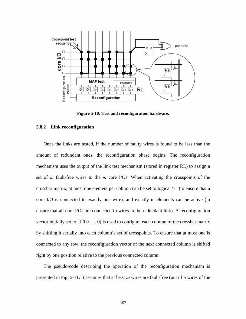
107
Figure 5-10: Test and reconfiguration hardware.
5.8.2 Link reconfiguration
Once the links are tested, if the number of faulty wires is found to be less than the
amount of redundant ones, the reconfiguration phase begins. The reconfiguration
mechanism uses the output of the link test mechanism (stored in register RL) to assign a
set of m fault-free wires to the m core I/Os. When activating the crosspoints of the
crossbar matrix, at most one element per column can be set to logical ‘1’ (to ensure that a
core I/O is connected to exactly one wire), and exactly m elements can be active (to
ensure that all core I/Os are connected to wires in the redundant link). A reconfiguration
vector initially set to [1 0 0 … 0] is used to configure each column of the crossbar matrix
by shifting it serially into each column’s set of crosspoints. To ensure that at most one is
connected to any row, the reconfiguration vector of the next connected column is shifted
right by one position relative to the previous connected column.
The pseudo-code describing the operation of the reconfiguration mechanism is
presented in Fig. 5-11. It assumes that at least m wires are fault-free (out of n wires of the

108
redundant link).
Figure 5-11: Link reconfiguration algorithm.
For each fault-free wire, the reconfiguration vector is constructed by rotating right the
reconfiguration vector of the previous fault-free wire, and then shifted into each column
of the crosspoint matrix. Faulty or unused wires are invalidated by shifting in an all-0
vector on the corresponding column of the crossbar. This ensures that at most one core
I/O is connected to each redundant global wire.
So far, via failure was considered as the predominant yield loss mechanism for global
interconnects. Using active devices for implementing the link test and reconfiguration
hardware adds a potential source of yield loss due to the non-zero probability of failure of
these devices. This effect must be accounted for when estimating the yield of the
interconnect. Conversely, when calculating the number of spares required for achieving a
certain target yield, this additional source of yield loss must be considered as well. We
define the effective interconnect yield Yeff as the interconnect yield achievable in presence
of non-zero probability of failure of test and reconfiguration circuitry. Therefore, the
probability of failure of a single line of interconnect Pline in Eq. (5.2) must be adjusted
accordingly.
-- crosspoint matrix reconfiguration-- initializek = 0; -- column indexl = 0; -- row indexrec_vector = [1000…0]while l < m -- not all rows have been connected
while RL(k) = 0 -- wire k is defectiveinvalidate(k); -- do not use column kk=k+1; -- advance to next wire
end while;column(k) = rec_vector; -- reconfigure column krec_vector = ror (rec_vector); -- rotate right and set the next
--reconfiguration vector l++; -- advance to the next row
end while;

109
As depicted in Fig. 5-2, both ends of each line of the fault-tolerant inter-core links are
connected to the core’s inputs/outputs by a pass-transistor. The probability of failure
PoFT of this transistor can be estimated knowing the killer defect density k [14] for the
manufacturing process under consideration, and the area of the device AT:
T TPoF k A (5.8)
Therefore, Eq. (5.2) must be rewritten to take into account the probability of failure of the
two pass transistors as:
22
1,1
1 1l
line T i ii
P PoF PoF via
(5.9)
Similarly, the effective yield Yeff of an inter-core link must account for the potential yield
loss of the crosspoint matrix elements and test/reconfiguration mechanism. Using again
the killer defect density k and the area AFT of the circuitry used to implement and
reconfigure the fault-tolerant links, the effective yield of a link can be express as:
eff FT m of nY k A P (5.10)
where Pm of n is the yield of the link without considering the yield loss due to fault-tolerant
circuitry, as calculated in Eq. (5.4). In the expression of effective yield Yeff in Eq. (5.10)
we use the adjusted value of Pline corresponding to Eq. (5.9).
The test and reconfiguration sequences can be run at start-up only, both at start-up
and run-time, or during idle periods in which there is no traffic on the particular link. The
amount of time required to run the test/reconfiguration procedures is an important figure
of merit since it expresses how fast the system can be operational after start-up, or how
long the individual links undergoing test/reconfiguration will be unavailable during
run-time. In Section 5.8.3, a more detailed analysis and estimation of these figures of

110
merit is provided, in addition to other cost parameters such as wire complexity and area
overhead associated with the hardware implementation of fault-tolerant interconnects.
5.8.3 Yield, performance and cost analysis
We applied the method developed in this work to sets of global interconnects of
different widths, representative for the cases of massive multi-core communication
fabrics. We considered the case of a 65 nm technology with 12 metal layers and defect
distributions as projected by the ITRS 2006 roadmaps.
Figure 5-12: Physical link width (n) for different values of logic link width (m = 32, 64,128 bits) and target effective yield (Yeff).
Fig. 5-12 plots the total number of wires (including the redundant ones), n, that need
to be routed in order to provide 90%, 99%, and 99.9% effective interconnect yield
respectively, for global link widths (m) of 32, 64, and 128 bits and probability of
defect-free global interconnect line Pline ranging between 0.9 and 1.
The total number of wires n, of the global link, in the above example, was determined
assuming the global interconnects are laid out starting on source/drain contacts, through

111
intermediate metal layers to the upper metal layers and back. As mentioned above, we
use a 65 nm CMOS technology, with a typical defect density of 0.025defects/cm2
obtained from [14].
Table 5-1: Effective yield improvement vs interconnect complexity
Interconnectwidth (m)
Targetinterconnect
effectiveyield Yeff
[%]
Number ofcrosspoints
Interconnecteffective
yieldimprovement
[%]90 25 3.999 58 7.68
99.9 74 8.390 82 11.199 248 15.716
99.9 279 16.190 112 16.999 302 25.832
99.9 725 26.790 285 36.499 573 45.364
99.9 2224 46.590 1192 61.399 5429 70.3128
99.9 10984 71.2
Table 5-1 shows the relative interconnect effective yield improvement (the fourth
column in the table) for a probability of defect-free line Pline = 0.99 and the cost to
achieve it in terms of number of crossbar crosspoints (third column) for different target
interconnect yields and link widths.
As shown in Table 5-1, the yield of NoC interconnects can be significantly improved
by using our technique. It is, however, extremely important to estimate carefully the
target effective yield and characterize the manufacturing process accurately, since
demanding a high yield or underestimating the individual Pline for global interconnects

112
can increase dramatically the size of the fault tolerant crossbars and, implicitly, the
silicon area and metal lines required. For example, if a 99% effective yield is targeted for
a 64-bit wide global link, we need to provide a 573-crosspoint sparse crossbar at each end
of the link; if, instead, a 99.9% yield is aimed for, the number of required crosspoints is
2224. That translates to an approximately 4X increase in silicon area for an interconnect
yield improvement of only 0.9%.
The area overhead of the combined test and reconfiguration mechanisms is presented
in Fig. 5-13, for different crossbar sizes and degrees of redundancy. Note that the amount
of circuitry required for implementing the test and reconfiguration mechanisms is
relatively small. The overhead corresponding to the programmable crosspoints, each
consisting of a pass transistor and a memory cell is reported separately in Table 5-1. Each
crossbar matrix constructed as described in Section 5.5 has a number of ( 1)n n m
such crosspoints.
Area overhead (test and reconfiguration)
0
50
100
150
200
250
300
8 16 32 64 128
crossbar size
25% 50% 75% 100%
Figure 5-13: Area overhead for different crossbar sizes and degrees of redundancy.
Table 5-2 presents the time overhead of test and reconfiguration mechanisms, in

113
clock cycles. These values are important for systems that are required to have a short
start-up time, or, in the case in which the test/reconfiguration mechanism is executed
during the regular operation, for systems that must achieve high availability.
In Table 5-2, TC represents the crossbar test time, and is proportional to the logical
crossbar size (m) and the degree of redundancy (expressed in percentage in Table 5-2).
TL denotes the physical link test time, and is governed by the number of physical wires
that must be realized for each logical link, for achieving a target yield. TR is the link
reconfiguration time, and denotes the amount of time required to shift-in the
reconfiguration vectors for each crossbar. The sum of TC, TL and TR is denoted by
and indicates the total amount of time required to set-up a fault-tolerant link between two
cores of a NoC, either at start-up on during its operation.
Table 5-2: Test and reconfiguration time overhead
25% redundancy 50% redundancy 75% redundancy 100% redundancy
Cro
ssb
ar s
ize
TC TL TR TC TL TR TC TL TR TC TL TR
8 59 60 40 159 119 72 96 287 179 84 168 431 239 96 240 575
16 199 120 140 459 399 144 312 855 599 168 532 1299 799 192 800 1791
32 719 240 480 1439 1439 288 1104 2831 2159 336 1904 4399 2879 384 2880 6143
64 2719 480 1760 4959 3439 576 2592 6607 8159 672 7168 15999 10879 768 10880 22527
128 10559 960 6720 18239 21119 1152 15936 38207 31679 1344 27776 60799 42239 1536 42240 86015
Depending on the link width and the amount of redundancy required by the interconnect
yield target, the fault-tolerant communication links will not be available for transporting
data during their respective test and reconfiguration procedures, for an amount of time
corresponding to the columns labeled “” in Table 5-2.

114
5.9 Summary
In this chapter, a structured method is presented for building defect tolerant NoC
interconnects that takes into account the manufacturing process characteristics in terms of
via failure probability and, in turn, generates interconnects with the desired target yield.
The mechanism that selects and reconfigures the communication links is based on
balanced sparse crossbars, and uses a minimum number of crosspoints to connect the set
of defect-free wires at the core interface. The method also ensures that all valid
interconnect configuration have identical capacitive load, which guarantees the
invariance of timing characteristics of different possible configurations. With the method
described in this chapter, a relative interconnect yield improvement can be obtained in the
range of 3.9% for an 8-bit logic link width to 71.2% for a 128-bit logic link width. An
important advantage of this technique is that it can be easily automated and implemented
in NoC/SoC design tools.
We expect the solution proposed here to become more relevant with the emergence of
nanometer-scale VLSI processes, where high defect rates and device failures will be
serious manufacturing limitations.
115
Chapter 6
6 Conclusions
6.1 Summary of contributions
In this dissertation, an integrated solution for testing and yield-tuning of network-on-
chip (NoC) interconnect infrastructures is presented. A method for testing the NoC fabric
(switches and links) is proposed, that employs the transport of test data progressively
through the NoC, reusing the fault-free NoC elements to deliver test vectors to the NoC
elements under test. Two types of test data transport are proposed. The first is based on a
unicast transport, where test data is directed to each element under test on a single path,
and exactly one NoC component is tested at a time. The second type uses a multicast
transport method, where multiple NoC components are tested concurrently, by delivering
test data simultaneously on multiple paths constructed from fault-free components. The
yield-tuning method that complements the test solution addresses the potential yield loss
in NoC systems due to interconnect defects, and is based on the use of reconfigurable
crossbars and redundant links. A technique is proposed for distributing the crossbar
crosspoints such that all the possible link configurations are characterized by closely
matched signal propagation delays. The benefit of this technique lies in its ability to
provide consistent performance in presence of interconnect defects, with effectively no
delay penalty compared to the fault-free case.
The test procedure of this solution was shown to be faster than previously proposed
methods for NoC test, effectively reducing the test cost and consequently the total cost of
NoC-based chips. Experiments on NoC infrastructure of various sizes and topologies

116
show that the proposed test method can improve the test time with up to 34X when
compared to current solutions. The fault tolerance technique presented here is able to
significantly improve the yield of NoC links, in a range from 3% to 71% for the case of
logical link widths of 8-bit to 128-bit in our experiments.
6.2 Limitations
In this subsection, we enumerate certain limitations and provide views as to how
these limitations can be overcome. One of the aspects that were not addressed in this
dissertation is the power overhead. The test method developed in Chapter 3 is very time-
efficient because it can deliver a large quantity of test data in a short time to the NoC
components across the chip. This comes at a cost of increased power dissipation, which,
potentially, can be a problem depending on the power budget for the design. The solution
is to include the power dissipation as an additional component of the test cost function,
and limit the injection of new test data packets when the maximum power dissipation is
about to be exceeded. Similarly for the fault-tolerant mechanism presented in Chapter 5,
there is a certain amount of power that the extra circuitry (crosspoint elements, test and
reconfiguration hardware) will dissipate through mechanisms such as switching (during
test and reconfiguration phases), and leakage during normal operation. This leakage
power should be included in the overall chip power.
The test solution presented in Chapter 3 is targeted to the NoC infrastructure only.
The main reason behind this approach is that a common trend in industry is to design
NoCs as IP cores, which are generally delivered together with the associated test method.
However, if the testing of the NoC infrastructure is integrated with testing of the
functional cores of the NoC-based chip, there is a possibility to use the concepts in

117
Chapter 3 to deliver test data concurrently to NoC components and functional cores, and
reduce the overall test time of the chip in a more significant manner. We believe that, in
practice, this is not a very likely situation, especially when the NoC is developed as an IP
core and provided to the final user together with its test method.
Another limitation of the fault-tolerant mechanism in Chapter 5 is the significant
increase of link delay when the degree of redundancy increases. This, in turn, implies a
significant defect rate, which will have serious repercussions on the operation of the NoC
functional cores. Therefore, the target yield may not be achievable when a design
constraint is applied to the link delay.
Finally, some form of quantitative estimation of the “amount” of fault-tolerance most
appropriate for each layer of the NoC communication protocol, and the effect of
interaction between FT mechanisms at different layers, would be extremely useful for
designers looking for the best FT solution for NoC-based chips.
6.3 Future work
The high level of concurrency and parallelism in on-chip networks/multi-processor
systems-on-chip is at the same time an opportunity and a challenge. The opportunity is
provided by the great flexibility of these systems in terms of applications (software) that
can be used to manage different aspects of their operation: power management, yield
tuning, and fault-tolerance. These aspects become increasingly challenging with the shift
toward nanoelectronics, which demands a paradigm change best described as “designing
reliable systems with unreliable components” [97]. A few research directions can be
pursued as direct developments of the contributions presented in this dissertation, as
follows:

118
Application-level fault-tolerance for multi-processor systems-on-chip. In the past
few years, fault-tolerance of multi-core chips was addressed mainly through hardware
redundancy or error correction mechanisms. The increased level of faults associated with
nano-scale device sizes demands new approaches for dealing with transient and
permanent faults. There may be a great opportunity to exploit the distributed computing
capabilities of these systems for achieving fault tolerance. The challenge is to integrate
fault-tolerant solutions at application level through software-based micro-agents that
monitor the operation of the system periodically, and restore it to error-free state upon
detection of malfunctions. This would allow a higher degree of flexibility for designers of
fault-tolerant systems-on-chip. Traditionally, hardware-intensive voting mechanisms
based on component replication are used to achieve fault-tolerance at system level.
Complementing the hardware redundancy with state restoration makes possible a more
refined tuning of fault-tolerant capabilities of a MP-SOC depending on the operating
conditions and expected failure rate.
Fault-tolerant crossbar structures for nanoelectronics. Reconfigurable crossbar
arrays are increasingly being proposed as the basic building structure for nanoelectronic
systems [98]. The main challenge in manufacturing commercially viable nanoelectronic
chips is the high defect rate – estimated in the order of 10% or more [99]. This can be
compensated for by adding a certain amount of redundancy to the crossbar structures, and
using reconfiguration techniques to avoid the faulty components. Implicitly, the
performance of such structures is heavily influenced by the degree of redundancy and the
particular reconfiguration mechanism employed. Initial studies have shown that the speed
of reconfigurable crossbar-based structures can vary widely for different instances of the

119
same fault-tolerant array [100]. To account for this variation, designers must take the
conservative approach and report the worst-case performance with the goal of developing
reconfiguration methods for nanoelectronic crossbar arrays that will yield near-optimal,
closely-matched performance for all functional instances, with improved overall speed
and tight parameters variation.
Nanoelectronics is expected to play an important role in providing solutions to
surmount obstacles imposed physical limitations of CMOS electronics. Nanoelectronics
imposes significant quantitative constraints resulting in qualitative modifications to the
design process; among them are an increase in fabric size, density and fault rates which
result in (1) increased emphasis on parallelism, (2) short-range communication, (3)
regular nano-scale interconnects, and (4) offline and online repair of faulty structures.
A fundamental challenge in constructing nanoelectronics-based systems is the high
unreliability of nanoelectronic devices which manifests mainly in two forms. First,
manufacturing defects increase significantly, due to the defect prone fabrication process
through bottom-up self-assembly. The defect rates of nanoelectronic systems are
projected to be orders of magnitude higher than those of current CMOS systems [99].
Second, a high variance in the fault rate at run-time and a clustered behavior of faults are
expected. These are essentially caused by the nanoscale size of the devices as well as the
low operating voltage, which result in extremely high sensitivity to environmental
influences, such as temperature, cosmic radiation and background noise.
The emerging challenges of nanoelectronics require a re-evaluation of the
components and methods typically employed in creating designs. Questions of paramount
importance are related to (1) mapping design descriptions to regular nanofabrics with

120
massive defect rates; (2) realizing defect tolerant designs in the presence of significant
defect occurrence rates and limited test access; (3) development of efficient, systematic
fault tolerance techniques for faults with dynamic spatial and temporal distributions; (4)
ensuring reliability without sacrificing performance.
Due to the difference in complexity at the various system hierarchical levels,
appropriate fault tolerance schemes vary. Building large systems using nanoelectronic
fabrics must include fault-tolerance as one of the primary constraints, similar to
performance, power, area and testability. Moreover, fault-tolerance must be seamlessly
integrated in the design flow starting from physical design and going up to application
design and specification. For instance, an interconnect routing tool should be able to take
into account the possible fault set that can manifest for the particular technology used (e.g.
carbon nanotubes, quantum dots, nano-scale CMOS, or hybrid) and achieve a target yield
in a transparent fashion, without the explicit intervention of the designer. At higher levels
- such as that of application - compilers should be capable to insert automatically micro-
agents for fault management, enabling self-healing by repairing failed components or
restoring the system to fault-free state.
Integrating fault-tolerance into the nanoelectronic system design flow requires an
intimate understanding of fault sources, nature, spatial-temporal distribution, and effects
at different levels from device behaviour to application. Having this knowledge, it is
possible to exploit the particular characteristic of nanoelectronic fabrics, such as
reconfigurability, multiple-valued logic, and high density, for integrating fault-tolerance
into digital nanoelectronics design flow.

121
In summary, the semiconductor industry is rapidly advancing towards nanoscale
domain, driven by continuous miniaturization and need for computing power. The
immediate benefit of integrating fault-tolerance in the design flow for nanoelectronics is
the possibility of a rapid transition from research phase to volume production, enabling
the use of nanoelectronic systems in key areas such as biomedical sciences,
communications, multimedia; ultimately, facilitating developments that are leading us to
the ubiquitous information society.

122
7 Appendices
7.1 Appendix 1: Proof of Correctness for Algorithms 1 and 2
The search sequence that Algorithms 1 and 2 presented in Chapter 3 implement is
based on Dijkstra’s shortest path search algorithm, which is guaranteed to find the
shortest distance between any two vertices in a graph.
Given a graph G(V,E), where V is the set of vertices and E is the set of edges.
Each edge e in E is labeled with its weight w(e) which corresponds to the “length” of that
edge. In the original Dijkstra algorithm, the weights are static and remain constant as long
as the search sequence is executed. In the modified search sequence, the weights are
initialized with a set of values corresponding to the TTPE (test time per element). The
search starts by selecting the edge with minimum weight (minimum TTPE) and adding it
to the set of elements on the shortest path. Before the next minimum-weight element is
selected, the weight of the current element is modified from the value corresponding to
its test time to the value corresponding to the time needed by a test packet to traverse the
NoC element placed in the normal mode of operation. For a link, this corresponds to the
links latency, while for a switch, this is the number of cycles required to transfer a data
packet from an input port to an output port.

123
(a) (b)Figure A1: Shortest path search with dynamical weight updating.
For instance, in Fig. A1(a), assume that the current search path is (v7, v8, v5) and the
current value of the test cost function is F. The next element to be added to the search
path is the edge v5-v6 with weight 4 corresponding to its test time. The edge is added to
the search path which becomes (v7, v8, v5, v6) and the test cost function is updated to its
new value, F+4. In the next step of the search sequence, the test cost function is updated
to its new value F+4+2 = F+6, then edge v6-v3 is added to the search path. The test cost
function becomes F+6+4 = F+10, and then the weight of edge v6-v3 is updated to
F+10+2. At this moment, a minimum length path was found from v7 to v3, and the
algorithm advances to a new pair of vertices.
In the general case, let Pk = (v1, vi, …, vj, vk) be the shortest path from v1 to vk.
Then Pj = (v1, vi, …,vj) must be a shortest path from v1 to vj, otherwise Pk would not be
as short as possible. Also, Pj must be shorter than Pk (assuming all edges have positive
weights).
Let w(j,k) be the weight of the edge between vertices vj and vk as initialized at the
beginning of the algorithm (corresponding to the test time per element TTPE), and
v1 v2 v3
v4 v5 v6
v7 v8 v9
v10 v11 v12
2 5
5 4
2 2
1 2
2
3
3
6
1
4
4
5
2
v1 v2 v3
v4 v5 v6
v7 v8 v9
v10 v11 v12
2 5
5 2
2 2
1 2
2
3
3
6
1
4
4
5
2

124
w’(j,k) the new value of the weight of the (j,k) edge (corresponding to the latency of the
NoC element) that gets updated after edge (j,k) is added to the search path. Since w(j,k)
reflects the test time, and w’(j,k) reflects the latency, the following inequality is true:
w’(j,k) < w(j,k), (vj, vk) E.
If Fk , Fj are the values of the test cost function corresponding to paths Pk, Fj,
respectively, then Fj < Fk. Moreover, Fk is calculated as:
Fk = Fj + w(j,k)
and then updated as:
F’(k) = F(k) + w’(j,k)
Since w’(j,k) < w(j,k) (vj, vk) E, then F’(k) is the minimum possible value of the test
cost function, which proves that the modified shortest path algorithm returns the test path
with the minimum associated test cost.
The main difference between Algorithms 1 and 2, and Dijkstra’s algorithm, is the
manner in which the cost function is updated., Therefore, the order of complexity of
Algorithms 1 and 2 is similar to the one of the original Dijkstra algorithm, i.e., O(N),
where N is the total number of NoC components to be tested (links and switches).

125
7.2 Appendix 2: Algorithm for balancing fault-tolerant sparse
crossbars
Given a (n,m) fat-and-slim sparse crossbar with a AG adjacency matrix
1 0 0 . 0 1 1 1 1 . 1
0 1 0 . 0 1 1 1 1 . 1
0 0 1 . 0 1 1 1 1 . 1
. . . . . . . . 1 . 1
0 0 0 0 1 1 1 1 1 . 1
GA
= Sm|Fm,n-m
the balancing algorithm that matches the fanin+fanout sums corresponding to each of the
elements of AG matrix is described below:
1. Re-arrange the adjacency matrix as
AG = Fmx|Umx(-1)|Bmx(n--2-2)|Lmx(-1), where:
Fmx is a matrix with all elements equal to ‘1’;
Umx(-1) is an upper triangular matrix;
Bmx(n--2-2) is a banded matrix;
Lmx(-1) is a lower triangular matrix;
Let and be [91]:

126
- 1 3, if
2
( 1) ( 1) ( 1) 3, if 0.5, and
2
( 1) ( 1) ( 1) 3, if 0.5, and
2
n m m m n
n
n m m n m m n m m mn
n n n
n m m n m m n m m mn
n n n
;
1n m
where represents an estimation of the average number of ‘1’ per column of matrix
AG, and represents the number columns of matrix F.
F U B L
1 1 . 1 1 1 1 0 . 0 0
1 1 . 1 0 1 1 1 . 0 0
1 1 . 1 0 0 1 1 . . 0
. . . . . . . . . 1 0
1 1 . 1 0 0 0 0 0 1 1
GA
2. Let ‘1’s be assigned to each column in matrix B. Then the number of ‘1’s left in
the F, U and L matrices is (+2-2)( -1), and the number of ‘1’s left unassigned
is
= (n-m+1)m-*n-(+2-2)
The total number of ‘1’s in the AG matrix is greater than or equal to *n:
(n-m+1)m-*n 0,
therefore -(+2-2)

127
Case i): 0
Then the average number of ‘1’s in AG is in the [,+1] interval. Therefore, the
matrix can be balanced by transferring ‘1’s from the columns of the F matrix to the
columns of U and L matrices so that each column has either or +1 ‘1’s, using the
column exchange operation described in Section 5.7.
Case ii): 0
Then the average number of ‘1’s in each column of AG is more than +1. In this case,
a number of1m
columns in F can be balanced with the U and L matrices
such that each balanced column has +1 ‘1’s.
Since
0 (n-m-1)m-*n n,
and
= (n-m-1)m-*n-(+2-2)
then
n-(+2-2).

128
Therefore, the remaining ‘1’s in the unbalanced columns of matrix F can be
distributed to the columns of B, each having at most one additional ‘1’, using the column
exchange operation described in Section 5.7.
Proof of convergence
We prove the convergence of the balancing algorithm by contradiction. Assume that
the balancing algorithm does not converge, that is, the balancing operation ends by
leaving a column that has ‘1’s and another that has +2 ’1’s. Then, a ‘1’ can be moved
from the column with +2 ‘1’s to the column with ’1’s, hence balancing the two
columns. Since the existence of the balanced crossbar is guaranteed, it follows that the
initial assumption is false, and hence the balancing operation converges to a solution.

129
References
[1] G. Sohi, “Single-Chip Multiprocessors: The Next Wave of Computer ArchitectureInnovation”, The 37th Annual IEEE/ACM International Symposium onMicroarchitecture, Dec. 2004.
[2] I. O’Connor, B. Courtois, K. Chakrabarty, M. Hampton, “Heterogeneous Systemson Chip and Systems in Package”, Design, Automation & Test in EuropeConference & Exhibition, 2007.
[3] AMD Fusion Microprocessor Family, http://www.amd.com/us-en/assets/content_type/DownloadableAssets/AMD_Technology_Analyst_Day_News_Summary_FINAL.pdf
[4] W. J. Dally, B. Towles, “Route Packets, Not Wires: On-Chip InterconnectionNetworks”, Proceedings of DAC, Las Vegas, Nevada, USA, June 18-22, 2001, pp:683-689.
[5] J. Owens, W. J. Dally, R. Ho, D. N. Jayashima, S. W. Keckler, L-S. Peh, “ResearchChallenges for On-Chip Interconnection Networks”, IEEE Micro, vol. 27, no. 5, pp.96-108, Sept/Oct, 2007.
[6] T. Ye, L. Benini and G. De Micheli, “Packetization and Routing Analysis of On-chip Multiprocessor Networks”, Journal of System Architecture, Vol. 50, Issues2-3,February 2004, pp: 81-104.
[7] P. Magarshack, P. Paulin, “System-on-chip beyond the nanometer wall”,Proceedings of DAC, Anaheim, 2003, pp: 419-424.
[8] A. Kumar, P. Kundu, A. Singh, L.-S. Peh, N. Jha. “A 4.6Tbits/s 3.6GHz Single-cycle NoC Router with a Novel Switch Allocator in 65nm CMOS”, InternationalConference on Computer Design (ICCD), October, 2007.
[9] E. Nigussie, T. Lehtonen, S. Tuuna, J. Plosila, J. Isoaho, “ High-Performance LongNoC Link Using Delay-Insensitive Current-Mode Signaling“, VLSI Design, Vol.2007 (2007), Article ID 46514.
[10] J. Chan, S. Parameswaran, “NoCOUT: NoC topology generation with mixedpacket-switched and point-to-point networks”, ASP-DAC, 2008, pp: 265-270.
[11] R. Saleh, S. Wilton, S. Mirabbasi, A. Hu, M. Greenstreet, P. Pande, C. Grecu, A.Ivanov, “System on Chip: Reuse and Integration ”, Proceedings of the IEEE, Vol.94, Issue 6, June 2006, pp. 1050-1069.
[12] Y. Li (editor), Microelectronic Applications of Chemical Mechanical Planarization,Wiley, 2007.
[13] Y. Zorian, D. Gizopoulos, C. Vandenberg, P. Magarshack, “Guest editors'introduction: design for yield and reliability”, IEEE Design & Test of Computers,May-June 2004, Vol. 21, Issue: 3, pp. 177–182.
[14] International Technology Roadmap for Semiconductors, 2006 update,http://www.itrs.net/Links/2006Update/2006UpdateFinal.htm
[15] S. Shoukourian, V. Vardanian, Y. Zorian, “SoC yield optimization via anembedded-memory test and repair infrastructure”, IEEE Design & Test ofComputers, May-June 2004, Vol. 21 , Issue: 3, pp. 200 – 207.

130
[16] P. Pande, C. Grecu, A. Ivanov, R. Saleh, G. De Micheli, “Design, Syndissertationand Test of Networks on Chip”, IEEE Design and Test of Computers, Vol. 22, No.5, 2005, pp: 404-413.
[17] D.A. Hodges, H.G. Jackson, R.A. Saleh, Analysis and Design of Digital IntegratedCircuits: In Deep Submicron Technology, McGraw-Hill, 3rd edition, 2003.
[18] L. Benini, G. De Micheli, “Networks on Chip: A New Paradigm for Systems onChip Design”, International Conference on Design and Test in Europe DATE, Paris2002, pp. 418-419.
[19] Intel Teraflops Research Chip, http://techresearch.intel.com/articles/Tera-Scale/1449.htm
[20] A. Jantsch and Hannu Tenhunen, editors, Networks on Chip, Kluwer AcademicPublishers, 2003.
[21] International Standards Organization, Open Systems Interconnection (OSI)Standard 35.100, www.iso.org.
[22] Y. Zorian, E. J. Marinissen, S. Dey, “Testing Embedded-Core-Based SystemChips”, IEEE Computer Vol. 32, Issue 6, pp: 52-60, 1999.
[23] E. J. Marinissen, R. Arendsen, G. Bos, H. Dingemanse, M. Lousberg, C. Wouters,“A Structured and Scalable Mechanism for Test Access to Embedded ReusableCores”, Proceedings of ITC 1998, pp: 284-293.
[24] E. Cota, Luigi Caro, Flavio Wagner, Marcelo Lubaszewski, “Power aware NoCReuse on the Testing of Core-Based Systems”, Proceedings of ITC 2003, pp: 612-621.
[25] C. Liu, V. Iyengar, J. Shi and E. Cota, “Power-Aware Test Scheduling in Network-on-Chip Using Variable-Rate On-Chip Clocking”, IEEE VLSI Test Symposium,pp: 349-354, 2005.
[26] C. Liu, Z. Link, D. K. Pradhan, “Reuse-based Test Access and Integrated TestScheduling for Network-on-Chip”, Proceedings of Design, Automation and Test inEurope, 2006. DATE '06, pp: 303 – 308.
[27] B. Vermeulen, J. Dielissen, K. Goossens, C. Ciordas, “Bringing CommunicationsNetworks on a Chip: Test and Verification Implications”, IEEE CommunicationsMagazine, Volume 41, Issue 9, Sept. 2003, pp: 74-81.
[28] M. Nahvi, A. Ivanov, “Indirect Test Architecture for SoC Testing”, IEEETransactions on Computer-Aided Design of Integrated Circuits and Systems,Volume 23, Issue 7, July 2004, pp: 1128-1142.
[29] J. Raik, R. Ubar, V. Govind, “Test Configurations for Diagnosing Faulty Links inNoC Switches”, Proceedings of the 12th IEEE European Test Symposium, 2007,pp: 29-34.
[30] A. M. Amory, E. Briao, E. Cota, M. Lubaszewski, F. G. Moraes, “A Scalable TestStrategy for Network-on-chip Routers”,Proceedings of The IEEE International TestConference, 2005, ITC 2005, pp: 591-599.
[31] M. L. Bushnell and V. D. Agrawal, Essentials of Electronic Testing for Digital,Memory and Mixed-Signal VLSI Circuits, Boston: Springer, 2005.
[32] M. Cuviello, S. Dey, X. Bai, Y. Zhao, “Fault Modeling and Simulation forCrosstalk in System-on-Chip Interconnects”, Proceedings of the IEEE/ACMInternational Conference on Computer-Aided Design, San Jose, CA, Nov. 1999,pp: 297-303.

131
[33] P. P. Pande, C. Grecu, M. Jones, A. Ivanov, R. Saleh, "Performance Evaluation andDesign Trade-offs for MP-SoC Interconnect Architectures", IEEE Transactions onComputers, Volume 54, Issue 8, August 2005, pp: 1025-1040.
[34] J. Duato, S. Yalamanchili, L. Ni, Interconnection Networks – An EngineeringApproach, Morgan Kaufmann, 2002.
[35] I. Saastamoinen, M. Alho, J. Nurmi, “Buffer Implementation for Proteo Network-on-chip”, Proceedings of the 2003 International Symposium on Circuits andSystems, 2003. ISCAS '03, Vol: 2, pp: II-113- II-116.
[36] H. Wang L.-S. Peh, S. Malik, “Power-driven Design of Router Microarchitecturesin On-chip Networks”, Proceedings of the 36th Annual IEEE/ACM InternationalSymposium on Microarchitecture, 2003. MICRO-36, pp: 105- 116.
[37] A.J. Van de Goor, I. Schanstra, Y. Zorian, “Functional test for shifting-type FIFOs”,Proceedings of European Design and Test Conference 1995, March 1995, pp. 133-138.
[38] C. E. Leiserson, “Fat-trees: Universal Networks for Hardware-EfficientSupercomputing”, IEEE Transactions on Computers, October 1985, Volume 34,Issue 10, pp: 892 – 901.
[39] A.O. Balkan, Q. Gang, V. Uzi, “A Mesh-of-Trees Interconnection Network forSingle-Chip Parallel Processing”, International Conference on Application-specificSystems, Architectures and Processors, ASAP, Sept. 2006, pp: 73 – 80.
[40] M. Millberg, E. Nilsson, R. Thid, S. Kumar, and A. Jantsch “The Nostrumbackbone - a communication protocol stack for networks on chip”, Proceedings ofthe IEEE VLSI Design Conference, Mumbai, India, January 2004, pp: 693- 696.
[41] Intel IXP2400 datasheet, http://www.intel.com/design/network/products/npfamily/ixp2400.htm
[42] J. Liu, L-R. Zheng, H. Tenhunen, “Interconnect intellectual property for network-on-chip (NoC)”, Journal of Systems Architecture: the EUROMICRO Journal,Volume 50 , Issue 2-3 (February 2004), pp: 65 – 79.
[43] A. Radulescu, J. Dielissen, K. Goossens, E. Rijpkema, P. Wielage, “An Efficienton-chip Network Interface Offering Guaranteed Services, Shared-memoryAbstraction, and Flexible Network configuration”, Proceedings of IEEE DATE2004, vol. 2, pp: 878-883.
[44] P. P. Pande, C. Grecu, A. Ivanov, R. Saleh, "Switch-Based InterconnectArchitecture for Future Systems on Chip", Proceedings of SPIE, VLSI Circuits andSystems, Vol. 5117, pp: 228-237, 2003.
[45] C-M. Chiang, L. Ni, “Multi-address Encoding for Multicast”, Proceedings of theFirst International Workshop on Parallel Computer Routing and Communication,pp: 146-160, 1994.
[46] Z. Lu, B. Yin, A. Jantsch, “Connection-oriented multicasting in wormhole-switchednetworks on chip”, IEEE Computer Society Annual Symposium on Emerging VLSITechnologies and Architectures, 2006.
[47] E. Bolotin, Z. Guz, I. Cidon, R. Ginosar, A. Kolodny, “The Power of Priority: NoCBased Distributed Cache Coherency”, The First International Symposium onNetworks-on-Chip, 2007. NOCS 2007, pp: 117 – 126.
[48] T. H. Cormen, C. E. Leiserson, R. L. Rivest, and C. Stein. Introduction toAlgorithms, Second Edition, MIT Press and McGraw-Hill, 2001.

132
[49] Y. Zorian, E. J. Marinissen, S. Dey, “Testing Embedded-core-based System Chips”,IEEE Computer, Volume 32, Issue 6, June 1999, pp. 52-60.
[50] M. Nahvi, A. Ivanov, “An embedded autonomous scan-based results analyzer(EARA) for SoC cores”, Proceedings of the 21st IEEE VLSI Test Symposium, 2003,pp: 293-298.
[51] A. DeHon, “Compact, Multilayer Layout for Butterfly Fat-tree”, Proceedings of the12th Annual ACM Symposium on Parallel Algorithms and Architectures, 2000, pp:206 – 215.
[52] Synopsys TetraMAX ATPG Methodology Backgrounder,www.synopsys.com/products/test/tetramax_wp.html
[53] IEEE Std 1500 - Standard for Embedded Core Test, online,http://grouper.ieee.org/groups/1500/index.html
[54] C. Grecu, P. Pande, A. Ivanov, R. Saleh, “Timing Analysis of Network on ChipArchitectures for MP-SoC Platforms”, Microelectronics Journal, Elsevier, Vol.36(9), pp: 833-845.
[55] C. Constantinescu, “Trends and challenges in VLSI circuit reliability”, IEEE Micro,July-Aug. 2003, Vol. 23, Issue: 4, pp. 14-19.
[56] D. Bertozzi, L. Benini, G. De Micheli, ‘’Error Control Schemes for On-ChipCommunication Links: The Energy-Reliability Tradeoff ‘’, IEEE Transactions onComputer-Aided Design of Integrated Circuits and Systems, Vol. 24, No. 6, June2005, pp. 818-831.
[57] S. R. Sridhara, and N. R. Shanbhag, “Coding for System-on-Chip Networks: AUnified Framework”, IEEE Transactions on Very Large Scale Integration (TVLSI)Systems, Vol. 13, No. 6, June 2005, pp. 655-667.
[58] M. Lajolo, “Bus guardians: an effective solution for online detection and correctionof faults affecting system-on-chip buses”, IEEE Transactions on VLSI Systems,Vol. 9, Issue: 6, Dec. 2001, pp: 974-982.
[59] D. Bertozzi, L. Benini, G. De Micheli, “Low power error resilient encoding for on-chip data buses”, Proceedings of the Design, Automation and Test in EuropeConference and Exhibition, (DATE), 4-8 March. 2002, pp: 102-109.
[60] J. Kim, D. Park, T. Teocharides, N. Vijaykrishnan, C. R. Das, “A low latencyrouter supporting adaptivity for on-chip interconnects”, Proceedings of the 42nd
DAC, Anaheim, 2005, pp: 559 – 564.[61] T. Dumitras, S. Kerner, and R. Marculescu, “Towards on-chip fault-tolerant
communication”, in Proceedings of ASP-DAC, Jan. 2003. pp: 225-232.[62] M. Pirretti, G. Link, R. R. Brooks, N. Vijaykrishnan, M. Kandemir, M. J. Irwin,
“Fault Tolerant Algorithms for Network-On-Chip Interconnect”, Proceedings ofIEEE ISVLSI 2004, pp: 46-51.
[63] B. Joshi, D. Pradhan, J. Stiffler. "Fault-tolerant computing", Wiley Encyclopedia ofComputer Science and Engineering, January 15, 2008.
[64] S Manolache, P Eles, Z Peng, “Fault and Energy-Aware Communication Mappingwith Guaranteed Latency for Applications Implemented on NoC”, Proceedings ofDAC 2005, pp: 266 – 269.
[65] D. Ferrero, C. Padró, “Connectivity and fault-tolerance of hyperdigraphs”, DiscreteApplied Mathematics 117 (2002), pp: 15-26.

133
[66] P. P. Pande, A. Ganguly, B. Feero, B. Belzer, C. Grecu, “Design of low power andreliable networks on chip through joint crosstalk avoidance and forward errorcorrection coding”, Proceedings of IEEE DFT Symposium, DFT’06, 2006, pp:466-476.
[67] S. Murali, T. Theocharides,. N. Vijaykrishnan, M. J. Irwin, L. Benini, G. DeMicheli, “Analysis of error recovery schemes for networks on chips”, IEEE Design& Test of Computers, Sept.-Oct. 2005, Vol: 22, Issue: 5, pp: 434- 442.
[68] P. D. T. O’Connor, Practical Reliability Engineering, 4th edition, Wiley, June 2002.[69] C. Grecu, A. Ivanov, R. Saleh, E. S. Sogomonyan, P. P. Pande, "On-line fault
detection and location for NoC interconnects," Proceedings of the 12th IEEEInternational On-Line Testing Symposium (IOLTS'06), 2006, pp. 145-150.
[70] L. Benini, G. De Micheli, “Networks on Chips: A New SoC Paradigm”, IEEEComputer, Vol. 35, Issue 1, pp: 70-78, 2002.
[71] M. Zhang, N.R. Shanbhag, “Soft-Error-Rate-Analysis (SERA) Methodology”,IEEE Transactions on Computer-Aided Design of Integrated Circuits and Systems,Volume 25, Issue 10, Oct. 2006 pp: 2140 – 2155.
[72] E. Bolotin, I. Cidon, R. Ginosar and A. Kolodny, ”QNoC: QoS architecture anddesign process for Network on Chip", Special Issue on Networks on Chip, TheJournal of Systems Architecture, December 2003.
[73] G. Masson, “Binomial switching networks for concentration and distribution”,IEEE Transactions on Communications, Sep 1977, Vol. 25, Issue: 9, pp. 873–883.
[74] S. G. Shiva, Advanced Computer Architectures, CRC Press, 2005.[75] B. Wilkinson, “On crossbar switch and multiple bus interconnection networks with
overlapping connectivity”, IEEE Transactions on Computers, Vol. 41, Issue 6, June1992, pp. 738-746.
[76] L. Noordergraaf, R. Zak, “SMP System Interconnect Instrumentation forPerformance Analysis”, Proceedings of the ACM/IEEE Conference onSupercomputing 2002, pp. 53-62.
[77] T. Dumitras, R. Marculescu, “On-chip stochastic communication”, Proceedings ofthe IEEE Design, Automation and Test in Europe Conference, 2003, pp. 0790-10795.
[78] M. Pirretti, G. M. Link, R. R. Brooks, N. Vijaykrishnan, M. T. Kandemir, M. J.Irwin, “Fault tolerant algorithms for network-on-chip interconnect”, Proceedings ofISVLSI 2004, pp. 46-51
[79] H. Zhu, P. P. Pande, C. Grecu, "Performance evaluation of adaptive routingalgorithms for achieving fault tolerance in NoC fabrics," Proceedings of 18th IEEEInternational Conference on Application-specific Systems, Architectures andProcessors, ASAP 2007.
[80] J. Huang, M. B. Tahoori, F. Lombardi, “Fault tolerance of switch blocks and switchblock arrays in FPGA”, IEEE Transactions on Very Large Scale Integration (VLSI)Systems, Vol. 13 , Issue 7, July 2005, pp. 794-807.
[81] J. M. Emmert, S. Baumgart, P. Kataria, A. M. Taylor, C. E. Stroud, M. Abramovici,“On-line fault tolerance for FPGA interconnect with roving STARs”, Proceedingsof the IEEE International Symposium on Defect and Fault-Tolerance in VLSISystems, 2001, pp.445-454.

134
[82] N. Harrison, “A simple via duplication tool for yield enhancement”, IEEEInternational Symposium on Defect and Fault Tolerance in VLSI Systems, 2001, pp.39-47.
[83] K. McCullen, “Redundant via insertion in restricted topology layouts”, Proceedingsof the 8th International Symposium on Quality Electronic Design, (ISQED’07),2007, pp. 821-828.
[84] G. A. Allan, “Targeted layout modification for semiconductor yield/reliabilitymodifications”, IEEE Transactions on Semiconductor Manufacturing, Vol. 17,Issue 4, Nov. 2004 pp. 573 – 581.
[85] G. A. Allan, J. Walton, “Automated redundant via placement for increased yieldand reliability”, Proceedings of SPIE, Vol. 3216, Microelectronics ManufacturingYield, Reliability, and Failure Analysis III, September 1997, pp. 114-125.
[86] G. Xu, L.-D. Huang, D. Z. Pan, M. D. F. Wong, “Redundant-via enhanced mazerouting for yield improvement”, Proceedings of the 2005 ASP-DAC, 2005, pp.1148-1151.
[87] S. Gandemer, B.C. Tremintin, J.-J. Charlot, “Critical area and critical levelscalculation in IC yield modeling”, IEEE Transaction on Electron Devices, Vol. 35,Issue: 2, Feb. 1988, pp. 158-166.
[88] A. Cabrini, D. Cantarelli, P. Cappelletti, R. Casiraghi, A. Maurelli, Marco Pasotti,P.L. Rolandi, G. Torelli, “A test structure for contact and via failure analysis indeep-submicrometer CMOS technologies”, IEEE Transactions on SemiconductorManufacturing, Feb. 2006, Vol. 19, Issue: 1, pp. 57-66.
[89] D.K. de Vries, P.L.C. Simon, “Calibration of open interconnect yield models”,Proceedings of the 18th IEEE International Symposium on Defect and FaultTolerance in VLSI Systems, 2003, pp. 26-33.
[90] M. D. Grammatikakis, D. F. Hsu, M. Kraetzl, Parallel System Interconnections andCommunications, CRC Press, 2000.
[91] W. Guo, A. Y. Oruc, “Regular Sparse Crossbar Concentrators”, IEEE Transactionson Computers, Vol. 47 , Issue 3, March 1998, pp. 363-368.
[92] HSPICE, http://www.synopsys.com/products/mixedsignal/hspice/hspice.html,Synopsys, Inc.
[93] K. Goossens, J. Dielissen, A. Radulescu, “The Aethereal network on chip:concepts, architectures, and implementations”, IEEE Design and Test ofComputers, Sept-Oct 2005, Vol. 22, Issue: 5, pp. 414-421.
[94] C. Grecu, A. Ivanov, R. Saleh, P.P. Pande, “Testing network-on-chipcommunication fabrics”, IEEE Transactions on Computer-Aided Design ofIntegrated Circuits and Systems, Vol. 26, Issue 12, Dec. 2007, pp. 2201 – 2214.
[95] E. Gunduzhan, A. Y. Oruç, “Structure and density of sparse crossbarconcentrators,” DIMACS Series in Discrete Mathematics and Computer Science.Advances in Switching Networks. 1998, Vol. 42. pp. 169-180.
[96] G. Lemieux, D. Lewis, `”Design of Interconnection Networks for ProgrammableLogic”, Kluwer Academic Publishers, 2004.
[97] P. Bose, “Designing reliable systems with unreliable components”, IEEE Micro,Vol. 26, Issue 5, Sept-Oct. 2006, pp. 5-6.

135
[98] G. Snider, P. Kuekes, T. Hogg1 and R. Stanley Williams, “Nanoelectronicarchitectures”, Journal of Applied Physics A: Materials Science & Processing,Volume 80, Number 6, March, 2005, pp: 1183-1195.
[99] R. I. Bahar, D. Hammerstrom, J. Harlow, W. H. Joyner Jr., C. Lau; D. Marculescu,A. Orailoglu; M. Pedram “Architectures for Silicon Nanoelectronics and Beyond”,Computer, Vol. 40, Issue 1, Jan. 2007, pp: 25-33.
[100] A. Schmid, Y. Leblebici, “Regular array of nanometer-scale devices performinglogic operations with fault-tolerance capability”, IEEE Conference onNanotechnology, Munich, 2004, pp: 399-401.
[101] C. Grecu, C. Rusu, A. Ivanov, R. Saleh, L. Anghel, P. P. Pande, “A FlexibleNetwork-on-Chip Simulator for Early Design Space Exploration”, The 1st
Microsystems and Nanoelectronics Research Conference (MNRC 2008), Ottawa,2008.
[102] Advanced Microcontroller Bus Architecture,www.arm.com/products/solutions/AMBAHomePage.html.