Embed Size (px)
Citation preview
SEI TECHNICAL REVIEW · NUMBER 84 · APRIL 2017 · 131
AUTOMOTIVE
1. Introduction
Nowadays more and more car functions are controlled electrically in order to improve environmental perfor-mance, safety, and comfort. This means an increase in the number of electronic control units, which in turn increases the number of sensors and other devices connected to those units, and accordingly the number of circuits in individual units and the number of pins on the connectors. With multiway connectors, a greater force is required to mate the connector (connector mating force) in the process of attaching it to the vehicle, reducing the workability.
Conventionally, when the mating force increased, the connectors were split up or a lever structure was built in the connector to withstand the increased force. However, the installation space allotted to the electronic control units is shrinking to secure the comfort and convenience of the passengers, making these conventional solutions difficult as they require more space.
For this reason, there are increasing demands for the development of plating that reduces the insertion force and friction coefficient of the connector, so that the mating force can be kept low even if the number of pins increases.
Sumitomo Electric Industries, Ltd. has created a connector with an increased number of pins through the development of an original plating technology that lowers the insertion force of terminals, which accounts for the majority of the mating force of connectors.
2. Contact and Wear Mechanism
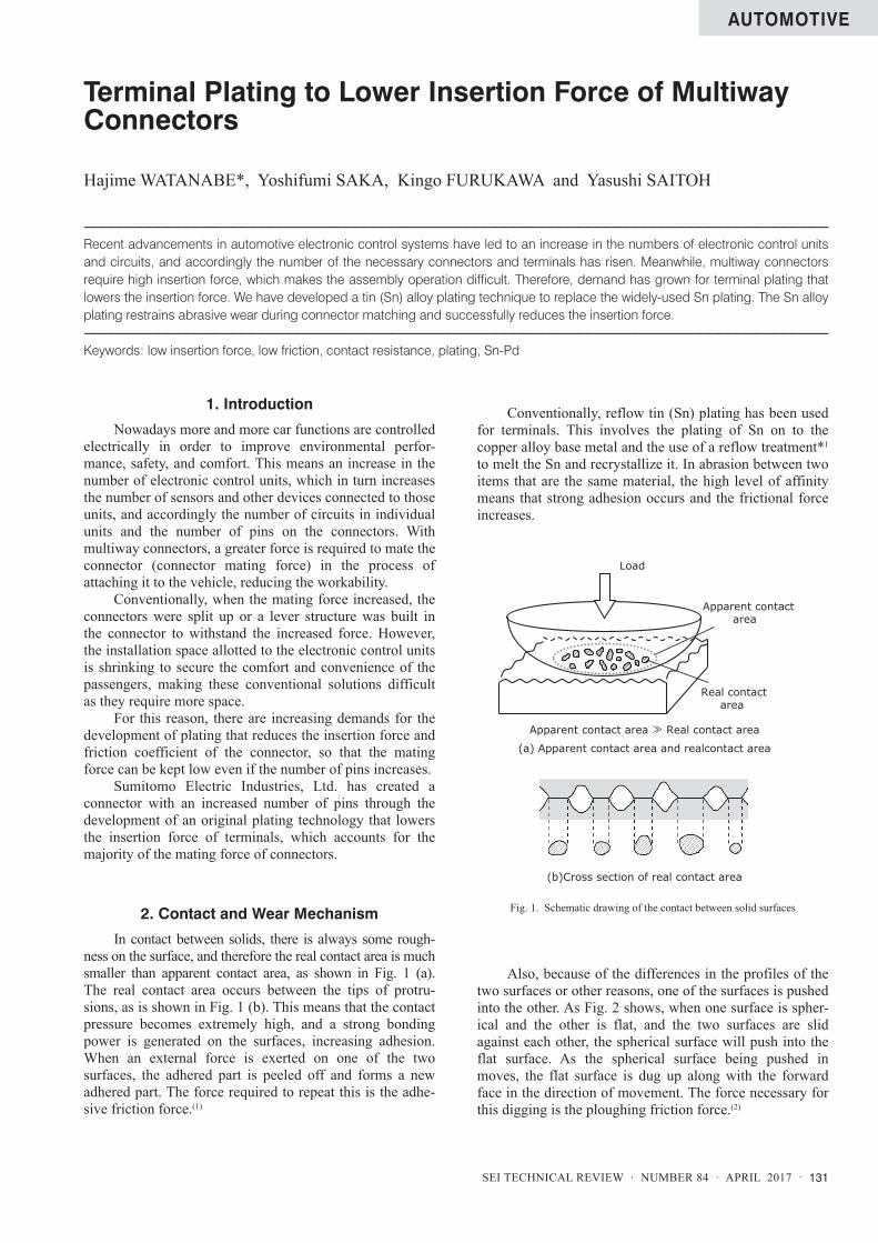
In contact between solids, there is always some rough-ness on the surface, and therefore the real contact area is much smaller than apparent contact area, as shown in Fig. 1 (a). The real contact area occurs between the tips of protru-sions, as is shown in Fig. 1 (b). This means that the contact pressure becomes extremely high, and a strong bonding power is generated on the surfaces, increasing adhesion. When an external force is exerted on one of the two surfaces, the adhered part is peeled off and forms a new adhered part. The force required to repeat this is the adhe-sive friction force.(1)
Conventionally, reflow tin (Sn) plating has been used for terminals. This involves the plating of Sn on to the copper alloy base metal and the use of a reflow treatment*1 to melt the Sn and recrystallize it. In abrasion between two items that are the same material, the high level of affinity means that strong adhesion occurs and the frictional force increases.
Also, because of the differences in the profiles of the two surfaces or other reasons, one of the surfaces is pushed into the other. As Fig. 2 shows, when one surface is spher-ical and the other is flat, and the two surfaces are slid against each other, the spherical surface will push into the flat surface. As the spherical surface being pushed in moves, the flat surface is dug up along with the forward face in the direction of movement. The force necessary for this digging is the ploughing friction force.(2)
Terminal Plating to Lower Insertion Force of Multiway Connectors
Hajime WATANABE*, Yoshifumi SAKA, Kingo FURUKAWA and Yasushi SAITOH
----------------------------------------------------------------------------------------------------------------------------------------------------------------------------------------------------------------------------------------------------------Recent advancements in automotive electronic control systems have led to an increase in the numbers of electronic control units and circuits, and accordingly the number of the necessary connectors and terminals has risen. Meanwhile, multiway connectors require high insertion force, which makes the assembly operation difficult. Therefore, demand has grown for terminal plating that lowers the insertion force. We have developed a tin (Sn) alloy plating technique to replace the widely-used Sn plating. The Sn alloy plating restrains abrasive wear during connector matching and successfully reduces the insertion force.----------------------------------------------------------------------------------------------------------------------------------------------------------------------------------------------------------------------------------------------------------Keywords: low insertion force, low friction, contact resistance, plating, Sn-Pd
Apparent contact area ≫ Real contact area
(a) Apparent contact area and realcontact area
(b)Cross section of real contact area
Real contactarea
Apparent contactarea
Load
Fig. 1. Schematic drawing of the contact between solid surfaces
132 · Terminal Plating to Lower Insertion Force of Multiway Connectors
The adhesive friction and ploughing friction described above also affect the abrasion between the two Sn-plated surfaces when a terminal is inserted. One previous method developed to reduce the insertion force is plating with a thinned Sn layers, such as the 3-layer plating shown in Table 1. By reducing the thickness of the Sn layer, the apparent hardness increases and the ploughing friction and surface deformation decrease. However, the friction coeffi-cient reduction effect is limited to only around 20%.
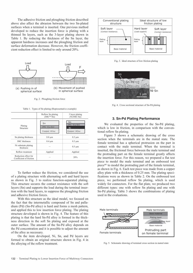
To further reduce the friction, we considered the use of a plating structure with alternating soft and hard layers as shown in Fig. 3 to realize function-separated plating. This structure secures the contact resistance with the soft layers (Sn) and supports the load during the terminal inser-tion with the hard layers, to suppress the ploughing friction and adhesive friction forces.
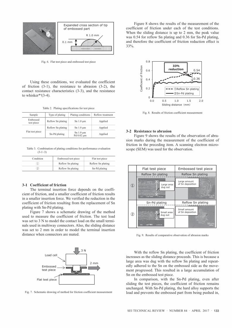
With this structure as the ideal model, we focused on the fact that the intermetallic compound of Sn and palla-dium (Pd) (Sn-Pd alloy) is hard and forms a mesh pattern, and applied this to low insertion force plating. The plating structure developed is shown in Fig. 4. The feature of this plating is that the hard Sn-Pd alloy is formed in the thick-ness direction in the soft Sn plating and exposed at the outer surface. The amount of the Sn-Pd alloy depends on the Pd concentration and it is possible to adjust the amount of the alloy as necessary.
On the item developed, Ni, Sn, and Pd layers are formed to obtain an original structure shown in Fig. 4 in the alloying of the reflow treatment.
3. Sn-Pd Plating Performance
We evaluated the properties of the Sn-Pd plating, which is low in friction, in comparison with the conven-tional reflow Sn plating.
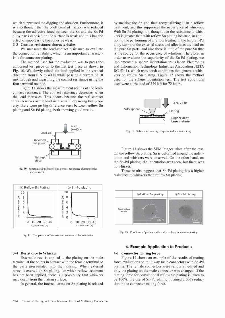
Figure 5 shows a schematic drawing of the cross section when the terminals are in the mated state. The female terminal has a spherical protrusion on the part in contact with the male terminal. When the terminal is inserted, the frictional force between the male terminal and the protruding part on the female terminal greatly affects the insertion force. For this reason, we prepared a flat test piece to model the male terminal and an embossed test piece*3 to model the protruding part of the female terminal, as shown in Fig. 6. Each test piece was made from a copper alloy plate with a thickness of 0.25 mm. The plating speci-fications were as shown in Table 2. On the embossed test piece, we performed reflow Sn plating, which is used widely for connectors. For the flat plate, we produced two different types: one with reflow Sn plating and one with Sn-Pd plating. Table 3 shows the combinations of plating used in the evaluations.
FLoad Load
(a) Pushing in of spherical surface
(b) Movement of pushed in spherical surface
Fig. 2. Ploughing friction force
Table 1. Types of Sn plating (Representative example)
Reflow Sn plating (IMC*2/Sn)
3 layer plating (Ni/IMC/Sn)
Plating Structure
Sn plating thickness 0.8 µm 0.3 µm
IMC thickness 0.4 µm 0.3 µm
Ni substrate plating thickness - 0.5 µm
Reflow treatment Applied Applied
Reduction effect for Coefficient of friction - 20%
Sn
Copper Al loy
IMC(Cu-Sn)
Sn
Copper Al loy
IMC(Cu-Sn)Ni
Conventional platingstructure
Ideal structure of lowfriction plating
Soft layer(Contact resistance)
Hard layer(Load support)
Soft layer(Contact resistance)
Base material Base material
Platinglayer
Platinglayer
Fig. 3. Ideal structure of low friction plating
Fig. 4. Cross sectional structure of Sn-Pd plating
Male terminals
Female terminals
Male terminals
Plating layer
Base material
Protruding parton female terminal
Base material
Plating layer
Fig. 5. Schematic drawing of terminal cross section in mated state
SEI TECHNICAL REVIEW · NUMBER 84 · APRIL 2017 · 133
Using these conditions, we evaluated the coefficient of friction (3-1), the resistance to abrasion (3-2), the contact resistance characteristics (3-3), and the resistance to whisker*4(3-4).
3-1 Coefficient of frictionThe terminal insertion force depends on the coeffi-
cient of friction, and a smaller coefficient of friction results in a smaller insertion force. We verified the reduction in the coefficient of friction resulting from the replacement of Sn plating with Sn-Pd plating.
Figure 7 shows a schematic drawing of the method used to measure the coefficient of friction. The test load was set to 3 N to model the contact load on the small termi-nals used in multiway connectors. Also, the sliding distance was set to 2 mm in order to model the terminal insertion distance when connectors are mated.
Figure 8 shows the results of the measurement of the coefficient of friction under each of the test conditions. When the sliding distance is up to 2 mm, the peak value was 0.54 for reflow Sn plating and 0.36 for Sn-Pd plating, and therefore the coefficient of friction reduction effect is 33%.
3-2 Resistance to abrasionFigure 9 shows the results of the observation of abra-
sion marks during the measurement of the coefficient of friction in the preceding item. A scanning electron micro-scope (SEM) was used for the observation.
With the reflow Sn plating, the coefficient of friction increases as the sliding distance proceeds. This is because a large area was dug with the reflow Sn plating and repeat-edly adhered to the Sn on the embossed side as the move-ment progressed. This resulted in a large accumulation of Sn on the embossed test piece.
In comparison, with the Sn-Pd plating, even after sliding the test pieces, the coefficient of friction remains unchanged. With Sn-Pd plating, the hard alloy supports the load and prevents the embossed part from being pushed in,
0.1 mm
R 1.0 mm
Expanded cross section of tipof embossed part
Fig. 6. Flat test piece and embossed test piece
Table 2. Plating specifications for test piece
Table 3. Combination of plating conditions for performance evaluation (3-1~3)
Sample Type of plating Plating conditions Reflow treatment
Embossed test piece Reflow Sn plating Sn 1.0 μm Applied
Flat test pieceReflow Sn plating Sn 1.0 μm Applied
Sn-Pd plating Sn 1.0 μmPd 0.02 μm Applied
Condition Embossed test piece Flat test piece
① Reflow Sn plating Reflow Sn plating
② Reflow Sn plating Sn-Pd plating
Embossedtest piece
Flat test piece
Load cell
2 mm
3 N
Fig. 7. Schematic drawing of method for friction coefficient measurement
0
0.2
0.4
0.6
0.8
0.0 0.5 1.0 1.5 2.0
Coe
ffic
ient
of fr
ictio
n
Sliding distance(mm)
①Reflow Sn plating
②Sn-Pd plating
0.36
0.5433%
reduction
Fig. 8. Results of friction coefficient measurement
50 μm
50 μm
①
②
Flat test piece Embossed test pieceReflow Sn plating
Sn-Pd plating
Large areadug out
Large amountof Sn deposition
Reflow Sn plating
Reflow Sn plating
Small areadug out
Small amountof Sn deposition
Fig. 9. Results of comparative observation of abrasion marks
134 · Terminal Plating to Lower Insertion Force of Multiway Connectors
which suppressed the digging and abrasion. Furthermore, it is also thought that the coefficient of friction was reduced because the adhesive force between the Sn and the Sn-Pd alloy parts exposed on the surface is weak and this has the effect of suppressing the adhesive wear.3-3 Contact resistance characteristics
We measured the load-contact resistance to evaluate the connection reliability, which is an important character-istic for connector plating.
The method used for the evaluation was to press the embossed test piece on to the flat test piece as shown in Fig. 10. We slowly raised the load applied in the vertical direction from 0 N to 40 N while passing a current of 10 mA through and measuring the contact resistance using the four-terminal method.
Figure 11 shows the measurement results of the load-contact resistance. The contact resistance decreases when the load increases. This occurs because the real contact area increases as the load increases.(3) Regarding this prop-erty, there were no big difference seen between reflow Sn plating and Sn-Pd plating, both showing good results.
3-4 Resistance to WhiskerExternal stress is applied to the plating on the male
terminal at the points in contact with the female terminal or the parts press-mated into the housing. When external stress is exerted on Sn plating, for which reflow treatment has not been applied, there is a possibility that whiskers may occur from the plating surface.
In general, the internal stress on Sn plating is relaxed
by melting the Sn and then recrystallizing it in a reflow treatment, and this suppresses the occurrence of whiskers. With Sn-Pd plating, it is thought that the resistance to whis-kers is greater than with reflow Sn plating because, in addi-tion to the performing of a reflow treatment, the hard Sn-Pd alloy supports the external stress and alleviates the load on the pure Sn parts, and also there is little of the pure Sn that is the source for the occurrence of whiskers. Therefore, in order to evaluate the superiority of the Sn-Pd plating, we implemented a sphere indentation test (Japan Electronics and Information Technology Industries Association JEITA RC-5241), which uses harsh conditions that generate whis-kers on reflow Sn plating. Figure 12 shows the method used for the sphere indentation test. The test conditions used were a test load of 3 N left for 72 hours.
Figure 13 shows the SEM images taken after the test. On the reflow Sn plating, Sn is deformed around the inden-tation and whiskers were observed. On the other hand, on the Sn-Pd plating, the indentation was seen, but there was no whisker.
These results suggest that Sn-Pd plating has a higher resistance to whiskers than reflow Sn plating.
4. Example Application to Products
4-1 Connector mating forceFigure 14 shows an example of the results of mating
force evaluations on multiway male connectors with Sn-Pd plating. The female connectors were reflow Sn-plated and only the plating on the male connector was changed. If the mating force for conventional reflow Sn plating is taken to be 100%, the use of Sn-Pd plating obtained a 33% reduc-tion in the connector mating force.
Embossedtest piece
Flat testpiece
Load cell
Load0→40 N
AV
Fig. 10. Schematic drawing of load-contact resistance characteristics measurement
① Reflow Sn Plating ② Sn-Pd plating
02468
10
0 10 20 30 40
Con
tact
res
ista
nce
(mΩ
)
Contact load (N)
02468
10
0 10 20 30 40
Con
tact
res
ista
nce
(mΩ
)
Contact load (N)
Fig. 11. Comparison of load-contact resistance characteristics
PlatingSUS sphere
3 N, 72 hr
Copper alloybase material
Fig. 12. Schematic drawing of sphere indentation testing
①Reflow Sn plating ②Sn-Pd plating
Observationresults
50μm 50μm
Fig. 13. Condition of plating surface after sphere indentation testing
SEI TECHNICAL REVIEW · NUMBER 84 · APRIL 2017 · 135
4-2 Connector durability performanceWe performed connector durability evaluations
assuming in-vehicle environments. Normally, the connec-tors are mated once during the vehicle assembly. However, the connectors need to be inserted or removed multiple times if a failure or problem occurs. Assuming these condi-tions, we examined whether the contact resistance could be kept low even after inserting and removing a connector ten times. For Sn related plating, with which the intermetallic compound grows over time, we tested the long-term stability. The samples were stored in an air atmosphere at 160°C for 200 hours, which is an extremely harsh condi-tion where the contact resistance of the conventional reflow Sn plating increases.
Figure 15 shows the results of this series of durability tests. The contact resistance remained unchanged even after mating the connector ten times. A rise in the resistance was seen in the high temperature storage test conducted after inserting and removing the connector ten times, but the value was lower than that on reflow Sn plating.
5. Conclusion
In order to respond to the increase in the number of pins on automotive connectors, we have developed Sn-Pd plating with a low friction coefficient. The results are:
(1) A 33% reduction of the coefficient of friction compared with conventional reflow Sn plating for small terminals
(2) A 33% reduction of the connector mating force
when Sn-Pd plating is applied to the male connector
(3) Connection reliability equivalent to or greater than that of conventional reflow Sn plating
(4) Whisker resistance equivalent to or greater than that of conventional reflow Sn plating
This plating technology has been adopted for our male connectors, which have been mass produced since 2016.
Technical Terms*1 Reflow treatment: A treatment which involves heating
after plating in order to melt and recrystallize the metal to relax internal stress in the plating and form an intermetallic compound through thermal diffusion with the underlying metal, so as to secure plating stability.
*2 IMC: InterMetallic Compound: A compound composed of two or more types of metal.
*3 Embossed test piece: A test piece produced by using a mold to form hemispherical protrusions on a metal plate.
*4 Whiskers: Whisker is a metal single crystal that forms on the surface of the plating. Mainly seen in Sn plating.
References(1) H. Hashimoto, Tribology to learn from the basics, Morikita shuppan
Co. Ltd., PP.21,35-36(2) Y. Yamamoto. M. Kaneta, Tribology, Rikougakusha PP.42-43(3) S. Sawada. et al, Prediction of Electrical Contact Resistance of
Tin-Plated and Silver-Plated Terminals, SEI TECHNICAL REVIEW, Vol. 71, PP.37-43
100%
80%
60%
40%
0%0 1 2 3 4 5 6
Stroke(mm)
Mat
ing f
orce
rat
io
Reflow Sn platingSn-Pd plating
20%
33%reduction
0
5
10
15
20
Mating once Insertion andremoval ten times
After hightemperature storage
Cont
act r
esis
tanc
e (m
Ω)
Refolw Sn plating
Sn-Pd plating
◆Plating condition for male terminal
Fig. 14. Example reduction effect for connecter durability evaluations
Fig. 15. Results of connector durability evaluations

136 · Terminal Plating to Lower Insertion Force of Multiway Connectors
Contributors The lead author is indicated by an asterisk (*).
H. WATANABE*• Circuits and Connection R&D Division,
AutoNetworks Technologies, Ltd.
Y. SAKA• Assistant General Manager, Components Group,
Sumitomo Wiring Systems, Ltd.
K. FURUKAWA• Senior Manager, Circuits and Connection R&D
Division, AutoNetworks Technologies, Ltd.
Y. SAITOH• General Manager, Circuits and Connection R&D
Division, AutoNetworks Technologies, Ltd.