Embed Size (px)
Citation preview
ARTICLE INFORMATION
Journal: Applied Physics Letters
Authors: Seungyul Choi, Yongjoo Kwon, and Junghoon Lee*
Title: Electrowetting-Based Measurement of Interfacial Tension
Supplemental Material
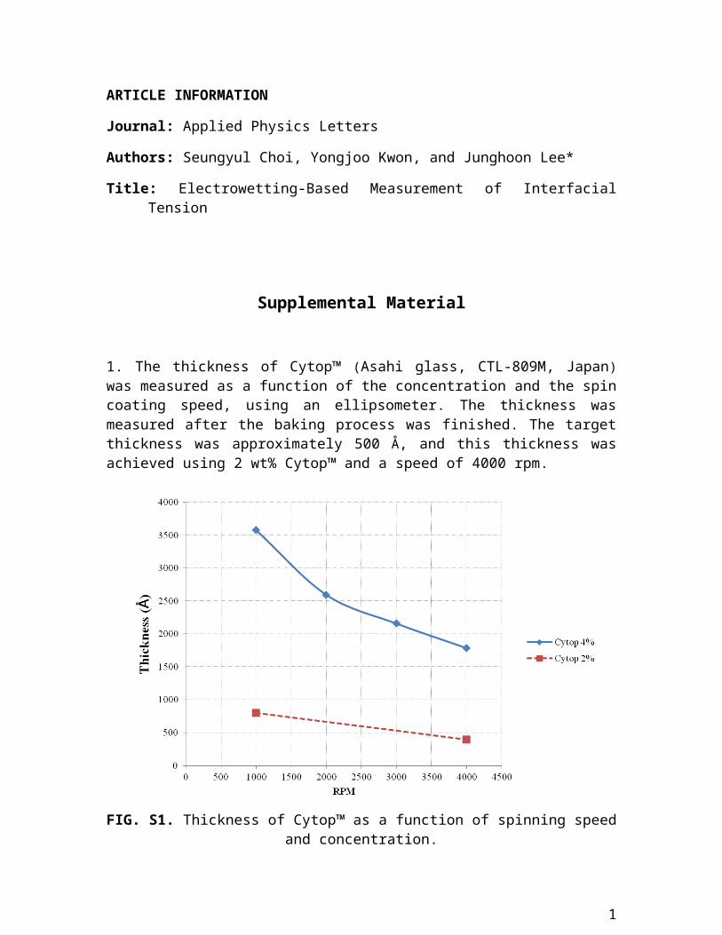
1. The thickness of Cytop™ (Asahi glass, CTL-809M, Japan) was measured as a function of the concentration and the spin coating speed, using an ellipsometer. The thickness was measured after the baking process was finished. The target thickness was approximately 500 Å, and this thickness was achieved using 2 wt% Cytop™ and a speed of 4000 rpm.
FIG. S1. Thickness of Cytop™ as a function of spinning speed and concentration.
2. The process used to fabricate the measurement samples is illustrated in Fig. S2. The first step comprised cleaning the glass wafer with a piranha solution (H2SO4 : H2O2 = 10:1) for 10 min, and subsequently rinsing and drying the wafer. Cr/Au/Cr (200/500/200
1
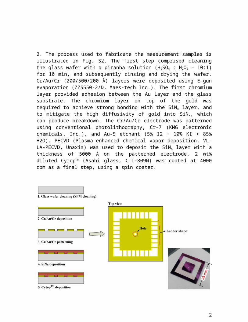
Å) layers were deposited using E-gun evaporation (ZZS550-2/D, Maes-tech Inc.). The first chromium layer provided adhesion between the Au layer and the glass substrate. The chromium layer on top of the gold was required to achieve strong bonding with the SiNx
layer, and to mitigate the high diffusivity of gold into SiNx, which can produce breakdown. The Cr/Au/Cr electrode was patterned using conventional photolithography, Cr-7 (KMG electronic chemicals, Inc.), and Au-5 etchant (5% I2 + 10% KI + 85% H2O). PECVD (Plasma-enhanced chemical vapor deposition, VL-LA-PECVD, Unaxis) was used to deposit the SiNx layer with a thickness of 5000 Å on the patterned electrode. 2 wt% diluted Cytop™ (Asahi glass, CTL-809M) was coated at 4000 rpm as a final step, using a spin coater.
FIG. S2. Schematic illustration of the process used to fabricate the measurement samples, and a photograph of the sample (in the lower right corner). The sample size was 25 mm × 25 mm.
3. Figure. S3 (a) illustrates the process used to fabricate the PDMS reservoir. First, the PDMS base and curing agent were mixed at a ratio of 10:1; here, this mixture is denoted as uncured PDMS. The uncured PDMS was poured into a disposable paper cap, and the curing process was performed at 70°C in an oven. A glass mold to achieve a clear surface with high optical transparency, as shown in Fig. S3 (b). The glass mold was first placed on the cured PDMS, and a self-assembled monolayer (SAM, Trichloro(1H, 1H, 2H, 2H-perfluorooctyl) silane) was deposited, to make it easy to detach the PDMS from mold
2
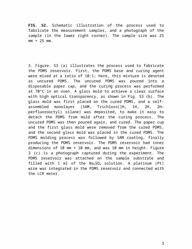
after the curing process. The uncured PDMS was then poured again, and cured. The paper cup and the first glass mold were removed from the cured PDMS, and the second glass mold was placed in the cured PDMS. The PDMS molding process was followed by SAM coating, finally producing the PDMS reservoir. The PDMS reservoir had inner dimensions of 10 mm × 10 mm, and was 10 mm in height. Figure 3 (c) is a photograph captured during the experiment. The PDMS reservoir was attached on the sample substrate and filled with 1 ml of the Na2SO4 solution. A platinum (Pt) wire was integrated in the PDMS reservoir and connected with the LCR meter.
FIG. S3. (a) PDMS reservoir fabrication process. (b) The PDMS reservoir had good optical transparency, because a glass mold with a smooth surface was used. (c) The measurement sample was connected to the LCR meter through the PDMS reservoir’s integrated platinum (Pt) wire and probe tips.
3
4. The optical contact angle was measured via image analysis, using Image J, which is freeware. The low bond axisymmetric drop shape analysis (LB-ADSA) program was used for analysis. It was possible to control the curvature, diameter, and x and y-axis position of the green profile in the image screen using a control panel, as shown in Fig. S4 (a). The droplet images taken from the CCD camera could be magnified and fitted using the green profile curve, and it was possible to define the contact angle in the control panel, as shown in Fig. S4 (b).
FIG. S4. (a) Image screen window (left), and control panel (right) in the LB-ADSA plug-in. (b) Contact angle information could be obtained from the control panel after the green profile was matched with droplet shape.
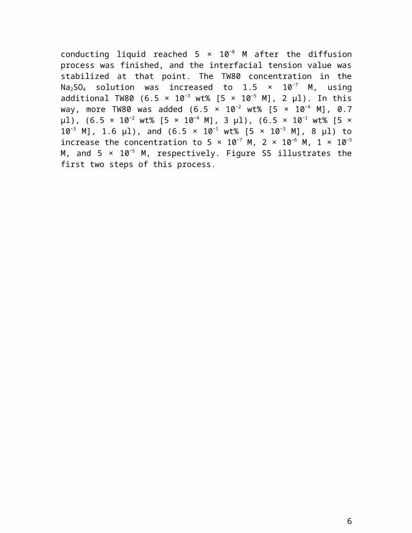
5. First, a certain amount of Tween 80 (TW80; 6.5 × 10⁻³ wt% [5 × 10⁻⁵ M], 1 μl) was placed in the PDMS reservoir, which had previously been filled with 1 ml of an Na2SO4
solution, and the TW80 diffused from the pipette tip, which was placed ~4-5 mm above the substrate. The TW80 concentration in the conducting liquid reached 5 × 10⁻⁸ M after the diffusion process was finished, and the interfacial tension value was stabilized at that point. The TW80 concentration in the Na2SO4 solution was increased to 1.5 × 10⁻⁷ M, using additional TW80 (6.5 × 10⁻³ wt% [5 × 10⁻⁵ M], 2 μl). In this way, more TW80 was added (6.5 × 10⁻² wt% [5 × 10⁻⁴ M], 0.7 μl), (6.5 × 10⁻² wt% [5 × 10⁻⁴ M], 3 μl), (6.5 ×
4

10−1 wt% [5 × 10⁻³ M], 1.6 μl), and (6.5 × 10⁻¹ wt% [5 × 10⁻³ M], 8 μl) to increase the concentration to 5 × 10⁻⁷ M, 2 × 10⁻⁶ M, 1 × 10⁻⁵ M, and 5 × 10⁻⁵ M, respectively. Figure S5 illustrates the first two steps of this process.
FIG. S5. Method used to increase the concentration of Tween 80.
5
6. We observed interfacial data at each concentration. Figure S6 (b) shows magnified views of the graphs in each region, at all six concentrations. The maximum peak-to-peak (pk-pk) noise was calculated in each region. The maximum pk-pk noise was approximately 0.83 mN/m in region 3, and the minimum noise was less than 0.12 mN/m in region 6, where the interfacial tension was low (Fig. S6 (b)). The maximum noise was ±0.42 mN/m, meaning that the resolution of our system was approximately 0.5 mN/m. The smallest difference in interfacial tension values was measured between the concentrations of 5 × 10⁻⁸ M and 1.5 × 10⁻⁷ M. Figure S6 (c) showed that it was possible to measure the changes in interfacial tension that occurred with changes in the concentration; a change in interfacial tension of ~0.9 mN/m was measured from 115 to 185 minute.
FIG. S6. (a) A region was defined at each concentration to determine the noise. (b) The noise in each region. The maximum noise was 0.83 mN/m in region 3, and the minimum was 0.12 mN/m in region 6. (c) A difference of 0.9 mN/m could be detected in the
6
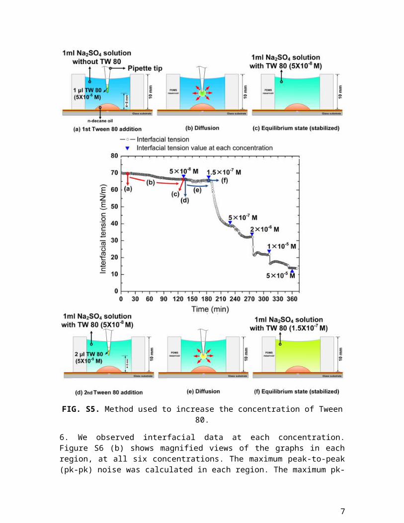
interfacial tension using our system when the concentration was changed from 5 × 10⁻⁸ M to 1.5 × 10⁻⁷ M.
Total No. of Files: 1
File Names: supplementary [Word (.doc)]
File Types: supplementary
Contact Information:
Seungyul Choi#, Junghoon Lee*
Department of Mechanical Engineering, WCU, Seoul National University, Seoul 151-741, Republic of Korea# [email protected]
Yongjoo Kwon
Samsung Advanced Institute of Technology, Samsung electronics, Gyeonggi-do 443-803, Republic of Korea
7