Embed Size (px)
Citation preview
VOL. 2, NO. 3, SEPTEMBER 2018 3501704
Electromagnetic wave sensors
Temperature Effect on the Linearity Performance of a CMOS Image SensorFei Wang1 and Albert J. P. Theuwissen1,2
1Electronic Instrumentation Laboratory, Delft University of Technology, Delft 2628CD, The Netherlands2Harvest Imaging, Bree B-3960, Belgium
Manuscript received May 24, 2018; revised June 29, 2018; accepted July 24, 2018. Date of publication July 31, 2018; date of current version September 3,2018.
Abstract—This article focuses on the effect of the operating temperature of a CMOS image sensor (CIS) on the pixelperformance, especially the linearity behavior. As the temperature increases, the value of the integration capacitor CFD inthe floating diffusion (FD) region increases as well. Moreover, the gain of the in-pixel voltage buffer decreases. These twofactors lead to a reduced value of the conversion gain. Due to an increase in the nonlinear part of the CFD, the linearityof the CIS at a higher temperature will deteriorate. A digital calibration method proposed previously is used to improvethe linearity of the CIS. Measurement results conducted on a prototype image sensor, designed with a 0.18-μm CIStechnology, agree well with an updated analytical model of the CIS and demonstrate an efficient linearity improvement atdifferent temperatures.
Index Terms—Electromagnetic wave sensors, calibration, CMOS image sensor (CIS), linearity, pixel, temperature.
I. INTRODUCTION
Recently, self-driving cars have become a topic of interest. Imagesensors, which are the eyes of an autonomous vehicle, have experi-enced impressive growth [1]. However, this application brings chal-lenges on the image sensor design. An image sensor with high speed,high dynamic range, and an excellent linearity should be able to with-stand harsh temperatures due to complex driving environments, suchas blazing sunlight and large temperature variations.
The imaging performance of the CMOS image sensor (CIS) issignificantly affected by temperature, of which the most notable isthe dark current, which is strongly temperature-dependent [2]. Thetemperature dependence of the full well capacity (FWC) in a CIS hasalso been discussed in [3]. Using an analytical model of the pinnedphotodiode, the authors successfully explained the FWC variationsas a function of temperature and verified the conclusion through atest chip. Based on the bias current’s temperature characteristics ofthe pixel, a temperature compensation method is introduced in [4]to stabilize the output of the CIS against any temperature variations.However, the temperature effect on the linearity performance of theimage sensors has not been well studied.
For image sensors used in autonomous vehicles, linearity is a crucialparameter, especially when the output signal strongly depends on theabsolute measurements of the light input.
In our previous studies, a MATLAB model of the CIS [5] is pro-posed to assist the linearity analysis of the CIS. Furthermore, a digitalcalibration method is presented to improve the linearity performanceof a prototyped CIS [6].
As introduced in [5], the linearity of the CIS is mainly constrained bythe transfer function of the pixel, where the voltage gain of the voltagebuffer and the integration capacitor in the pixel are two determining
Corresponding author: F. Wang (e-mail: [email protected]).Associate Editor: M. Kraft.Digital Object Identifier 10.1109/LSENS.2018.2860990
factors. Both factors have a complicated temperature dependence,which will be disused in the following section.
In this article, the temperature effects on the linearity character-istic of the CIS are analyzed. By adding the temperature model ofthe elements in the proposed model [5], it is possible to perform atemperature-dependent linearity modeling of the CIS. The analysiswas experimentally verified by using two types of pixels, fabricatedwith a 0.18-μm commercial CIS technology. Measurement resultsare in line with the modeling results. The results also demonstratean efficient linearity improvement at different temperatures with theassistance of the calibration method proposed in [6].
II. DEVICE UNDER TEST
The device tested in this article is a rolling-shutter CIS with a128 × 128 pixel array, manufactured through a 0.18-μm CIS process[6]. The pixel array contains several types of pixel designs. A columnamplifier provides a variable gain. Next, a single-slope analog to digitalconverter (ADC) converts the analog signal to a digital output. In thisarticle, two types of pixels are selected to analyze the temperaturecharacteristics. Pixel V1 is a linearity-optimized pixel, which uses anoperational amplifier (OPA) in a closed-loop configuration to reducethe nonlinearity caused by the source follower (SF) in the 4 T pixelV2. Within a limited pixel size, pixel V1 achieved a better linearityat the cost of the fill factor and noise performance. Fig. 1 shows therow select (ROW) and reset transistors (RST) in both pixels, as wellas the SF in pixel V2, which uses a transistor with a low thresholdvoltage Vth.
III. TEMPERATURE ANALYSIS
In a conventional 4 T pixel, the voltage gain of the SF GSF varieswith the pixel output voltage VPIX [5], which leads to a pixel-related
1949-307X C© 2018 IEEE. Personal use is permitted, but republication/redistribution requires IEEE permission.See http://www.ieee.org/publications_standards/publications/rights/index.html for more information.

3501704 VOL. 2, NO. 3, SEPTEMBER 2018
Fig. 1. Schematic of the pixels V1 and V2.
nonlinear error, as follows:
GSF =(
1 + γ
2 · √2ϕF + VP I X
+ λn · √Is√
2 · μ · Cox · (WSF/LSF) · (1 + λn · (VDD − VPIX))
)−1
(1)
where μ is the carrier mobility; Cox is the unit oxide capacitance;λn, WSF, and LSF are the channel-length modulation parameter,width, and length of the nMOS SF, respectively; γ defines thebody-effect parameter; ϕF is the Fermi potential; VDD is the powersupply of the pixel; and Is is the bias current.
More importantly, GSF is temperature-dependent due to the temper-ature effects on the carrier mobility μ, voltage threshold Vth, and biascurrent Is . The variation of the transistor’s mobility μ as a function ofthe temperature is given by
μ(T ) = μ(T0)(T/T0)TCμ (2)
where T is the environment temperature, μ(T0) is the transistor’s mo-bility at room temperature T0, and TCμ is a negative temperature co-efficient (TC) of the mobility, which leads to a decrease in mobilitywith a rise in temperature [7].
Vth can be expressed as follows:
Vth = Vth0 + γ · (√
2ϕF + VSB −√
2ϕF ) (3)
where VSB is the source-bulk voltage, and Vth0 is the threshold voltagevalue of the transistor when VSB is zero. Vth0 has a complex dependenceon the transistor’s size, as reported in [8].
In (3), the Fermi potential ϕF and Vth0 cause a temperature variationin Vth. As given in (4), shown below, ϕF has a complex temperaturedependence; it is directly proportional to temperature. Furthermore, itis related to the value of the material’s intrinsic carrier concentrationni and impurity concentration of the substrate NA. Thus, we have
ϕF = kT/q ln(NA/ni ) (4)
where k is the Boltzmann’s constant and q is the charge of an electron.The intrinsic carrier concentration ni also has a strong temperature
dependence [7], given by
ni ∞T 1.5e−Eg (0)/2kT . (5)
To simplify the analysis, the temperature dependence of Vth is mod-eled with a linear function as follows:
Vth(T ) = Vth(T0) + TCV th(T − T0) (6)
where Vth(T0) is the threshold voltage value at room temperature andthe TC TCV th is related to the size of the transistor. For the transistor
in the bias circuit with a size of 2 μm × 2 μm, the extracted TCV th isaround −1.27 mV/°C.
When the bias transistor is working in saturation, the pixel’s biascurrent Is is given by
IS = 1
2· μ · Cox · W
L· (VGS − Vth)2(1 + λn · VDS) (7)
where W and L are the width and length of the bias transistor, respec-tively, and VGS and VDS are the gate-to-source and the drain-to-sourcevoltages of the transistor, respectively.
IS is related to the values of the carrier mobility μ and Vth,both of which are dependent on temperature. As a result, the vari-ation of the current with temperature is complex. In the pixel cir-cuit, a small bias current Is is chosen such that the decrease of Vth
with temperature is more influential than the decrease in mobilitywith temperature [9]; thus, Is increases with a rise in temperature.The temperature dependence of Is is given by
Is(T ) = Is(T0)(1 + TCI(T − T0)) (8)
where Is(T0) is the current value at room temperature, and the TC TCI
is around 0.25%/°C based on a SPICE simulation.Thus, it is clear that GSF has a complicated temperature dependence.
To simplify the analysis, replacing (1) by a linear function, we get
GSF(T ) = GSF(T0)(1 + TCGSF(T − T0)) (9)
where GSF(T0) is the pixel’s gain at room temperature and the extractedTC TCGSF is −0.029% /°C based on the SPICE simulation.
On the contrary, the gain of the voltage buffer in pixel V1 GOPA
does not vary with VPIX. It is only related to the open-loop gain of theamplifier AOPA as follows:
GOPA = AOPA
1 + AOPA= gm,n R
1 + gm,n R=
(1 + 1
gm,n(ron||rop)
)−1
=(
1 + 2(λn + λp)√
Is√μ · Cox · (Wn/Ln)
)−1
(10)
where R is the equivalent output resistor of the OPA, gm,n is thetransconductance of the input transistors, ron and rop are the outputresistors of the input and load transistors of the OPA, respectively,Wn and Ln denote the size of the input transistors, and λp is thechannel-length modulation parameter of a pMOS transistor.
Similarly, the voltage gain of pixel V1 decreases with a rise intemperature due to the temperature dependence of the carrier mobilityand bias current. It can be simplified as follows:
GOPA(T ) = GOPA(T0)(1 + TCGOPA(T − T0)) (11)
where GOPA(T0) is the pixel’s gain at room temperature and TCGOPA isthe extracted TC, which is around −0.0075% /°C.
In this article, a temperature range of 25–100 °C is chosen due tothe temperature range of the oven used in the measurement. The gaindeviation between the modeled results, from (9) and (11), and theSPICE simulation results, over the whole temperature range, is lessthan 4% for both pixel structures.
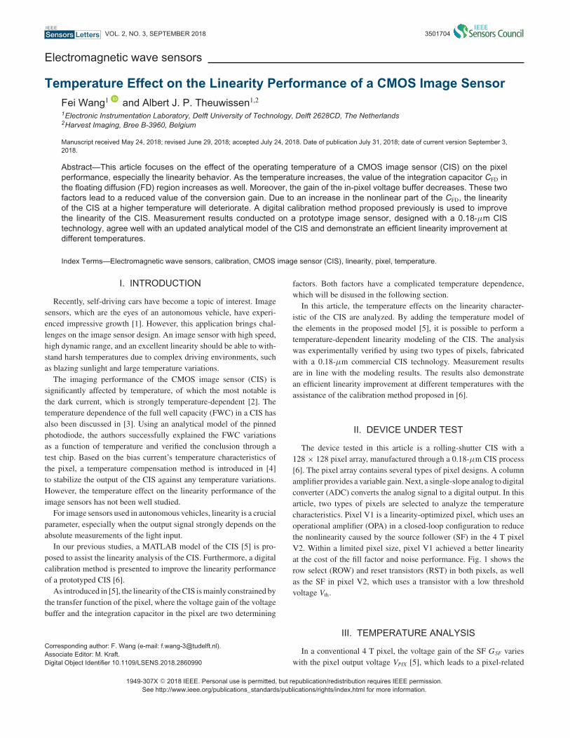
The modeling results of the voltage buffer’s gain in pixels V1 andV2 versus VPIX are shown in Fig. 2. Pixel V1 attains a constant gain.The output voltage of pixel V2 is lower than that of pixel V1 due to theSF’s threshold voltage, when the power supply of the RST transistor
VOL. 2, NO. 3, SEPTEMBER 2018 3501704
Fig. 2. Buffer’s gain versus VPIX. (a) Pixel V1. (b) Pixel V2.
Fig. 3. Cross-sectional view of CFD.
VRST is set as 2.7 V. Furthermore, the gain variation of pixel V1 atdifferent temperatures is also smaller than that of the 4 T pixel V2.
Subsequently, the temperature effects on the capacitor CFD are dis-cussed. The 4 T pixel V2 is used to illustrate the temperature effect,which consists of several types of capacitances [5], [10] from differenttransistors, such as metal capacitance, junction capacitance, overlapcapacitance, and gate–channel capacitance, as shown in Fig. 3.
CM represents the parasitic capacitance of the metal wires.CTX OV, CRST OV, and CSF OV are the overlap capacitances of the TX,RST, and SF transistors, respectively. CSF GB is the equivalent gate–source capacitance to the substrate of the SF, which changes with theSF’s gain due to the Miller effect, and can be expressed as follows:
CSF GB = CSF GS · (1 − GSF) = 2/3 · WSF · LSF · Cox · (1 − GSF).(12)
As presented in [5], CTX OV is related to the channel overlap lengthXdTX and width of the TX transistor WTX. Similarly, CRST OV dependson the channel overlap length XdRST and width of the RST transistorWRST. Thus, we have
CTX OV = XdTX · WTX · Cox; CRST OV = XdRST · WRST · Cox. (13)
CSF OV consists of CSF OV GS and CSF OV GD, which are the gate–source and the gate–drain overlap capacitances of the SF, respectively.CSF OV is related to GSF as follows:
CSF OV = CSF OV GS + CSF OV GD = XdSF · WSF · Cox · (2 − GSF).(14)
From Fig. 3, the junction capacitances of the floating diffusion(FD) consist of the bottom-plate capacitance CFD J and the side-wallcapacitance CFD JSW. CFD J and CFD JSW are directly proportional tothe diffusion area AFD and the perimeter of the FD region PFD. Bothcapacitances are dependent on the voltage value at the FD node VPD.
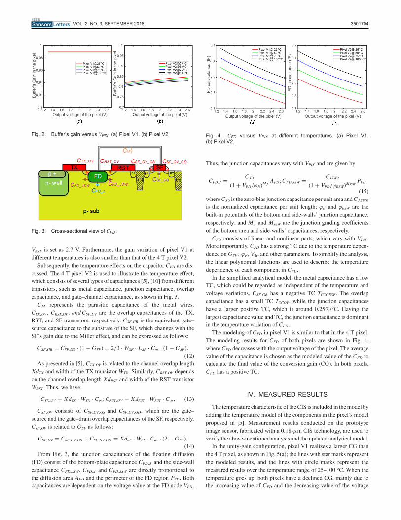
Fig. 4. CFD versus VPIX at different temperatures. (a) Pixel V1.(b) Pixel V2.
Thus, the junction capacitances vary with VPIX and are given by
CFD J = CJ0
(1 + VPD/ϕB)MJAFD; CFD JSW = CJSW0
(1 + VPD/ϕBSW)MJSWPFD
(15)where CJ0 is the zero-bias junction capacitance per unit area and CJ SW 0
is the normalized capacitance per unit length; ϕB and ϕBSW are thebuilt-in potentials of the bottom and side-walls’ junction capacitance,respectively; and MJ and MJSW are the junction grading coefficientsof the bottom area and side-walls’ capacitances, respectively.
CFD consists of linear and nonlinear parts, which vary with VPIX.More importantly, CFD has a strong TC due to the temperature depen-dence on GSF, ϕF , Vth, and other parameters. To simplify the analysis,the linear polynomial functions are used to describe the temperaturedependence of each component in CFD.
In the simplified analytical model, the metal capacitance has a lowTC, which could be regarded as independent of the temperature andvoltage variations. CSF GB has a negative TC TCCGBSF. The overlapcapacitance has a small TC TCCOV, while the junction capacitanceshave a larger positive TC, which is around 0.25%/°C. Having thelargest capacitance value and TC, the junction capacitance is dominantin the temperature variation of CFD.
The modeling of CFD in pixel V1 is similar to that in the 4 T pixel.The modeling results for CFD of both pixels are shown in Fig. 4,where CFD decreases with the output voltage of the pixel. The averagevalue of the capacitance is chosen as the modeled value of the CFD tocalculate the final value of the conversion gain (CG). In both pixels,CFD has a positive TC.
IV. MEASURED RESULTS
The temperature characteristic of the CIS is included in the model byadding the temperature model of the components in the pixel’s modelproposed in [5]. Measurement results conducted on the prototypeimage sensor, fabricated with a 0.18-μm CIS technology, are used toverify the above-mentioned analysis and the updated analytical model.
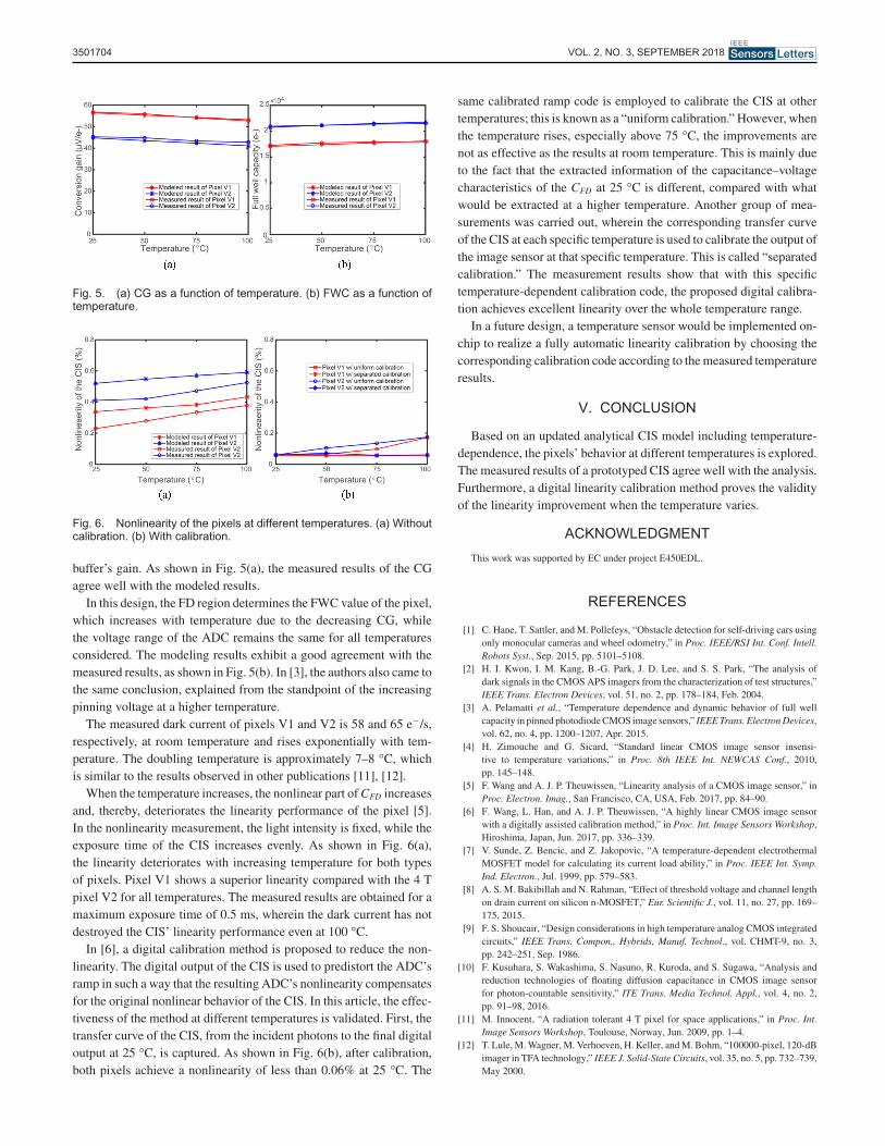
In the unity-gain configuration, pixel V1 realizes a larger CG thanthe 4 T pixel, as shown in Fig. 5(a); the lines with star marks representthe modeled results, and the lines with circle marks represent themeasured results over the temperature range of 25–100 °C. When thetemperature goes up, both pixels have a declined CG, mainly due tothe increasing value of CFD and the decreasing value of the voltage
3501704 VOL. 2, NO. 3, SEPTEMBER 2018
Fig. 5. (a) CG as a function of temperature. (b) FWC as a function oftemperature.
Fig. 6. Nonlinearity of the pixels at different temperatures. (a) Withoutcalibration. (b) With calibration.
buffer’s gain. As shown in Fig. 5(a), the measured results of the CGagree well with the modeled results.
In this design, the FD region determines the FWC value of the pixel,which increases with temperature due to the decreasing CG, whilethe voltage range of the ADC remains the same for all temperaturesconsidered. The modeling results exhibit a good agreement with themeasured results, as shown in Fig. 5(b). In [3], the authors also came tothe same conclusion, explained from the standpoint of the increasingpinning voltage at a higher temperature.
The measured dark current of pixels V1 and V2 is 58 and 65 e−/s,respectively, at room temperature and rises exponentially with tem-perature. The doubling temperature is approximately 7–8 °C, whichis similar to the results observed in other publications [11], [12].
When the temperature increases, the nonlinear part of CFD increasesand, thereby, deteriorates the linearity performance of the pixel [5].In the nonlinearity measurement, the light intensity is fixed, while theexposure time of the CIS increases evenly. As shown in Fig. 6(a),the linearity deteriorates with increasing temperature for both typesof pixels. Pixel V1 shows a superior linearity compared with the 4 Tpixel V2 for all temperatures. The measured results are obtained for amaximum exposure time of 0.5 ms, wherein the dark current has notdestroyed the CIS’ linearity performance even at 100 °C.
In [6], a digital calibration method is proposed to reduce the non-linearity. The digital output of the CIS is used to predistort the ADC’sramp in such a way that the resulting ADC’s nonlinearity compensatesfor the original nonlinear behavior of the CIS. In this article, the effec-tiveness of the method at different temperatures is validated. First, thetransfer curve of the CIS, from the incident photons to the final digitaloutput at 25 °C, is captured. As shown in Fig. 6(b), after calibration,both pixels achieve a nonlinearity of less than 0.06% at 25 °C. The
same calibrated ramp code is employed to calibrate the CIS at othertemperatures; this is known as a “uniform calibration.” However, whenthe temperature rises, especially above 75 °C, the improvements arenot as effective as the results at room temperature. This is mainly dueto the fact that the extracted information of the capacitance–voltagecharacteristics of the CFD at 25 °C is different, compared with whatwould be extracted at a higher temperature. Another group of mea-surements was carried out, wherein the corresponding transfer curveof the CIS at each specific temperature is used to calibrate the output ofthe image sensor at that specific temperature. This is called “separatedcalibration.” The measurement results show that with this specifictemperature-dependent calibration code, the proposed digital calibra-tion achieves excellent linearity over the whole temperature range.
In a future design, a temperature sensor would be implemented on-chip to realize a fully automatic linearity calibration by choosing thecorresponding calibration code according to the measured temperatureresults.
V. CONCLUSION
Based on an updated analytical CIS model including temperature-dependence, the pixels’ behavior at different temperatures is explored.The measured results of a prototyped CIS agree well with the analysis.Furthermore, a digital linearity calibration method proves the validityof the linearity improvement when the temperature varies.
ACKNOWLEDGMENT
This work was supported by EC under project E450EDL.
REFERENCES
[1] C. Hane, T. Sattler, and M. Pollefeys, “Obstacle detection for self-driving cars usingonly monocular cameras and wheel odometry,” in Proc. IEEE/RSJ Int. Conf. Intell.Robots Syst., Sep. 2015, pp. 5101–5108.
[2] H. I. Kwon, I. M. Kang, B.-G. Park, J. D. Lee, and S. S. Park, “The analysis ofdark signals in the CMOS APS imagers from the characterization of test structures,”IEEE Trans. Electron Devices, vol. 51, no. 2, pp. 178–184, Feb. 2004.
[3] A. Pelamatti et al., “Temperature dependence and dynamic behavior of full wellcapacity in pinned photodiode CMOS image sensors,” IEEE Trans. Electron Devices,vol. 62, no. 4, pp. 1200–1207, Apr. 2015.
[4] H. Zimouche and G. Sicard, “Standard linear CMOS image sensor insensi-tive to temperature variations,” in Proc. 8th IEEE Int. NEWCAS Conf., 2010,pp. 145–148.
[5] F. Wang and A. J. P. Theuwissen, “Linearity analysis of a CMOS image sensor,” inProc. Electron. Imag., San Francisco, CA, USA, Feb. 2017, pp. 84–90.
[6] F. Wang, L. Han, and A. J. P. Theuwissen, “A highly linear CMOS image sensorwith a digitally assisted calibration method,” in Proc. Int. Image Sensors Workshop,Hiroshima, Japan, Jun. 2017, pp. 336–339.
[7] V. Sunde, Z. Bencic, and Z. Jakopovic, “A temperature-dependent electrothermalMOSFET model for calculating its current load ability,” in Proc. IEEE Int. Symp.Ind. Electron., Jul. 1999, pp. 579–583.
[8] A. S. M. Bakibillah and N. Rahman, “Effect of threshold voltage and channel lengthon drain current on silicon n-MOSFET,” Eur. Scientific J., vol. 11, no. 27, pp. 169–175, 2015.
[9] F. S. Shoucair, “Design considerations in high temperature analog CMOS integratedcircuits,” IEEE Trans. Compon., Hybrids, Manuf. Technol., vol. CHMT-9, no. 3,pp. 242–251, Sep. 1986.
[10] F. Kusuhara, S. Wakashima, S. Nasuno, R. Kuroda, and S. Sugawa, “Analysis andreduction technologies of floating diffusion capacitance in CMOS image sensorfor photon-countable sensitivity,” ITE Trans. Media Technol. Appl., vol. 4, no. 2,pp. 91–98, 2016.
[11] M. Innocent, “A radiation tolerant 4 T pixel for space applications,” in Proc. Int.Image Sensors Workshop, Toulouse, Norway, Jun. 2009, pp. 1–4.
[12] T. Lule, M. Wagner, M. Verhoeven, H. Keller, and M. Bohm, “100000-pixel, 120-dBimager in TFA technology,” IEEE J. Solid-State Circuits, vol. 35, no. 5, pp. 732–739,May 2000.