Embed Size (px)
Citation preview

1
Tema 12
Transistores.
12.a. El transistor bipolar
12.b. El transistor MOS

Capítulo12.a
El Transistor Bipolar
2

Fundamentos Físicos de la Informática – Curso Académico 2007-2008 Prof. Paula López Martínez
Microelectronic Circuits -
Fifth Edition
Sedra/Smith
3
Figure 5.1 A simplified structure of the npn transistor.
El transistor bipolar de unión, BJT, npn
Fundamentos Físicos de la Informática – Curso Académico 2007-2008 Prof. Paula López Martínez
Microelectronic Circuits -
Fifth Edition
Sedra/Smith
4
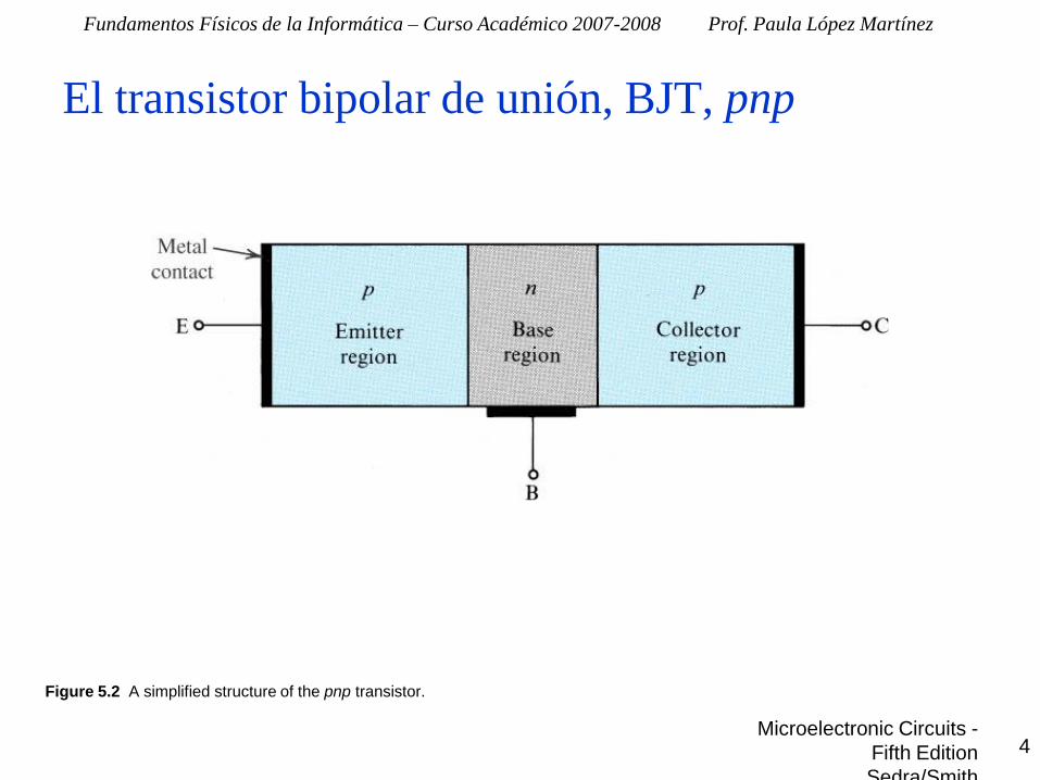
Figure 5.2 A simplified structure of the pnp transistor.
El transistor bipolar de unión, BJT, pnp

Fundamentos Físicos de la Informática – Curso Académico 2007-2008 Prof. Paula López Martínez
Símbolos
5Microelectronic Circuits -
Fifth Edition
Sedra/Smith
5
Figure 5.13 Circuit symbols for BJTs.
Fundamentos Físicos de la Informática – Curso Académico 2007-2008 Prof. Paula López Martínez
Microelectronic Circuits -
Fifth Edition
Sedra/Smith
6
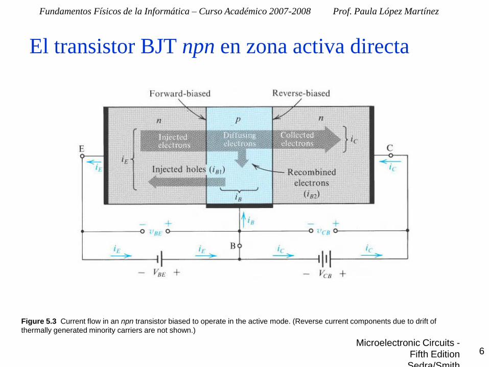
Figure 5.3 Current flow in an npn transistor biased to operate in the active mode. (Reverse current components due to drift of
thermally generated minority carriers are not shown.)
El transistor BJT npn en zona activa directa

Fundamentos Físicos de la Informática – Curso Académico 2007-2008 Prof. Paula López Martínez
Microelectronic Circuits -
Fifth Edition
Sedra/Smith
7
Figure 5.4 Profiles of minority-carrier concentrations in the base and in the emitter of an npn transistor operating in the active mode:
vBE 0 and vCB 0.
Distribución de portadores minoritarios

Fundamentos Físicos de la Informática – Curso Académico 2007-2008 Prof. Paula López Martínez
Corrientes de portadores
8
nae
BC
nd
BEFI
na
BC JJJ
KTqV
nde
BEKT
qVpde
BE
nd
BE
pd
BE
d
EB
BEBE
eJeJJJJ
a
BE
d
BEBE
KTqV
BE
a
BE
d
BEBE
JJJ
eJJJJBE
0
0 1
Proporción de minoritarios que
consigue atravesar la base
nd
BE
pd
BEFI JJ
Flujos de carga proporcionales a la distribución de Maxwell-Boltzmann:
Corriente en la unión BE:
(Corriente diodo directa)
Corriente en la unión CB:
BEFKT
qV
BCCB JeJJCB
10

Fundamentos Físicos de la Informática – Curso Académico 2007-2008 Prof. Paula López Martínez
9
Circuito equivalente en zona activa directa
BEFBCBEFC
BFB
F
FCBEE
CBFEFCCBE
IIII
IIIII
IIIIIII
1
0

Fundamentos Físicos de la Informática – Curso Académico 2007-2008 Prof. Paula López Martínez
Microelectronic Circuits -
Fifth Edition
Sedra/Smith
10
Figure 5.19 (a) Conceptual circuit for measuring the iC –vCE characteristics of the BJT. (b) The iC –vCE characteristics of a practical
BJT.
Curva característica del BJT npn

Fundamentos Físicos de la Informática – Curso Académico 2007-2008 Prof. Paula López Martínez
Polarización en Emisor Común
11

Fundamentos Físicos de la Informática – Curso Académico 2007-2008 Prof. Paula López Martínez
El BJT como amplificador
• Modelo de pequeña señal
12
Fundamentos Físicos de la Informática – Curso Académico 2007-2008 Prof. Paula López Martínez
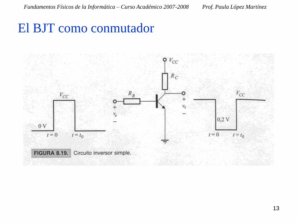
El BJT como conmutador
13

Fundamentos Físicos de la Informática – Curso Académico 2007-2008 Prof. Paula López Martínez
Lógica DTL (Diode-Transistor Logic)
14
Circuito inversor DTL:
Función de transferencia aproximada para el inversor DTL:

Fundamentos Físicos de la Informática – Curso Académico 2007-2008 Prof. Paula López Martínez
Lógica TTL (Transistor-Transistor Logic)
15
Circuito inversor TTL

Fundamentos Físicos de la Informática – Curso Académico 2007-2008 Prof. Paula López Martínez
Circuito inversor TTL con salida en colector
abierto
16
Fundamentos Físicos de la Informática – Curso Académico 2007-2008 Prof. Paula López Martínez
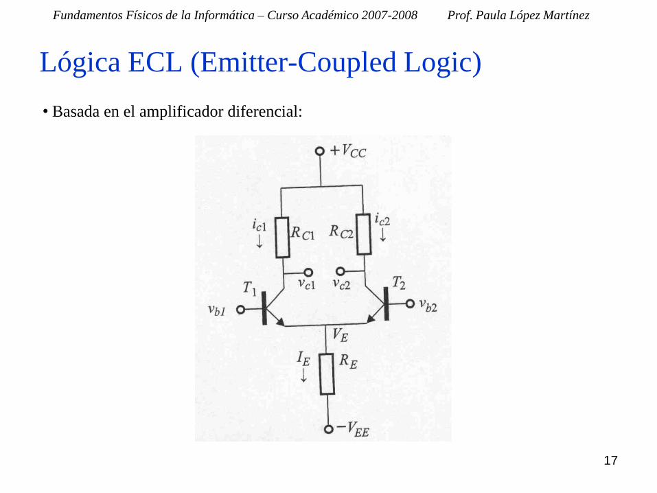
Lógica ECL (Emitter-Coupled Logic)
17
• Basada en el amplificador diferencial:

Capítulo12.b
El Transistor MOS (Metal Oxide
Semiconductor)
18

Fundamentos Físicos de la Informática – Curso Académico 2007-2008 Prof. Paula López Martínez
Microelectronic Circuits -
Fifth Edition
Sedra/Smith
19
Figure 4.1 Physical structure of the enhancement-type NMOS transistor: (a) perspective view; (b) cross-section. Typically L = 0.1 to 3
mm, W = 0.2 to 100 mm, and the thickness of the oxide layer (tox) is in the range of 2 to 50 nm.
Estructura

Fundamentos Físicos de la Informática – Curso Académico 2007-2008 Prof. Paula López Martínez
Microelectronic Circuits -
Fifth Edition
Sedra/Smith
20
Figure 4.9 Cross-section of a CMOS integrated circuit. Note that the PMOS transistor is formed in a separate
n-type region, known as an n well. Another arrangement is also possible in which an n-type body is used and
the n device is formed in a p well. Not shown are the connections made to the p-type body and to the n well; the
latter functions as the body terminal for the p-channel device.
Estructura

Fundamentos Físicos de la Informática – Curso Académico 2007-2008 Prof. Paula López Martínez
Microelectronic Circuits -
Fifth Edition
Sedra/Smith
21
Figure 4.10 (a) Circuit symbol for the n-channel enhancement-type MOSFET. (b) Modified circuit symbol with
an arrowhead on the source terminal to distinguish it from the drain and to indicate device polarity (i.e., n
channel). (c) Simplified circuit symbol to be used when the source is connected to the body or when the effect
of the body on device operation is unimportant.
Símbolo

Fundamentos Físicos de la Informática – Curso Académico 2007-2008 Prof. Paula López Martínez
Microelectronic Circuits -
Fifth Edition
Sedra/Smith
22
Figure 4.2 The enhancement-type NMOS transistor with a positive voltage applied to the gate. An n channel is
induced at the top of the substrate beneath the gate.
Polarización

Fundamentos Físicos de la Informática – Curso Académico 2007-2008 Prof. Paula López Martínez
Microelectronic Circuits -
Fifth Edition
Sedra/Smith
23
Figure 4.3 An NMOS transistor with vGS > Vt and with a small vDS applied. The device acts as a resistance whose
value is determined by vGS. Specifically, the channel conductance is proportional to vGS – Vt’ and thus iD is
proportional to (vGS – Vt) vDS. Note that the depletion region is not shown (for simplicity).
Polarización

Fundamentos Físicos de la Informática – Curso Académico 2007-2008 Prof. Paula López Martínez
Microelectronic Circuits -
Fifth Edition
Sedra/Smith
24
Figure 4.5 Operation of the enhancement NMOS transistor as vDS is increased. The induced channel acquires
a tapered shape, and its resistance increases as vDS is increased. Here, vGS is kept constant at a value > Vt.
Polarización

Fundamentos Físicos de la Informática – Curso Académico 2007-2008 Prof. Paula López Martínez
Microelectronic Circuits -
Fifth Edition
Sedra/Smith
25
Figure 4.6 The drain current iD versus the drain-to-source voltage vDS for an enhancement-type NMOS
transistor operated with vGS > Vt.
Regiones de operación
Fundamentos Físicos de la Informática – Curso Académico 2007-2008 Prof. Paula López Martínez
Microelectronic Circuits -
Fifth Edition
Sedra/Smith
26
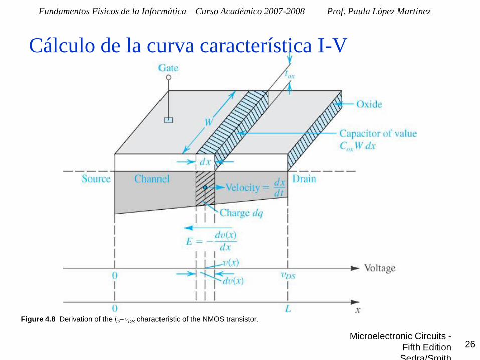
Figure 4.8 Derivation of the iD–vDS characteristic of the NMOS transistor.
Cálculo de la curva característica I-V

Fundamentos Físicos de la Informática – Curso Académico 2007-2008 Prof. Paula López Martínez
Microelectronic Circuits -
Fifth Edition
Sedra/Smith
27
Figure 4.11 (a) An n-channel enhancement-type MOSFET with vGS and vDS applied and with the normal
directions of current flow indicated. (b) The iD–vDS characteristics for a device with k’n (W/L) = 1.0 mA/V2.
Curva característica I-V

Fundamentos Físicos de la Informática – Curso Académico 2007-2008 Prof. Paula López Martínez
Microelectronic Circuits -
Fifth Edition
Sedra/Smith
28
Figure 4.15 Increasing vDS beyond vDSsat causes the channel pinch-off point to move slightly away from the
drain, thus reducing the effective channel length (by DL).
Zona de saturación

Fundamentos Físicos de la Informática – Curso Académico 2007-2008 Prof. Paula López Martínez
Microelectronic Circuits -
Fifth Edition
Sedra/Smith
29
Figure 4.53 The CMOS inverter.
El inversor CMOS

Fundamentos Físicos de la Informática – Curso Académico 2007-2008 Prof. Paula López Martínez
Microelectronic Circuits -
Fifth Edition
Sedra/Smith
30
Figure 4.54 Operation of the CMOS inverter when vI is high: (a) circuit with vI = VDD (logic-1 level, or VOH); (b)
graphical construction to determine the operating point; (c) equivalent circuit.
El inversor CMOS

Fundamentos Físicos de la Informática – Curso Académico 2007-2008 Prof. Paula López Martínez
Microelectronic Circuits -
Fifth Edition
Sedra/Smith
31
Figure 4.55 Operation of the CMOS inverter when vI is low: (a) circuit with vI = 0 V (logic-0 level, or VOL); (b)
graphical construction to determine the operating point; (c) equivalent circuit.
El inversor CMOS

Fundamentos Físicos de la Informática – Curso Académico 2007-2008 Prof. Paula López Martínez
Microelectronic Circuits -
Fifth Edition
Sedra/Smith
32
Figure 4.56 The voltage transfer characteristic of the CMOS inverter.
El inversor CMOS

Fundamentos Físicos de la Informática – Curso Académico 2007-2008 Prof. Paula López Martínez
Microelectronic Circuits -
Fifth Edition
Sedra/Smith
33
Figure 4.57 Dynamic operation of a capacitively loaded CMOS inverter: (a) circuit; (b) input and output
waveforms; (c) trajectory of the operating point as the input goes high and C discharges through QN; (d)
equivalent circuit during the capacitor discharge.
Retardos de propagación
Fundamentos Físicos de la Informática – Curso Académico 2007-2008 Prof. Paula López Martínez
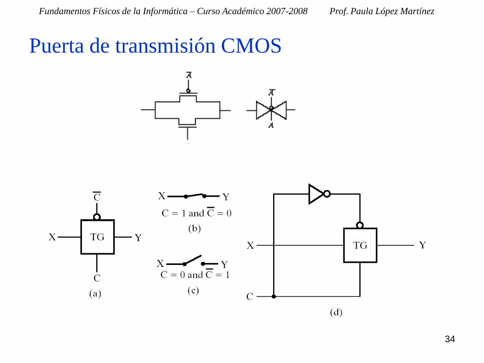
Puerta de transmisión CMOS
34

Fundamentos Físicos de la Informática – Curso Académico 2007-2008 Prof. Paula López Martínez
Puertas NAND y NOR CMOS
35
VDD VDD
VB
VA
VA
VB
Vout
Vout
Figura 7. Puertas NAND (a) y NOR (b) con tecnología CMOS.