Embed Size (px)
Citation preview
TEM and XPS studies of nanocrystals andclusters in nanostructured materials used for
memory storage applications
Annett Thøgersen
Thesis submitted in partial fulfillmentof the requirements for the degree of
Philosophiae Doctor
Department of PhysicsUniversity of Oslo
April 2009
© Annett Thøgersen, 2009 Series of dissertations submitted to the Faculty of Mathematics and Natural Sciences, University of Oslo Nr. 859 ISSN 1501-7710 All rights reserved. No part of this publication may be reproduced or transmitted, in any form or by any means, without permission. Cover: Inger Sandved Anfinsen. Printed in Norway: AiT e-dit AS, Oslo, 2009. Produced in co-operation with Unipub AS. The thesis is produced by Unipub AS merely in connection with the thesis defence. Kindly direct all inquiries regarding the thesis to the copyright holder or the unit which grants the doctorate. Unipub AS is owned by The University Foundation for Student Life (SiO)
Summary
Nanoscaled electronic devices have attracted much attention due to their optical and electronicproperties, especially related to MOS (Metal-Oxide-Semiconductor) devices used for memorystorage applications. Improved electrical properties, longer retention, lower gate voltage andlower power consumption are assumed to be possible when replacing bulk floating gate in flashmemory devices with nanocrystals. Multilayer samples with Si, Ge, Er-oxide, and Pd nanocrys-tals and clusters were studied in detail. The nucleation, distribution, defects, composition, andatomic and electronic structure are important factors to understand in order to improve perfor-mance of memory storage devices. These parameters were studied by high resolution transmis-sion electron microscopy, energy filtered transmission electron microscopy, electron energy lossspectroscopy, X-ray photoelectron spectroscopy, energy dispersive spectroscopy, and secondaryion-mass spectrometry.
iii


Acknowledgments
The past four years have been tough, crazy, and fun. There are many people I wish to thank forsupporting and helping me with my PhD project and generally for keeping me sane.
First of all I want to thank Arne Olsen for supervising me and helping me with my work. Youlured me into electron microscopy, supported me, and challenged me. This I will use in manyyears to come. Spyros Diplas, your knowledge of XPS altered the course of my thesis, pavingthe way for new results. But most of all you inspired me to view data from a different angle.
Furthermore, I wish to thank the administrators at the Department of Physics, SMN, and FUN-MAT@UIO for funding and providing all the means for my project. I am grateful to TerjeFinstad, Bengt Svensson, Jeyanthinath Mayandi, Lasse Vines, Jens Christensen, Martin F. Sund-ing, Anette Gunnæs, Johan Taftø, Ole Bjørn Karlsen, Mesanori Mitome, and Yoshio Bando forsupporting my thesis work.
I also want to thank my friends, especially Bailey, Ingunn, Ingvild, Kanutte, Klaus, and Øysteinfor invigorating discussions, being good friends, and their herculean effort to keep me sane. I amgrateful to my family, especially my parents, for being there for me all these years. I finished myeducation, and all of this would not have been possible without your continuous support.
Finally I want to thank Georg. I love you, you have been my rock, and without you I would belost.
Annett ThogersenApril 2009
v

Preface
This study started in the autumn of 2004 and was funded by FUNMAT@UIO. The main workon this thesis was carried out at the Structure Physics research group at the Institute of Physics,University of Oslo. The PhD work was in cooperation with the Physical Electronics group atMINAlab, where another PhD student made the samples. My supervisors were Arne Olsen,Terje Finstad, and Bengt Svensson.
Part of my work was done during a four months research stay in the autumn of 2006 at theInternational Centre of Young Scientists (ICYS) at the National Institute of Material Science(NIMS) in Tsukuba, Japan. The results from my work there are present in all four papers. Mysupervisors at NIMS were Prof. Yoshio Bando and Dr. Masanori Mitome. The research stay wasfunded by a travel scholarship from FUNMAT@UIO, “Kristine Bonnevie” and SCANDEM.
My main work was to study Si, Ge, Er-oxide, and Pd nanocrystals and clusters in multilayersamples using different transmission electron microscopy and X-ray photoelectron spectroscopytechniques. Papers related to my Ph.D. work and collaborations with other groups that are notincluded in this thesis are presented below.
• J Mayandi, T G Finstad, S Foss, A Thøgersen, U Serincan and R Turan. Luminescencefrom silicon nanoparticles in SiO2: atomic force microscopy and transmission electronmicroscopy studies. Physica Scripta T126, 77 2006
• M. Avice, S. Diplas, A. Thøgersen, J. S. Christensen, U. Grossner, B. G. Svensson, O.Nilsen, H. Fjellvag and J. F. Watts. Rearrangement of the oxide-semiconductor interfacein annealed Al2O3/4H-SiC structures. Applied Physics Letters 91, 052907 2007
• J. Mayandi, T.G. Finstad, S. Foss, A. Thøgersen, U. Serincan, R. Turan. Ion beam syn-thesized luminescent Si nanocrystals embedded in SiO2 films and the role of damage onnucleation during annealing. Surface and Coatings Technology 201, 8482 2007
• J. Mayandi, T.G. Finstad, A. Thøgersen, S. Foss, U. Serincan, R. Turan. Scanning probemeasurements on luminescent Si nanoclusters in SiO2 films. Thin Solid Films 515, 63752007
vii

viii Chapter 0. Preface
• Spyros Diplas, Marc Avice, Annett Thogersen, Jens S. Christensen, Ulrike Grossner, BengtG. Svensson, Ola Nilsen, Helmer Fjellvag, Steve Hinderc and John F.Watts. Interfacialstudies of Al2O3 deposited on 4H-SiC(0001). Surface and Interface Analysis 40, 8222008
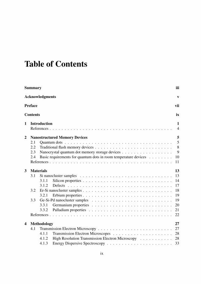
Table of Contents
Summary iii
Acknowledgments v
Preface vii
Contents ix
1 Introduction 1References . . . . . . . . . . . . . . . . . . . . . . . . . . . . . . . . . . . . . . . . . 4
2 Nanostructured Memory Devices 52.1 Quantum dots . . . . . . . . . . . . . . . . . . . . . . . . . . . . . . . . . . . . 52.2 Traditional flash memory devices . . . . . . . . . . . . . . . . . . . . . . . . . . 82.3 Nanocrystal quantum dot memory storage devices . . . . . . . . . . . . . . . . . 92.4 Basic requirements for quantum dots in room temperature devices . . . . . . . . 10References . . . . . . . . . . . . . . . . . . . . . . . . . . . . . . . . . . . . . . . . . 11
3 Materials 133.1 Si nanocluster samples . . . . . . . . . . . . . . . . . . . . . . . . . . . . . . . 13
3.1.1 Silicon properties . . . . . . . . . . . . . . . . . . . . . . . . . . . . . . 143.1.2 Defects . . . . . . . . . . . . . . . . . . . . . . . . . . . . . . . . . . . 17
3.2 Er-Si nanocluster samples . . . . . . . . . . . . . . . . . . . . . . . . . . . . . . 183.2.1 Erbium properties . . . . . . . . . . . . . . . . . . . . . . . . . . . . . . 19
3.3 Ge-Si-Pd nanocluster samples . . . . . . . . . . . . . . . . . . . . . . . . . . . 193.3.1 Germanium properties . . . . . . . . . . . . . . . . . . . . . . . . . . . 203.3.2 Palladium properties . . . . . . . . . . . . . . . . . . . . . . . . . . . . 21
References . . . . . . . . . . . . . . . . . . . . . . . . . . . . . . . . . . . . . . . . . 22
4 Methodology 274.1 Transmission Electron Microscopy . . . . . . . . . . . . . . . . . . . . . . . . . 27
4.1.1 Transmission Electron Microscopes . . . . . . . . . . . . . . . . . . . . 284.1.2 High Resolution Transmission Electron Microscopy . . . . . . . . . . . 284.1.3 Energy Dispersive Spectroscopy . . . . . . . . . . . . . . . . . . . . . . 33
ix
x TABLE OF CONTENTS
4.1.4 Electron Energy Loss Spectroscopy . . . . . . . . . . . . . . . . . . . . 354.1.5 Energy Filtered Transmission Electron Microscopy - Spectral Imaging . . 374.1.6 Scanning Transmission Electron Microscopy . . . . . . . . . . . . . . . 38
4.2 X-ray Photoelectron Spectroscopy . . . . . . . . . . . . . . . . . . . . . . . . . 394.2.1 Photoelectron escape depth . . . . . . . . . . . . . . . . . . . . . . . . . 414.2.2 The binding energy . . . . . . . . . . . . . . . . . . . . . . . . . . . . . 444.2.3 The chemical shift . . . . . . . . . . . . . . . . . . . . . . . . . . . . . 454.2.4 Energy referencing, work function, and the chemical potential . . . . . . 474.2.5 Screening . . . . . . . . . . . . . . . . . . . . . . . . . . . . . . . . . . 504.2.6 Auger parameter . . . . . . . . . . . . . . . . . . . . . . . . . . . . . . 51
4.3 Secondary Ion Mass Spectrometry (SIMS) . . . . . . . . . . . . . . . . . . . . . 53References . . . . . . . . . . . . . . . . . . . . . . . . . . . . . . . . . . . . . . . . . 54
5 Sample preparation 57
6 Overview of papers 61
Paper I:A. Thogersen, J. Mayandi, T. Finstad,J. S. Christensen, M. Mitome, Y. Bando and A. OlsenCharacterization of amorphous and crystalline siliconnanoclusters in an ultrathin silica layer. 68
Paper II:A. Thogersen, S. Diplas J. Mayandi, T. Finstad,M. Mitome, Y. Bando and A. OlsenAn experimental study of charge distribution in crystallineand amorphous Si nanoclusters in thin silica films. 78
Paper III:A. Thogersen, J. Mayandi, T. Finstad,S. Diplas, M. Mitome, Y. Bando and A. OlsenThe formation of Er-oxide nanoclusters in SiO2
thin films with excess Si. 88
Paper IV:A. Thogersen, J. Mayandi, L. Vines, M. F. Sunding, T. Finstad,S. Diplas, M. Mitome, Y. Bando and A. OlsenComposition and electron beam assisted diffusion study of Pd- and Ge- containing nan-oclusters in a SiO2 matrix. 115
List of Abbreviations 117
List of Figures
2.1 A sketch of the energy bands and dielectric function of an atom, a bulk ma-terial and a nanocrystal quantum dot, adapted from Bimberg, Grundmann andLedentsov [5] and Borovitskaya and Shur [6]. . . . . . . . . . . . . . . . . . . . 6
2.2 A sketch of A) a regular flash memory device used today and B) a nanocrystalmemory device. . . . . . . . . . . . . . . . . . . . . . . . . . . . . . . . . . . . 9
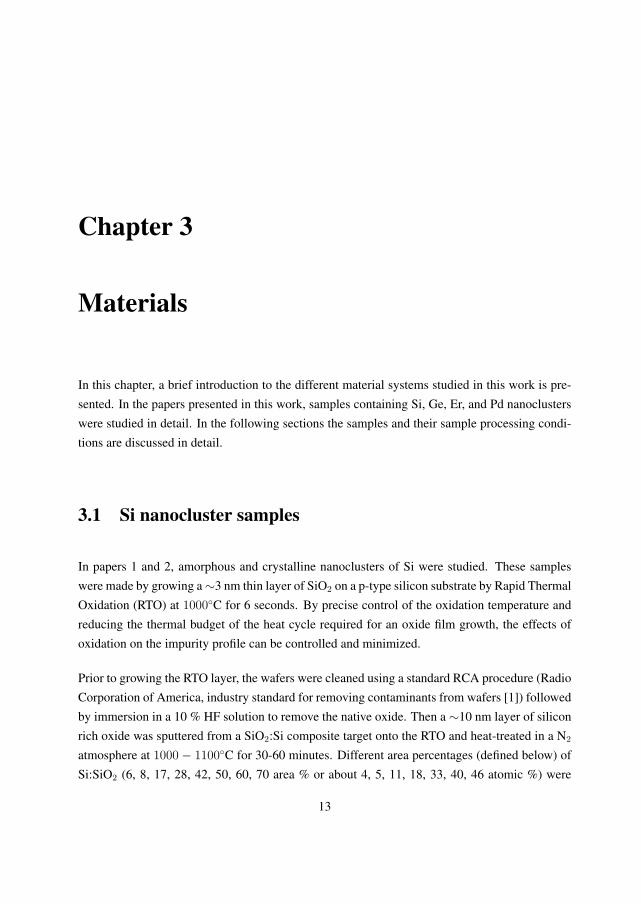
3.1 A sketch of the different samples studied in this thesis. A) The Si samples studiedin paper 1 and 2, B) the Er samples studied in paper 3, and C) the Ge-Pd-Sisamples studied in paper 4. . . . . . . . . . . . . . . . . . . . . . . . . . . . . . 15
3.2 A sketch of the indirect band gap in Si. . . . . . . . . . . . . . . . . . . . . . . . 16
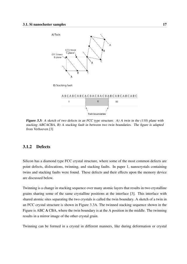
3.3 A sketch of two defects in an FCC type structure. A) A twin in the (110) planewith stacking ABCACBA, B) A stacking fault in between two twin boundaries.The figure is adapted from Verhoeven [3]. . . . . . . . . . . . . . . . . . . . . . 17
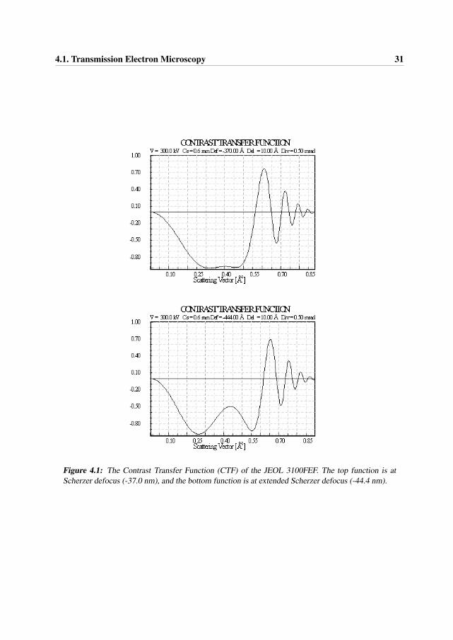
4.1 The Contrast Transfer Function (CTF) of the JEOL 3100FEF. The top function isat Scherzer defocus (-37.0 nm), and the bottom function is at extended Scherzerdefocus (-44.4 nm). . . . . . . . . . . . . . . . . . . . . . . . . . . . . . . . . . 31
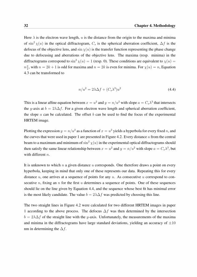
4.2 A plot of n/u2 as a function of u2. The plot was used for finding the focus ofthe HRTEM images in paper 1. The image in the bottom right corner shows adiffractogram of HRTEM image no. 10 and a diffraction pattern from the Si-substrate in the same sample. . . . . . . . . . . . . . . . . . . . . . . . . . . . . 33
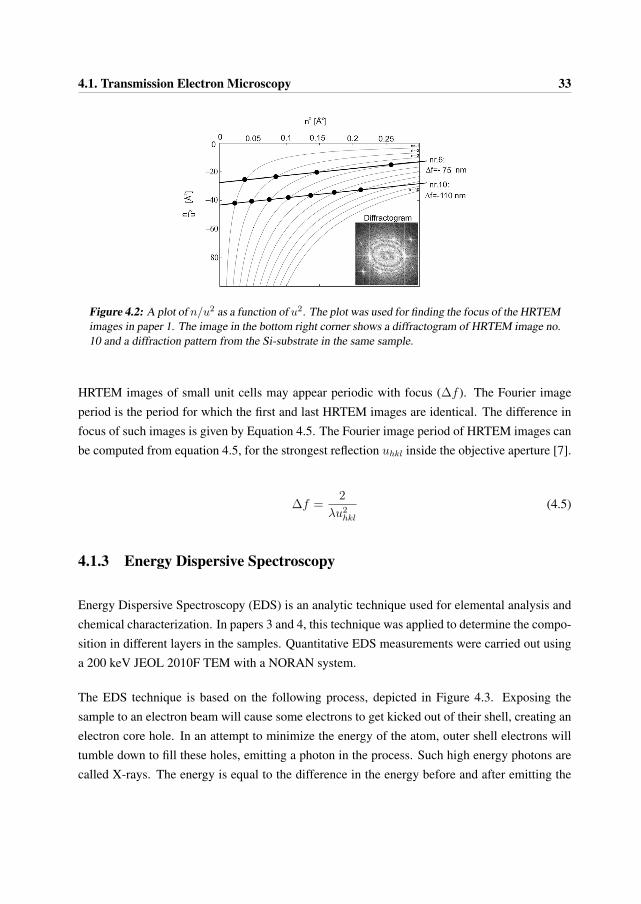
4.3 The EDS process. . . . . . . . . . . . . . . . . . . . . . . . . . . . . . . . . . . 34
4.4 De-excitation mechanism for an atom that has undergone K-shell ionization andsubsequently emission of a characteristic Kβ X-ray. . . . . . . . . . . . . . . . . 36
4.5 An EELS spectrum of Si showing the different peaks present, with an energydispersion of about 0.8 eV. The inserted EELS image has a lower count on they-axis (102). . . . . . . . . . . . . . . . . . . . . . . . . . . . . . . . . . . . . . 37
4.6 The figure exhibits how an EFTEM-SI image is made up of an EELS spectrumin each point in the 2-dimensional image. The image at the top is made by theplasmon peak of Si, which lies at 16.8 eV. (Adapted from Ahn[11].) . . . . . . . 38
xi
xii LIST OF FIGURES
4.7 The figure shows a sketch of Z-contrast/mass-thickness imaging. Thicker regionsor regions with higher atomic number scatter more electrons off axes, causingthem to show up as darker areas in the image. (Adapted from Williams andCarter [4].) . . . . . . . . . . . . . . . . . . . . . . . . . . . . . . . . . . . . . 39
4.8 A survey spectrum of the sample investigated in paper 4, containing Si, SiO2,Ge, and Pd. . . . . . . . . . . . . . . . . . . . . . . . . . . . . . . . . . . . . . 40
4.9 The scattering process of a photon resulting in a photoelectron and an Augerelectron. The figure is adapted from a book by Niemantsverdriet [13]. . . . . . . 41
4.10 The take-off angle φ and angle of emission θ. . . . . . . . . . . . . . . . . . . . 434.11 A Wagner diagram plotted from the work in paper 1, of the samples with crys-
talline and amorphous Si nanoclusters. . . . . . . . . . . . . . . . . . . . . . . . 53
5.1 A cross-sectional sample glued on a Cu slot. . . . . . . . . . . . . . . . . . . . . 585.2 Cu nanoclusters in SiO2, introduced during surface preparation with too small
grazing incidence angle of the sputter beam in the ion etcher. . . . . . . . . . . . 59
Chapter 1
Introduction
Memory storage devices have been around since the 1960s, when Read Only Memories (ROM)were developed [1, 2, 3]. The ROMs could store up to hundreds or a few thousands bits ofinformation, which is very small compared to today’s technologies.
The first memory storage devices developed were Nonerasable Nonvolatile Memory Devices(NNMD). Nonvolatile means that no power is needed to maintain the information stored in thechip. These devices were built using small fuses, each of which represented one storage location,or 1 bit, where a blank ROM would have all fuses intact. Two types of NNMDs were developed,Programmable Read Only Memories (PROM) [4] and Mask Read Only Memories (MROM).PROM used the same concept as ROMs, but offered the convenience of programmable via aprogrammer, which means that the user had the ability to use a PROM programmer from hislocation and not have this task done for him. This device was still popular in the early 1970s.
Unfortunately the production of PROMs in mass quantities was time consuming and cumber-some. In the early 1980s MROMs were developed. The new MROMs used a code correspondingto the 0 or 1 pattern that needed to be programmed into the device. The manufacturer would thenbuild a mask corresponding to this pattern and would use this mask to program a very large num-ber of ROM. They could therefore achieve higher manufacturing efficiency and lower cost perdevice than was possible with pure ROM devices, and the MROMs were growing to quantitiesof millions of pieces per month in some applications. Their use continues in some applicationstoday [2].
1
2 Chapter 1. Introduction
Erasable Nonvolatile Memory Devices as Erasable Programmable Read Only Memories (EPROM),One-Time Programmable Memories (OTP), and Electrically Erasable Programmable Read OnlyMemories (EEPROM) were discovered in the 1970s - 1980s. EPROM were discovered in 1971by Dr Dov Frohman of Intel Corporation [1, 2, 3]. The basic storage element in an EPROMis a Metal-Oxide Semiconductor (MOS) transistor that has an additional floating gate built inbetween the control gate and the channel. The cell has a threshold voltage or a gate voltage atwhich the cell begins to conduct. When programming the device, an elevated voltage is appliedto the gate and the drain of the cell. The electrons will then penetrate the oxide into the floatinggate, thereby altering the threshold voltage of the cell by 5-10 V. The oxide is perfectly isolatedby an insulator (ex. SiO2), so that injected electrons cannot leak out of the floating gate afterpower is removed.
The production costs and time are significantly lower for EEPROMs than for standard PROMs.The EPROMs could erase an EPROM and reprogram it with the modified program, rather thanhaving to incur the cost of a new PROM and wait the needed time for it to be programmedevery time a new version of the software is written. The EPROMs became therefore the favouredmemory device for product development and manufacture of end product with total productionrun of 10 000 units or less.
OTP gained popularity in the early-to-mid 1990s, to the point that they were used in millions ofpieces per month in several applications. The OTP allows user to program them just once, butwould be lower in cost than EPROMs, since they were housed in plastic packages as opposed toceramic packages used for EPROMs. Today there are only a few companies that use the OTPmemory device.
EEPROM devices could be erased and programmed in-circuit, as opposed to EPROMs that onlycould be programmed outside the circuit in which they are used. This could be done by ex-posing the cells to an electric charge. The device can only be erased a finite number of timesbecause of the dielectric breakdown characteristics of the charge transfer oxides and the trappedcharge in the oxides that eventually builds up to a level that causes improper operation. EarlierEEPROMs offered an endurance of only 100 program/erase cycles, while today’s EEPROMshave improved this number to 10 000 program/erase cycles. Although newer technologies havereplaced EEPROMs in many high-volume applications, EEPROMs still find use in some of to-day’s applications.
3
Flash memory devices were developed in the early 1980s, when it became clear that the need forsome upcoming applications surpassed the cumbersome byte-erase capability of the devices justdiscussed. The system performance could be much higher if the entire memory array or a largeportion thereof could be erased quickly, so that new data could be written in its place.
Flash memory was implemented by Masuoka and Hisakazu [5, 6]. They worked at ToshibaCorporation and had already applied for a patent for simultaneously erasable EEPROMs in 1980.Two types of flash memory devices were developed, called NOR and NAND. The NOR andNAND gates are digital logic gates that implement logical NOR or NAND (truth-functionaloperator which produces a result that is the negation of logic) according to given tables. The newmemory cell had only one cell which consisted of only one transistor. This costs far less thanbyte-programmable EEPROM and therefore has become the dominant technology wherever asignificant amount of non-volatile, solid state storage is needed. The single-transistor cell hasa simultaneous multibyte-erase scheme. Flash memory offers fast read access times and betterkinetic shock resistance than hard discs. Also, when packaged in a memory card, it is extremelydurable, being able to withstand intense pressure, extremes of temperature, and even immersionin water. The device has slow erase cycles, which means that the large block sizes used inflash memory erasing gives it speed advantage over the old style EEPROM when writing lotsof data. Masuoka [5, 6] started working on a test chip in 1983, which led in 1985 to Toshiba’spresentation, at the International Solid-State Circuits Conference (ISSCC), of a 256 kbit flashEEPROM device. This flash memory device uses a dual gate structure, in which the gate furtherfrom the silicon substrate is dubbed as the control gate, and the gate closer to the silicon substrateis dubbed the floating gate. Flash memory is mostly used in memory cards and USB (UniversalSerial Bus) flash drives, for storage and transfer of data, and the use of this is discussed in thenext chapter.
Silicon is widely used for electronic devices and is one of our most important semiconduc-tor materials. It is used as floating gate in the memory devices, while SiO2 is often used asthe tunnel oxide, because of its good dielectric properties. One of the most important devel-opments within the microelectronics industry is scaling the Si Complementary-Metal-Oxide-Semiconductor (CMOS) transistors down in size and generally improving the device further.The main challenges at nanoscale level are power and performance optimization, device fabrica-tion, and control of variations at the nanoscale and integration of a diverse set of materials anddevices on the same chip. A key element in one of the proposed schemes to meet future demandsof downscaling is replacing the polycrystalline Si floating gate by nanocrystals. This can also
4 Chapter 1. Introduction
improve writing times, lower the gate voltage and lower the power consumption.
In this thesis, nanoclusters of Si, Ge, Er, and Pd were embedded in an SiO2 film, in order tostudy their composition, nucleation, distribution, and atomic and electronic structure with dif-ferent heat treatments and compositions. This was done using High Resolution TransmissionElectron Microscopy (HRTEM), Energy Filtered TEM (EFTEM), X-ray Photoelectron Spec-troscopy (XPS), Electron Energy Loss Spectroscopy (EELS), Secondary Ion mass Spectroscopy(SIMS), and Energy Dispersive X-ray Spectroscopy (EDS).
References
[1] P. CAPPELLETTI, C. GOLLA, P. OLIVO, and E. ZANONI, Flash Memories, Springer, 1999.
[2] V. G. OKLOBZIJA, Digital Design and Fabrication, CRC Press, 2007.
[3] F. E. VALDES-PEREZ, V.-P. F. E. STAFF, and R. PALLAS-ARENY, Microcontrollers: Fun-
damentals and Applications with PIC, CRC Press, 2009.
[4] US-Switch Matrix- Patent 3028659.
[5] WWW.FORBES.COM, 2009.
[6] F. MASUOKA and I. HISAKAZU, US patent 4531203.
Chapter 2
Nanostructured Memory Devices
Nanostructured memory devices are suggested to be an improvement to the flash memory devicesused today. Nanocrystals have the potential to be used in different applications, such as opticalamplifiers, photon converters, and memory storage devices [1, 2, 3, 4] to mention just a few.Nanocrystal memory cells have potentially better electronic performance than current technologyoffers, and those properties in combination with features inherent in the concept is consideredto yield a possibility for scaling the devices considerable down in size which is desired fromeconomic and technological reasons. An interesting property of semiconductor nanocrystals isits ability to store charge over time at room temperature when embedded in an oxide layer.
This chapter contains a short introduction to quantum dots and flash memory devices. In addition,expected improvements from the usage of nanocrystals instead of the normal bulk floating gateare given.
2.1 Quantum dots
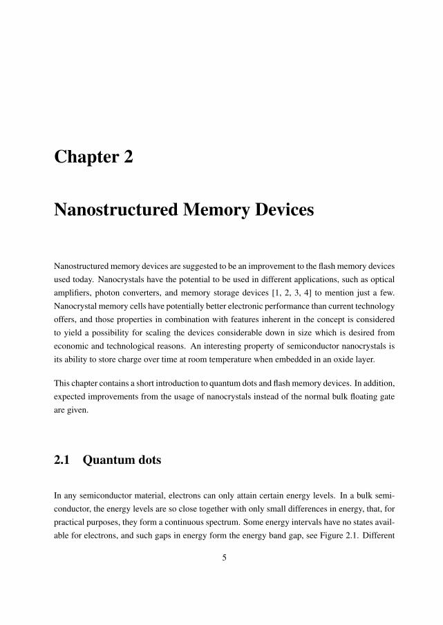
In any semiconductor material, electrons can only attain certain energy levels. In a bulk semi-conductor, the energy levels are so close together with only small differences in energy, that, forpractical purposes, they form a continuous spectrum. Some energy intervals have no states avail-able for electrons, and such gaps in energy form the energy band gap, see Figure 2.1. Different
5
6 Chapter 2. Nanostructured Memory Devices
Figure 2.1: A sketch of the energy bands and dielectric function of an atom, a bulk material and ananocrystal quantum dot, adapted from Bimberg, Grundmann and Ledentsov [5] and Borovitskayaand Shur [6].
semiconductor materials have different band gaps, and quantum dot nanocrystals, being madefrom semiconductor materials, are therefore characterized by their band gaps.
In what follows, the different regimes for the so called confinement will be discussed with regardsto the size of the confinement.
If the size of the nanocrystals is of the same order as the exciton Bohr radius and the de Brogliewave length, the energy levels cannot be described as continuous. Instead, they occupy discreteenergy levels (quantum confinement), and size quantization effects can be observed [7, 5]. Thismeans that quantum dots have large level spacing with a defined boundary between the matrixand the quantum dot. Because of their discrete energy levels, the quantum dots are more relatedto an atom than to a bulk material, see Figure 2.1.
The exciton Bohr radius is the distance between an excited electron and the corresponding hole(electron-hole pair), see Figure 2.1. The exciton Bohr radius and an evaluation of the quantumconfinement with varying quantum dot radius is presented. The radius can be calculated fromthe sub-band energy separation (Esub−band) and the exciton binding energy (Eexciton
B ) [8]. The
2.1. Quantum dots 7
sub-band energy separation (Esub−band) of the electron or the corresponding hole is given by [8]
Esub−band =�
2D
2me(h)R2(2.1)
where R is the quantum dot radius, me(h) is the effective mass of the electron (hole) and D is anumerical factor. This factor depends on the shape of the quantum dot and is typically about 10for a spherical quantum dot. The exciton binding energy (Eexciton
B ) in the bulk is given by [8]
EexcitonB =
�2
2μ(a∗B)2
(2.2)
where μ is the electron-hole reduced mass and a∗B is the exciton Bohr radius. When assuming
me � mh, the criterion for higher hole sub-bands to be included is given by Esub−band ≤ EexcitonB
[8]. That is
D
mhR2≤ 1
me(a∗B)2
(2.3)
which can be rewritten to
(R
a∗B
)2
≥ me
mh
D (2.4)
At strong quantum confinement the quantum dot radius is much smaller than the exciton Bohrradius, i.e. R/a∗
B � 1. At that point the EexcitonB is of the order of Esub−band and much lower
than the electron-hole Coulomb interaction, and the exciton ground state is mainly composed ofthe lowest-energy sub-band states. As the quantum dot radius increases, the energy separation ofthe sub-bands becomes comparable with Eexciton
B , and it can even get smaller. In this region thereis intermediate confinement, and higher sub-band states are even mixed into the exciton groundstate. Increasing the quantum dot radius further results in weak quantum confinement. Herethe quantum dot radius is much larger than Eexciton
B , and the sub-bands are distributed almostcontinuously. The electron-hole binding energy is nearly the same as in the bulk material [8].
8 Chapter 2. Nanostructured Memory Devices
The de Broglie wave length (λ) can be expressed as [6]
λ =h
p=
6.22√meff
m0
T300
(2.5)
where p the particle momentum, h is Planck’s constant, meff is the effective electron mass, m0 isthe electron mass, and T the temperature. The de Broglie wave length varies from a fraction ofone nanometer to 10-20 nm.
Because the energy levels of the quantum dot are discrete rather than continuous, adding orextracting only one electron can change the properties of the quantum dot dramatically, likealtering the boundaries of the band gap. Variations in the geometry of the quantum dot can alsoalter the band gap. Because of the small size of the quantum dot, the band gap will always belarger than for the same semiconductor bulk material.
2.2 Traditional flash memory devices
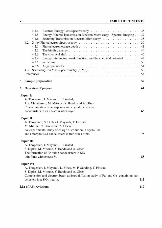
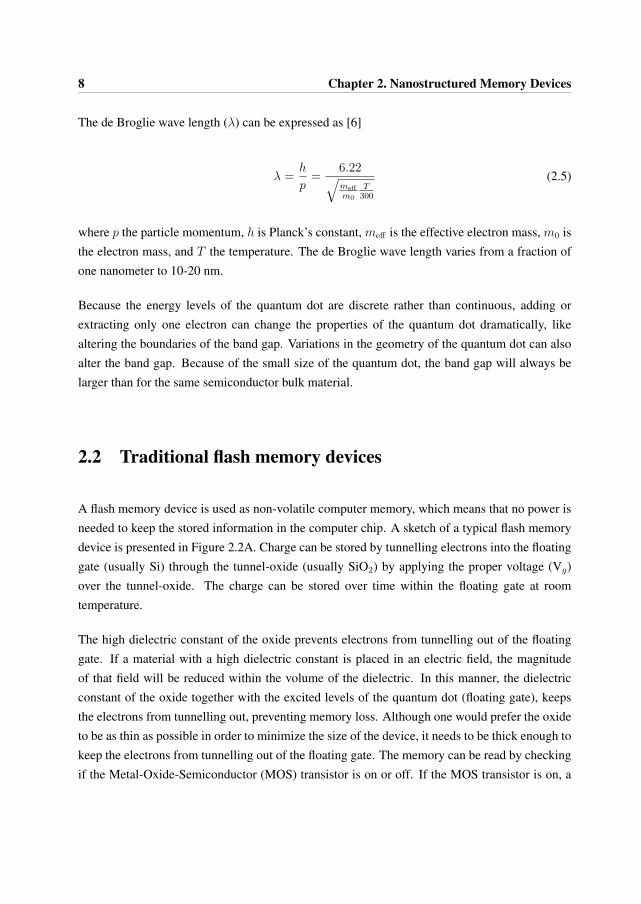
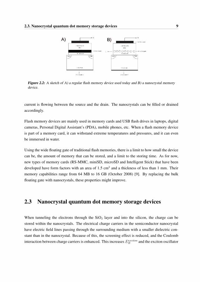
A flash memory device is used as non-volatile computer memory, which means that no power isneeded to keep the stored information in the computer chip. A sketch of a typical flash memorydevice is presented in Figure 2.2A. Charge can be stored by tunnelling electrons into the floatinggate (usually Si) through the tunnel-oxide (usually SiO2) by applying the proper voltage (Vg)over the tunnel-oxide. The charge can be stored over time within the floating gate at roomtemperature.
The high dielectric constant of the oxide prevents electrons from tunnelling out of the floatinggate. If a material with a high dielectric constant is placed in an electric field, the magnitudeof that field will be reduced within the volume of the dielectric. In this manner, the dielectricconstant of the oxide together with the excited levels of the quantum dot (floating gate), keepsthe electrons from tunnelling out, preventing memory loss. Although one would prefer the oxideto be as thin as possible in order to minimize the size of the device, it needs to be thick enough tokeep the electrons from tunnelling out of the floating gate. The memory can be read by checkingif the Metal-Oxide-Semiconductor (MOS) transistor is on or off. If the MOS transistor is on, a
2.3. Nanocrystal quantum dot memory storage devices 9
Figure 2.2: A sketch of A) a regular flash memory device used today and B) a nanocrystal memorydevice.
current is flowing between the source and the drain. The nanocrystals can be filled or drainedaccordingly.
Flash memory devices are mainly used in memory cards and USB flash drives in laptops, digitalcameras, Personal Digital Assistant’s (PDA), mobile phones, etc. When a flash memory deviceis part of a memory card, it can withstand extreme temperatures and pressures, and it can evenbe immersed in water.
Using the wide floating gate of traditional flash memories, there is a limit to how small the devicecan be, the amount of memory that can be stored, and a limit to the storing time. As for now,new types of memory cards (RS-MMC, miniSD, microSD and Intelligent Stick) that have beendeveloped have form factors with an area of 1.5 cm2 and a thickness of less than 1 mm. Theirmemory capabilities range from 64 MB to 16 GB (October 2008) [9]. By replacing the bulkfloating gate with nanocrystals, these properties might improve.
2.3 Nanocrystal quantum dot memory storage devices
When tunneling the electrons through the SiO2 layer and into the silicon, the charge can bestored within the nanocrystals. The electrical charge carriers in the semiconductor nanocrystalhave electric field lines passing through the surrounding medium with a smaller dielectric con-stant than in the nanocrystal. Because of this, the screening effect is reduced, and the Coulombinteraction between charge carriers is enhanced. This increases Eexciton
B and the exciton oscillator
10 Chapter 2. Nanostructured Memory Devices
strength compared to the situation with a surrounding matrix with the same dielectric constant asSi or by pure Si [8]. Between the nanocrystal and the matrix, there is a potential barrier actingsuch that the electrons are trapped within the nanocrystal. As the quantum dots are small, addingor removing only one electron will alter the material properties on a large scale. Because ofthis, the properties of the nanocrystals are somewhere between those of bulk semiconductors andthose of discrete molecules.
By replacing the bulk floating gate with nanocrystals, longer retention may result in lower gatevoltage and lower power consumption [10]. The non-continuity between the nanocrystals canalso prevent charge loss laterally and result in short writing times at lower voltages and improvedreliability [11]. Nanocrystals with a diameter of less than 10 nm are desirable, since the Coulombblockade effect becomes prominent at room temperature [12]. When the dimensions approachthe atomic scale, nanocrystals start to differ significantly from bulk materials in their electronic,optical and thermodynamic properties [13]. In these nanocrystal memory devices, the processesof injection and retention of electrons are very sensitive to the size, distribution, interfaces andelectronic structure of the nanocrystals. It is therefore important to study the nucleation mech-anisms of the nanocrystals, their crystal structure, defects, and distribution, in order to makedevices in a controlled manner. The devices need an accurate control of the array of nanocrys-tals, since changing the tunnel distance by only one nanometer can affect the write and erasetime [14].
2.4 Basic requirements for quantum dots in room tempera-ture devices
Some of the basic requirements for quantum dots operating at room temperature are discussedbelow. As discussed above, the quantum dots should be small. There is, however, a lower sizelimit. This critical diameter size Dmin occurs where at least one energy level of an electron orhole is present [5]. This lower size limit depends strongly on the band offset of the correspondingbands in the material system. One electron level exists only if the confinement potential exceedsthe value Dmin, which is defined by [5]
2.4. References 11
Dmin =π�√
2m∗eΔEc
(2.6)
where m∗e is the effective electron mass and ΔEc is the conduction band offset.
A certain level of uniformity in size, shape, and chemical composition are needed to get a sta-ble device. In addition, the nanocrystal quantum dots should be free of defects like dislocationsand twins. The size fluctuations cause a variation in the energy position of the electronic lev-els. Quantum dots rely on the integrated gain in narrow energy range, which means that theinhomogeneous energetic broadening should be as small as possible [5].
References
[1] S. TIWARI, F. RANA, H. HANAFI, A. HARTSTEIN, E. F. CRABBE, and K. CHAN, Appl.
Phys. Lett. 68, 1377 (1996).
[2] H. S. HAN, S. Y. SEO, and J. H. SHIN, Appl. Phys. Lett. 79, 4568 (2002).
[3] P. KIK and A. POLMAN, J. Appl. Phys. 91, 534 (2002).
[4] L. PAVESI and D. J. LOCKWOOD, Silicon Photonics, Springer-Verlag, 2004.
[5] D. BIMBERG, M. GRUNDMANN, and N. LEDENTSOV, Quantum Dot heterostructures,Wiley, 1999.
[6] E. BOROVITISKAYA and M.S.SHUR, Quantum dots, Low dimensional systems, chapter 1,p. 1, World Scientific, 2002.
[7] WWW.EVIDENTTECH.COM, 2008.
[8] Y. MASUMOTO and T. TAKAGAHARA, Semiconductor Quantum Dots: Physics, Spec-
troscopy, and Applications, Springer, 2002.
[9] http://www.sandisk.com/Corporate/PressRoom/PressReleases/PressRelease.aspx?ID=4398,2008.
12 Chapter 2. Nanostructured Memory Devices
[10] T. P. CHEN, Y. LIU, C. Q. SUN, M. S. TSE, J. H. HSIEH, Q. Y. FU, Y. C. LIU, , andS. FUNG, J. Phys. Chem. B 108, 16609 (2004).
[11] F. KARADAS, G. ERTAS, and S. SUZER, J. Phys. Chem. B 108, 1515 (2004).
[12] S. NAITO, M. SATAKE, H. KONDO, M. SAKASHITA, A. SAKAI, S. ZAIMA, and Y. YA-SUDA, Jpn. J. Appl. Phys. 43, 3779 (2004).
[13] T. MOHANTY, N. C. MISHRA, A. PRADHAN, and D. KANJILAL, Surf. Coat. Technol.
197, 34 (2005).
[14] M. PEREGO, S. FERRARI, M. FANCIULLI, G. B. ASSAYAG, C. BONAFOS, and A. C.M. CARRADA, Appl. Surf. Sci. 231-232, 813 (2004).
Chapter 3
Materials
In this chapter, a brief introduction to the different material systems studied in this work is pre-sented. In the papers presented in this work, samples containing Si, Ge, Er, and Pd nanoclusterswere studied in detail. In the following sections the samples and their sample processing condi-tions are discussed in detail.
3.1 Si nanocluster samples
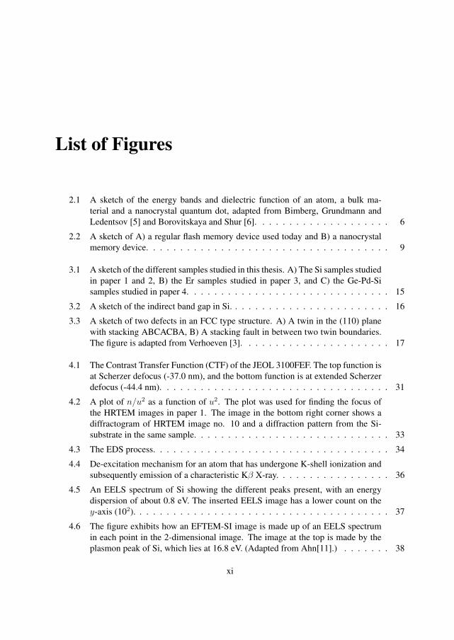
In papers 1 and 2, amorphous and crystalline nanoclusters of Si were studied. These sampleswere made by growing a ∼3 nm thin layer of SiO2 on a p-type silicon substrate by Rapid ThermalOxidation (RTO) at 1000◦C for 6 seconds. By precise control of the oxidation temperature andreducing the thermal budget of the heat cycle required for an oxide film growth, the effects ofoxidation on the impurity profile can be controlled and minimized.
Prior to growing the RTO layer, the wafers were cleaned using a standard RCA procedure (RadioCorporation of America, industry standard for removing contaminants from wafers [1]) followedby immersion in a 10 % HF solution to remove the native oxide. Then a ∼10 nm layer of siliconrich oxide was sputtered from a SiO2:Si composite target onto the RTO and heat-treated in a N2
atmosphere at 1000 − 1100◦C for 30-60 minutes. Different area percentages (defined below) ofSi:SiO2 (6, 8, 17, 28, 42, 50, 60, 70 area % or about 4, 5, 11, 18, 33, 40, 46 atomic %) were
13
14 Chapter 3. Materials
used to produce different silicon super saturation in the oxide. A sketch of this type of samplesis presented in Figure 3.1A for the cases where Si nanoclusters have formed in the oxide.
The atomic percentage of the different elements in the sample can be calculated from the areapercentages. The equation for the atomic percentage of excess Si in SiO2 is
atomic% =area%(SiSi) · spc(SiSi)
area%(SiSi) · spc(SiSi) + area%(SiO2) · (spc(SiSiO2) + spc(OSiO2))(3.1)
where the sputtering coefficients (spc) are 0.7622 for Si in pure Si, 1.88 for Ge in pure Ge, 2.42for Er in pure Er, 0.295 for Si and 0.622 for O in SiO2.
3.1.1 Silicon properties
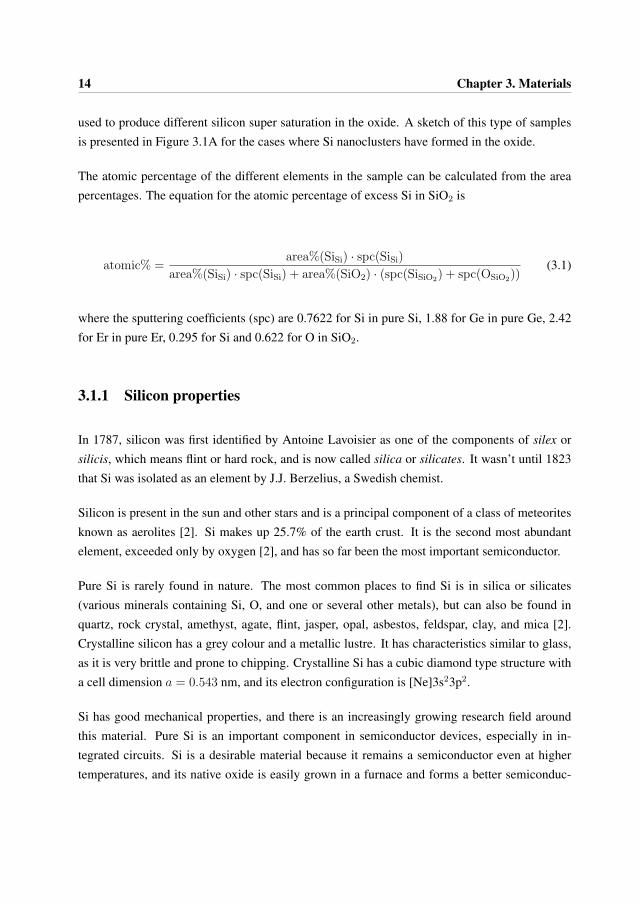
In 1787, silicon was first identified by Antoine Lavoisier as one of the components of silex orsilicis, which means flint or hard rock, and is now called silica or silicates. It wasn’t until 1823that Si was isolated as an element by J.J. Berzelius, a Swedish chemist.
Silicon is present in the sun and other stars and is a principal component of a class of meteoritesknown as aerolites [2]. Si makes up 25.7% of the earth crust. It is the second most abundantelement, exceeded only by oxygen [2], and has so far been the most important semiconductor.
Pure Si is rarely found in nature. The most common places to find Si is in silica or silicates(various minerals containing Si, O, and one or several other metals), but can also be found inquartz, rock crystal, amethyst, agate, flint, jasper, opal, asbestos, feldspar, clay, and mica [2].Crystalline silicon has a grey colour and a metallic lustre. It has characteristics similar to glass,as it is very brittle and prone to chipping. Crystalline Si has a cubic diamond type structure witha cell dimension a = 0.543 nm, and its electron configuration is [Ne]3s23p2.
Si has good mechanical properties, and there is an increasingly growing research field aroundthis material. Pure Si is an important component in semiconductor devices, especially in in-tegrated circuits. Si is a desirable material because it remains a semiconductor even at highertemperatures, and its native oxide is easily grown in a furnace and forms a better semiconduc-
3.1. Si nanocluster samples 15
Figure 3.1: A sketch of the different samples studied in this thesis. A) The Si samples studied inpaper 1 and 2, B) the Er samples studied in paper 3, and C) the Ge-Pd-Si samples studied in paper 4.
16 Chapter 3. Materials
Figure 3.2: A sketch of the indirect band gap in Si.
tor/dielectric interface than any other material. The raw materials are relatively cheap, and theintegrated opto-electronic silicon can be used in telecommunication, information technology, andmicrotechnology.
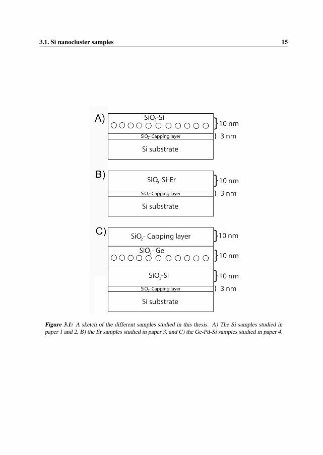
As depicted in Figure 3.2, Si has an indirect band gap, which is the energy gap in which the min-imum energy in the conduction band is shifted by a k-vector (difference in momentum) relativeto the valence band.
When electrons are excited to the conduction band, the electrons quickly settle into the energyminimum. For the electrons to fall back into the valence band, the electrons require extra mo-mentum allowing them to overcome the offset. Emitted and absorbed photons have high energy,but negligible momentum compared to this energy offset. Because of this, indirect semicon-ductor materials are inefficient for emitting light, which involves electron-hole recombination.Electron-hole recombination can therefore take some time and take place preferentially at pointdefects, dislocations or at grain boundaries.
The absorption of light at an indirect band gap is weaker than at a direct band gap. The onlyway for an electron to jump from the valence band maximum to the conduction band minimumis to simultaneously emit or absorb a phonon. This would then compensate for the missingmomentum (k-vector), but this transition has a very low probability.
3.1. Si nanocluster samples 17
Figure 3.3: A sketch of two defects in an FCC type structure. A) A twin in the (110) plane withstacking ABCACBA, B) A stacking fault in between two twin boundaries. The figure is adaptedfrom Verhoeven [3].
3.1.2 Defects
Silicon has a diamond type FCC crystal structure, where some of the most common defects arepoint defects, dislocations, twinning, and stacking faults. In paper 1, nanocrystals containingtwins and stacking faults were found. These defects and their effects upon the memory deviceare discussed below.
Twinning is a change in stacking sequence over many atomic layers that results in two crystallinegrains sharing some of the same crystalline positions at the interface [3]. This interface withshared atomic sites separating the two crystals is called the twin boundary. A sketch of a twin inan FCC crystal structure is shown in Figure 3.3A. The twinned stacking sequence shown in theFigure is ABC A CBA, where the twin boundary is at the A position in the middle. The twinningresults in a mirror image of the other crystal grain.
Twinning can be formed in a crystal in different manners, like during deformation or crystal
18 Chapter 3. Materials
growth [3]. A Growth twin can be formed as a result of changes in the stacking during growth.They can be formed in a crystal whether it is growing from vapor, liquid, or solid state. Anothertwin formation is called Annealing or Transformation twin. This can occur as a result of changesin the crystal systems during cooling. One form becomes unstable and the crystal structure mustre-organize or transform into another more stable form. It is common for FCC type metals toform growth twins during relaxation. A third twin formation is called Deformation or Glidetwin. This twin formation is a result of stress on the crystal after the crystal has formed. Duringdeformation of metals, slip is generally more easily generated than twinning. Twinning will onlybe a significant mechanism for plastic deformation in non-cubic metals (ex. Hexagonal ClosedPacked (HCP) metals). This type of metals has only a few slip systems available. Deformationtwinning in FCC type metals are rare and may only occur at very low temperatures [3].
Stacking faults are two dimensional defects that can be seen as a change in stacking sequenceover a few atom spacings, see Figure 3.3B. In the figure, twin orientation I and III have identicalcrystallographic orientations. Region II is separated from region I and III by two twin boundaries.If this region is separated by a few nanometers, it will be called a twin. If it is separated by onlya few atomic spacings, it will be called a stacking fault [3]. The stacking fault is in a sense twotwin boundaries and can be made up by only one atomic plane, as in ABCAB A BCABC.
Twinning depends on the stacking fault energy of the material, the crystallographic orientation,surface stresses, and surface orientations [4, 5]. Defects and imperfections either inside thenanocrystal or at the nanocrystal/oxide interface can have large effects upon the operationalcharacteristics of the device [5, 6, 7, 8]. Nanocrystal twinning can be due to stress inside thenanocrystal and on the surface, coalescence of smaller nanocrystals, or it can occur duringgrowth/heat-treatment.
3.2 Er-Si nanocluster samples
In paper 3, SiO2 with both Er and Si were made by growing a ∼3 nm layer of SiO2 on a p-typeSi substrate by Rapid Thermal Oxidation (RTO) at 1000oC for 6 sec. Then a layer of Er-dopedSi rich oxide was sputtered from a SiO2:Si:Er composite target onto the RTO with a 30 nm oxidethickness. The percentages of Si and Er are 17 area % (11 at. %) and 1.1 area % (1 at. %)respectively. The samples were then heat treated in a N2 atmosphere at 1000− 1100oC for 30-60
3.3. Ge-Si-Pd nanocluster samples 19
min. A sketch of the samples discussed in this paper is presented in Figure 3.1B.
3.2.1 Erbium properties
The name Erbium (Er) originates from a town in Sweden called Ytterby where large concen-trations of Yttria and Erbium were found. The material was discovered in 1843 by Carl GustafMosander. In 1905 Georges Urbain and Charles James isolated ErO2, but pure Er wasn’t pro-duced until 1934, when workers reduced the anhydrous chloride with potassium vapour.
Er is a silvery, white, metallic, rare earth element. Pure Er is easily shaped, does not oxidize aseasily as other rear earth elements, and is stable in air. Erbium’s properties partly depend on theamount and type of impurities present in the material. This element cannot be found as a pureelement in nature, but is found bound in monazite and sand ores.
The (indirect) excitations of Er atoms from Si nanocrystals are useful for optical applications,like light-emitting diodes and lasers [9, 10]. Si was for a long time considered unsuitable foroptoelectronic applications due to silicon’s indirect band gap and the absence of linear electro-optic effect. However, doping of Er into the Si structure has avoided this problem [11]. The Erelectronic configuration of Er is [Xe]=4f126s2, with an electron shell structure of: 2,8,18,30,8,2[2]. This shows that Er has an unfilled 4f shell surrounded by an external closed shell [11]. Intra4f-transitions (4l13/2 to 4l15/2) will therefore show luminescence at 1.54 μm, which is concordantwith the absorption minimum in silicon-based glass fibers [10, 12]. This transition can be excitedboth optically [13] and electrically [14]. The sensitizing of Er by Si nanocrystals have beenstudied by many authors and is currently an active field of research [15, 16, 17, 18, 19, 20].
3.3 Ge-Si-Pd nanocluster samples
In paper 4, Ge and Pd nanoclusters in the presence of pure Si were studied. The samples wereproduced by growing a ∼3 nm layer of SiO2 on a p-type silicon substrate by Rapid ThermalOxidation (RTO) at 1000oC for 6 sec. Prior to growing the RTO layer the wafers were cleanedusing a standard RCA procedure (Radio Corporation of America, industry standard for removingcontaminants from wafers) followed by immersion in a 10 % HF solution to remove the native
20 Chapter 3. Materials
oxide. After the RTO growth a ∼10 nm layer of silicon rich oxide was sputtered from a SiO2:Sicomposite target onto the RTO-SiO2 and heat treated in N2 atmosphere at 1000oC for 30 min.Different area percentages (area coverage by the sputtered material) of Si:SiO2 ( 28, 42, 50, 60,70% or 4, 5, 11, 33, 40, 46 at. %) were achieved. A ∼10-13 nm Ge rich (3.3 area %) SiO2
with a 10 nm SiO2 capping layer was then sputtered onto the Si rich oxide, with a subsequentheat-treatment at 900oC for 30 min to nucleate Ge nanocrystals. A sketch of the material systemsdiscussed in this paper is presented in Figure 3.1C. During this last procedure, contamination ofPd occurred. This contamination resulted in a creation of Pd nanocrystals in the sample. Thesenanoclusters were studied in detail.
3.3.1 Germanium properties
Ge was predicted by Dmitri Mendeleev in 1871 to exist as a missing analogue of the silicongroup [21]. Ge was first proven to exist in 1886, by Clemens Winkler, a German chemist [22].The Ge transistor was developed in 1948 [23]. This discovery resulted in a demand for usingGe in solid state electronics devices [24]. Ge has favourable properties utilized in several opticand electronic devices, such as photo detectors and single transistors [25, 26]. Potential futureapplications may also exploit these for example in photo detectors [27], light emitters [28], singleelectron transistors [29], and non-volatile memories [30].
Ge is a hard, lustrous, greyish-white metalloid. In its pure state it is crystalline, brittle and retainsits lustre in air at room temperature. Ge has an indirect band gap and has an FCC crystal structure(Fm-3m) with a cell dimension a = 0.566 nm, and the electronic configuration is [Ar]3d104s24p2
[2].
Substantial research has previously been devoted to characterizing Ge nanocrystal nucleation,diffusion, and growth [31, 32, 33, 34, 35, 36, 37, 38, 39]. Ge implantation in SiO2 layers hasso far been extensively studied for their photoluminescence and structural properties. Ge is alsoof interest because of its smaller bandgap, inducing a theoretically better retention and fasterwriting/erasing times [40, 41].
3.3. Ge-Si-Pd nanocluster samples 21
3.3.2 Palladium properties
Pd is a silvery white metal that was discovered in 1803 by William Hyde Wollaston [42, 43]. Henamed the metal Pallas after the asteroid which was discovered two years earlier.
Palladium, platinum, rhodium, ruthenium, iridium, and osmium form a group of elements called“platinum group metals” (PGMs). These metals share similar chemical properties. Pd has thelowest melting point and is the densest of these metals. During annealing Pd gets soft and ductile.At room temperature Pd can absorb 900 times its own volume of hydrogen, which makes Pd anefficient and safe storage medium for hydrogen isotopes.
Pd is mostly used for catalytic converters in auto mobiles [44], but can also be found in electronicdevices such as computers, mobile phones, multi-layer ceramic capacitors, component plating,low voltage electrical contacts, and televisions [45]. The metal can also be used in dentistry [46],hydrogen purification, chemical applications, medicine, groundwater treatment, and fuel cells.Considerable research has also been conducted in the use of Pd catalysts for the combustionof methane. Particle morphology and oxidation state can play an important role in definingthe active sites in the Pd catalysts [47]. Pd is also an interesting material used in GranularMetal (GM) films, cermets, or nano-cermets, where metal particles are dispersed in an insulator[48, 49]. The lower dimensional mesoscopic materials with tunnelling junctions have a negativecoefficient of resistance, where the resistance increases with decreasing temperature.
Pure Pd has a Fm-3m space group, with a lattice parameter of 0.389 nm [50]. The electron pershell configuration for Pd is [2]: 2,8,18,18,0. This shows that Pd has an outer closed shell. Pdis a fast interstitial diffuser and almost insoluble in crystalline Si. The solubility of fast diffusingspecies in amorphous Si is known to be higher than that in crystalline Si and very sensitive to thedefect concentration [51]. Pd does not dissolve Ge, and the solubility of Pd in Ge has not beenstudied [52]. Pd in SiO2 has been studied by Ichinohe et al. [48, 49], who studied Pd doped SiO2
films and found at small doses of Pd ultra fine particles of Pd2Si. Voogt et al. [53] studied PdOparticles with a metallic Pd core.
22 Chapter 3. Materials
References
[1] http://fabweb.ece.uiuc.edu/recipe/rca.aspx, 2009.
[2] WEBELEMENTS.COM, The periodic table, 2008.
[3] J. D. VERHOEVEN, Fundamentals of Physical Metallurgy, Wiley, 1975.
[4] H. S. PARK, K. GALL, and J. A. ZIMMERMAN, J. Mech. Phys. Solids 54, 1862 (2006).
[5] Y. Q. WANG, R. SMIRANI, and G. G. ROSS, Nano Lett. 4, 2041 (2004).
[6] C. Q. SUN, L. K. PAN, Y. Q. FU, B. K. TAY, and S. LI, J. Phys. Chem. B Lett. 107, 5113(2003).
[7] Y. Q. WANG and R. S. NAD G. G. ROSS, Appl. Phys. Lett. 86, 221920 (2005).
[8] C. R. PERRY, S. THOMPSON, M. LENTZEN, U. KORTSHAGEN, and C. B. CARTER, J.
Non-Cryst. Solids 343, 78 (2004).
[9] MELDRUM, A. HRYCIW, A. MACDONALD, C. BLOIS, T. CLEMENT, R. DECORBY,J. WANG, and Q. LI, J. Lumin. 121, 199 (2006).
[10] H. ENNEN, J. SCHNEIDER, G. POMRENKE, and A. AXMANN, Appl. Phys. Lett. 43, 943(1983).
[11] C. ZHANG, H. XIAO, Y. WANG, Z. CHENG, X. CHENG, and F. ZHANG, Physica B 362,208 (2005).
[12] M. FUJII, M. YOSHIDA, Y. KANZAWA, S. HAYASHI, and K. YAMAMOTO, Appl.Phys.
Lett. 71, 1198 (1997).
[13] G. FRANZO, F. PRIOLO, S. COFFA, A. POLMAN, and A. CARNERA, Appl. Phys. Lett. 64,2235 (1991).
[14] J. MICHEL, J. BENTON, R. FERRANTE, D. JACOBSON, D. EAGLESHAM, E. FITZGER-ALD, Y.H.XIE, J. POATE, and L. KIMERLING, J. of Appl. Phys. 70, 2672 (1991).
[15] C. CHRYSSOU, D. PACIFICI, V. VINCIGUERRA, F. PRIOLO, and F. IACONA, Appl. Phys.
Lett. 75, 2011 (1975).
3.3. References 23
[16] J. H. SHIN, M. KIM, S. SEE, and C. LEE, Appl. Phys. Lett. 72, 1092 (1998).
[17] P. KIK and A. POLMAN, J. Appl. Phys. 91, 534 (2002).
[18] A. KENYON, C. CHRYSSOU, C. PITT, T. SHIMIZU-IWAYAMA, D. HOLE, N. SHARMA,and C. HUMPHREYS, J. of Appl. Phys. 91, 367 (2002).
[19] F. XU, Z. XIAO, G. CHENG, Z. YI, T. ZHANG, L. GU, and X. WANG, Thin Solid Films
410, 94 (2002).
[20] D. M. ZHIGUNOV, O. SHALYGINA, S. TETERUNKOV, V. Y. TIMOSHENKO,P. KASHKAROV, and M. ZACHARIAS, Semicond. Sci. Technol. 40, 1193 (2006).
[21] M. KAJI, Bull. Hist. Chem. 27, 4 (2002).
[22] C. WINKLER, Ber. Dtsch. Chem. Ges. 19, 210 (1887).
[23] J. BARDEEN, Phys. Rev. B 74, 230 (1948).
[24] National Academy of Engineering (http://www.greatachievements.org/?id=3967), 2008.
[25] S. AGAN, A. DANA, and A. AYDINLI, J. Phys.: Condens. Matter 18, 5037 (2006).
[26] R. SALH, L. FITTING, E. V. KOLESNIKOVA, A. A. SITNIKOVA, M. V. ZAMORYAN-SKAYA, B. SCHMIDT, and H.-J. FITTING, Semiconductors 41, 387 (2007).
[27] K. L. WANG, J. L. LIU, and G. JIN, J. Cryst. Growth 237-239, 1892 (2002).
[28] Y. Q. WANG, G. L. KONG, W. D. CHEN, H. W. DIAO, C. Y. CHEN, S. B. ZHANG, andX. B. LIAO, Appl. Phys. Lett. 81, 4174 (2002).
[29] D. V. AVERIN and K. K. LIKHAREV, J. Low-Temp. Phys. 77, 2394 (1986).
[30] M. KANOUN, , A. S. A. BARON, and F. MAZEN, Appl Phys. Lett. 84, 5079 (2004).
[31] Y. MAEDA, Phys. Rev. B 51, 1658 (1995).
[32] J. VON BORANY, R. GROTZSCHEL, K. H. HEINIG, A. MARKWITZ, B. SCHMIDT,W. SKORUPA, and H. J. THEES, Solid State Electronics 43, 1159 (1999).
[33] W. K. CHOI, Y. W. HO, S. P. NG, and V. NG, J. Appl. Phys. 89, 2168 (2001).
24 Chapter 3. Materials
[34] W. K. CHOI, W. K. CHIM, C. L. HENG, L. W. TEO, V. HO, V. NG, D. A. ANTONIADIS,and E. A. FITZGERALD, Appl. Phys. Lett. 80, 2014 (2002).
[35] M. KLIMENKOV, J. VON BORANY, W. MATZ, R. GROTZSCHEL, and F. HERMANN, J.
Appl. Phys. 91, 10062 (2002).
[36] G. TARASCHI, S. SAINI, W. W. FAN, and L. KIMERLING, J. of Appl. Phys. 93, 9988(2003).
[37] E. S. MARSTEIN, A. E. GUNNÆS, A. OLSEN, T. G. FINSTAD, R. TURAN, and U. SER-INCAN, J. Appl. Phys. 96, 4308 (2004).
[38] W. K. CHOI, V. HO, V. NG, Y. W. HO, S. P. NG, and W. K. CHIM, Appl. Phys. Lett. 86,143114 (2005).
[39] V. BEYER and J. VON BORANY, Phys. Rev. B 77, 014107 (2008).
[40] S. DUGUAYA, A. SLAOUI, J. GROB, M. KANOUN, S. BURIGNAT, and A. SOUIFI, Mater.
Sci. and Engeneer. B 124-125, 488 (2005).
[41] M. KANOUN, A. SOUIFI, T. BARON, and F. MAZEN, Appl. Phys. Lett. 84, 5079 (2004).
[42] W. P. GRIFFITH, Platinum Met. Rev. 47, 175 (2003).
[43] W. H. WOLLASTON, Philos. Trans. R. Soc. London 94, 419 (1804).
[44] J. KIELHORN, C. MELBER, D. KELLER, and I. MANGELSDORF, Int. J. Hyg. Environ.
Health 205, 417 (2002).
[45] S. WANG, J. DOUGHERTY, W. HUEBNER, and J. PEPIN, J. Am. Ceram. Soc. 77, 3051(1994).
[46] R. RUSHFORTH, Platinum Met. Rev. 48 (2004).
[47] P. A. CROZIER, R. SHARMA, and A. K. DATYE, Microsc. Microanal. 4, 278 (1998).
[48] T. ICHINOHE, S. MASAKI, K. UCHIDA, S. NOZAKI, and H. MORISAKI, Thin solid films
466, 27 (2004).
[49] T. ICHINOHE, S. MASAKI, K. KAWASAKI, and H. MORISAKI, Thin solid films 343-344,119 (1999).

3.3. References 25
[50] E. OWEN and E. YATES, Phil. Mag. 15, 472 (1933).
[51] S.-W. LEE, Y.-C. JEON, and S.-K. JOO, Appl. Phys. Lett. 66, 1671 (1995).
[52] Y. D. SEROPEGINA, A. V. GRIBANOVA, and O. I. BODAKB, J. Alloys and Comp. 269,157 (1998).
[53] E. VOOGT, A. MENS, O. GIJZEMAN, and J. GEUS, Surf. Sci. 350, 21 (1996).

Chapter 4
Methodology
4.1 Transmission Electron Microscopy
Transmission Electron Microscopy (TEM) is a set of microscopy based techniques that arewidely used to investigate the structure and properties of different types of materials. The mainingredient of these methods is an electron beam produced by high acceleration voltage that is fo-cused onto a thin sample by means of electromagnetic lenses. The electrons interact strongly withthe sample, creating diffracted beams of electrons, energy loss electrons, X-rays, back-scatteredelectrons, and secondary electrons. The transmitted electrons are then focused by electromag-netic lenses and imaged onto a fluorescent screen.
Scanning Transmission Electron Microscopy (STEM), Electron Energy Loss Spectroscopy (EELS),Energy Filtered Transmission Electron Microscopy - Spectral Imaging (EFTEM-SI), and EnergyDispersive Spectroscopy (EDS) were used to study the composition of the material systems in-vestigated in this work, High Resolution Transmission Electron Microscopy(HRTEM) was usedto study the atomic structure, and EELS was used to study the electronic structure. In the follow-ing sections, these techniques will be discussed in relation to the work presented in four papers.
27
28 Chapter 4. Methodology
4.1.1 Transmission Electron Microscopes
Two microscopes were used to study the nanoclusters in detail. The first microscope was a 200keV JEOL 2010F microscope equipped with a Gatan imaging filter and detector. The spherical(Cs) and chromatic aberration (Cc) coefficients of the objective lens were 0.5 mm and 1.1 mm,respectively. The point to point resolution was 0.194 nm at Scherzer focus (-42 nm). A probecurrent of about 0.5 nA at a probe diameter of 1.0 nm can be obtained. The energy resolution at200 keV can be about 0.8 eV.
The other microscope was a 300 keV JEOL 3100FEF microscope with an Omega energy filter.The spherical and chromatic aberration coefficients of the objective lens were 0.6 mm and 1.1mm, respectively. The point to point resolution was 0.174 nm at Scherzer focus (-37 nm), andthe minimum probe diameter was 0.2 nm. The energy resolution at 300 keV was 0.78 eV andwas previously determined experimentally [1]. The energy dispersion of the Omega-filter was0.85 μm/eV at 300 keV.
4.1.2 High Resolution Transmission Electron Microscopy
As silicon nanocrystals have low contrast when embedded in an SiO2 matrix, it is difficult toobserve them directly in bright field and dark field TEM images. It is, however, possible to dis-tinguish the Si nanocrystals from the amorphous SiO2 matrix by High Resolution TransmissionElectron Microscopy (HRTEM) images showing Si lattice fringes. In papers 1, 3, and 4, thistechnique was applied to study the atomic structure of the nanocrystals and their environment indetail. HRTEM was performed using both the 300 keV JEOL 3100FEF TEM and the 200 keVJEOL 2010F TEM.
The main difference between conventional TEM and HRTEM is that HRTEM creates an imagebased on several beams, while conventional TEM produces an image from only one electronbeam. The images in HRTEM are based upon the interference between the direct beam andthe diffracted electron waves. Different materials give rise to slight phase differences in thewave function of the transmitted electron beams, creating contrast between different areas of theimage. It should be remarked that in many cases this can be described by the weak phase objectapproximation. That is, it is considered that the sample is so thin that the amplitude variations
4.1. Transmission Electron Microscopy 29
have only small effects upon the image [2, 3].
The Contrast Transfer Function (CTF) modulates the amplitudes and phases of the electronbeams as they pass through the objective lens [2, 3]. It defines the point to point resolutionand the information limit of the microscope. The CTF can be represented by
T (u) = − sin(π
2Csλ
3u4 + πΔfλu2)
(4.1)
where λ is the electron wavelength, u is the spatial frequency, Δf is the defocus of the objectivelens, and Cs is the spherical aberration coefficient.
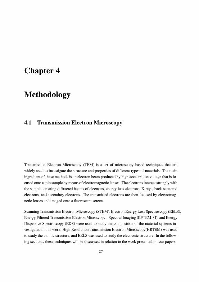
The CTF of the JEOL 3100FEF microscope at Scherzer defocus (-37 nm) and at extendedScherzer defoucs (-44.4 nm) conditions are presented in Figure 4.1. Some important pointsto notice about this function are given below [2, 4]:
• CTF is oscillatory: there are “passbands” where it is not equal to zero (good “transmit-tance”) and there are “gaps” where it is equal (or at least very close to) zero (no “transmit-tance”).
• When it is negative, positive phase contrast occurs, meaning that atoms will appear darkon a bright background for thin samples (near the edge).
• When it is positive, negative phase contrast occurs, meaning that atoms will appear brighton a dark background for thin samples (near the edge).
• When it is equal to zero, there is no contrast (information transfer) for this spatial fre-quency.
• First crossing of the u-axis at Scherzer defocus corresponds to point-to-point resolution ofthe microscope.
• The point where the envelope functions (see below) damp the CTF to 1/e corresponds tothe information limit of the microscope.
Other important features:
30 Chapter 4. Methodology
• CTF starts at 0 and decreases, then
• CTF stays almost constant and close to -1 (providing a broad band of good transmittance),then
• CTF starts to increase, and
• CTF crosses the u-axis, and then
• CTF repeatedly crosses the spatial frequency u-axis as u increases.
• CTF can continue forever, but, in reality, it is modified by envelope functions and eventu-ally dies off. The effect of the envelope functions can be represented as
T (u)eff = T (u)EcEa (4.2)
where Ec is the temporal coherency envelope caused by chromatic aberrations, focal and energyspread, and instabilities in the high tension and objective lens current. Ea is the spatial coherencyenvelope (caused by the incident beam convergence) [2, 4].
Optical diffractograms are useful tools for detecting and correcting astigmatism and for determin-ing the specimen movement during exposure, the focus of the recorded image, the microscopesspherical aberration constant, and the damping envelope constants due to chromatic aberrations,beam divergence and the focus and sample thickness [5, 6].
The focus conditions of the HRTEM images in paper 1 were found using a method developedby Thon et al. [6]. An optical diffractogram was made by Fast a Fourier Transform (FFT) of theHRTEM images.
The diffractograms showed several bright rings that represent the spatial frequencies that areoptimally transferred by the objective lens [6]. The radial intensity of the ring pattern is approx-imately proportional to sin2 χ(u), where [5]
χ(u) = πλΔfu2 +π
2λ3Csu
4 (4.3)
4.1. Transmission Electron Microscopy 31
Figure 4.1: The Contrast Transfer Function (CTF) of the JEOL 3100FEF. The top function is atScherzer defocus (-37.0 nm), and the bottom function is at extended Scherzer defocus (-44.4 nm).
32 Chapter 4. Methodology
Here λ is the electron wave length, u is the distance from the origin to the maxima and minimaof sin2 χ(u) in the optical diffractogram, Cs is the spherical aberration coefficient, Δf is thedefocus of the objective lens, and sin χ(u) is the transfer function representing the phase changedue to defocusing and aberrations of the objective lens. The maxima (resp. minima) in thediffractograms correspond to sin2 χ(u) = 1 (resp. 0). These conditions are equivalent to χ(u) =
nπ2, with n = 2k + 1 is odd for maxima and n = 2k is even for minima. For χ(u) = n, Equation
4.3 can be transformed to
n/u2 = 2λΔf + (Csλ3)u2 (4.4)
This is a linear affine equation between x = u2 and y = n/u2 with slope a = Csλ3 that intersects
the y-axis at b = 2λΔf . For a given electron wave length and spherical aberration coefficient,the slope a can be calculated. The offset b can be used to find the focus of the experimentalHRTEM image.
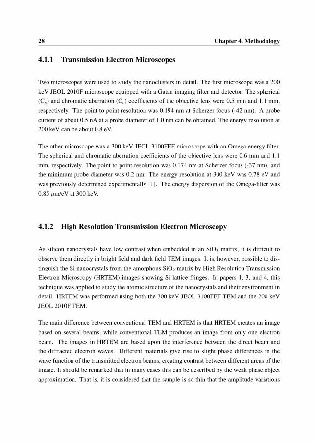
Plotting the expression y = n/u2 as a function of x = u2 yields a hyperbola for every fixed n, andthe curves that were used in paper 1 are presented in Figure 4.2. Every distance u from the centralbeam to a maximum and minimum of sin2 χ(u) in the experimental optical diffractograms shouldthen satisfy the same linear relationship between x = u2 and y = n/u2 with slope a = Csλ
3, butwith different n.
It is unknown to which n a given distance u corresponds. One therefore draws a point on everyhyperbola, keeping in mind that only one of these represents our data. Repeating this for everydistance u, one arrives at a sequence of points for any u. As consecutive u correspond to con-secutive n, fixing an n for the first u determines a sequence of points. One of these sequencesshould lie on the line given by Equation 4.4, and the sequence whose best fit has minimal erroris the most likely candidate. The value b = 2λΔf was predicted by choosing this line.
The two straight lines in Figure 4.2 were calculated for two different HRTEM images in paper1 according to the above process. The defocus Δf was then determined by the intersectionb = 2λΔf of the straight line with the y-axis. Unfortunately, the measurements of the maximaand minima in the diffractograms have large standard deviations, yielding an accuracy of ±10
nm in determining the Δf .
4.1. Transmission Electron Microscopy 33
Figure 4.2: A plot of n/u2 as a function of u2. The plot was used for finding the focus of the HRTEMimages in paper 1. The image in the bottom right corner shows a diffractogram of HRTEM image no.10 and a diffraction pattern from the Si-substrate in the same sample.
HRTEM images of small unit cells may appear periodic with focus (Δf ). The Fourier imageperiod is the period for which the first and last HRTEM images are identical. The difference infocus of such images is given by Equation 4.5. The Fourier image period of HRTEM images canbe computed from equation 4.5, for the strongest reflection uhkl inside the objective aperture [7].
Δf =2
λu2hkl
(4.5)
4.1.3 Energy Dispersive Spectroscopy
Energy Dispersive Spectroscopy (EDS) is an analytic technique used for elemental analysis andchemical characterization. In papers 3 and 4, this technique was applied to determine the compo-sition in different layers in the samples. Quantitative EDS measurements were carried out usinga 200 keV JEOL 2010F TEM with a NORAN system.
The EDS technique is based on the following process, depicted in Figure 4.3. Exposing thesample to an electron beam will cause some electrons to get kicked out of their shell, creating anelectron core hole. In an attempt to minimize the energy of the atom, outer shell electrons willtumble down to fill these holes, emitting a photon in the process. Such high energy photons arecalled X-rays. The energy is equal to the difference in the energy before and after emitting the
34 Chapter 4. Methodology
Figure 4.3: The EDS process.
photon. As such energy differences are characteristics of the elements, measuring the energy ofthe photons can be used to identify the elements present in the sample.
Technically, the emitted X-rays are detected and measured by a detector consisting of a Li dopedSi crystal cooled to liquid nitrogen temperature.
The intensities of the peaks corresponding to the characteristic energies of the elements were usedto determine the presence of different elements in the samples and to calculate the compositionof the materials. According to Cliff and Lorimer [8], if Ii and Ij are the intensities correspondingto two elements i and j, the ratio of their compositions Ci and Cj is given by
Ci
Cj
= kij · Ii
Ij
(4.6)
The kij factors are called the Cliff-Lorimer k-factors. These vary from one detector to another,and they are independent of the specimen thickness, as long as the specimen is thin. In a thickspecimen both the k-factor and the intensities of the X-rays are affected by absorption, fluores-cence and channelling effects in the specimen [3, 4].
4.1. Transmission Electron Microscopy 35
4.1.4 Electron Energy Loss Spectroscopy
Electron Energy Loss Spectroscopy (EELS) is a spectroscopy technique used to study the compo-sition and electronic structure of materials. In paper 2, EELS was applied to study the plasmonenergies of Si and SiO2 and to determine the composition and electronic structure of the nan-oclusters. Electron energy loss spectra were acquired with the JEOL 2010F microscope operatedat 197 keV and equipped with a Gatan imaging filter and detector.
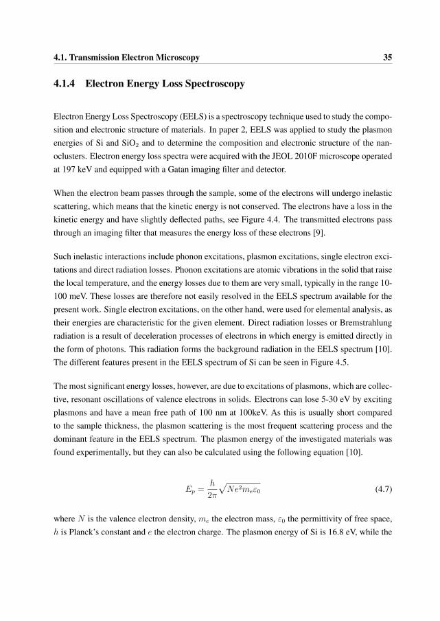
When the electron beam passes through the sample, some of the electrons will undergo inelasticscattering, which means that the kinetic energy is not conserved. The electrons have a loss in thekinetic energy and have slightly deflected paths, see Figure 4.4. The transmitted electrons passthrough an imaging filter that measures the energy loss of these electrons [9].
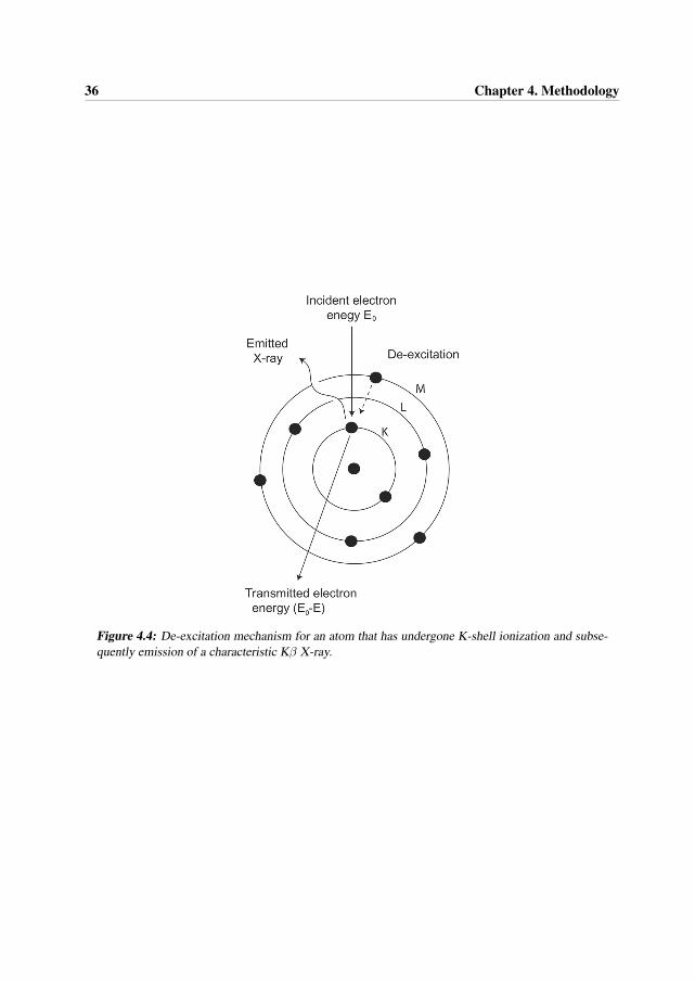
Such inelastic interactions include phonon excitations, plasmon excitations, single electron exci-tations and direct radiation losses. Phonon excitations are atomic vibrations in the solid that raisethe local temperature, and the energy losses due to them are very small, typically in the range 10-100 meV. These losses are therefore not easily resolved in the EELS spectrum available for thepresent work. Single electron excitations, on the other hand, were used for elemental analysis, astheir energies are characteristic for the given element. Direct radiation losses or Bremstrahlungradiation is a result of deceleration processes of electrons in which energy is emitted directly inthe form of photons. This radiation forms the background radiation in the EELS spectrum [10].The different features present in the EELS spectrum of Si can be seen in Figure 4.5.
The most significant energy losses, however, are due to excitations of plasmons, which are collec-tive, resonant oscillations of valence electrons in solids. Electrons can lose 5-30 eV by excitingplasmons and have a mean free path of 100 nm at 100keV. As this is usually short comparedto the sample thickness, the plasmon scattering is the most frequent scattering process and thedominant feature in the EELS spectrum. The plasmon energy of the investigated materials wasfound experimentally, but they can also be calculated using the following equation [10].
Ep =h
2π
√Ne2meε0 (4.7)
where N is the valence electron density, me the electron mass, ε0 the permittivity of free space,h is Planck’s constant and e the electron charge. The plasmon energy of Si is 16.8 eV, while the
36 Chapter 4. Methodology
Figure 4.4: De-excitation mechanism for an atom that has undergone K-shell ionization and subse-quently emission of a characteristic Kβ X-ray.
4.1. Transmission Electron Microscopy 37
Figure 4.5: An EELS spectrum of Si showing the different peaks present, with an energy dispersionof about 0.8 eV. The inserted EELS image has a lower count on the y-axis (102).
corresponding value of SiO2 is 23 eV. This is a 6.2 eV energy difference, which is large enoughfor the two peaks to be separated in the EELS spectrum. Shifts in the Si plasmon peak werestudied in papers 1 and 2. This shift can be due to an increase in electron density or oxygenconcentration, and this affects the shape of the plasmon peak.
4.1.5 Energy Filtered Transmission Electron Microscopy - Spectral Imag-ing
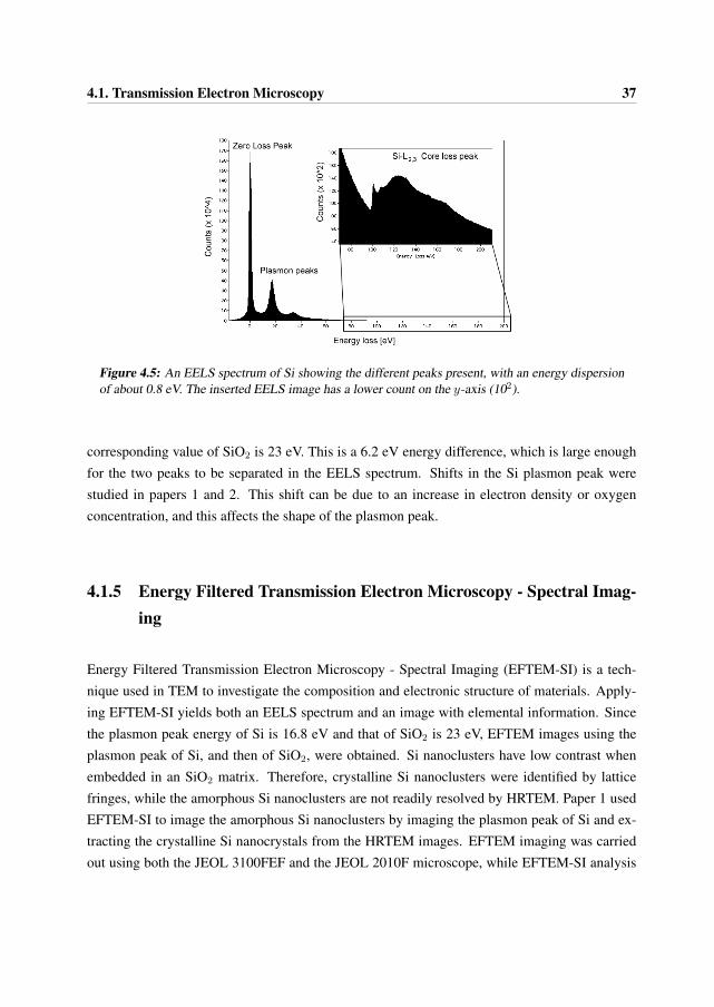
Energy Filtered Transmission Electron Microscopy - Spectral Imaging (EFTEM-SI) is a tech-nique used in TEM to investigate the composition and electronic structure of materials. Apply-ing EFTEM-SI yields both an EELS spectrum and an image with elemental information. Sincethe plasmon peak energy of Si is 16.8 eV and that of SiO2 is 23 eV, EFTEM images using theplasmon peak of Si, and then of SiO2, were obtained. Si nanoclusters have low contrast whenembedded in an SiO2 matrix. Therefore, crystalline Si nanoclusters were identified by latticefringes, while the amorphous Si nanoclusters are not readily resolved by HRTEM. Paper 1 usedEFTEM-SI to image the amorphous Si nanoclusters by imaging the plasmon peak of Si and ex-tracting the crystalline Si nanocrystals from the HRTEM images. EFTEM imaging was carriedout using both the JEOL 3100FEF and the JEOL 2010F microscope, while EFTEM-SI analysis
38 Chapter 4. Methodology
Figure 4.6: The figure exhibits how an EFTEM-SI image is made up of an EELS spectrum in eachpoint in the 2-dimensional image. The image at the top is made by the plasmon peak of Si, which liesat 16.8 eV. (Adapted from Ahn[11].)
was performed using only the 300 keV JEOL 3100FEF TEM with an Omega imaging filter.
EFTEM images can be created from all the electrons with a particular kinetic energy. The otherelectrons are excluded by the presence of a narrow slit, and increasing the slit width will allowmore electrons to be included in the image. By combining such EFTEM images for different en-ergies in a certain energy range, one can create an EFTEM-SI file containing all the informationof the individual EFTEM images in addition to the EELS spectra, see Figure 4.6.
4.1.6 Scanning Transmission Electron Microscopy
Scanning Transmission Electron Microscopy (STEM) is a TEM technique in which a focusedelectron beam is scanned over the sample. The STEM microscope has both a Bright Field (BF)detector and a High Angle Annular Detector (HAAD). With an HAAD, images with high Z-contrast can be obtained. In paper 4, STEM was used to image the Er distribution in the SiO2-Silayers and the microscopy was performed using a 300 keV JEOL 3100FEF TEM equipped withan Omega imaging filter and a JEOL STEM detector.
The technique is based upon the fact that the Z-contrast is directly related to the atomic number(Z), making it possible to contrast materials with different atomic numbers. Atoms with a higher
4.2. X-ray Photoelectron Spectroscopy 39
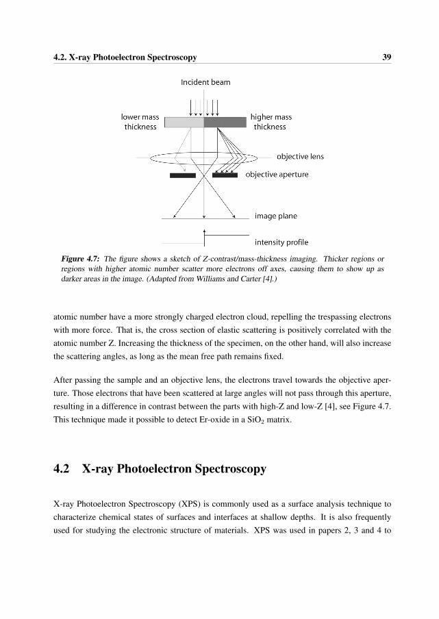
Figure 4.7: The figure shows a sketch of Z-contrast/mass-thickness imaging. Thicker regions orregions with higher atomic number scatter more electrons off axes, causing them to show up asdarker areas in the image. (Adapted from Williams and Carter [4].)
atomic number have a more strongly charged electron cloud, repelling the trespassing electronswith more force. That is, the cross section of elastic scattering is positively correlated with theatomic number Z. Increasing the thickness of the specimen, on the other hand, will also increasethe scattering angles, as long as the mean free path remains fixed.
After passing the sample and an objective lens, the electrons travel towards the objective aper-ture. Those electrons that have been scattered at large angles will not pass through this aperture,resulting in a difference in contrast between the parts with high-Z and low-Z [4], see Figure 4.7.This technique made it possible to detect Er-oxide in a SiO2 matrix.
4.2 X-ray Photoelectron Spectroscopy
X-ray Photoelectron Spectroscopy (XPS) is commonly used as a surface analysis technique tocharacterize chemical states of surfaces and interfaces at shallow depths. It is also frequentlyused for studying the electronic structure of materials. XPS was used in papers 2, 3 and 4 to
40 Chapter 4. Methodology
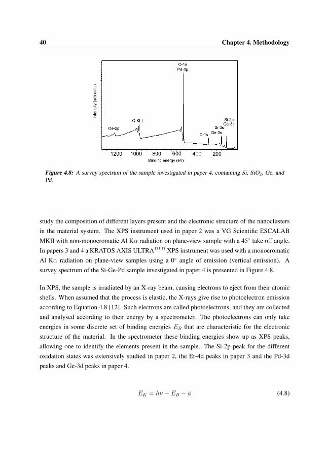
Figure 4.8: A survey spectrum of the sample investigated in paper 4, containing Si, SiO2, Ge, andPd.
study the composition of different layers present and the electronic structure of the nanoclustersin the material system. The XPS instrument used in paper 2 was a VG Scientific ESCALABMKII with non-monocromatic Al Kα radiation on plane-view sample with a 45◦ take off angle.In papers 3 and 4 a KRATOS AXIS ULTRADLD XPS instrument was used with a monocromaticAl Kα radiation on plane-view samples using a 0◦ angle of emission (vertical emission). Asurvey spectrum of the Si-Ge-Pd sample investigated in paper 4 is presented in Figure 4.8.
In XPS, the sample is irradiated by an X-ray beam, causing electrons to eject from their atomicshells. When assumed that the process is elastic, the X-rays give rise to photoelectron emissionaccording to Equation 4.8 [12]. Such electrons are called photoelectrons, and they are collectedand analysed according to their energy by a spectrometer. The photoelectrons can only takeenergies in some discrete set of binding energies EB that are characteristic for the electronicstructure of the material. In the spectrometer these binding energies show up as XPS peaks,allowing one to identify the elements present in the sample. The Si-2p peak for the differentoxidation states was extensively studied in paper 2, the Er-4d peaks in paper 3 and the Pd-3dpeaks and Ge-3d peaks in paper 4.
EK = hν − EB − φ (4.8)
4.2. X-ray Photoelectron Spectroscopy 41
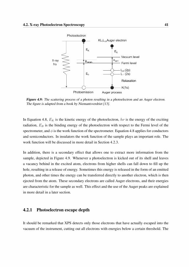
Figure 4.9: The scattering process of a photon resulting in a photoelectron and an Auger electron.The figure is adapted from a book by Niemantsverdriet [13].
In Equation 4.8, EK is the kinetic energy of the photoelectron, hν is the energy of the excitingradiation, EB is the binding energy of the photoelectron with respect to the Fermi level of thespectrometer, and φ is the work function of the spectrometer. Equation 4.8 applies for conductorsand semiconductors. In insulators the work function of the sample plays an important role. Thework function will be discussed in more detail in Section 4.2.3.
In addition, there is a secondary effect that allows one to extract more information from thesample, depicted in Figure 4.9. Whenever a photoelectron is kicked out of its shell and leavesa vacancy behind in the excited atom, electrons from higher shells can fall down to fill up thehole, resulting in a release of energy. Sometimes this energy is released in the form of an emittedphoton, and other times the energy can be transferred directly to another electron, which is thenejected from the atom. These secondary electrons are called Auger electrons, and their energiesare characteristic for the sample as well. This effect and the use of the Auger peaks are explainedin more detail in a later section.
4.2.1 Photoelectron escape depth
It should be remarked that XPS detects only those electrons that have actually escaped into thevacuum of the instrument, cutting out all electrons with energies below a certain threshold. The
42 Chapter 4. Methodology
probability of finding a particle at depth z into the material is calculated by Lambert-Beer’s law
P (x) = e−z/λ (4.9)
where λ is the absorption length, which is the distance into the material corresponding to thesituation of the probability that a particle has not been absorbed has dropped to 1/e. The intensityof a beam of light measured before and after interaction with a sample is compared [14], and cantherefore be described by as
I = I0e−μx (4.10)
where I0 is the intensity of the incoming X-rays, x is the sample thickness and μ is the linearabsorption coefficient. The flux of electrons emitted at a depth z and detected at a polar angleθ (see Figure 4.10) from the surface normal will be reduced by inelastic scattering according tothe Beer-Lambert relationship [15] [16]
I(z, φ) = I0e−z/(λ sin φ) (4.11)
where I(z, φ) is the intensity from the atoms at a depth z, I0 is the intensity from the surfaceatoms, φ is the electron take-off angle (φ = 90 − θ, where θ is angle of emission), and λ isthe mean free path. In the case of exponential decay, if the absorption length is λAL, then for atake-off angle φ to the surface, the escape depth d is equal to λAL sin φ. Commonly 3d (95 %detection) is taken to be the “sampling depth”, which is equal to 3dλAL sin φ [16].
The mean free path of the elements of interest in this study were found using the NIST StandardReference Database 71 [17]. The inelastic mean free path of a selected element in the databasewas determined by optical data and a theoretical model developed by Tanuma, Powell, and Penn[18]. This model is a modified form of the Bethe equation [19] for inelastic electron scatteringin matter and is dependent of the atomic weight, bulk density, and number of valence electronsper atom, see Equation 4.12 [18].
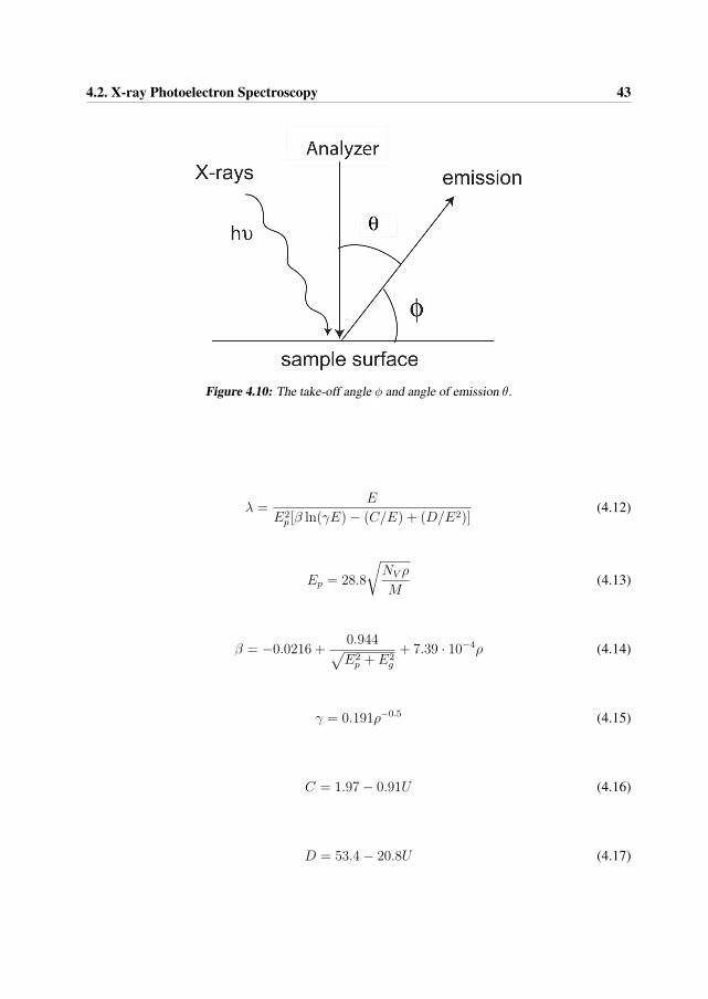
4.2. X-ray Photoelectron Spectroscopy 43
Figure 4.10: The take-off angle φ and angle of emission θ.
λ =E
E2p [β ln(γE) − (C/E) + (D/E2)]
(4.12)
Ep = 28.8
√NV ρ
M(4.13)
β = −0.0216 +0.944√E2
p + E2g
+ 7.39 · 10−4ρ (4.14)
γ = 0.191ρ−0.5 (4.15)
C = 1.97 − 0.91U (4.16)
D = 53.4 − 20.8U (4.17)
44 Chapter 4. Methodology
U =Nvρ
M=
E2p
829.4(4.18)
where E is the electron energy (in eV), Ep is the free-electron plasmon energy (in eV), Nv isthe number of valence electrons per atom, ρ is the material density (in g/cm3), M the atomicweight, and Eg the band-gap energy (in eV). The symbols γ, β, C, and D represent additionalparameters.
4.2.2 The binding energy
The binding energy for a particular core level in a molecule (first approximation) can be ex-pressed as Equation 4.19 [20]. This equation shows that the binding energies increase withincreasing positive charge.
EB = Kq + L (4.19)
where K and L are empirical constants and q is the charge on the ion in the particular moleculerelative to the neutral atom. Thus L is the binding energy of the electron in question in the freeneutral atom.
In a molecule the electron experiences not only the charge of that atom, but will experience, apartfrom intra atomic relaxation, also extra atomic relaxation effects and potential charges from otheratoms in the molecule. The relaxation energy R (intra- and extra atomic), is the energy gainedwhen the electrons in the molecule respond to the photohole produced by the photoemissionprocess. The relaxation energy is negative because it decreases the binding energy. The potentialenergy V produced by all other atoms in the molecule expresses the field produced by the chargesof the other atoms. This leads to Equation 4.20.
EB = Kq + V + L − R (4.20)
4.2. X-ray Photoelectron Spectroscopy 45
4.2.3 The chemical shift
Shifts in the binding energy EB were studied in paper 2, 3, and 4. Binding energy shifts areinfluenced by both initial (prior to photoemission) and final (after photoemission and Augeremission) state effects.
The chemical shift is the peak shift between two different chemical environments and is definedas the binding energy difference (ΔEB) between atoms bonded to different chemical species,e.g. elemental Si and SiO2 (EB Si4+ - EB Si0). In pure Si, the 3p electrons form a band, and theirwave function is therefore only partly at the site of a particular Si atom. However, in SiO2 eachSi atom donates its 3p electrons into the 2p shell of oxygen such that a closed 2p6 configurationis obtained. Thus in SiO2 the Si 3p electrons have no part of their wave functions near the Siatom. The 2p electrons in SiO2 feel a stronger Coulomb interaction than in pure Si, where theSi nucleus is shielded from the 2p shell through the 3p valence electrons. Therefore the bindingenergy of Si 2p level is larger in SiO2 than in pure Si, and a chemical shift between the twocompounds is observed.
This shift was used to help identify the different oxidation states of Si in paper 2, of Er in paper3, and Pd and Ge in paper 4. However, determination of chemical shifts depends on reliable mea-surements of XPS peak positions, which in turn are sensitive to energy referencing issues. It isalso difficult to compare samples that have been investigated with different spectrometers and/orexperimental setups. When examining samples that are partially (semi)conducting and partiallyinsulating, the sample surface tends to charge (non uniformly) when exposed to the X-ray beam.The non uniform charging creates different shifts in the XPS peaks, and this is called differentialcharging. Since the samples investigated in this work contained semiconducting nanocrystals inan insulating oxide, charging effects influenced the binding energies and therefore the chemicalshifts. In papers 3 and 4 we used monochromatic radiation. Charging phenomena are more in-tense when monochromatic X-rays are used. However, the experiments were run using a chargeneutralization system based on low kinetic energy electrons “flooding” the sample surface. Whenachromatic radiation is used (e.g. with a dual Al/Mg Kα anode) as in paper 2, charge compen-sation occurs to some extent by secondary electrons generated inside the spectrometer by theachromatic beam. Differential charging phenomena were studied in paper 2.
If final state relaxation effects are not taken into account, the core level binding energy differencebetween two compounds A and B is given by Equation 4.21 (after Equation 4.20).
46 Chapter 4. Methodology
ΔEB(A,B) = K(qA − qB) + (V A − V B) (4.21)
The first term (KΔq) describes the difference in electron-electron interaction between the coreorbital and the valence charges. It expresses the changes in the number of valence electrons inthe atom. K is the Coulomb interaction between the valence and core electrons. The secondterm (ΔV ) represents the interaction of the atom to be photoionized with the rest of the crystaland can be described by Equation 4.22 [21]
VA →N∑
c�=A
qc
rcA
(4.22)
where qc is the effective charge on the set of atoms (except A) in the environment of A and thercA are the appropriate inter-atomic distances. In molecular solids the atoms A bonded to atomB, but in ionic solids the summation extends over the whole lattice. The rcA terms in Equation4.22 can be extracted from the lattice measurements or spectroscopic determinations, and onlythe effective charges qc can be determined by any argument of the ionic character of the bond.This term is directly related to the Madelung energy of the solid and for this reason V is oftenreferred to as the Madelung potential. The Madelung energy is described by Equation 4.23.
E = −Z2e2M
4πε0r0
(4.23)
where M is the Madelung constant, which is representative of the distance of the ions from oneanother in a specific type of crystal. It is described as the energy of a single ion, dependingon how close it is to other ions and charges, and is a modified electron energy. 1/(4πε0) is theCoulomb force constant or the electrostatic constant equal to 8.987 · 109 Nm2C−2.
The two terms KΔq and ΔV (in Equation 4.21) are initial state parameters and reflect changes inthe atomic potential arising from changes in valence electron charge and Coulomb interactionsat the emission site. In addition to these two terms, the chemical potential (Δμ) or the workfunction (ϕ) are often added to the equation as energy referencing parameters [22]. The workfunction and the chemical potential are discussed in more detail in the next section. The chemical
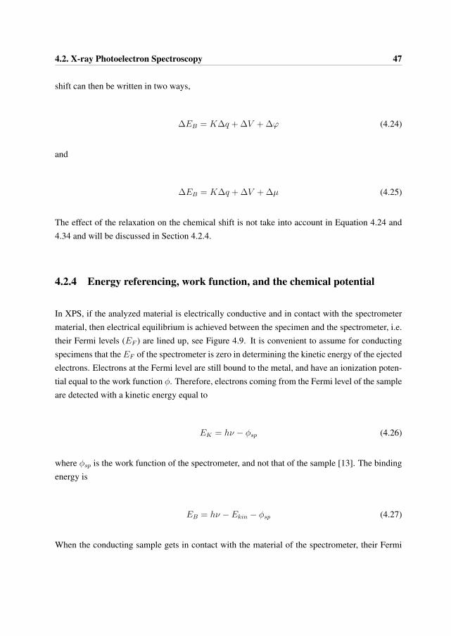
4.2. X-ray Photoelectron Spectroscopy 47
shift can then be written in two ways,
ΔEB = KΔq + ΔV + Δϕ (4.24)
and
ΔEB = KΔq + ΔV + Δμ (4.25)
The effect of the relaxation on the chemical shift is not take into account in Equation 4.24 and4.34 and will be discussed in Section 4.2.4.
4.2.4 Energy referencing, work function, and the chemical potential
In XPS, if the analyzed material is electrically conductive and in contact with the spectrometermaterial, then electrical equilibrium is achieved between the specimen and the spectrometer, i.e.their Fermi levels (EF ) are lined up, see Figure 4.9. It is convenient to assume for conductingspecimens that the EF of the spectrometer is zero in determining the kinetic energy of the ejectedelectrons. Electrons at the Fermi level are still bound to the metal, and have an ionization poten-tial equal to the work function φ. Therefore, electrons coming from the Fermi level of the sampleare detected with a kinetic energy equal to
EK = hν − φsp (4.26)
where φsp is the work function of the spectrometer, and not that of the sample [13]. The bindingenergy is
EB = hν − Ekin − φsp (4.27)
When the conducting sample gets in contact with the material of the spectrometer, their Fermi
48 Chapter 4. Methodology
levels are the same, but their work functions differ. In order to remove an electron at the Fermilevel from the sample, energy costs equal to φ, the work function of the sample is used. Electronswill then pass from the metal with low φ to the metal with high φ. The electron that is liberatedfrom the sample is now at the potential just outside the sample (“local vacuum level”), but notyet at the potential of the spectrometer, which in this set-up defines the vacuum level. While en
route to the analyzer, the electron is accelerated or decelerated by the work function difference,which is the contact potential between the sample and the spectrometer [13] until a potentialdifference φ0 −φsp is reached, where φ0 is the work function of the sample. Since vacuum levelsare different, it is necessary to add φ0 to EB in order to obtain ionization energies relative to thevacuum level.
Eion = Eb + φ0 (4.28)
So Equation 4.27 becomes
Eion = hν − Ekin + (φ0 − φsp) (4.29)
If the specimen is a semiconductor (or insulator) then the Fermi levels are not equal. In addition,the electrical potential of the specimen and spectrometer are not equal (exceptions occur whenthin insulating films are deposited on conducting substrates, then the potentials of the film andsubstrate even out). In this case
Eb = hν − Ekin − φsp ± Ediff (4.30)
where Ediff is the difference between the potentials of the surface of the sample and the spec-trometer. When we apply charge compensation, we flood electrons on to the sample surface sothat the vacuum level of the sample now will be at the same level with the EF of the spectrometer.Then
EB = hν − EK + Fe − φsample (4.31)
4.2. X-ray Photoelectron Spectroscopy 49
The work function can also be dependent on the chemical potential
φsp = Δφmet. − μ (4.32)
where Δφmet. is the rise in mean electrostatic potential across the metal surface, and μ is thebulk chemical potential of the electrons relative to the mean electrostatic potential in the metalinterior.
The chemical potential governs the flow of particles between the system, just as the temperaturegoverns the flow of energy [23].This means that when two systems with a single chemical speciesare at the same temperature and have the same value of the chemical potential, there will be nonet flow and no net energy flow between them [23]. The chemical potential can be described as
μ =
(∂U
∂Ni
)S,V,Nj �=i
(4.33)
where U is the internal energy of the system, V is the volume, S is the entropy, and the numberof particles of each specimen is N1, . . . , Nn. The subscripts emphasize that the entropy, volume,and the other particle numbers are to be kept constant.
By taking into account final state relaxation effects, Equation 4.21 can be expressed as below,including the extra atomic relaxation energy.
ΔEB = KΔq + ΔV + Δϕ − ΔR (4.34)
If the experiment is performed in the same instrument, then the contribution of φsp in Equations4.32 and 4.34 is zero. Assuming that φsample is the same in different chemical environments,Equation 4.34 can be simplified to
ΔEB = KΔq + ΔV − ΔR (4.35)
50 Chapter 4. Methodology
The shift in kinetic energy can also be expressed in this matter, but has negative potential andpositive relaxation energy terms.
ΔEK = −KΔq − ΔV − Δϕ + 3ΔR (4.36)
4.2.5 Screening
In the previous section we refered only to initial state effects in the binding energy shifts. How-ever, binding energies are also influenced by changes in the extra atomic relaxation energy as-sociated with changes in core hole screening. Since the chemical shift contains both initial andfinal state contributions, it makes it more difficult to determine the cause of the shift. In papers2, 3 and 4, a core shift was found in the XPS peaks, and screening was discussed as a possibleeffect. The screening can be expressed by Equation 4.37. Two charges q1 and q2 separated by adistance r have a Coulomb interaction energy of
U(r) =keq1q2
r(4.37)
where ke = 1/(4πε0) = 8.99 · 109 Nm2/C2 and ε0 is the permittivity in vacuum or the electricconstant. This equation expresses long range interactions because of its slow power-law decay.
The materials studied in this work have a high dielectric constant, 11.9 for Si, 16 for Ge, 13for Er2O3, and 3.9 for SiO2. The screening in a dielectric material can be described by theCoulomb interaction reduced in strength by the dielectric constant e, as seen in Equation 4.38.The reduction in Coulomb interaction is due to polarization of the particles in the dielectricmaterial. Induced or permanent dipoles around a free charge will be oriented so as to terminatesome of the field lines coming from the free charge. This effect is called the dielectric screening.
U(r) =keq1q2
er(4.38)
In papers 3 and 4, a core hole shift in the binding energy of Er-oxide and Pd was found. Inorder to determine the screening effect of the surrounding matrix on the clusters, the universal
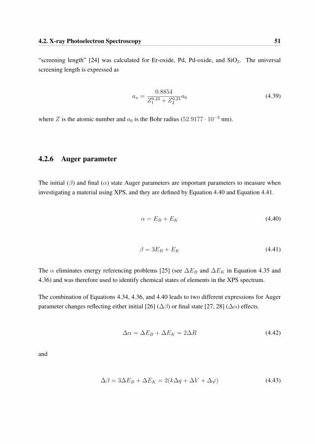
4.2. X-ray Photoelectron Spectroscopy 51
“screening length” [24] was calculated for Er-oxide, Pd, Pd-oxide, and SiO2. The universalscreening length is expressed as
au =0.8854
Z0.231 + Z0.23
2
a0 (4.39)
where Z is the atomic number and a0 is the Bohr radius (52.9177 · 10−3 nm).
4.2.6 Auger parameter
The initial (β) and final (α) state Auger parameters are important parameters to measure wheninvestigating a material using XPS, and they are defined by Equation 4.40 and Equation 4.41.
α = EB + EK (4.40)
β = 3EB + EK (4.41)
The α eliminates energy referencing problems [25] (see ΔEB and ΔEK in Equation 4.35 and4.36) and was therefore used to identify chemical states of elements in the XPS spectrum.
The combination of Equations 4.34, 4.36, and 4.40 leads to two different expressions for Augerparameter changes reflecting either initial [26] (Δβ) or final state [27, 28] (Δα) effects.
Δα = ΔEB + ΔEK = 2ΔR (4.42)
and
Δβ = 3ΔEB + ΔEK = 2(kΔq + ΔV + Δϕ) (4.43)
52 Chapter 4. Methodology
The final and initial state Auger parameter values calculated for the different samples investigatedin paper 2 showed large deviations. Changes in the initial state Auger parameter showed thatthe shift in binding energy was mostly due to initial state effects, where the Si0 sites in thenanoclusters had a negative charge, while the Si0 sites in the supersaturated silica (with Si) had apositive charge.
Screening, being a final state effect, was also an important factor to consider. The final stateAuger parameter is a measure of the screening efficiency in the presence of core holes and isfree of any referencing problems [29, 30, 31]. Equation 4.42 shows how the final state Augerparameter provides an estimate of the relaxation/screening energy in the presence of core holes.It shows that a high α-value indicates higher relaxation energy or improved screening efficiency.It should be noted that Equation 4.42 is not reliable for transition metals, due to intra atomiccharge transfer [32].
Due to the triple weighting of the binding energy EB in its definition (see Equation 4.43), theinitial state Auger parameter is not completely independent of energy referencing. Therefore, β
can be potentially influenced by work function differences and charging effects. The initial stateAuger parameter β reflects nevertheless changes in the population of valence electrons, as wellas changes in the Madelung potential.
In order to visualize the initial and final state Auger parameter changes in paper 2, a Wagnerdiagram was plotted. A Wagner diagram [33] is made by plotting the binding energy of thephotoelectron peak against the kinetic energy of the Auger electron peak. The Auger kineticenergy is on the ordinate and the photoelectron binding energy is on the abscissa oriented in thenegative direction [25, 33]. The Wagner diagram plotted in paper 2 is shown in Figure 4.11.The Auger parameters are expressed by the linear relationship between EK (Auger peak) andEB (photoemission peak), and they lie on the straight lines with slope +1 (final state α) and +3(initial state β). This means that for each line, every point lying on this line has the same Augerparameter value. This diagram helps to visualize changes in the relative Auger parameter values.
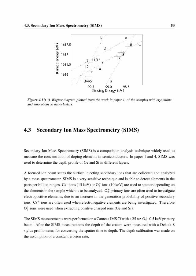
4.3. Secondary Ion Mass Spectrometry (SIMS) 53
Figure 4.11: A Wagner diagram plotted from the work in paper 1, of the samples with crystallineand amorphous Si nanoclusters.
4.3 Secondary Ion Mass Spectrometry (SIMS)
Secondary Ion Mass Spectrometry (SIMS) is a composition analysis technique widely used tomeasure the concentration of doping elements in semiconductors. In paper 1 and 4, SIMS wasused to determine the depth profile of Ge and Si in different layers.
A focused ion beam scans the surface, ejecting secondary ions that are collected and analyzedby a mass spectrometer. SIMS is a very sensitive technique and is able to detect elements in theparts per billion ranges. Cs+ ions (15 keV) or O+
2 ions (10 keV) are used to sputter depending onthe elements in the sample which is to be analyzed. O+
2 primary ions are often used to investigateelectropositive elements, due to an increase in the generation probability of positive secondaryions. Cs+ ions are often used when electronegative elements are being investigated. ThereforeO+
2 ions were used when extracting positive charged ions (Ge and Si).
The SIMS measurements were performed on a Cameca IMS 7f with a 25 nA O+2 , 0.5 keV primary
beam. After the SIMS measurements the depth of the craters were measured with a Dektak 8stylus profilometer, for converting the sputter time to depth. The depth calibration was made onthe assumption of a constant erosion rate.
54 Chapter 4. Methodology
References
[1] Y. BANDO, M. MITOME, D. GOLBERG, Y. KITAMI, K. KURASHIMA, T. KANEYAMA,Y. OKURA, and M. NARUSE, Jpn. J. Appl. Phys. 40, L 1193 (2001).
[2] HTTP://WWW.MAXSIDOROV.COM/CTFEXPLORER/WEBHELP/BACKGROUND.HTM.
[3] A. OLSEN, The Theory and Practice of Analytical Electron Microscopy in Material Sci-
ence, University of Oslo, 2002.
[4] D. B. WILLIAMS and C. B. CARTER, Transmission Electron Microscopy: A text book in
Material Science, Plenum press, New York, 1996.
[5] J. S. SPENCE, Experimental High-Resolution Electron Microscopy, Oxford UniversityPress, 2 edition, 1988.
[6] F. THON, Electron microscopy in Material Science, pp. 570–590, New York; Academicpress, u. valdre and a. zichichi edition, 1971.
[7] A. OLSEN and J. SPENCE, Phil. Mag. A 43, 945 (1981).
[8] G. CLIFF and G. LORIMER, J. of Microscopy 103, 203 (1975).
[9] R. EGERTON, Electron Energy Loss Spectroscopy in the Electron Microscope, Plenumpress, New York, 1986.
[10] R. BRYDSON, Electron Energy Loss Spectroscopy, BIOS Scientific Publishers Limited,2001.
[11] C. C. AHN, Transmission Electron Energy Loss Spectrometry in Materials Science and
EELS ATLAS, WILEY-VCH, 2 edition, 2004.
[12] D. BRIGGS and M.P.SEAH, Practical Surface Analysis, volume 1, John Wiley ANd SonsAND Salle and Sauerlander, second edition, 1990.
[13] A. DUPASQUIER and A. P. MILLS, Positron Spectroscopy of Solids: Proceedings of the
International School of Physics ”Enrico Fermi”, Varenna on Lake Como, Villa Monastero,
6-16 July 1993, IOS Press, 1993.
4.3. References 55
[14] G. AKGUL, F. AKSOY, Y. UFUKTEPE, and J. LUNING, Sol. Stat. Commun. 149, 384(2009).
[15] F. BRUNO, L. FLOREANO, A. VERDINI, D. CVETKO, R. GOTTER, A. MORGANTE,M. CANEPA, and S. TERRENI, J. Electron. Spectrosc. Relat. Phenom. 127, 85 (2002).
[16] D. BRIGGS, Surface analysis of polymers by XPS and static SIMS, Cambridge UniversityPress, 1998.
[17] C. J. POWELL and A. JABLONSKI, NIST Electron Inelastic-Mean-Free-Path Database 71,National Institute of Standards and Technology, 2000.
[18] S. TANUMA, C. POWELL, and D. PENN, Surf. Interface Anal. 17, 911 (1991).
[19] H. BETHE, Ann. Phys. 5, 325 (1930).
[20] S. HUFNER, Photoelectron Spectroscopy: Principles and Applications, Springer, 2003.
[21] T. L. BARR, Modern ESCA: The Principles and Practice of X-ray Photoelectron Spec-
troscopy, CRC Press, 1994.
[22] N. HARIMA, J. MATSUNO, A. FUJIMORI, Y. Y. ONOSE, TAGUCHI, and Y. TOKURA,Phys. Rev. B 64, 220507 (2001).
[23] C. KITTEL and H. KROEMER, Thermal Physics, FREEMAN, 2 edition, 1980.
[24] S. TIAN, J. Appl. Phys. 93, 5893 (2003).
[25] C. D. WAGNER, Anal. Chem. 47, 1201 (1975).
[26] J. A. EVANS, A. LAINE, P. WEIGHMAN, J. A. D. MATTHEW, D. A. WOOLF, D. I.WESTWOOD, and R. H. WILLIAMS, Phys. Rev. B 46, 1513 (1992).
[27] S. W. GAARENSTROM and N. WINOGRAD, J. Chem. Phys. 67, 3500 (1977).
[28] T. D. THOMAS and P. WEIGHTMAN, Phys. Rev. B 33, 5406 (1986).
[29] S. C. LAWRENCE, J. Phys. Chem. 55, 95 (1971).
[30] C. G. H. WALKER, G. B. S. A. MOTRON, J. A. D. MATTHEW, and F. N. YOUSIF, J.
Electron. Spectrosc. Relat. Phenom. 70, 73 (1994).

56 Chapter 4. Methodology
[31] J. A. D. MATTHEW, S. A. MORTON, C. G. H. WALKER, and G. BEAMSON, J. Phys. D
28, 1702 (1995).
[32] G. KLEIMAN and R. LANDERS, J. Electron. Spectrosc. Relat. Phenom. 76, 319 (1995).
[33] G. MORETTI, J. Electron. Spectrosc. Relat. Phenom. 95, 95 (1998).
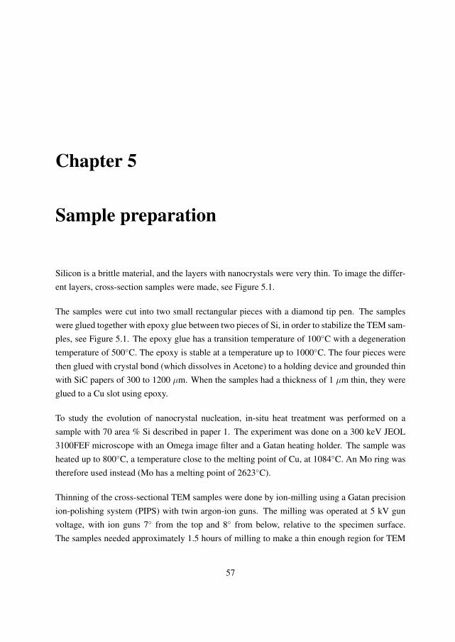
Chapter 5
Sample preparation
Silicon is a brittle material, and the layers with nanocrystals were very thin. To image the differ-ent layers, cross-section samples were made, see Figure 5.1.
The samples were cut into two small rectangular pieces with a diamond tip pen. The sampleswere glued together with epoxy glue between two pieces of Si, in order to stabilize the TEM sam-ples, see Figure 5.1. The epoxy glue has a transition temperature of 100◦C with a degenerationtemperature of 500◦C. The epoxy is stable at a temperature up to 1000◦C. The four pieces werethen glued with crystal bond (which dissolves in Acetone) to a holding device and grounded thinwith SiC papers of 300 to 1200 μm. When the samples had a thickness of 1 μm thin, they wereglued to a Cu slot using epoxy.
To study the evolution of nanocrystal nucleation, in-situ heat treatment was performed on asample with 70 area % Si described in paper 1. The experiment was done on a 300 keV JEOL3100FEF microscope with an Omega image filter and a Gatan heating holder. The sample washeated up to 800◦C, a temperature close to the melting point of Cu, at 1084◦C. An Mo ring wastherefore used instead (Mo has a melting point of 2623◦C).
Thinning of the cross-sectional TEM samples were done by ion-milling using a Gatan precisionion-polishing system (PIPS) with twin argon-ion guns. The milling was operated at 5 kV gunvoltage, with ion guns 7◦ from the top and 8◦ from below, relative to the specimen surface.The samples needed approximately 1.5 hours of milling to make a thin enough region for TEM
57
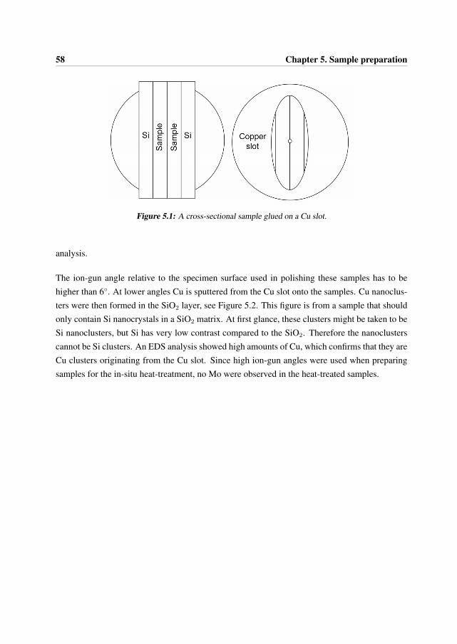
58 Chapter 5. Sample preparation
Figure 5.1: A cross-sectional sample glued on a Cu slot.
analysis.
The ion-gun angle relative to the specimen surface used in polishing these samples has to behigher than 6◦. At lower angles Cu is sputtered from the Cu slot onto the samples. Cu nanoclus-ters were then formed in the SiO2 layer, see Figure 5.2. This figure is from a sample that shouldonly contain Si nanocrystals in a SiO2 matrix. At first glance, these clusters might be taken to beSi nanoclusters, but Si has very low contrast compared to the SiO2. Therefore the nanoclusterscannot be Si clusters. An EDS analysis showed high amounts of Cu, which confirms that they areCu clusters originating from the Cu slot. Since high ion-gun angles were used when preparingsamples for the in-situ heat-treatment, no Mo were observed in the heat-treated samples.
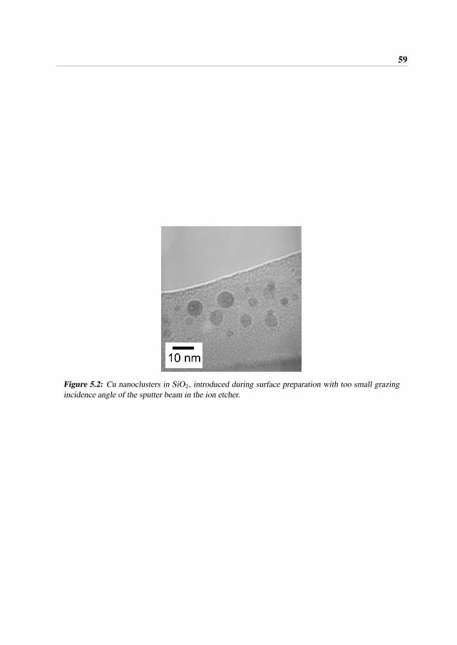
59
Figure 5.2: Cu nanoclusters in SiO2, introduced during surface preparation with too small grazingincidence angle of the sputter beam in the ion etcher.

Chapter 6
Overview of papers
This work is presented in four papers and is in cooperation with the Physical Electronics group atMINAlab, where Jeyanthinath Mayandi made the samples with Terje Finstad as his supervisor.Part of the work was also done during a four month stay at the National Institute of MaterialScience (NIMS) in Tsukuba Japan, with Masanori Mitome and Yoshio Bando. The two firstpapers have been published in Journal of Applied Physics, the third has been submitted and thelast paper will be submitted shortly as of this writing.
Paper I
In the previous chapters, the memory device stability was discussed with regards to the atomicstructure and size of the nanoclusters, nucleation, distribution, and defects. Several samplescontaining pure Si embedded in a thin SiO2 layer, heat treated at different temperatures andtimes, were studied by HRTEM, EDS, EELS, EFTEM, and SIMS. Jens Sherman Christensenran the SIMS measurements on the instrument at MINAlab.
The study revealed both amorphous and crystalline nanoclusters of Si in the amorphous SiO2
matrix. At low Si percentage (below 50 area %) only amorphous Si nanoclusters were nucle-ated in the oxide, and at higher Si concentration, crystalline nanoclusters were observed. TEMand SIMS results showed that the nanocluster nucleation occurred where maximum excess Siis the highest: in a 4 nm band, 5 nm from the Si substrate, and 4 nm from the SiO2 surface.
61
62 Chapter 6. Overview of papers
Defects (twins and stacking faults) in the nanocrystals were also found and studied in detail byHRTEM and image simulations. Both single and double twin boundaries were observed in thenanocrystals.
Paper II
As discussed in the previous sections, the atomic and electronic structure can have large effectsupon the material properties. To obtain a better understanding of the electronic structure of thenanoclusters observed in paper 1, an XPS study of the binding energy and the Auger parameterof the different samples were performed. EELS was used to study the shift in plasmon energy ofthe different samples and in order to relate it to the valence electron density.
The XPS study was under the supervision of Spyros Diplas, who ran the XPS measurements atthe instrument in Surrey England, and John F. Watts contributed with comments and discussions.
The XPS results of the amorphous and crystalline nanoclusters showed large shifts in binding en-ergy and Auger parameter. The shift in Si2p binding energy was studied by separating initial andfinal state effects using the Auger parameter. The negative charge on the Si0 sites in nanoclustersand the positive charge on the Si0 sites in the supersaturated silica, as indicated by the initial stateAuger parameter, dominated both differential charging and chemical shifts. The differences inchemical shift was attributed to initial state effects. The final state Auger parameter showed thatthe electron screening of silicon core holes in nanocrystals dispersed in SiO2 is inferior to that inpure bulk Si. This is due to the non local screening character of Si.
Paper III
In this paper samples containing Er with only small amounts of pure Si in the SiO2 matrix wereinvestigated by HRTEM, EFTEM-SI, EELS, STEM, and XPS in order to study the effect onnucleation, distribution, and composition.
Amorphous Er-oxide nanoclusters were observed. These nanoclusters nucleated as a result ofelectron beam exposure. The nanocluster evolution was studied in detail. Initially the nanoclus-ters’ growth matched the Ostwald ripening model, but eventually it stagnated at a constant nan-
63
ocluster radius of 2.4 nm. The nanocluster composition was studied by microscopy techniquesand XPS to be Er-oxide, probably Er2O3. XPS spectra of the Er-4d peak showed an increasein binding energy. This may be attributed to initial state effects dominated by increased chargetransfer from Er towards O in the presence of Si at the nanocluster-SiO2 matrix interface.
Paper IV
As discussed previously, Ge is an interesting material for use in memory storage materials. Mul-tilayer samples with both pure Si and pure Ge were made in order to study both Si and Genanocrystals. Martin F. Sunding ran the XPS measurements on the XPS machine at MINAlab.
During sputtering deposition, the samples were contaminated with Pd, creating an interestingtype of diffusing Pd nanocrystals in the oxide. An extensive study of the nanocluster formationand their distribution, atomic and electronic structure, and the diffusion mechanisms were studiedby HRTEM, EFTEM, EDS, and SIMS. The SIMS measurements of the different elements in thesample were performed by Lasse Vines at the MINAlab. The samples contained Pd nanocrystalsand Ge and Si nanoclusters. The as deposited samples also contained PdO and PdSi compounds.The Pd nanocrystals diffused in the oxide when exposed to the electron beam and could becontrolled by the electron beams location, intensity, and spot size. The diffusion was due to anincreased vibration and fluctuation in the nanocrystals when being exposed to the electron beam,as well as due to the effect of charging of the nearby Ge and Si nanoclusters and the vacancycreation. Core hole shift in the Pd-3d peaks studied by XPS was due to initial state effects suchas an increase in electrostatic potential in the nanocrystals.

Paper I
A. Thogersen, J. Mayandi, T. Finstad,
J. S. Christensen, M. Mitome, Y. Bando and A. Olsen
Characterization of amorphous and crystalline silicon
nanoclusters in an ultrathin silica layer.
Journal of Applied Physics 74, 245109 (2008)
65

Paper II
A. Thogersen, S. Diplas,
J. Mayandi, T. Finstad, J. F. Watts
M. Mitome, Y. Bando and A. Olsen
An experimental study of charge distribution in crystalline
and amorphous Si nanoclusters in thin silica films
Journal of Applied Physics 70, 195119 (2008)
69

Paper III
A. Thogersen, J. Mayandi, T. Finstad
S. Diplas, M. Mitome, Y. Bando and A. Olsen
The formation of Er-oxide nanoclusters in SiO2
thin films with excess Si
Submittes to Journal of Applied Physics (2009)
79

Paper IV
A. Thogersen, J. Mayandi, L. Vines, M. F. Sunding
T. Finstad, S. Diplas, M. Mitome, Y. Bando and A. Olsen
Composition and electron beam assisted diffusion study of Pd- and Ge-
containing nanoclusters in a SiO2 matrix.
Will be submitted to Journal of Applied Physics shortly
115

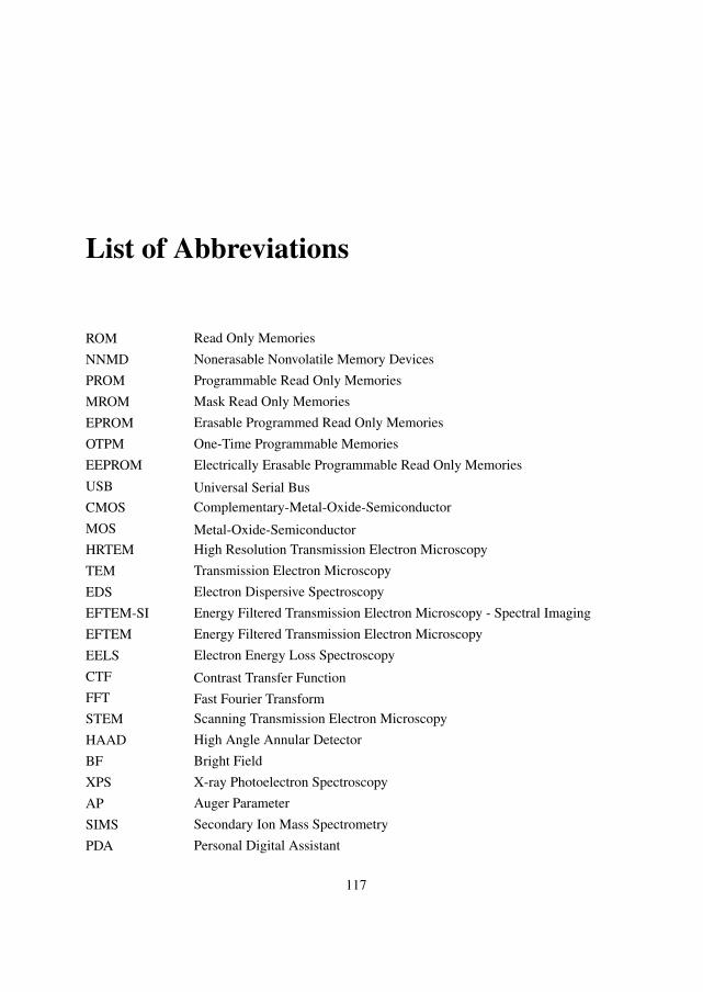
List of Abbreviations
ROM Read Only Memories
NNMD Nonerasable Nonvolatile Memory Devices
PROM Programmable Read Only Memories
MROM Mask Read Only Memories
EPROM Erasable Programmed Read Only Memories
OTPM One-Time Programmable Memories
EEPROM Electrically Erasable Programmable Read Only Memories
USB Universal Serial BusCMOS Complementary-Metal-Oxide-Semiconductor
MOS Metal-Oxide-SemiconductorHRTEM High Resolution Transmission Electron Microscopy
TEM Transmission Electron Microscopy
EDS Electron Dispersive Spectroscopy
EFTEM-SI Energy Filtered Transmission Electron Microscopy - Spectral Imaging
EFTEM Energy Filtered Transmission Electron Microscopy
EELS Electron Energy Loss Spectroscopy
CTF Contrast Transfer FunctionFFT Fast Fourier TransformSTEM Scanning Transmission Electron Microscopy
HAAD High Angle Annular Detector
BF Bright Field
XPS X-ray Photoelectron Spectroscopy
AP Auger Parameter
SIMS Secondary Ion Mass Spectrometry
PDA Personal Digital Assistant
117

RTO Rapid Thermal Oxidation
FCC Face Centred CubicHCP Hexagonal Closed Packed
BCC Body Centred Cubic
RCA Radio Corporation of America
PGM Platinum Group Metals
GM Granular Metal


![SEM, EDS AND XPS ANALYSIS OF NANOSTRUCTURED COATING …€¦ · as well as to SEM, EDS and XPS equipment, is presented in references [18÷21]. Figure 1 . EDS results of NiTi alloy](https://img.pdfslide.us/doc/110x75/5f0c3fca7e708231d434779c/sem-eds-and-xps-analysis-of-nanostructured-coating-as-well-as-to-sem-eds-and-xps.jpg)