Embed Size (px)
Citation preview
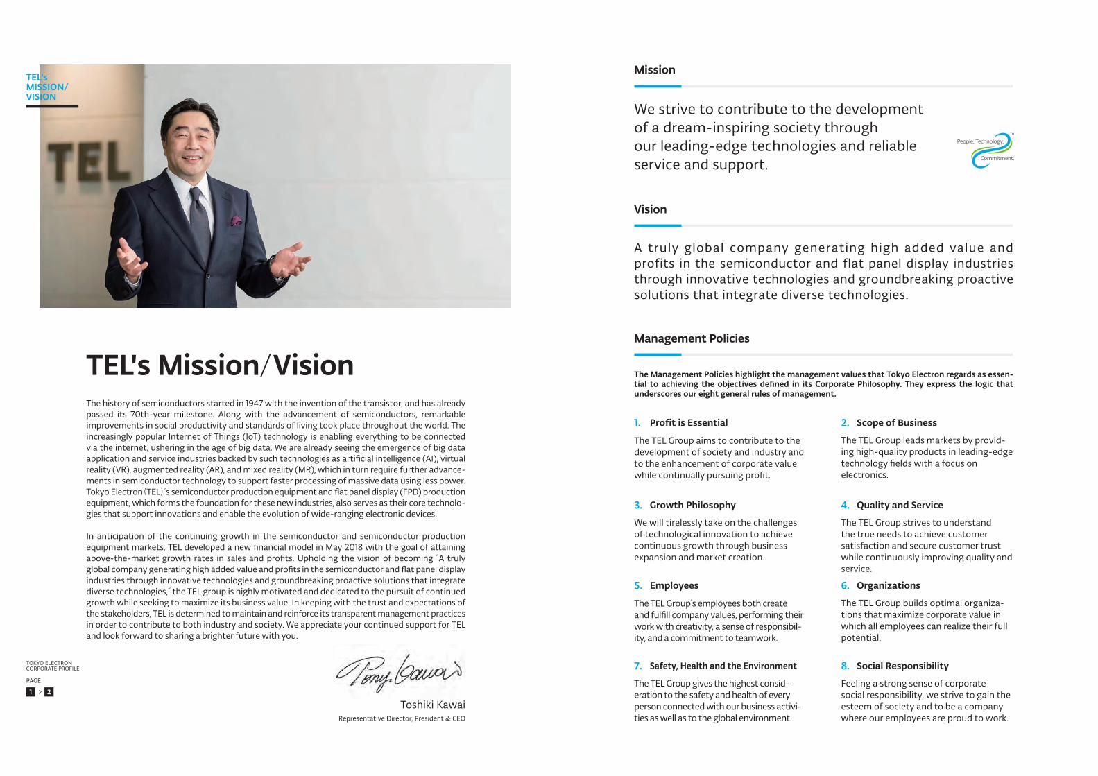
The TEL Group strives to understand the true needs to achieve customer satisfaction and secure customer trust while continuously improving quality and service.
4. Quality and Service
Feeling a strong sense of corporate social responsibility, we strive to gain the esteem of society and to be a company where our employees are proud to work.
8. Social Responsibility
The TEL Group gives the highest consid-eration to the safety and health of every person connected with our business activi-ties as well as to the global environment.
7. Safety, Health and the Environment
The TEL Group builds optimal organiza-tions that maximize corporate value in which all employees can realize their full potential.
6. Organizations
The TEL Group’s employees both create and fulfill company values, performing their work with creativity, a sense of responsibil-ity, and a commitment to teamwork.
5. Employees
The history of semiconductors started in 1947 with the invention of the transistor, and has already passed its 70th-year milestone. Along with the advancement of semiconductors, remarkable improvements in social productivity and standards of living took place throughout the world. The increasingly popular Internet of Things (IoT) technology is enabling everything to be connected via the internet, ushering in the age of big data. We are already seeing the emergence of big data application and service industries backed by such technologies as artificial intelligence (AI), virtual reality (VR), augmented reality (AR), and mixed reality (MR), which in turn require further advance-ments in semiconductor technology to support faster processing of massive data using less power. Tokyo Electron(TEL)’s semiconductor production equipment and flat panel display (FPD) production equipment, which forms the foundation for these new industries, also serves as their core technolo-gies that support innovations and enable the evolution of wide-ranging electronic devices.
In anticipation of the continuing growth in the semiconductor and semiconductor production equipment markets, TEL developed a new financial model in May 2018 with the goal of attaining above-the-market growth rates in sales and profits. Upholding the vision of becoming “A truly global company generating high added value and profits in the semiconductor and flat panel display industries through innovative technologies and groundbreaking proactive solutions that integrate diverse technologies,” the TEL group is highly motivated and dedicated to the pursuit of continued growth while seeking to maximize its business value. In keeping with the trust and expectations of the stakeholders, TEL is determined to maintain and reinforce its transparent management practices in order to contribute to both industry and society. We appreciate your continued support for TEL and look forward to sharing a brighter future with you.
2. Scope of Business
The TEL Group leads markets by provid-ing high-quality products in leading-edge technology fields with a focus on electronics.
TEL's Mission/Vision
Mission
Vision
Management Policies
A truly global company generating high added value and profits in the semiconductor and flat panel display industries through innovative technologies and groundbreaking proactive solutions that integrate diverse technologies.
We strive to contribute to the development of a dream-inspiring society through our leading-edge technologies and reliable service and support.
The Management Policies highlight the management values that Tokyo Electron regards as essen-tial to achieving the objectives defined in its Corporate Philosophy. They express the logic that underscores our eight general rules of management.
1. Profit is Essential
The TEL Group aims to contribute to the development of society and industry and to the enhancement of corporate value while continually pursuing profit.
3. Growth Philosophy
We will tirelessly take on the challenges of technological innovation to achieve continuous growth through business expansion and market creation.
Representative Director, President & CEO
Toshiki Kawai
TEL'sMISSION/VISION
TOKYO ELECTRONCORPORATE PROFILE
PAGE
21
12000
10000
8000
6000
4000
2000
0
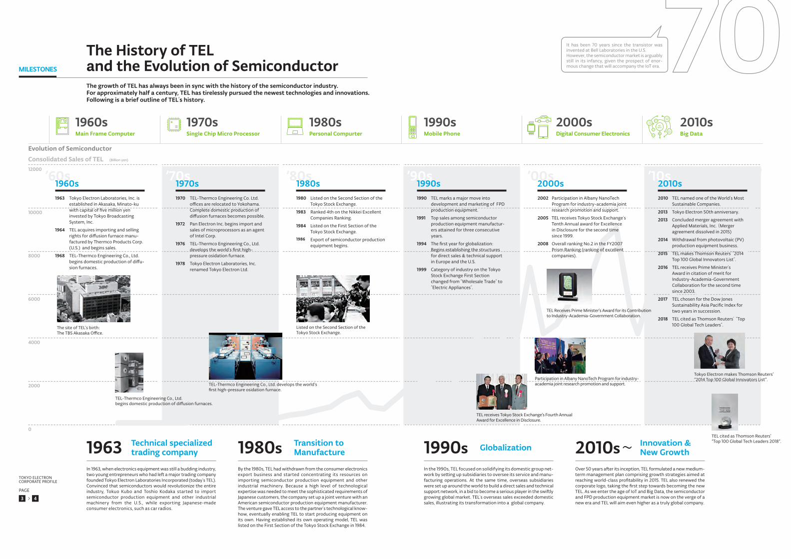
’70s’60s ’90s ’10s’80s ’00s(Billion yen)Consolidated Sales of TEL
The growth of TEL has always been in sync with the history of the semiconductor industry.For approximately half a century, TEL has tirelessly pursued the newest technologies and innovations. Following is a brief outline of TEL’s history.
It has been 70 years since the transistor was invented at Bell Laboratories in the U.S. However, the semiconductor market is arguably still in its infancy, given the prospect of enor-mous change that will accompany the IoT era.
TEL-Thermco Engineering Co. Ltd. offices are relocated to Yokohama. Complete domestic production of diffusion furnaces becomes possible.
Pan Electron Inc. begins import and sales of microprocessors as an agent of Intel Corp.
TEL-Thermco Engineering Co., Ltd. develops the world’s first high-pressure osidation furnace.
Tokyo Electron Laboratories, Inc. renamed Tokyo Electron Ltd.
1970
1972
1976
1978
1970sListed on the Second Section of the Tokyo Stock Exchange.
Ranked 4th on the Nikkei Excellent Companies Ranking.
Listed on the First Section of the Tokyo Stock Exchange.
Export of semiconductor production equipment begins.
1980
1983
1984
1986
1980sTEL marks a major move into development and marketing of FPD production equipment.
Top sales among semiconductor production equipment manufactur-ers attained for three consecutive years.
The first year for globalization: Begins establishing the structures for direct sales & technical support in Europe and the U.S.
Category of industry on the Tokyo Stock Exchange First Section changed from “Wholesale Trade” to “Electric Appliances”.
1990
1991
1994
1999
1990sParticipation in Albany NanoTech Program for industry-academia joint research promotion and support.
TEL receives Tokyo Stock Exchange’s Tenth Annual award for Excellence in Disclosure for the second time since 1999.
Overall ranking No.2 in the FY2007 Prism Ranking (ranking of excellent companies).
2002
2005
2008
2000sTEL named one of the World’s Most Sustainable Companies.
Tokyo Electron 50th anniversary.
Concluded merger agreement with Applied Materials, Inc. (Merger agreement dissolved in 2015)
Withdrawal from photovoltaic (PV) production equipment business.
TEL makes Thomson Reuters’ “2014 Top 100 Global Innovators List”.
TEL receives Prime Minister’s Award in citation of merit for Industry-Academia-Government Collaboration for the second time since 2003.
TEL chosen for the Dow Jones Sustainability Asia Pacific Index for two years in succession.
TEL cited as Thomson Reuters’ “Top 100 Global Tech Leaders”.
2010
2013
2013
2014
2015
2016
2017
2018
2010s
TEL-Thermco Engineering Co., Ltd. develops the world’s first high-pressure osidation furnace.
Listed on the Second Section of the Tokyo Stock Exchange.
TEL receives Tokyo Stock Exchange’s Fourth Annual Award for Excellence in Disclosure.
Participation in Albany NanoTech Program for industry-academia joint research promotion and support.
Tokyo Electron makes Thomson Reuters’ “2014 Top 100 Global Innovators List”.
TEL Receives Prime Minister’s Award for its Contribution to Industry-Academia-Government Collaboration.
TEL-Thermco Engineering Co., Ltd. begins domestic production of diffusion furnaces.
TEL cited as Thomson Reuters’“Top 100 Global Tech Leaders 2018”.1963 Technical specialized
trading company
In 1963, when electronics equipment was still a budding industry, two young entrepreneurs who had left a major trading company founded Tokyo Electron Laboratories Incorporated (today’s TEL). Convinced that semiconductors would revolutionize the entire industry, Tokuo Kubo and Toshio Kodaka started to import semiconductor production equipment and other industrial machinery from the U.S., while exporting Japanese-made consumer electronics, such as car radios.
1980s Transition to Manufacture
By the 1980s, TEL had withdrawn from the consumer electronics export business and started concentrating its resources on importing semiconductor production equipment and other industrial machinery. Because a high level of technological expertise was needed to meet the sophisticated requirements of Japanese customers, the company set up a joint venture with an American semiconductor production equipment manufacturer. The venture gave TEL access to the partner’s technological know-how, eventually enabling TEL to start producing equipment on its own. Having established its own operating model, TEL was listed on the First Section of the Tokyo Stock Exchange in 1984.
1990s Globalization
In the 1990s, TEL focused on solidifying its domestic group net-work by setting up subsidiaries to oversee its service and manu-facturing operations. At the same time, overseas subsidiaries were set up around the world to build a direct sales and technical support network, in a bid to become a serious player in the swiftly growing global market. TEL’s overseas sales exceeded domestic sales, illustrating its transformation into a global company.
Over 50 years after its inception, TEL formulated a new medium-term management plan comprising growth strategies aimed at reaching world-class profitability in 2015. TEL also renewed the corporate logo, taking the first step towards becoming the new TEL. As we enter the age of IoT and Big Data, the semiconductor and FPD production equipment market is now on the verge of a new era and TEL will aim even higher as a truly global company.
2010s Innovation & New Growth~
1960sTokyo Electron Laboratories, Inc. is established in Akasaka, Minato-ku with capital of five million yen invested by Tokyo Broadcasting System, Inc.
TEL acquires importing and selling rights for diffusion furnace manu-factured by Thermco Products Corp.(U.S.) and begins sales.
TEL-Thermco Engineering Co., Ltd. begins domestic production of diffu-sion furnaces.
1963
1964
1968
The History of TELand the Evolution of Semiconductor
The site of TEL’s birth: The TBS Akasaka Office.
Evolution of Semiconductor
1970sSingle Chip Micro Processor
1980sPersonal Compurter
1990sMobile Phone
2000sDigital Consumer Electronics
2010sBig Data
1960sMain Frame Computer
TOKYO ELECTRONCORPORATE PROFILE
PAGE
43
MILESTONES
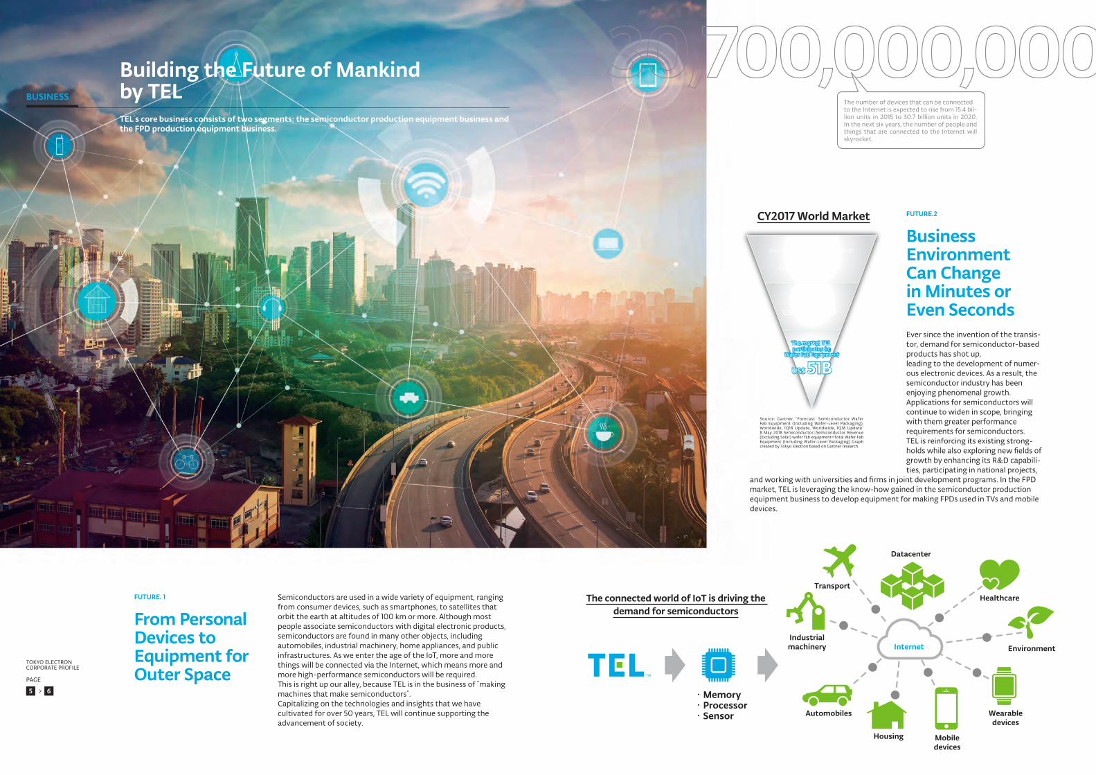
Building the Future of Mankind by TELTEL’s core business consists of two segments; the semiconductor production equipment business and the FPD production equipment business.
Semiconductors are used in a wide variety of equipment, ranging from consumer devices, such as smartphones, to satellites that orbit the earth at altitudes of 100 km or more. Although most people associate semiconductors with digital electronic products, semiconductors are found in many other objects, including automobiles, industrial machinery, home appliances, and public infrastructures. As we enter the age of the IoT, more and more things will be connected via the Internet, which means more and more high-performance semiconductors will be required. This is right up our alley, because TEL is in the business of “making machines that make semiconductors”.Capitalizing on the technologies and insights that we have cultivated for over 50 years, TEL will continue supporting the advancement of society.
Ever since the invention of the transis-tor, demand for semiconductor-based products has shot up,leading to the development of numer-ous electronic devices. As a result, the semiconductor industry has been enjoying phenomenal growth. Applications for semiconductors will continue to widen in scope, bringing with them greater performance requirements for semiconductors. TEL is reinforcing its existing strong-holds while also exploring new fields of growth by enhancing its R&D capabili-ties, participating in national projects,
and working with universities and firms in joint development programs. In the FPD market, TEL is leveraging the know-how gained in the semiconductor production equipment business to develop equipment for making FPDs used in TVs and mobile devices.
FUTURE.2
Business Environment Can Change in Minutes or Even Seconds
CY2017 World Market
Source: Gartner, “Forecast: Semiconductor Wafer Fab Equipment (Including Wafer-Level Packaging), Worldwide, 1Q18 Update, Worldwide, 1Q18 Update”8 May 2018 Semiconductor=Semiconductor Revenue (Excluding Solar) wafer fab equipment=Total Wafer Fab Equipment (Including Wafer-Level Packaging) Graph created by Tokyo Electron based on Gartner research.
The connected world of IoT is driving the demand for semiconductors
The number of devices that can be connected to the Internet is expected to rise from 15.4 bil-lion units in 2015 to 30.7 billion units in 2020. In the next six years, the number of people and things that are connected to the Internet will skyrocket.
FUTURE. 1
From Personal Devices to Equipment forOuter Space
Environment
Wearable devices
Mobile devices
Housing
Automobiles
Industrial machinery
Transport
Datacenter
Internet
Healthcare
・Memory・Processor・Sensor
BUSINESS
TOKYO ELECTRONCORPORATE PROFILE
PAGE
65
Leading-edge Manufacturing Expertise and Outstanding ServicesTEL mainly operates two lines of business: semiconductor production equipment and flatpanel display (FPD) production equipment. TEL develops diverse semiconductor production equipment that covers principal chip manufacturing processes, supplying these systems, along with excellent technical support, to semiconductor manufacturers worldwide. Many of the products that are devel-oped, manufactured, and sold by TEL hold leading positions in the global market.
Semiconductors are key components of a wide variety of digital products, including laptops, smartphones, digital cameras, automobiles, and household appliances. TEL develops diverse semi- conductor production equipment that covers principal chip manufacturing pro- cesses, and supplies these systems to semiconductor manufacturers world-wide along with excellent technical support.
Semiconductor Production Equipment
What is the Nano-level World?
COLUMN
The surface of semiconductors is intricately structured, with feature dimensions typically in the order of tens to hundreds of nanometers. This is a scale comparable to that of viruses and the diameter of the DNA double helix. As nanotechnology-enabled semiconductor production equipment shrank the feature size of semiconductors, it became possible to make mobile devices such as laptops and smartphones thinner, faster, and lighter.
More about Nanoscale at: www.tel.com/museum/
Lymphocyte
Virus
DNA
Integrated circuit pattern
10μm
800nm
22 nm
2 nm
1 nm is one-billionth of a meter. 1 μm is one-thousandth of a millimeter, and 1 nm is one-thousandth of that. Semiconductor manufacturing today involves nanoscale operations at the atomic and molecular level.μm: micrometer, nm: nanometer
Thermal ProcessingSystem
TELINDY PLUS™
Plasma Etch System
Tactras™
Coater/Developer
CLEAN TRACK™
LITHIUS Pro™ Z
Single Wafer Cleaning System
CELLESTA ™-i
Single Wafer Depostion System
Triase+™
Atomic Layer Deposition System
NT333™
Wafer Prober
Precio™/Precio™ XL
ElectrochemicalDeposition System
Stratus™
Wafer Bonder/Debonder
Synapse™ V/Synapse™ Z Plus
Wafer/Dicing Frame Prober
WDF™ 12DP+
Plasma Etch System
Tactras™
Single Wafer Deposition System
Triase+™
Contact formationIsolation formation, Gate formationPa�ern formation
DRAM, Logic, 3D NAND, etc.
Semiconductor Manufacturing Process
Another dielectric layer is deposited on top, in which trenches are etched to form yet another wiring pa�ern. The trenches are filled with a metal film, and then the excess metals are polished and the surface is planarized. These processes are repeated to make a multi level interconnect.
Each integrated circuit is tested by a wafer prober to find any failed circuits.
In this process, the wafer is covered with a UBM* layer and then pa�erned, on which metal layers are deposited to form redistribution layers and bump electrodes.
*UBM:Under Bamp Metal
The back grinding equipment is used to reduce the wafer thickness. A support substrate or support wafer may be temporarily bonded to the wafer to facilitate grinding, and is then removed by a debonder.
The wafer is diced into separate chips by a cu�er, and only the good chips make it into the final assembly.
The chips are a�ached to package substrates or lead frames, and are sealed with ceramic or plastic.
To transfer the integrated circuit pa�ern*1 onto a wafer, an equipment called stepper irradiates UV light on the photoresist layer through a pa�erned photomask*2 aligned over the wafer.
Developing exposed photoresist leaves a particular pa�ern on a wafer according to the reticle (photomask) being used.
A plasma etch system removes the exposed dielectric silicon dioxide/nitride layer from the wafer surface according to the remaining photoresist.
In a post-etch process, the residual photoresist is removed, and the wafer is soaked into chemical solvents to remove particles and impurities on the wafer.
A layer of dielectric material (silicon dioxide) is deposited into the pa�erned trenches to isolate individual transistors (elements).
Gates are formed a�er gate dielectric and electrode layers are stacked by oxidation, CVD*, and/or ALD**. A�er that, silicon nitride layers are deposited by CVD* and/or ALD**.
*CVD:Chemical Vapor Deposition**ALD:Atomic Layer Deposition
To form wiring that connects individual transistors, first a dielectric (oxide) layer is deposited over the gate layer so another layer of circuit can be laid on top. Contact holes (vias) are then opened in the dielectric layer, and are filled with metal by CVD.
Interconnect formation Wafer probe testing Bump formation Wafer bonding/thinning/debonding
Inspection/dicing process
Assembly process
Pa�ern design *1
Photomask fabrication *2
The front-end process for FPD production (known as the TFT array process) is similar to the semiconductor manufacturing process.
Various circuit modules are combined to create circuit pa�erns that satisfy functional requirements.
Reticles (photomasks) are fabricated which enable device components to be laid out by exposure as designed .
Wafer
Silicon dioxide film
Silicon nitride film Photoresist Dielectric film Metal film
Metal film
Intermetal dielectric film
Wafer process (Front-end) Assembly and Test process (Back-end)
Oxide/nitride film deposition
As a pre-processing procedure, the surface of a wafer is thoroughly cleaned. This is followed by thermal processing, in which a thin film of silicon dioxide or silicon nitride is formed on the wafer surface.
Photoresist* coatingWhile the wafer is rotated at a high speed, a thin layer of photoresist is coated uniformly on its surface.
* Photoresist: a light-sensitive material that changes its properties when exposed to ultraviolet (UV) light.
Exposure Development Etching Ashing/Cleaning
Logic
DRAM
3D NAND
PRODUCT
TOKYO ELECTRONCORPORATE PROFILE
PAGE
87
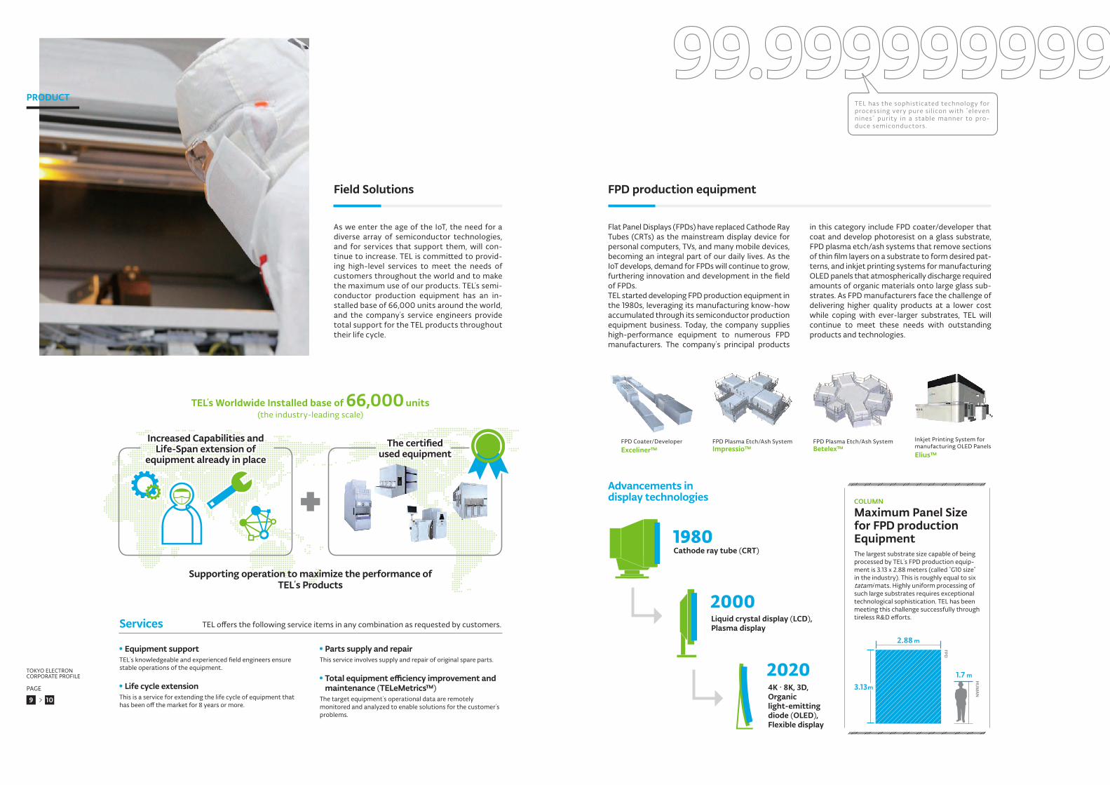
As we enter the age of the IoT, the need for a diverse array of semiconductor technologies, and for services that support them, will con-tinue to increase. TEL is committed to provid-ing high-level services to meet the needs of customers throughout the world and to make the maximum use of our products. TEL’s semi-conductor production equipment has an in- stalled base of 66,000 units around the world, and the company’s service engineers provide total support for the TEL products throughout their life cycle.
Flat Panel Displays (FPDs) have replaced Cathode Ray Tubes (CRTs) as the mainstream display device for personal computers, TVs, and many mobile devices, becoming an integral part of our daily lives. As the IoT develops, demand for FPDs will continue to grow, furthering innovation and development in the field of FPDs. TEL started developing FPD production equipment in the 1980s, leveraging its manufacturing know-how accumulated through its semiconductor production equipment business. Today, the company supplies high-performance equipment to numerous FPD manufacturers. The company’s principal products
in this category include FPD coater/developer that coat and develop photoresist on a glass substrate, FPD plasma etch/ash systems that remove sections of thin film layers on a substrate to form desired pat-terns, and inkjet printing systems for manufacturing OLED panels that atmospherically discharge required amounts of organic materials onto large glass sub-strates. As FPD manufacturers face the challenge of delivering higher quality products at a lower cost while coping with ever-larger substrates, TEL will continue to meet these needs with outstanding products and technologies.
Supporting operation to maximize the performance ofTEL’s Products
TEL has the sophisticated technology for processing very pure silicon with “eleven nines” purity in a stable manner to pro-duce semiconductors.
Increased Capabilities andLife-Span extension of
equipment already in place
Increased Capabilities andLife-Span extension of
equipment already in place
The certified used equipment
The certified used equipment
Field Solutions FPD production equipment
Impressio™FPD Plasma Etch/Ash System
Betelex™FPD Plasma Etch/Ash System
Elius™
Inkjet Printing System for manufacturing OLED PanelsExceliner™
FPD Coater/Developer
1.7 m
2.88 m
3.13m
HU
MA
N
FPD
Maximum Panel Size for FPD production Equipment
COLUMN
The largest substrate size capable of being processed by TEL’s FPD production equip-ment is 3.13 x 2.88 meters (called “G10 size” in the industry). This is roughly equal to six tatami mats. Highly uniform processing of such large substrates requires exceptional technological sophistication. TEL has been meeting this challenge successfully through tireless R&D efforts.
This service involves supply and repair of original spare parts.
Parts supply and repair
TEL offers the following service items in any combination as requested by customers.Services
TEL’s knowledgeable and experienced field engineers ensure stable operations of the equipment.
Equipment support
This is a service for extending the life cycle of equipment that has been off the market for 8 years or more.
Life cycle extensionThe target equipment’s operational data are remotely monitored and analyzed to enable solutions for the customer’s problems.
Total equipment efficiency improvement and maintenance (TELeMetrics™)
TEL’s Worldwide Installed base of 66,000 units(the industry-leading scale)
1980
2000
2020
ブラウン管
液晶
プラズマ
4K・8K3D(3次元)有機 ELフレキシブル
Advancements in display technologies
4K・8K, 3D, Organic light-emitting diode (OLED), Flexible display
Liquid crystal display (LCD), Plasma display
Cathode ray tube (CRT)
PRODUCT
TOKYO ELECTRONCORPORATE PROFILE
PAGE
109
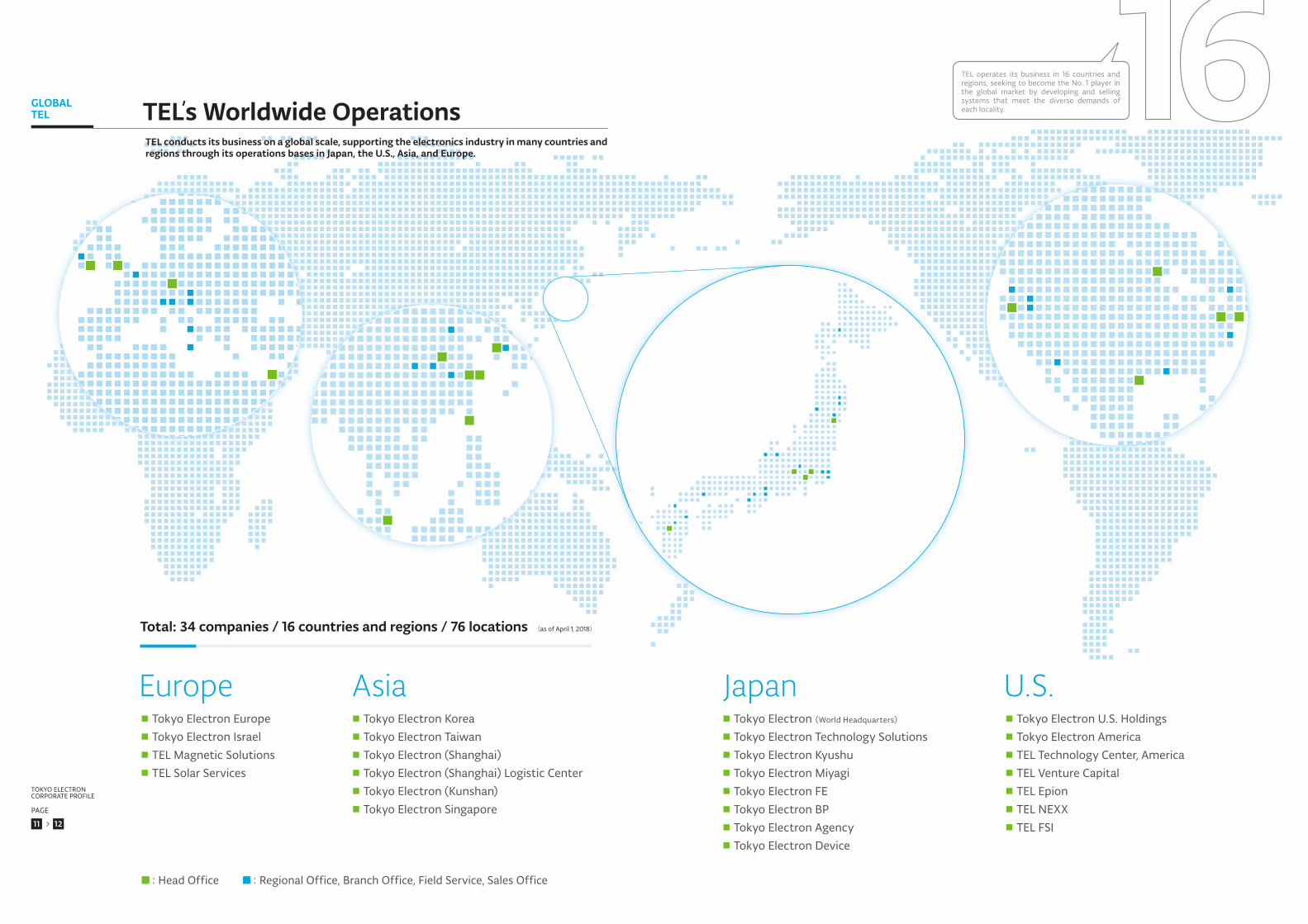
TEL conducts its business on a global scale, supporting the electronics industry in many countries and regions through its operations bases in Japan, the U.S., Asia, and Europe.
TEL’s Worldwide Operations
TEL operates its business in 16 countries and regions, seeking to become the No. 1 player in the global market by developing and selling systems that meet the diverse demands of each locality.
Total: 34 companies / 16 countries and regions / 76 locations (as of April 1, 2018)
GLOBAL TEL
TOKYO ELECTRONCORPORATE PROFILE
PAGE
1211
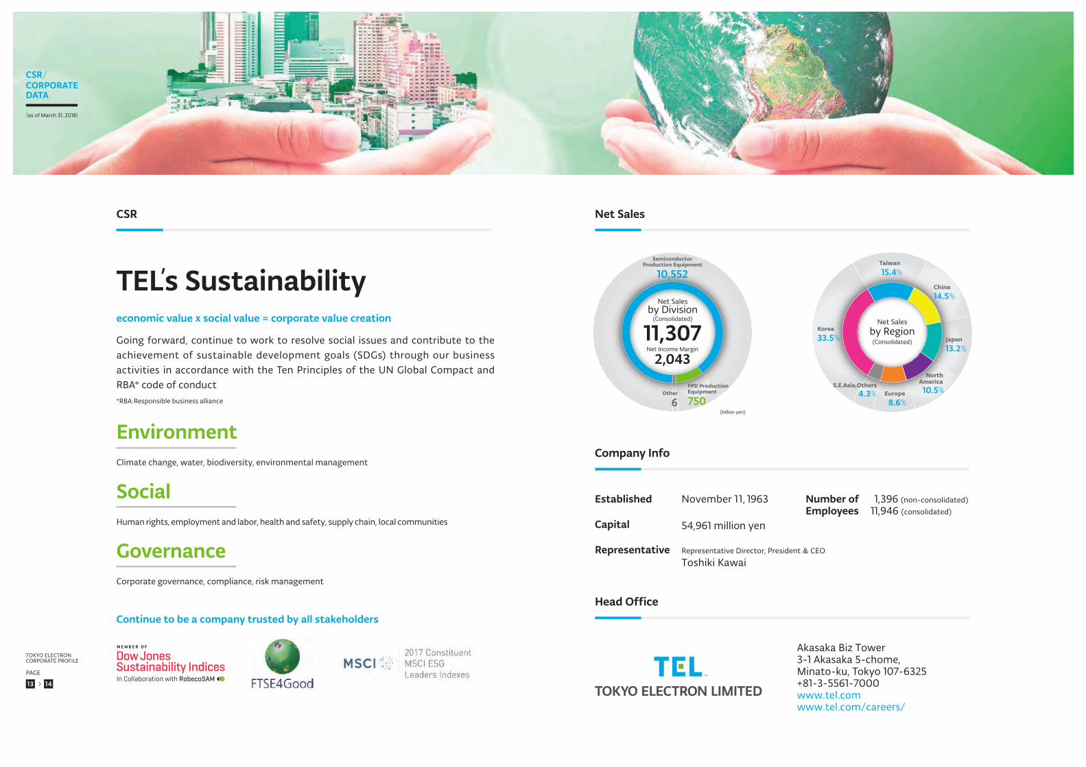
Established November 11, 1963
54,961 million yenCapital
1,396 (non-consolidated)
11,946 (consolidated)
Number of Employees
Representative Director, President & CEO
Toshiki KawaiRepresentative
Company Info
Net Income Margin
11,3072,043
Net Salesby Division
(Consolidated)
(billion yen)
SemiconductorProduction Equipment
10,552
FPD Production Equipment
750Other
6
Net Salesby Region(Consolidated)
Korea
33.5%
China
14.5%
Japan
13.2%
North America10.5%Europe
8.6%
S.E.Asia,Others4.3%
Taiwan
15.4%
Net Sales
Going forward, continue to work to resolve social issues and contribute to the achievement of sustainable development goals (SDGs) through our business activities in accordance with the Ten Principles of the UN Global Compact and RBA* code of conduct
Continue to be a company trusted by all stakeholders
CSR
economic value x social value = corporate value creation
TEL’s Sustainability
Climate change, water, biodiversity, environmental management
Environment
Human rights, employment and labor, health and safety, supply chain, local communities
Social
Corporate governance, compliance, risk management
Governance
Head Office
Akasaka Biz Tower3-1 Akasaka 5-chome,Minato-ku, Tokyo 107-6325+81-3-5561-7000www.tel.comwww.tel.com/careers/
*RBA:Responsible business alliance
TOKYO ELECTRONCORPORATE PROFILE
PAGE
1413
CORPORATEDATA
CSR/
(as of March 31, 2018)

Akasaka Biz Tower, 3-1 Akasaka 5-chomeMinato-ku, Tokyo 107-6325, JapanTel.+81-3-5561-7000www.tel.com
TEL is a registered trademark or a trademark of Tokyo Electron Limited in Japan and/or other countries.PR56-146