Embed Size (px)
Citation preview
265 OSBORNE ROAD 0 ALBANY, N. Y. 12211
Tel 459-7350 (Area Cod. S17)
C.W. X-BAND VOLTAGE TUNABLE OSCILLATOR
Report Number 9
Contract Number DA-36-039 AMC-03270 (E)
CY Department of the Army Task No. lP6-22001-A-055-04
Final Report
1 July 1963 to 31 October 1965
U. S. ARMY ELECTRONICS COMMAND
FORT MONMOUTH, NEW JERSECLEA R N GH% '
FOR FEDF' AT , ...EC:Tp r C.•• , r , -
Mictron Inc.
265 Osborne Road Rl_
Albany, New York 12211 •6t& (
C.W.' X-BAND VOLTAGE TUNABLE OSCILLATOR
Report Number 9
Contract Number DA-36-039 AMC-03270(E)
Electronics Command Technical Requirement Number SCL-7001/86
dated 21 November 1962
Department of the Army Task No. IP6-22001-A-055-04
Final Report
1 July 1963 to 31 October 1965
Object: To conduct an investigation of a C.W. X-Band
Voltage Tunable Oscillator in accordance with
Electronics Command Technical Requirement
Number SCL-7001/86 and deliver six experimental
models that are representative of work
accomplished during the investigation.
Report prepared by
Dr. M. R. Boyd
~T F
TABLE OF CONTENTS
Page
SPURPOSE.. .. . . . . . .. . . . . . I
-!ABSTRACT.. . . ... o ................ 00 00 00 2
PUBLICATIONS,, LECTURES,, REPORTS AND CONFERENCES . . .o. . .. .. 3
Conferences .. . .. .. .. .. . . . . . . .. . . . . . . . 3
FACTUAL DATA* . e o .* o e a o * .... 4
I I Introduction o o 0 * 0 0 * . . . . . a . . . 4
II Design II Program . 0 . ........ . ......... 7
I Illustrations:
I Figure 1 Design II Cross Section ......o.. o. o 7
Figure 2 Design II Showing Components Parts *... ... 8
I Figure 3 Design II In Waveguide Mounting I * 0 0 0 * 10
Figure 4 Photo Showing Performance Data (Design II)... 11
I Figure 5 Photo Showing Performance Data (Design II). . 11
Figure 6 Section Showing Strap Modification ...... 12
Figure 7 Photo Showing Performance Data (High Frequency) 12
j Figure 8 Photo Illustrating Control Range Stability . • 13
III Design I Program. * * ........ ... ....... 16
Figure 10 Distribution of Fields on Vanes . . . *16
Figure 11 Design I Cross Section . ....... . . 17
IV Modified Design I (Short Tube) . .. .. .. . . .. ... 20
I Figure 12 Cathode Modification Experiment . . . . ... 20
Figure 13 Diagram of Tab-Vane Tube . . . . . . . 21
I Figure 14 Illustration of Vane Tip Theory ....... 22
Figure 15 Cross Section Modified Design I . . . . 24
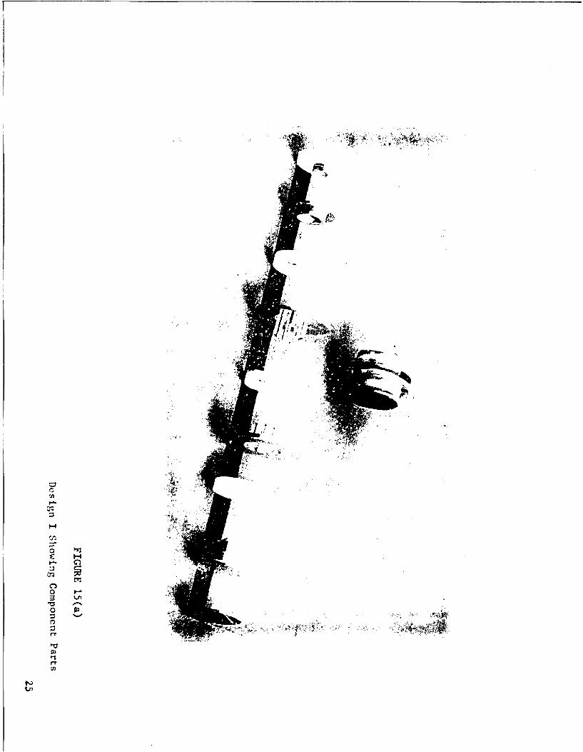
Figure 15a Design I Showing Component Parts ...... 25
IC
Dag
Continued P
Figure 16 Photo Showing Performance lata(Modified Design I) . . . .0. . .0 . . . . . . . . 27
Figure 17 Circuit Assembly . . .0. . . . . . . *.. .. .29
Figure 18 Photo Showing Circuit Tube Assembly . .&. . . . . 30
Figure 19 Photo Showing Circuit in Test Set-Up . . . . . . 31
Figure 20 Photo Showing Packaged Unit with Isolator-Adapter 32
Figure 21 Photo Showing Packaged Unit with TNC Output . . . 33
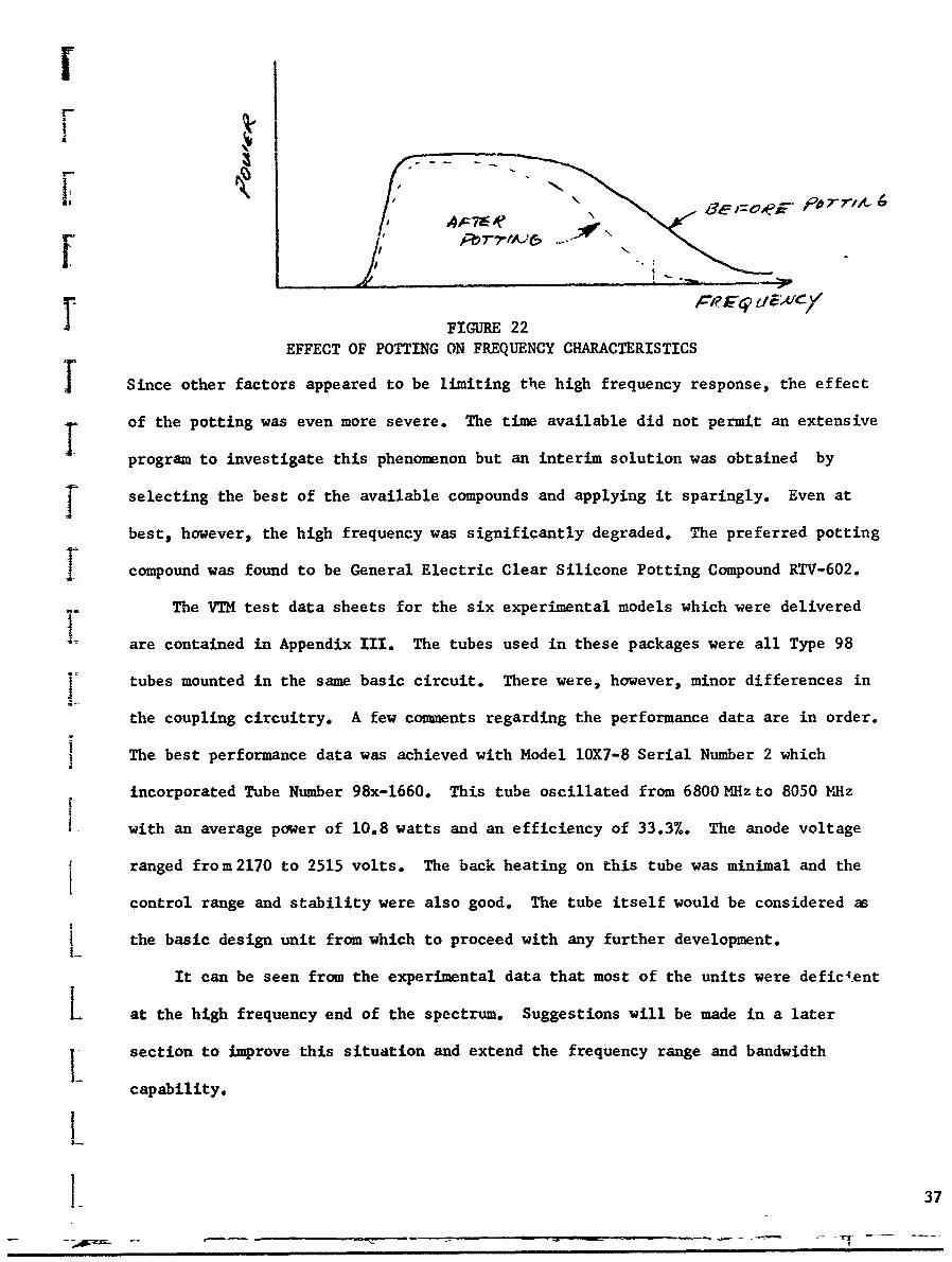
Figure 22 Illustration of Effect of Potting . . .0. . . . . 37
Figure 23 Photo Showing Noise Performance Data ...... 39
OVERALL SUMMARY AND RECOMMENDATIONS . . . . . . . . . . . .... 41
APPENDIX I . . . . . . . . . . ......... 4 * * * 4
Specification... .................... 44
APPENDIX II . . . ....................... 50
Technology of Tube Fabrication .. . . . .. .. . . .. . 50
APPENDIX I11 * o * * * o * o * . ........ . .51
Chart I (Design II Tube Data) .... . . . .. .. .* 51
Chart II (Design I Tube Data) .o. . . . .0. .. .... * . . 53
Chart III (Modified Design I Short Tube Data) . . . . . . . 54
Chart IV Miscellaneous Tube Data ...... . ...... 56
APPENDIX IV.... .... .. .. .. . . . . . . . . 58
Tube Performance Data Sheets. . o . ..... . . 58
I
PUiRPOSEIThe purp-se of this contract is to conduct an investigation
of a C.W. X-Band Voltage Tunable Oscillator in accordance with Electronics
Command Technical Requirement Number SCL-7001/86 and to deliver six
I experimental models that are representative of work accomplished during
the investigation.
This research and development program wil.. be conducted in
t"7o phases.
Phase I Research Phase
SPhase II Development Phase - Delivery of six developmentsamples
I:UV
I:[U
ABSTRACT
The design objectives for a 10 watt X-Band VTM are discussed and the
prior art is reviewed. The general approach is evolved from considerations of
the problem of mode stability and coupling. Two basic designs are presented, one
interdigital and one consisting of a novel approach with the cavities integral
to the vacuum device.
Detailed information on the theory of each of the basic designs is
given as well as information on the fabrication of the units. Circuit configurations
are discussed and a suitable circuit for each of the designs is evolved. A
chronological review of all results of operating tubes is given with discussions
of important design changes and the reasons for them.
Units were developed which exceeded the objective specifications, the
most significant performance being 14 watts at 33% efficiency over the 7.0 to 8.0 GHz
band. The principal problem area, a lack of consistency in results obtained, is
discussed in detail. The composite results are analyzed in terms of the objectives
and recommendations are made for further development.
i2
FACTUAL DATA3'
S~I INTRODUCTION
The principal objective of the subject program was to conduct a research and
development effort leading to a Voltage Tunable Magnetron for tl~e low X-Band fre-
N I' quency range. The objective specifications are contained in Signal Corps Technical
Requirements SCL-7001/86 dated 21 November 1962. For reference, this document has
been included as Appendix I of this report.
Although the mechanism of voltage tuning of magnetrons had been demonstrated
some fifteen years prior to this contract, most of the subsequent effort was devoted
I to development in the lower frequency ranges. (For a more comprehensive discussion
of prior developments, the reader is referred to Quarterly Progress Report Number 1
issued during the subject program.) The feasibility of operation at X-Band had been
demonstrated, but little information of a design nature could be derived from previous
programs. The performance of lower frequency VTM's must still provide the basis for
* X-Band designs.
The general philosophy of the approach which was undertaken merits some discussion
" insofar as it affected the nature of the subsequent program. The approach was to be
primarily experimental and based upon the study of operating units. There would be
h both theoretical analysis and cold-test experimental work, but major emphasis would be
Sanalysis of experimental tubes. There were several reasons for pursuing this type of
effort. As an oscillator, the VTM isa non-linear device with a nebulous theory of
L operation and, as such, is not amenable to meaningful analysis. Since the objectives
were primarily experimental, so was the approach. Unlike many other microwave tubes,
the basic VTM unit is relatively inexpensive and can be fabricated quickly. This
L characteristic of the device was responsible for the concentration of effort on
operating devices rather than on cold test experiments. Of course, a further con-
f L sideration is that the end product itself must be an operating device.
9 L
C)0
ZZ
n'em10
O'~~j1C( t~Ui 'l
CD(D
> > pro. a,
'10a0*& -AtýO W1~0 D a1.0 D la.( wO C t' CN tA'0 I O 1"
cr ul ( cr Lno 0 cr " (oc o. Lqn0 o~ 0 Co Ln 0
Pt Ft ft P w0 t )t
0 0 0-3 00
t4 -4K t4i! 4 K-40D~ 0.0 t 0 C
0: 0
1-d~~~- La) tvZ: 4 1d V 0: -4 P -
SW CLn r.0 000w0 0 b0M :E 0 0' 0'
rt Ut UttA
00
09) ýo ( uoDUC QD ~ i
rt pt >t0 F t 0 C ' t F
0 0 po 0
m t* a 0 0 Fs.4 % rt m 4At
Irt'
OQ 500)
m 0% 0% * . . * . * *
0 tJ 5.'f rt5 ft 03' Ft Ftmt pt~ 0t ?1 : F0p i 01t 14 Ft "F
r
After considering previous experience in both low frequency and X.Band areas,
[ the decision was made to pursue a program which would evaluate three approaches
simultaneously. These were:
1.) Interdigital structure operated in pi-mode (Design I)
2.) Vane-type anode circuit operated in pi-mode (Design II)
3.) "e-mode" operation
Design I and Design II programs were activated at the outset and conducted simulta-
I neously. A few special tubes were designed to enhance e-mode operation but this
program consisted mainly of evaluating e-mode oscillations in the Designs I and II
types. These results will be discussed further in a later section.
The design of the interaction space is comnon to both Designs I and II and is
based on conventional magnetron design equations:
fi (1) Va - 3040 BQa 2 -dc 2 )
"N A(2) Vc - 0.0356B2 (da2-dc2 ) 2
daZ
(3) 1-k=1 Va7 VC
I where Va anode to cathode voltage in volts
B magnetic field in gauss
I da- anode diameter in inches
[ dc -cathode diameter in inches
N - number of vanes
[ A - wavelength in cm. of 7-mode freq.
Vc - Hull cutoff voltagea:~ " theoretical efficiency
L 1 See, for example, Vacuum Tubes by Spangenberg. McGraw-Hill 1948 Chapter 18.
rr
The parameters specified initially are:
Va m 2250 volts (center voltage)
N 18 vanes
- 4 cm (fn - 7500 Mc)
da * 0.160 inches
dc - 0.110 inches
The remaining parameters may be computed using Equations (1), (2) and (3)
These are:
B - 3950 gauss
Vc= 3950 volts
7 - 43% (theoretical)
Based on previous experience, the interaction length was chosen as:
I = 0.170 inches
The choice of the interaction length of 0.170 inches merits some comment. Some
limited experimental evidence at lower frequencies had indicated that performance
would degrade if the interaction length was reduced below a "critical" value. To
avoid this possibility the aspect ratio, i.e., the ratio of anode diameter to interaction
length, was made to be consistent with lower frequency designs of proven capability.
The interaction length later proved to be a critical parameter as will be seen.
6
-A-0-
N~
cji
rt
OD
II DESIGN II PROGRAM
A discussion of the modes in multicavity magnetron structures is given in
Quarterly Report #1, Page 7-14. This material is included as Appendix V of this report.
The concept of Design II evolved from these considerations of modes as well as the
problems of heavily loading cavity magnetrons. A cross section of the Design II model
is shown in Figure 1.
OtrS~tra2pVanes
OInner_ Str-ap... S
N XI
FIGURE 1
DESIGN II CROSS SECTION
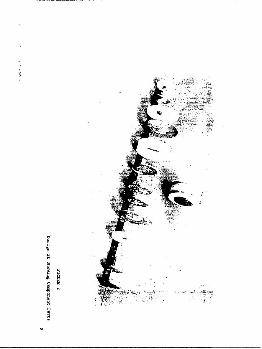
A photograph of the assembled unit is shown in Figure 2 with the component parts. The
strapping and coupling are the unique features of this particular design. The heavy
disc strapping was utilized to separate modes and also provide a symmetrical means by
which to couple power out.
In Appendix II the technology of tube fabrication is outlined as it applies to
both Design I and Design II. The particular feature of Design II which merits comment
in this secticn is the anode sub-assembly. The anode block itself is made by Electro-
Discharge-Machining a blank slug which has been machined to dimension. The unit is
then chemically processed and fired prior to assembly. The inner (small diameter)
straps are brazed to alternate sets of vanes on the anode block. This unit is then
sub-assembled with the outer (large diameter) straps and the ceramic window. Brazing
material is required between each vane and each tab to the disc straps - a total of 36
braze points in addition to the ceramic seals of the sub-assembly.
7
I
The anode window sub-assembly is then combined with a filament assembly and a control
c!ectrode and brazed (with an alignment jig) into a body which is complete except for
the cold cathode. The cold cathode is brazed at a lower temperature into the str'.cture
after the alignment jig has been removed.
The vane-to-vane spacing of the anode blocks could be held to close (0.001")
tolerance by the EDM process, but a technology problem which caused radial staggering
of the vanes arose during the fabrication of Design II tubes. This was due to the
fact that alternate vanes were brazed to the outer strap which was then sealed to the
ceramic window in a subsequent braze. Since this braze occurs at approximately 1000oC.5
the copper parts have expanded more than the ceramic window. Upon cooling, the
ceramic-to-metal braze then held these alternate vanes at a greater radius causing
staggering. An attempt to improve this; situation was made by preofabricating the
anode sub-structure with niobium (columbium) inner straps. The idea here was to
cause the set of vanes not tied to the outer strap to be set radially outward by a
similar process. This improved the situation but the problem remained in a lesser
degree. The exact effect of this radial staggering 'jould not be fully determined
because units without some degree of staggering could not be built. The best results
were obtained with units where the vanes were formed around a mandrel after the sub-
assemblies had been brazed.
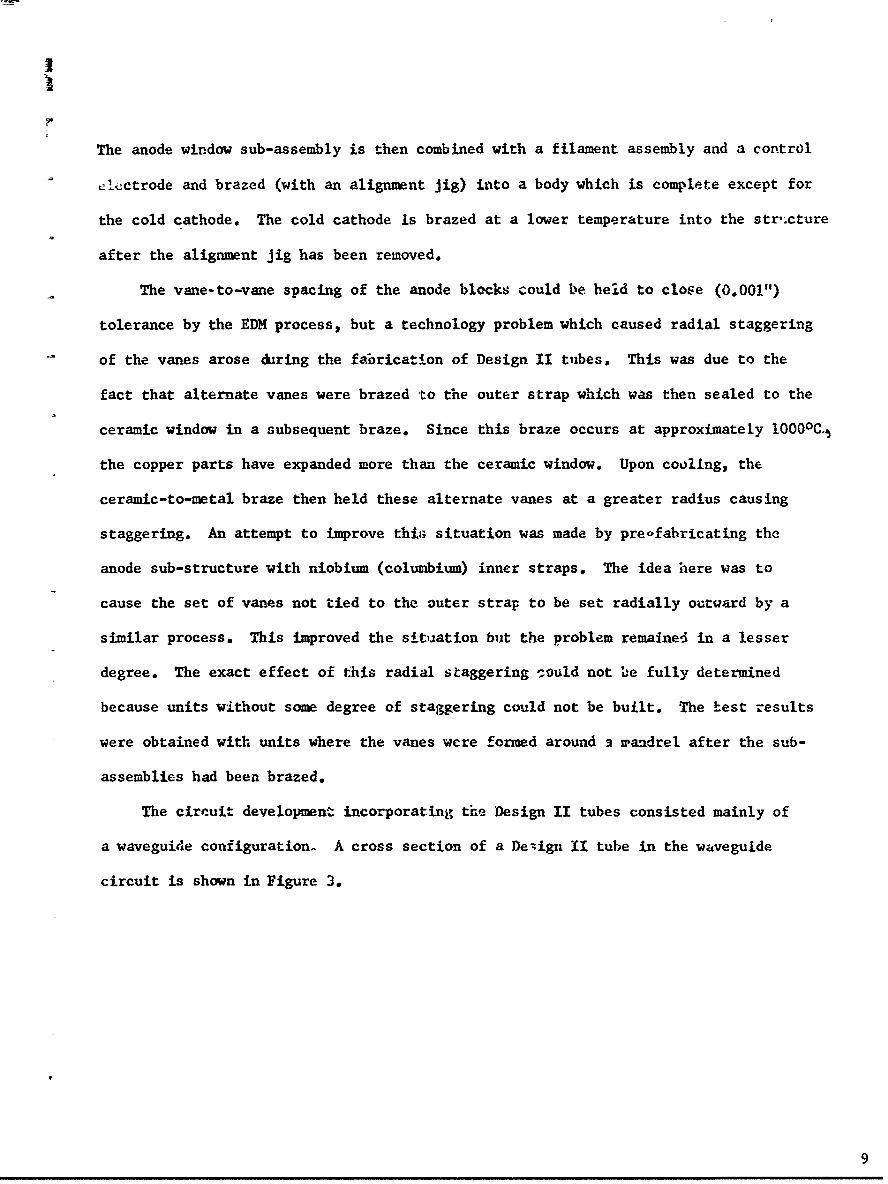
The circuit development incorporating the Design II tubes consisted mainly of
a waveguide configuration- A cross section of a Deiign 1I tube in the wavegulde
circuit is shown in Figure 3.
9
FLANGE
IND.VCTLTE SHORTING PLANERG 50U WAVEGUIDE
S"-,.DESIGNq II !TUBE
FIGURE 3CROSS SECTION DESIGN II MOUNTED IN WAVEGUIDE CIRCUIT
A sliding sbort having finger contacts provided the inductive circuit by which the
tube capacity was tuned to the frequency of interest, in general, operation in the
7.0 to 8.0 Gc band was obtained by pushing the short in close proximity to the window
ceramic. Similar operation could be obtained by the short being placed a half wave-
length (approximately 2 cm.) from the window, but there was a tendency for the VTM to
operate at a lower frequency more effectively than the oscillation at X-Band.
Several circuit configurations were tried in an attempt to match the device over
the band of interest. These consisted of inductive and/or capacitative irises inserted
between the tube and the waveguide output. All of these matching circuits, however,
had the effect of restricting the band of oscillation. Progress in this area was
limited because of two reasons. The behavior of the tubes in the circuitry indicated
that the thickness of the window ceramic and its diameter prevented access of the
coupling network to the fields.
910
* In other words. it appeared that in order to be effective, the coupling network should
[ be incorporated in the vacuum device. Because of the empirical design of these com-
ponents and the difficulty of fabricating vacuum devices this approach was not
E seriously pursued. Another difficulty in the development of wideband waveguide
circuitry was the limited number of waveguide configurations which could be tried and
I the inaccessibility of the waveguide fields, during testing. The tube alignment in
T the magnet would have to be disturbed for each position of an iris that was being in-
yes tigated.
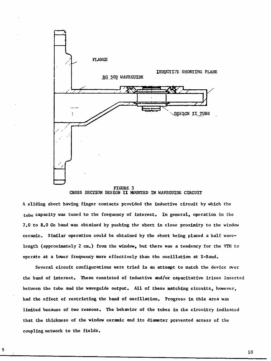
T In spite of inherent problems of tube fabrication and circuit development,
sufficient data were obtained to encourage the continuation of the Design II approach.
I Some of the more significant results are shown in Figures 4, 5.
r
FIGURE 4 FIGURE 5FREQUENCY-POWER RESPONSE DESIGN II FREQUENCY-POWER RESPONSE DESIGN II
UNIT UNIT
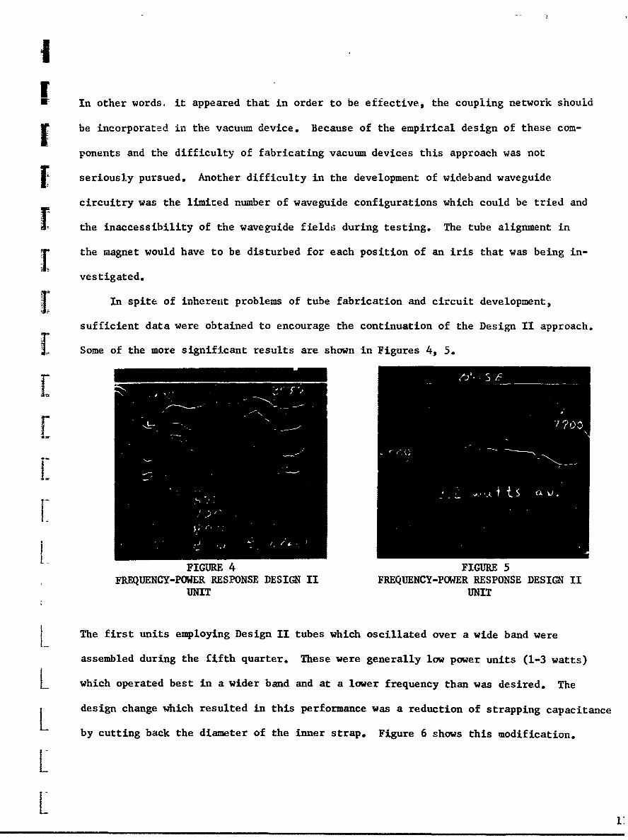
The first units employing Design II tubes which oscillated over a wide band were
assembled during the fifth quarter. These were generally low power units (1-3 watts)
L which operated best in a wider band and at a lower frequency than was desired. The
L design change which resulted in this performance was a reduction of strapping capacitance
by cutting back the diameter of the inner strap. Figure 6 shows this modification.
L
S t
r__ I4 T 7, -"-n
FIGURE 6
DESIGN II CROSS SECTION
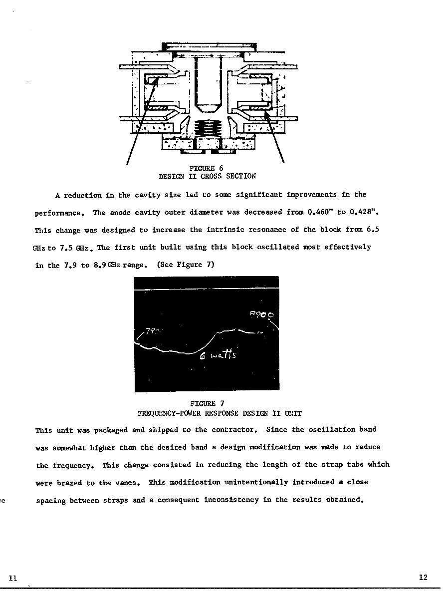
A reduction in the cavity size led to some significant improvements in the
performance. The anode cavity outer diameter was decreased from 0.460" to 0.428".
This change was designed to increase the intrinsic resonance of the block from 6.5
GHz to 7.5 GHz. The first unit built using this block oscillated most effectively
in the 7.9 to 8.9GHz range. (See Figure 7)
FIGURE 7FREQUENCY-POWER RESPONSE DESIGN II UMIT
This unit was packaged and shipped to the contractor. Since the oscillation band
was somewhat higher than the desired band a design modification was made to reduce
the frequency. This change consisted in reducing the length of the strap tabs which
were brazed to the vanes. This modification unintentionally introduced a close
spacing between straps and a consequent inconsistency in the results obtained.
11 12
'I
3 However, experimental data were obtained from two tubes which provided a further
I insight into the design and operation of the units.
One of the purposes of Design II was to avoid the cathode .oupling which is
r inherent in interdigital type circuits. However, the operation of the two tubes
described above indicated that cathode coupling was a significant factor. This
r became apparent as the performance was quite sensitive to vertical position in the
I magnet. By probing the fields in the vicinity of the cold cathode lead the performance
could be changed considerably. By covering the cathode with a shield, the leakage
T could be minimized and the performance enhanced considerably.
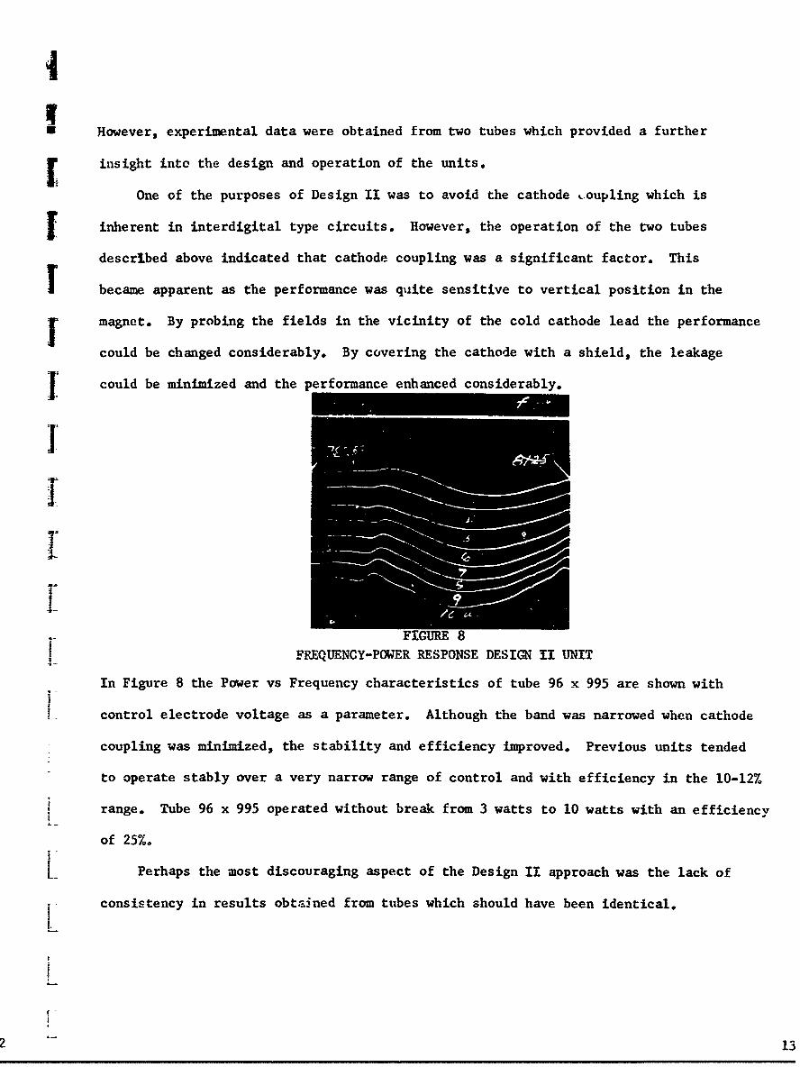
In Figure 8 the Power vs Frequency characteristics of tube 96 x 995 are shown with
II
control electrode Powear s a parameter. Although the band was narrowed when cathode
coupling was minimized, the stability and efficiency improved. Previous units tended
to operate stably over a very narrow range of control and with efficiency in the 10-12%
range. Tube 96 x 995 operated without break from 3 watts to 10 watts with an efficiency
of 25%.
Perhaps the most discouraging aspect of the Design II approach was the lack of
consistency in results obta.ined from tubes which should have been identical.
2 13
During the seventh quarter a total of 21 operable Design ii tubes were Lested,
Some of these tubes incorporated deliberate modifications to improve performance
but many were supposedly identical. It was only possible to speculate why this
design was beset with inconsistency whereas lower frequency VTM's exhibited results
which were quite reproducible. The difficulty could well have arisen from the fact
that the tube is large compared with a wavelength - a presumed advantage, incidentally,
at the beginning of the program. As discussed in the Seventh Quarcerly Report, the
field configurations and interactions may be much more sensitive to abberations in
the tube structure. Also, the large diameter which isolates external circuitry from
the interaction may lead to extreme sensitivity in the coupling schemes. X-ray data
and examination of a number of tubes which had been destroyed for study indicated
that the difficulty in reproducing results was due to a very subtle and undetermined
cause,
In Table I the composite data for all Design II tubes is presented. Of the
total of 43 tubes built 41 were operable. Of the operable tubes a total of 9 tubes
exhibited wide band performance which could be considered interesting. Although
these isolated results illustrated that the basic design was feasible, the yield of
satisfactory packages was distressingly low.
In view of results being obtained with a modified Design I approach, to be
described below, the effort on Design II was terminated at the end of the seventh
quarter. It is quite possible that the approach of Design II would be superior if
further development were continued. This is particularly true if frequency bands above
8 Gc were of interest. At least two of the concepts which evolved during the subsequent
Design I program could be applied beneficially to the Design II approach, a reduction
in the axial vane length and a cavity enclosure for the cathode button. Also,
modifications of the control electrode and cathode geometries would likely improve
performance.
13 14
FThe significant results of this phase of the program can be summarized by the
r following observations:
1.) Wide band, stable performance was demonstrated indicating that themethod of disc strapping and coupling is practical.
2.) Mode stability of the disc strapped structures was found to beexcellent. At no time was the limiting factor mode stability.
3.) Operating efficiency of 257% over a wide band was observed indicatingthat the disc coupling scheme was capable of providing effectivej• loading of the interaction.
4.) Several watts were obtained in a stable oscillation in the 8 to 9 Gcband indicating promise of this approach at higher frequencies.
The problem areas which remain in any further development of the Design II
I approach may be summarized as follows:
1.) Inconsistency of results from "identical" tubes. The solution hereT must lie in extreme care in both tube fabricatlon, parts and procedures.I as well as in precise control of external circuitry.
2.) Cathode coupling. This condition may be minimized by a combination
r of internal geometry changes and external circuitry to choke thecathode circuit and prevent external coupling.
F 3.) Back heating of the emitter. This characteristic was common to allF: of the operating Design II units. No extensive development was under-taken to minimize the effect. It was noted, however, that as cathodecoupling effects were minimized, back heating characteristics improved.A similar study of control ring coupling should provide further im-provement in this area.
4.) External Circuit Design. Much work remains to be done to optimize thecircuitry associated with Design II units. It is likely that moreprogress could be made in a coaxial configuration with a later transitionto waveguide.
LI-FL
I-"
III DESIGN I PROGRAM
The performance of wide band lower frequency VTM's has given an insight into the
problem of mode interference. (See Appendix V for discussion.) The mode problem would
be avoided if it were possible to frequency-scale a satisfactory lower frequency unit.
This, however, is not practical if the same tolerances prevail and if anode voltage is
to be held to a reasonable value. Two concepts were applied to the Design I in order
to insure an effective interaction area and mode stability. The first was to maintain
the extended vane length in order to avoid power limitations which had been indicated
during previous experience. The second was a unique strapping arrangement which would
insure mode stability in spite of the extended vanes.
A cross section view of Design I is shown in Figure 11.
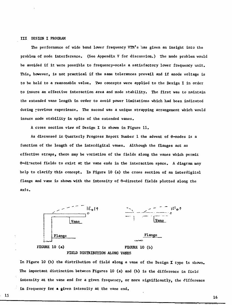
As discussed in Quarterly Progress Report Number 1 the advent of e-modes is a
function of the length of the interdigital vanes. Although the flanges act as
effective straps, there may be variation of the fields along the vanes which permit
e-di-ected fields to exist at the vane ends in the interaction space. A diagram may
help to clarify this concept. In Figure 10 (a) the cross section of an interdigital
flange and vane is shown with the intensity of 0-directed fields plotted along the
axi s.
Flange Flange
FIGURE 10 (a) FIGURE 10 (b)
FIELD DISTRIBUTION ALONG VANES
In Figure 10 (b) the distribution of field along a vane of the Design X type is shown.
The important distinction between Figures 10 (a) and (b) is the difference in field
intensity at the vane end for a given frequency, or more significantly, the eifference
in frequency for a given intensity at the vane end.
15 16
I
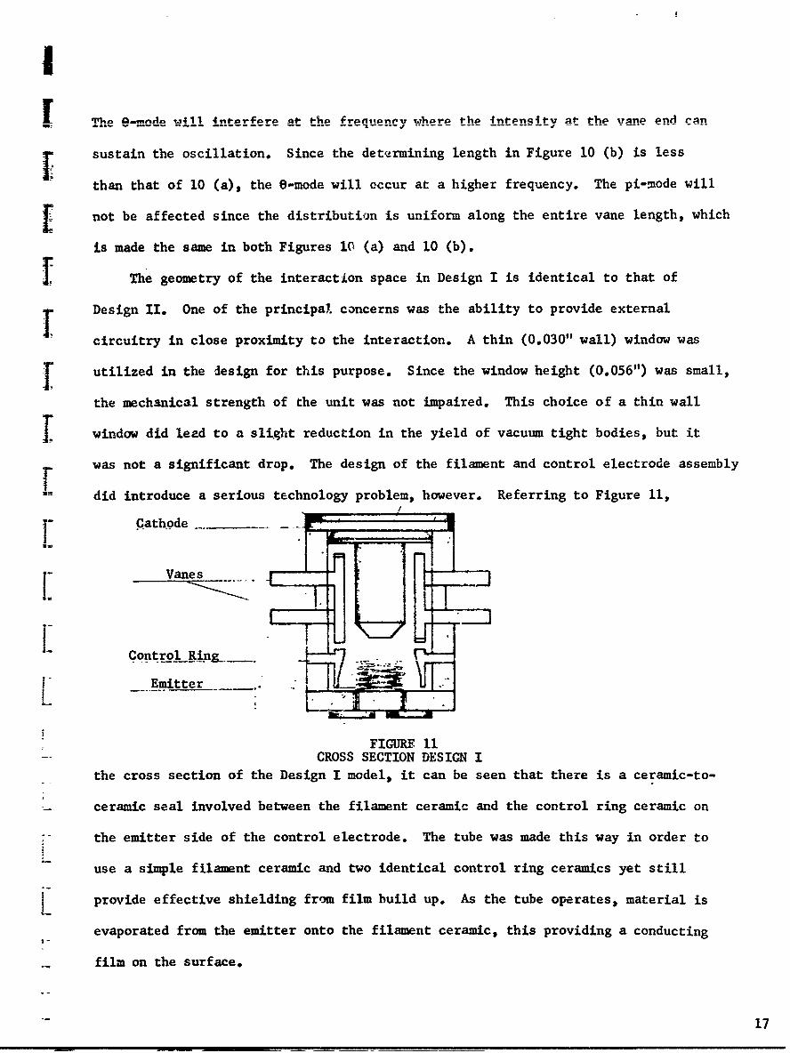
i sustain the oscillation. Since the determining length in Figure 10 (b) is less
than that of 10 (a), the 0-mode will "ccur at a higher frequency. The pi-mode will
[ not be affected since the distribution is uniform along the entire vane length, which
is made the same in both Figures l0 (a) and 10 (b).
IIThe geometry of the interaction space in Design I is identical to that of
r Design 1I. One of the principal concerns was the ability to provide external
circuitry in close proximity to the interaction. A thin (0.030" wall) window was
T utilized in the design for this purpose. Since the window height (0.056") was small,
the mechanical strength of the unit was not impaired. This choice of a thin wall
S window did lead to a slight reduction in the yield of vacuum tight bodies, but it
was not a significant drop. The design of the filament and control electrode assembly
did introduce a serious technology problem, however. Referring to Figure 11,
Cath-ode __ -
Vanes
Iii Control Ring
I- Emitter ___._
FIGURE 11CROSS SECTION DESIGN I
the cross section of the Design I model, it can be seen that there is a ceramic-to-
ceramic seal involved between the filament ceramic and the control ring ceramic on
the emitter side of the control electrode. The tube was made this way in order to
use a simple filament ceramic and two identical control ring ceramics yet still
provide effective shielding from film build up. As the tube operates, material is
evaporated from the emitter onto the filament ceramic, this providing a conducting
film on the surface.
17
Hiowever, the design provided excellent shielding behind the projection oL the control
ring and thus a continuous film between emitter and control electrode could not exist.
The difficulty arose when a metallic ring was used to facilitate the ceramic-to-
ceramic seal. When the external connection was made between the control electrode
and the button on the filament ceramic, the shielded path was shorted and conducting
film became a problem. This connection is usually made by painting a conducting
stripe from the control electrode to the button. Attempts were made to by-pass the
metal ring between ceramics with a tantalum tab, but this was difficult to attach to
the control electrode. Also, the tab projected outward and introduced voltage break-
down problems. The solutions to thz problems introduced by the ceramic-to-ceramic
seal in the design were not solved until the two ceramics were replaced by a single
ceramic. This will be described in more detail during the discussion of the modified
(short) Design I tubes.
A total of 17 Design I tubes was built. These are tabulated in Chart II with
indications of the geometrical distinctions and the performance characteristics.
Almost without exception, the performance of these units yielded no significant
positive results. One unit (93-782) was operated over a 900 Mc hand around 7.5 Gc
and produced about 8 watts in a stable oscillation. It was determined, however, that
the tube was oscillating in a 6-mode. This determination was made by observing the
voltage and frequency characteristics of other modes which were present. Tube 93-782
was, incidentally, a 16 vane tube. The efficiency of the oscillation was less than
10%. Consequently, no attempt was made to pursue this type of performance.
The progress of the Design I approach was limited by several factors, some of
which were later found to be of a fundamental origin and irberent in the design
approach. At the end of the seventh quarter, the results of this approach were
negligible and the entire effort was to be directed to Design II approach. The
problem areas of the Design I approach can be summarized as follows:
.7 18
!
1.) Tubes which generated film due to the design of the filamentceramic assembly had very limited life because heat get.iratedwith the film current cracked the ceramic.
2.) Tubes which did oscillate for brief periods cculd not be loadedeffectively. The heater characteristics indicated severe backheating even though no external evidence of oscillation was present.It was suspected that the tubes were oscillating in a 0-mode andin a circuit contained within the vacuum envelope. This type ofbehavior always led to the destruction of the tube because of theheat generated internally.
I The Design I approach would have been abandoned as u.nsatisfactory if it had
not been for some significant results obtained from other programs which were being
I• conducted at the time. These results will be discussed in detail in the following
section. However, the conclusion of the results, was that the basic concept of
Design I was faulty. In view of this the lack of performance became more under-
f sstandable.
tI
1!I
Il
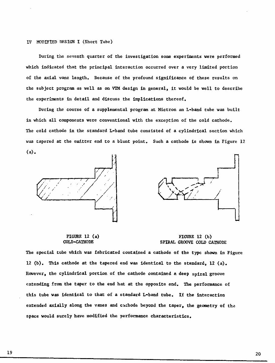
1V .MODIFI!ED DESIGN I (Short Tube)
During the seventh quarter of the investigation some experiments were performed
which indicated that the principal interaction occurred over a very limited portion
of the axial vane length. Because of the profound significance of these results on
the subject program as well as on VTM design in general, it would be well to describe
the experiments in detail and discuss the implications thereof.
During the course of a supplemental program at Mictron an L-band tube was built
in which all components were conventional with the exception of the cold cathode.
The cold cathode in the standard L-band tube consisted of a cylindrical section which
was tapered at the emitter end to a blunt point. Such a cathode is shown in Figure 12
(a).
FIGURE 12 (a) FIGURE 12 (b)
COLD-CATHODE SPIRAL GROOVE COLD CATHODE
The special tube which was fabricated contained a cathode of the type shown in Figure
12 (b). This cathode at the tapered end was identical to the standard, 12 (a).
However, the cylindrical portion of the cathode contained a deep spiral groove
axtending from the taper to the end hat at the opposite end. The performance of
this tube was identical to that of a standard L-band tube. If the interaction
extended axially along the vanes and cýichode beyond the taper, the geometry of the
space would surely have modified the performance characteristics.
19 20
I.fA second experiment which substantiated the above-described results involved
F- tubes having different angles on the tapered sections of the cathodes. The anode
voltage for a given frequency was directly related to the taper and essentially
I: independent Qf the principal cathode diameter, the inference again being that the
interaction occurs in the region of the vanes closest to the emitter. There are,
F of course, effects of the cathode post geometry on the composite electromagnetic
I fields in the interaction space, and these will indirectly affect the interaction.
An example of this would be the cathode-anode capacitance itself,
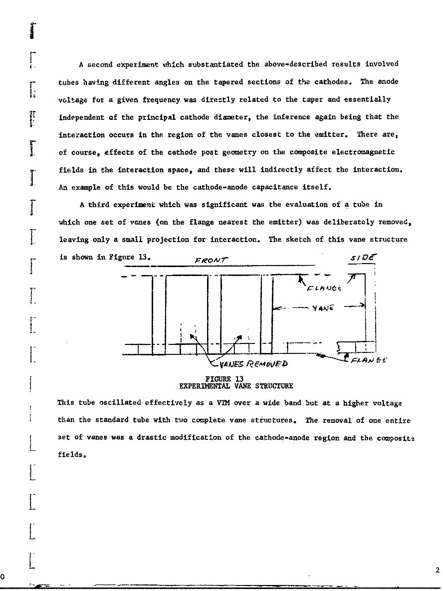
A third experiment which was significant was the evaluation of a tube in
which one set of vanes (on the flange nearest the emitter) was deliberately removed,
I leaving only a small projection for interaction. The sketch of this vane structure
is shown in Figure 13. FROA"7D
gL/nAJ C- t
FIGURE 13EXPERIMENTAL VANE STRUCTURE
This tube oscillated effectively as a VTM over a wide band but at a higher voltage
than the standard tube with two complete vane structures. The removal of one entire
set of vanes was a drastic modification of the cathode-anode region and the composite
fields.
i-
20
-
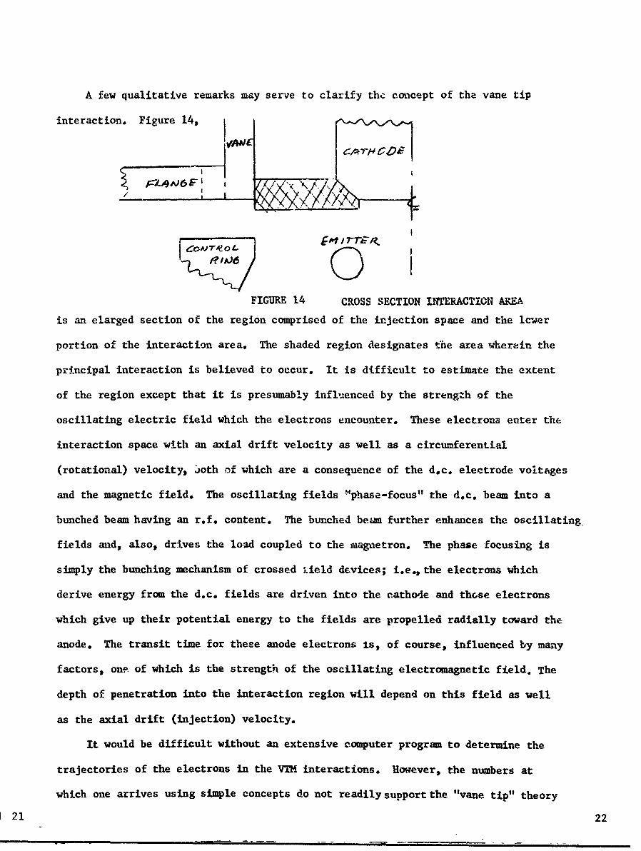
A few qualitative remarks may serve to clarify the concept of the vane tip
interaction. Figure 14,
/ _ _ _
P i 7 ri © ,FIGURE 14 CROSS SECTION INTERACTION AREA
is an elarged section of the region comprised of the injection space and the lc-wer
portion of the interaction area. The shaded region designates the area wherein the
principal interaction is believed to occur. It is difficult to estimate the extent
of the region except that it is presumably influenced by the strength of the
oscillating electric field which the electrons encounter. These electrons enter the
interaction space with an axial drift velocity as well as a circumferential
(rotational) velocity, 3oth of which are a consequence of the d.c. electrode voltages
and the magnetic field. The oscillating fields "phase-focus" the d.c. beam into a
bunched beam having an r.f. content. The bunched beam further enhances the oscillating
fields and, also, drives the load coupled to the magnetron. The phase focusing is
simply the bunching mechanism of crossed iield devices; i.e., the electrons which
derive energy from the d.c. fields are driven into the cathode and those electrons
which give up their potential energy to the fields are propelled radially toward the
anode. The transit time for these anode electrons is, of course, influenced by many
factors, one of which is the strength of the oscillating electromagnetic field. The
depth of penetration into the interaction region will depend on this field as well
as the axial drift (injection) velocity.
It would be difficult without an extensive computer program to determine the
trajectories of the electrons in the VTM interactions. However, the numbers at
which one arrives using simple concepts do not readily support the "vane tip" theory
21 22
I
I in any quantitative measure. The modulation index (ratio of ocillating field
I to d.c. field), based on experimental power and impedance measurements, indicates
that the oscillating voltage is the order of 5% or less of the d.c. voltage at the
F power levels and frequencies under consideration. The unknown quantity is the
magnitude of the axial drift velocity. No experimental or analytical program
I was undertaken to determine these trajectories.
It has been stated that the concept of Design I was faulty in view of the
experimental evidence cited above. It is important to note that excess vane length
I is not only unnecessary but extremely deleterious to the VTW performance. The
effect of vane length on mode stability has been discussed previously in this report
and will not be repeated here. A further degradation in performance arises from a
fundamental relationship involving a figure of merit fo:" all microwave tubes,
klystrons, traveling wave tubes, triodes, as well as magnetrons. Mathematically,
the relation is stated as:
00
.[ r
This expression states that the impedence (or real part thereof) integrated over
f the bandwidth is inversely proportirnal to the capacitance which is associated with
the interaction. Although this theorem has general implications in the areas of
network analysis and synthesis, it is most significant in the design of electronic
devices. The relation is often expressed implicity in stating that well designed
L microwave tubes mlnimize the energy storage in electric fields which do not have
access to the electron beam. For example, consider two segments of a tunnel forming
an interaction gap for a linear beam klystron or traveling wave tube. The theorem
above would dictate a higher intrinsic impedance-bandwidth product for a thin-walled
tunnel than for a thick wall tunnel.
S H. W. Bode Network Analysis and Feedback Amulifier Design. Van Wostrand, New York.
(1945) Page 282.
23
n- fo^ r t ^aa- 4" nn4nt- thp intprdfiatal magnetron VTM performance would degrade
iL the radial thicknees of the vanes were increased. Excess capacity has been
introduced but the fringing fields which interact with electrons would remain un-
changed. Some capacity is obviously necessary to sustain the interaction fields
and the minimum limit is usually set by thermal considerations. In conventional
magnetrons in which the entire cathode emits, excess length introduces extra capacity
but extra electrons are also introduced and the impedance-bandwidth product reduction
will be compensated by a lower electronic impedance.
In the original Design I tubes the extra vane length, considered in the design
concept to be necessary, presented excess capacity which actually degraded the
impedance-bandwidth capabilities of the device. In view of the foregoing considerationsý,
these tubes were redesigned to investigate the behavior of tubes having a shortened
interaction length. The vanes were shortened by the amount that the vane tips
projected beyond the flange. This resulted in a conventional interdigital type
structure having a short interaction length. The length of the vanes was reduced
from 0.170" to 0.116"1, a 32% reduction. Reducing the height of the tube resulted
in a bonus advantage which was not a consideration in the design. The overall
height of the tube was reduced from 0.468" to 0.376" permitting a corresponding
decrease in the magnet gap. This is more than a marginal improvement since it leads
to approximately a 507. reduction Ln weight for the same field strength.
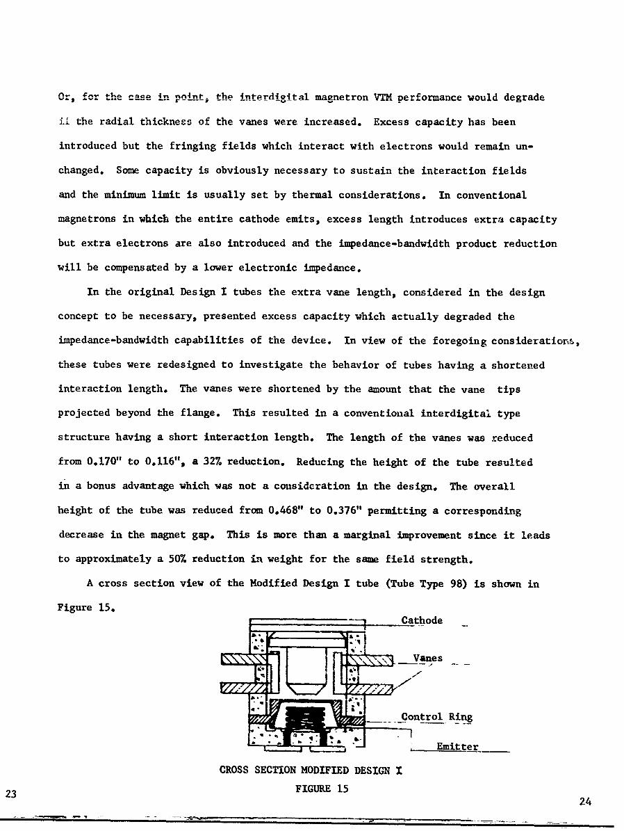
A cross section view of the Modified Design I tube (Tube Type 98) is shown in
Figure 15.
Cathode
Control Ring
Si Emitter
CROSS SECTION MODIFIED DESIGN X
23 FIGURE 15 24
014
0 4
oto
An additional improvement was incorporated in the design as Type 98 tubes were
j being assembled. A new filament ceramic had been procured which permitted excellent
shielding from products emanating from the emitter. Figure 15 (a) is a photograph
of an assembled tube with a layout of components parts.I
In order to facilicate the circuit development, the Type 98 units were
installed in coaxial-type circuits rather than in waveguides. The initial test
results were the most promising of any obtained to that point in the program.
During the eighth quarter, a total of twenty three type 98 tubes were built.
f (Before the design was standardized, this type was designated as 93x.) Seventeen
of the units were operable and five of these exhibited excellent performance. Some
of the more significant results are tabulate, below.
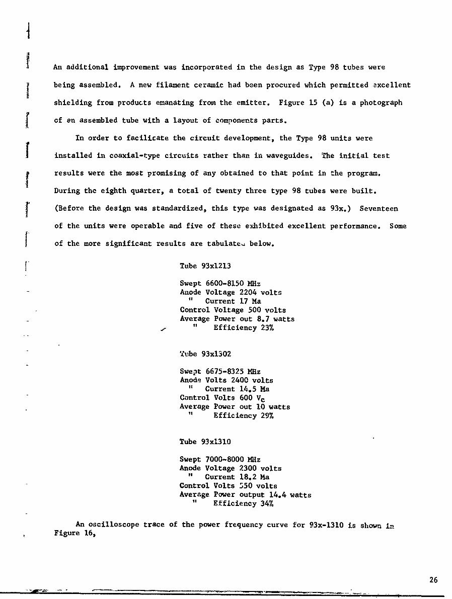
Tube 93x1213
Swept 6600-8150 NHzAnode Voltage 2204 volts
" Current 17 MaControl Voltage 500 voltsAverage Power out 8.7 watts
Efficiency 23%
jube 93x1302
Swept 6675-8325 MHzAnode Volts 2400 volts
" Current 14.5 MaControl Volts 600 VCAverage Power out 10 watts
"i Efficiency 29%
Tube 93x1310
Swept 7000-8000 MHzAnode Voltage 2300 volts
" Current 18.2 MaControl Volts 550 voltsAverage Power output 14.4 watts
" EffIciency 347.
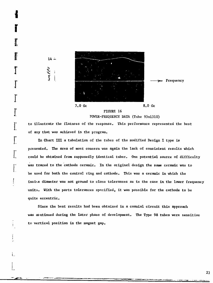
An oscilloscope trace of the power frequency curve for 93x-1310 is shown inFigure 16,
26
IIr
I14
r .. - => Frequency
7.0 Gc 8.0 Gc
j FIGURE 16POWER-FREQUENCY DATA (Tube 93x1310)
"f to illustrate the flatness of the response. This performance represented the best
of any that was achieved in the program.
1| In Chart III a tabulation of the tubes of the modified Design I type isI-
presented. The area of most concern was again the lack of consistent results which
L• could be obtained from supposedly identical tubes. One potential source of difficulty
was traced to the cathode ceramic. In the oziginal design the same ceramic was to
be used for both the control ring and cathode. This was a ceramic in which the
insikýe diameter was not ground to close tolerances as is the case in the lower frequency
units. With the parts tolerances specified, it was possible for the cathode to be
quite eccentric.
Since the best results had been obtained in a coaxial circuit this approach
was continued during the later phase of development. The Type 98 tubes were sensitive
to vertical position in the magnet gap.
2-
As was found in the case of Design II units, t'L phcn=Cnn was a circuit effec..t
rather than an electronic effect. Energy was being coupled out via the cathode
making the magnet an effective part of the circuit. A solution to this problem
was achieved by creating a cavity around the cathode button. A section of the
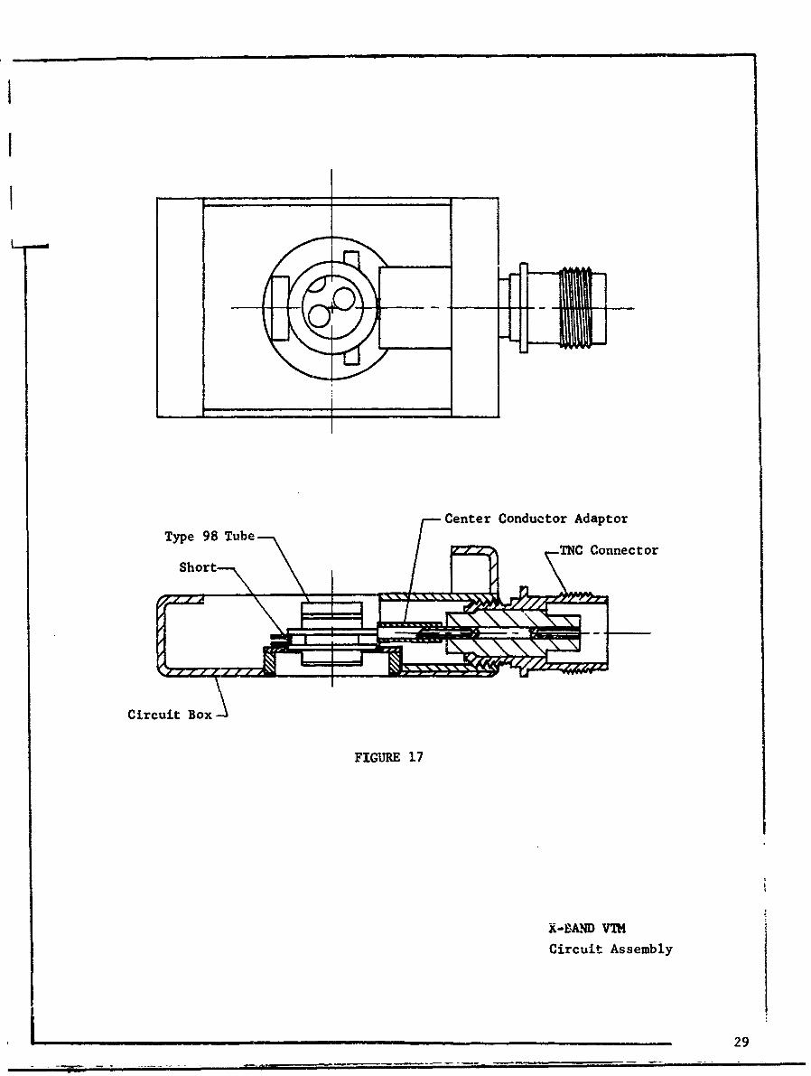
circuit assembly is shown in Figure 17. The lower flange of the tube is soldered
to the circuit base and the cathode electrode is recessed in the lower cavity.
Beryllium copper tuning shorts are positioned around the tube window and soldered
into place after adjustment, The top tube flange is coupled directly to a matching
slug which has been soldered to the center conductor of the screw-in TNC connector.
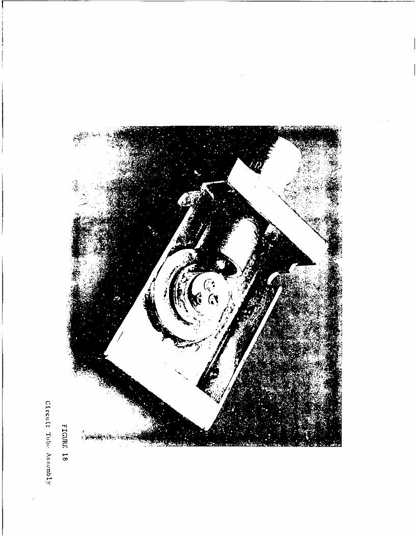
A photograph of a tube, circuit, and output connector is shown in Figure 18.
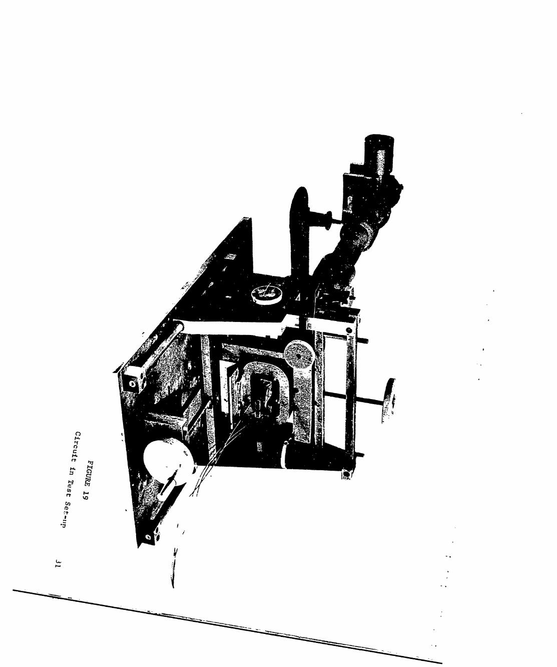
Figure 19 shows the tube-circuitry assembly mounted with the test equipment and
the magnet alignment jig.
There were problems of instrumentation associated with the coaxial circuitry
at the frequencies of interest. Furthermore, the objective specifications called
for RG 51/U waveguide output. None of the coaxial attenuators which were available
would handle the power above 5.0 Gc. When a directional coupler and matched
termination were used, the mismatch (1.3 VSWR) affected the performance of the VTM.
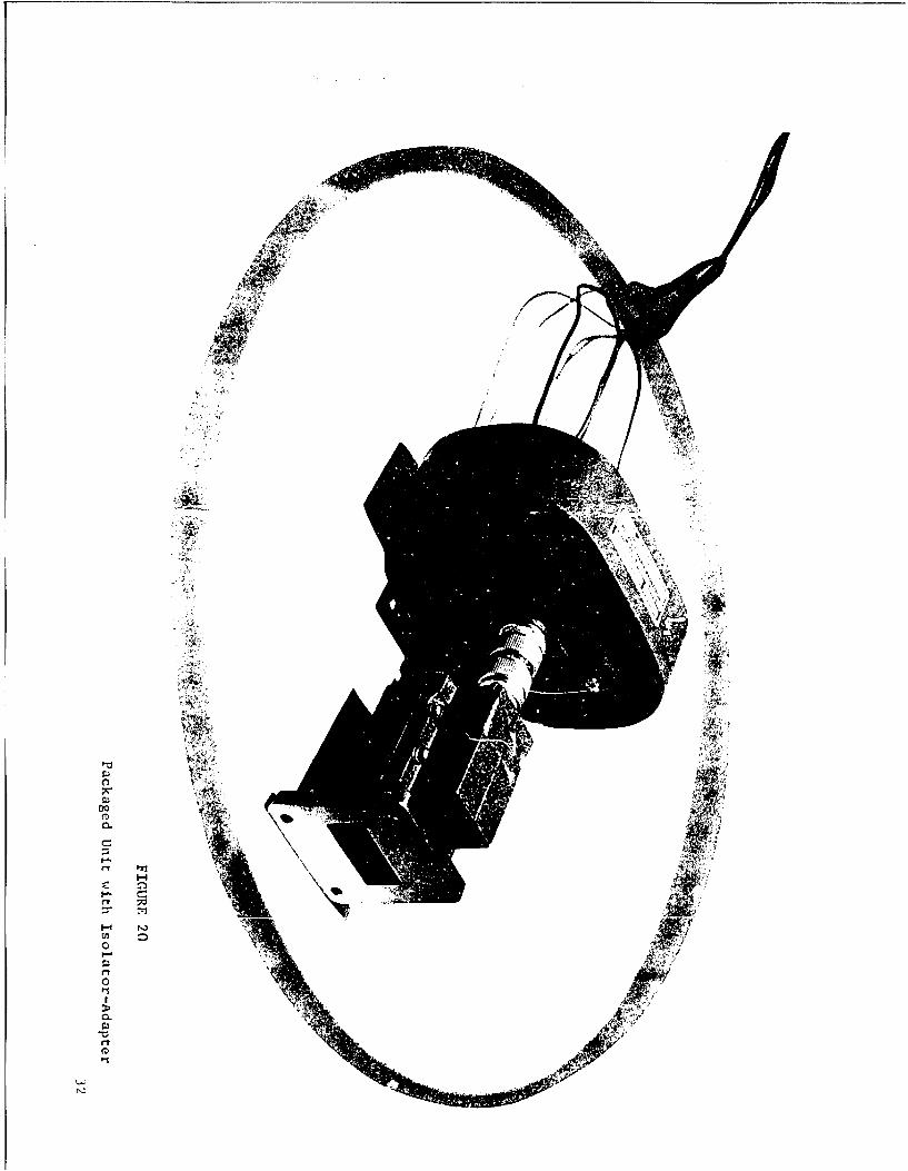
During the eighth quarter, a 10 watt isolator, which also served as a TNC to RG 51/U
adapter, was obtained. This facilitated the instrumentation and also improved the
performance of the VTV because of the improvement in the termination input VSWR.
A photograph of a packaged unit showing the isolator is shown in Figure 20.
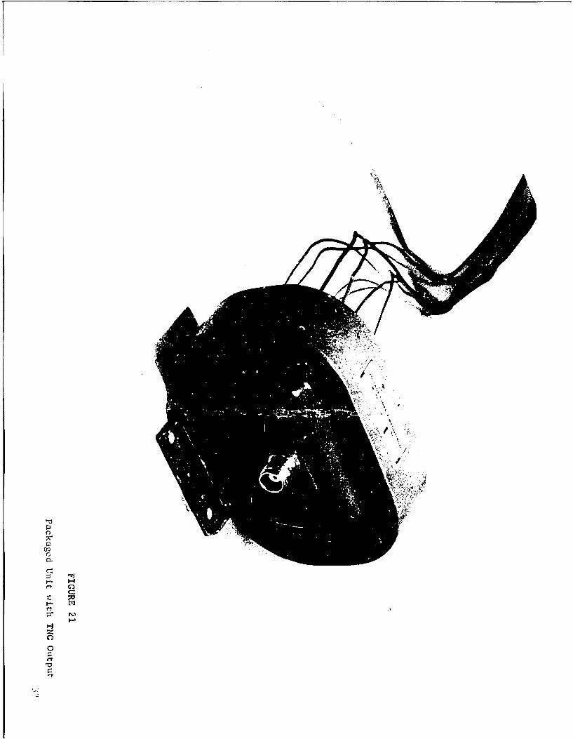
Figure 21 is a photograph of a packaged unit without the isolator adapter.
The effort during the final phase of the program was devoted to the following
areas:
1.) Standardization of tube design.
2.) Consistency of results.
3.) Improvement of back heating ratio.
4.) Potting and packaging.
5.) Delivery of units required by contract.27
28
I'I ~1
Center Conductor Adaptor
Type 9 TubeTNC Connector
Circuit Box
FIGURE 17
X-)DAND VTh
Circuit Assembly
1 _____29
cn co
I"'
0
M.
*.�. H�
f-..�0
a
V
rr hTi
Ali
0n
C,
ri
(D
0
C-
I-. t�Ir? c�
�- ,�3I-.
H
0
0
-I.
- Many modifications of the tube geometry had been made during the course of
the program. These were primarily in the cathode and control electrode shapes.
The power, stability, noise and backheating characteristics were observed as various
combinations were evaluated. The geometry was finally standardized with theI
dimensions of the units which had yielded the best overall performance. The
significant feature of the cathode design was a very short taper section as can
be seen from the Modified Design I (Type 98) section of Figure 15. Best results
were obtained from tubes which had a 0.160" diameter control electrode with a
slight taper. The anode structures were interdigital units having 9 vanes on
each flange. The emitter was a thoriated tungsten filament with an O.D. of 0.110".
34
1i~
a -!-- - -o
I
5 The problem of inconsistent results from "identical" tubes was approached from
both the tube and the circuit aspects. A rigorous quality control was initiated to
follow the tube components through fabrication, processing, and assembly. The anodle
[ blanks were carefully measured prior to EDM and the vane structures were checked
after their return. All metal parts and ceramics were carefully measured and those
not meeting specified tolerances were rejected. All tubes were assembled and brazed
using the same fixtures in order to eliminate this as a variable. The sub-assemblies
were checked under a microscope for any abberations which could be observed. The
f fabrication of these units represented what was considered the best practical procedure
which could be used.
j A standard circuit (as shown in Figures 17 and 18) was used to evaluate the tubes.
There were still variations possible in the exact geometry of the coupling slug and
I the exact placement of shorting tabs around the periphery of the window. These
variables, however, were adjusted for optimum performance with each tube. The results
of testing tubes during this phase of the program will be discussed below.
Back-heating caused by electrons driven from the oscillating fields into the
emitter is a major factor in the life of a VTM. The problem is particularly severe
L in wide band VTM's where back heating may depend on the frequency (voltage). If
the emitter temperature is adjusted to accomodate the back heating at one end of the
band where it is most severe, the emission may be inadequate at the frequencies where
back heating may be less of a factor.
Two significant observations were made concerning back heating in the tubes of
the subject program. First, there appeared to be a direct correlation between the
degree of back heating and the diameter of the control electrode. Tubes were built
which were identical except for this parameter and the back heating was most severe
L in those having the smallest diameter. The second observation was that the degree
of back heating was inversely dependent on the general tube performance. The units
L in which the lowest back heating characteristics were observed also exhibited the
best frequency, power and efficiency characteristics.
L 35
A possible explanation of this correlation concerns the amount of r.f. which couples
into the control electrode circuit. The effect of the potting compound on performance,
to be discussed below3 also substantiates the evidence that r.f. is prevalent in this
area. An oscillating field superimposed on the d.c. fields at the emission surface
would result in severe back heating of the emitter as well as in a general degradation
of performance. A solution to this problem will be suggested in the portion of the
report containing conclusions and recommendations for further development.
As the electrical performance was achieved more effort was devoted to packaging
the units in a manner which would be compatible with environmental requirements of
the specifications. Since the basic approach did not differ from that of the standard
Mictron lower frequency units, no extensive modifications were considered necessary.
Units had been built which had been qualified for military systems with rigorous
vibration, shock, altitudes temperature and humidity requirements. A discussion of
this procedure may be found in Appendix VI.
One problem, unique to the X-Band development, did arise, however, during the
potting operation. Tubes are frequently tested with a layer of insulating tape as
a temporary measure to prevent breakdown. Before the tube-circuit is packaged, this
tape is removed and a liquid silicone rubber potting compound is applied to cover
the external tube electrodes and connecting leads. This procedure insures that
voltage breakdown does n-t occur between the electrodes even at the reduced pressures
of high altitude. There are many varieties of silicone rubber compound which may
be generally suitable for potting, but many of these were not satisfactory for the
X-Band units.
The effect of the potting compound on performance was most pronounced at the
high frequency end of the spectrum. The effect on a typical power-frequency spectrum
is illustrated in Figure 22.
36
I
rA
FIGURE 22EFFECT OF POTTING ON FREQUENCY CHARACTERISTICS
T Since other factors appeared to be limiting the high frequency response, the effect
of the potting was even more severe. The time available did not permit an extensive
program to investigate this phenomenon but an interim solution was obtained by
I selecting the best of the available compounds and applying it sparingly. Even at
best, however, the high frequency was significantly degraded. The preferred potting
j.Y compound was found to be General Electric Clear Silicone Potting Compound RTV-602.
The VTM test data sheets for the six experimental models which were delivered
are contained in Appendix III. The tubes used in these packages were all Type 98
tubes mounted in the same basic circuit. There were, however, minor differences in
the coupling circuitry. A few comments regarding the performance data are in order.
The best performance data was achieved with Model 1OX7-8 Serial Number 2 which
incorporated Tube Number 98x-1660. This tube oscillated from 6800 MHz to 8050 MFz
- with an average power of 10.8 watts and an efficiency of 33.3%. The anode voltage
ranged from 2170 to 2515 volts. The back heating on this tube was minimal and the
control range and stability were also good. The tube itself would be considered as
L the basic design unit from which to proceed with any further development.
It can be seen from the experimental data that most of the units were defic4 ent
L at the high frequency end of the spectrum. Suggestions will be made in a later
L section to improve this situation and extend the frequency range and bandwidth
capability.
_37 -V - -
Also, it will be noted that units 3, 4, and 6 indicate that performance is sensitive
t heater current. These are units which suffer from a combination of back heating
effect and limited control range.
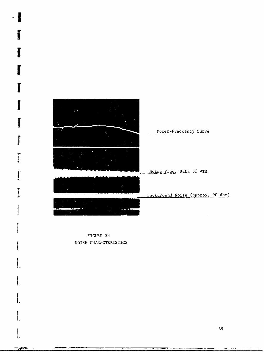
Although the noise characteristics were of interest no intensive effort was
made to improve the performance in this respect. The noise response of 1OX7-8
#3 is shown in Figure 23. This oscilloscope picture is cypical of the response of
the units. During the interim development, however, units were tested which were
significantly better, indicating that improvement in this area could be expected.
The noise was measured by means of a wide band crystal mixer and an amplifier with
a band of I00 KHzto 100 MHz. The tube was swept over its operating range as noise
was measured. Since the oscilloscope had an amplifier with a I0MHzresponse, the
noi3e presented was that which occurred in a band from 100 Kc to 0 1MHz around the
carrier as it was swept. The trace at the bottom of the photograph of Figure 23
illustrates the relative magnitude of the system noise in the absence of the VTM
signal. The VTM level is adjusted until the reference noise level is doubled.
Under these conditions the noise level measured was the order of 80 db below the
carrier over the 7 to 8 GHz band.
During the final phase of the program some effort was devoted to inveatigating
tubes designed to extend the frequency range. Although the development did not
produce any positive results, some comments may be pertinent. A few tubes of the
Modified Design I type having 10 vane anodes were constructed from the blanks for
9 vane anodes. These units, 6perated in a coaxial circuit- did not oscillate well
in the specified band but did produce several watts in a narrow band around 9.4 GHz.
In view of the foregoing discussion on the effects of capacity on performance it
would be expected that these units would be inferior. Furthermore, the difficulty
in assembling these units with this corresponding close vane spacings precluded
any extensive effort to continue with 20 vane tubes.
3738
--I-e--rqecyCre
]I
[I.I
I+S+ ___Power_-Frequency Curve.
I
__Noise Freq. Data of VTM
_ _3ackground Noise (approx. 90 dbm)
I
FIGURE 23
NOISE CHARACTERISTICS
I3! 39
il
The second tube type which was investigated during the late phase of the
program contained an emitter and cathode of 0.075" diameter and anodes of 0.140"
diameter. The choice of these dimensions was dictated primarily by the availability
of the 0.075"emitter and a filament ceramic which would accommodate it. The anode
diameter was chosen to give an operating voltage of the proper magnitude. Several
units of this type were built and none oscillated at any frequency. It became
apparent that the anode-cathode diameter ratio was too large to permit the start
of oscillations. This investigation was discontinued as the effort was concentrated
in the areas where positive results had been demonstrated.
40
w• m mw • w----------------

I
I 'OVERALL SUMMARY AND RECOMMENDATIONS
f During the course of the program a total of 136 tubes of all types were
fabricated. Of these tubes, 118 were operable to the extent that they were tested
F in r.f. circuits. Of the operable tubes, 41 were of Design II type, 15 were Design
I, 37 were Modified Design I (short tubes) and the remaining 25 were miscellaneous
types having 6, 7, 8 and 10 vane anodes. This latter group of tubes was used in
preliminary development work and for evaluation of higher frequency designs.
Although many promising results were obtained with the Design II approach,
f the lack of consistent results defeated the attempt to achieve contract specifications.
This characteristic was ascribed to the sensitivity of the performance to slight
i abberations in the internal tube geometry and the external circuitry, being a
consequence of the relatively large electrical size of the unit. Other problem
areas associated with the Design II approach were concerned with the relative
I complexity of the unit as compared with the interdigital design, the consistently4-
low efficiency which was observed in operating units, and the excessive back heating
of these units. The Design II approach would warrant further investigation in any
L program to achieve performance in higher frequency bands. In this case, a more
sophisticated approach to coupling and external circuitry would be suggested. The
positive aspects of this phase of the program include the demonstration of a unique
method to achieve mode stability and symmetrical coupling over a wide band of
frequencies.
The original Design I approach did not yield any meaningful results of a
positive nature. However, as the course of the investigation revealed that the
L concept of the extended interaction length was detrimental, this vehicle served as
a basis for designing shorter tubes which did perform effectively. Also, technology
problems, common to both interdigital types, were solved using the components of
the original Design I units. No further investigarion of this particular approach
is suggested.
41
Although the 0-mode approach was designated at the outset of the program to
merit careful consideration, the performance which was observed never warranted
more than a cursory investigation. (See Appendix VII for a discussion of 0-mode
operation.) During the early phase of the program several tubes were built in
an attempt to enhance 0-mode performance. Although these units could be made to
oscillate over sulstantial bands, the stability and efficiency in all cases were
found to be marginal. This effort was discontinued as Design I and Design II
units became available and exhibited more interesting performance oscillating in
pi-mode. No recommendations regarding further effort on the e-mode approach will
be made because of the limited experience in this area during the program.
A modified Design I approach in which the anode length was reduced by 32%
provided the best results during the program and the best promise for further VTM
activity in the X-Band frequency range. Although the effort was plagued by an
inability to achieve consistent results, units were obtained which exceeded
-portions of the electrical specifications deliniated by SCL-7001/86 (Appendix I).
An average power of 11 watts was achieved over the 6850-8050 MHz band with a
variation of less than 2db. and an average efficiency of 33%. This performance
was achieved in a unit which exhibited good stability with changes in control
electrode voltage and was not impaired by severe back heating. Many of the units
which were shipped in accordance with contract requirements did not exhibit these
features and also were limited in performance at the high frequenc, end of the
spectrum. However, the causes of these deficiencies are understood and remedies
will be suggested for further development.
Since the performance of the units was found to be marginal in the vicinity
of 8 Tiz and above, a new design should be modified accordingly. In view of the
discussion of the effect of intrinsic capacitance on impedance-bandwidth charac-
teristics, steps should be taken to reduce thi.s parameter.
41 42
IT
Perhaps the most straightforward approach would be to redesign the unit to have
slightly reduced cathode and anode diameters, e.g., a 0.100" diameter cathode with
0.150" anodes This modification should extend the frequency range appreciably.
A slight improvement could be achieved by thinning the radial dimension of the
anode vanes. Thib •,ould reduce the vane-to-vane capacity but not the vane-to-
cathode capacity, both of which limit the impedance-bandwidth product.
A second development suggested to improve performance would be in the .reaI
of reducing r.f. in the region between the emitter and the control electorode.
Following the improvement notee when the cathode electrode was enclosed in a
cavity, a similar arrangement could be provided for the emitter and control
electrodes. Also, modifications of the internal control electrode geometry should
be investigated as a means to eliminate the oscillating fieids from the emitter
surface. Advances in this area could be expected to result in a reduction of back
heating as well as a general improvement in performance.
An extended development should, of course, include refinement of -he external
circuitry-. The characteristics of coaxial plumbing, particularly TNC, at X-Band
are, at best, questionable. From a system standpoint the VTM units should be
designed in waveguid2 circuits. The incorporation of an isolator is strongly
recommended in any event.
As a final recommendation for further development of nigh frequency VTM
units the importance of precision parts with close tolerances should be emphasized
as well as extreme care in the fabrication of tubes and circuits.
43
APPENDIX I
SiQL CORPS SCL-7001/oTECHNICAL 21 November 1962REQUIREMENTS Specifications Amended 3 April 1963
Amendments on page 49CW X-BAND VOLTAGE-1UNABLE OSCILLATOR
1. SCOPE
1.1 This specification covers firm and objective requirementf for thedevelopment of a voltage-tunable oscillator capable of operadion over thefrequen:y range of 7.0 to 8.0 gigacycles (Gc) at a CW power output level of10 wat:s. The following types of oscillators are some suggested approachesto tLs development, but should not be considered as limiting.
(a) Voltage-tunable magnetron
(b) M-type backward wave oscillator
(c) TWT and feedback device
2. APPLICABLE DOCUMENTS
2.1 The following documents, of the issue in effect on date of invita-tion for bids, form a part of this specification to the extend specified herein.
SPECIFICATION
SIGNAL CORPS
SCL-7001/86 Electron Tubes
MILITARY
MIL-E-5400 Electronic Equipment, AircraftGeneral Specification for
(Copies of documents required by contractors in connection with specificprocurement functions should be obtained from the procuring activity or asdirected by Lic contracting officer. Both the title and identifying numberor symbol should be stipulated when requesting copies.)
Sheet 1 of 5 Sheets
43 44
SCL-7001/86 Sheet #2
3. REQUIREMENTS
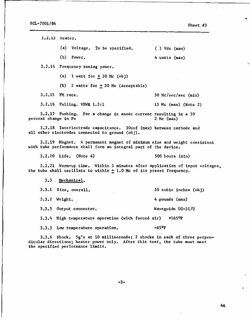
3.1 Description, general. The CW X-band voltage-tunable oscillatorto be developed under this specification shall meet the applicable require-ments of Specific ition MIL-E-l referenced in SCL-70012 , and in addition, thedevice shall have the following electrical and mechanical characteristics.
I 3.2 Electrical.
3.2.1 Frequency. The tube shall be capable of linear voltage tuningwhile meeting the power output requirements over any 60 megacycle band inthe frequency range from 7.0 to 8.0 Gc. (See Note 3)
3.2.2 Power output. 10 watts (min) (Note 5)
3.2.3 Efficiency. 35% (obj); 25% (min)
3.2.4 Anode voltage.
(a) Relative to cathode 2500 V (abs. max)I (b) At center frequency (fo) 2000 V (max)
1 3.2.5 Anode input power. 40 watts (max)
3.2.6 Auxiliary electrode voltage. 1000 V (max), (Note 1)
3.2.7 Auxiliary electrode current. 1.0 ma (max)
3.2.8 Tuning sensitivity. 1.0 Mc/V (min); 4.0 Mc/V (max)
3.2.9 Tuning linearity. Variations of tuning sensitivity shall not bemore than 2 percent (objective) across any 60 megacycle band within the specifiedtuning range.
3.2.10 Power output variation. 4J db (max) over any 60 Mc band within
the specified tuning range of 7.0 to 8.0 Gc. (Note 5)
3.2.11 AM noise.
(a) At lease 90 db below carrier in any 1 Mc band at least5 Mc away from carrier frequency (obj).
(b) 70 db below the carrier in any 1 Mc band at least 5 Me awayfrom carrier frequency (min).
3.2.12 FM noise. 0.1 Mc/Sec (mas) duringnon-mo&ilfated operation.
1--2--
V_- - - _ _ _ _ -
SCL-7001/86 Sheet #3
3.2.13 heater.
(a) Voltage. To be specified. ( ) Vdc (max)
(b) Power. 4 watts (max)
3.2.14 Frequency tuning power.
(a) I watt for + 30 Mc (obj)
(B) 2 watts for + 30 Mc (acceptable)
3.2.15 FM rate. 30 Mc/sec/sec (min)
3.2.16 Pulling. VSWR 1.3:1 15 Mc (max) (Note 2)
3.2.17 Pushing. For a change in anode current resulting in a 10percent change in Po 2 Mc (max)
3.2.18 Interlectrode capacitance. 30uuf (max) between cathode andall other electrodes connected to ground (obj).
3.2.19 Magnet. A permanent magnet of minimum size and weight consistent
with tube performance shall form an integral part of the device.
3.2.20 Life. (Note 4) 500 hours (min)
3.2.21 Warm-up time. Within 5 minutes after application of input voltages,the tube shall oscillate to within + 1.0 Mc of its preset frequency.
3.3 Mechanical.
3.3.1 Size, overall. 30 cubic inches (obj)
3.3.2 Weight. 4 pounds (max)
3.3.3 Output connector. Waveguide UG-51/U
3.3.4 High temperature operation (with forced air) +165 0F
3.3.5 Low temperature operation. -650F
3.3.6 Shock. 5g's at 10 milliseconds; 2 shocks in each of three perpen-dicular directions; heater power only. After this test, the tube must meetthe specified performance limits.
"-3-
46
SCL-7001/86 Sheet #4
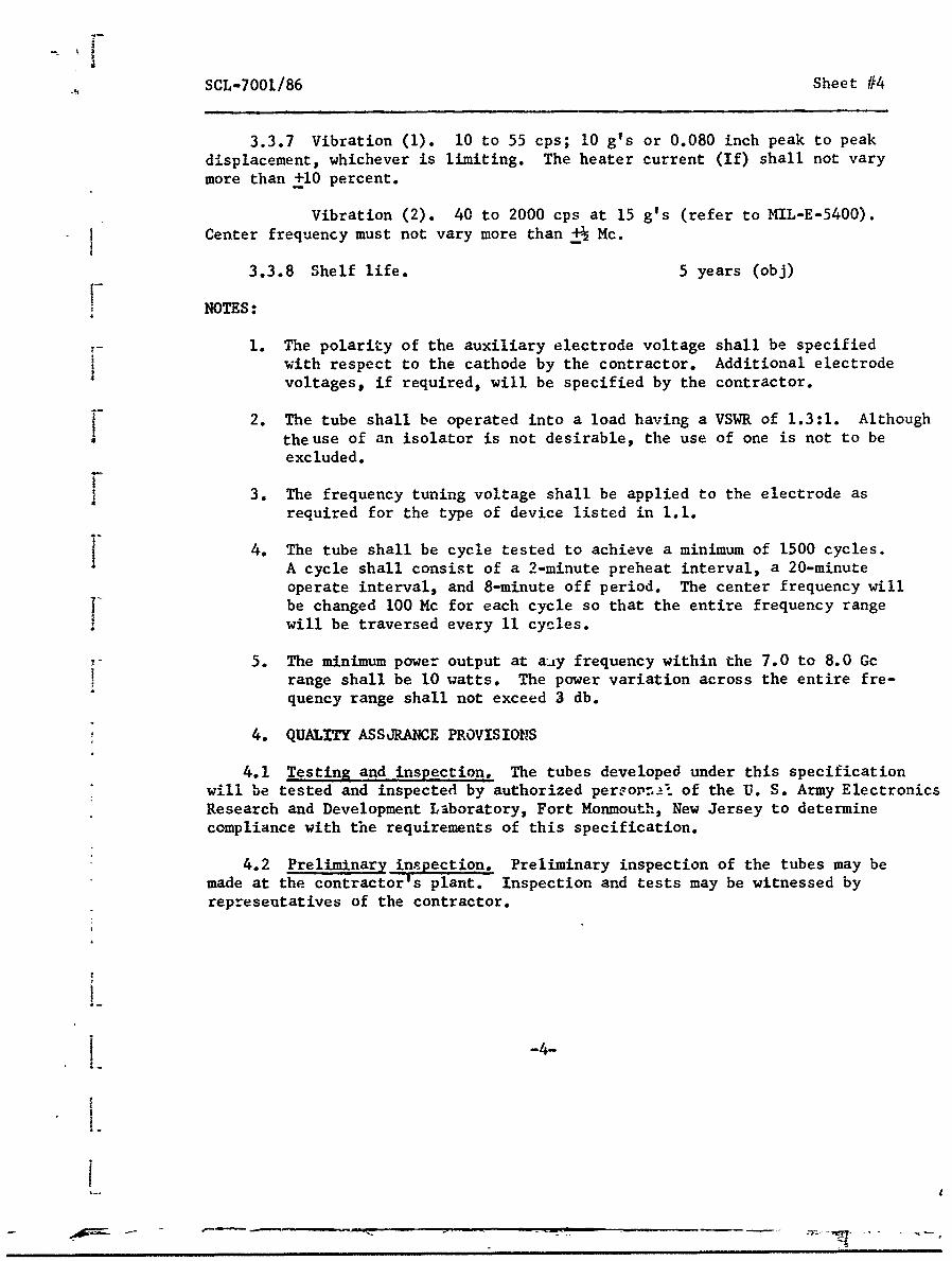
3.3.7 Vibration (1). 10 to 55 cps; 10 g's or 0.080 inch peak to peakdisplacement, whichever is limiting. The heater current (If) shall not varymore than +10 percent.
Vibration (2). 40 to 2000 cps at 15 g's (refer to MIL-E-5400).I Center frequency must not vary more than +± Mc.
3.3.8 Shelf life. 5 years (obj)
F NOTES:
1. The polarity of the auxiliary electrode voltage shall be specifiedI with respect to the cathode by the contractor. Additional electrode
voltages, if required, will be specified by the contractor.
1 2. The tube shall be operated into a load having a VSWR of 1.3:1. AlthoughSthe use of an isolator is not desirable, the use of one is not to be
excluded.
3. The frequency tuning voltage shall be applied to the electrode asrequired for the type of device listed in 1.1.
4. The tube shall be cycle tested to achieve a minimum of 1500 cycles.A cycle shall consist of a 2-minute preheat interval, a 20-minuteoperate interval, and 8-minute off period. The center frequency will
f• be changed 100 Mc for each cycle so that the entire frequency rangewill be traversed every 11 cycles.
5. The minimum power output at a:•y frequency within the 7.0 to 8.0 Gcrange shall be 10 watts. The power variation across the entire fre-quency range shall not exceed 3 db.
4. QUALITY ASSJRANCE PROVISIONS
4.1 Testing and inspection. The tubes developed under this specificationwill be tested and inspected by authorized peroorPe2l of the U. S. Army ElectronicsResearch and Development Laboratory, Fort Monmouth, New Jersey to determinecompliance with the requirements of this specification.
4.2 Preliminaryinecton. Preliminary inspection of the tubes may bemade at the contractor's plant. Inspection and tests may be witnessed byrepresentatives of the contractor.
-4-
I_
!I
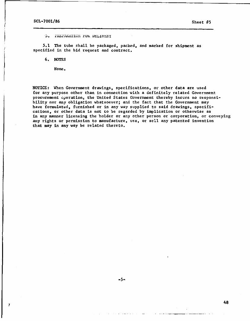
SCL-7001/86 Sheet #5
5.1 The tube shall be packaged, packed, and marked for shipment asspecified in the bid request and contract.
6. NOTES
None.
NOTICE: When Government drawings, specifications, or other data are usedfor any purpose other than in connection with a definitely related Governmetitprocurement oderation, the United States Government thereby incurs no responsi-bility nor any obligation whatsoever; and the fact that the Government mayhave formulated, furnished or in any way supplied to said drawings, specifi-cations, or other data is not to be regarded by implication or otherwise asin any manner licensing the holder or any other person or corporation, or conveyingany rights or permission to manufacture, use, or sell any patented inventionthat may in any way be related thereto.
"-5-
48
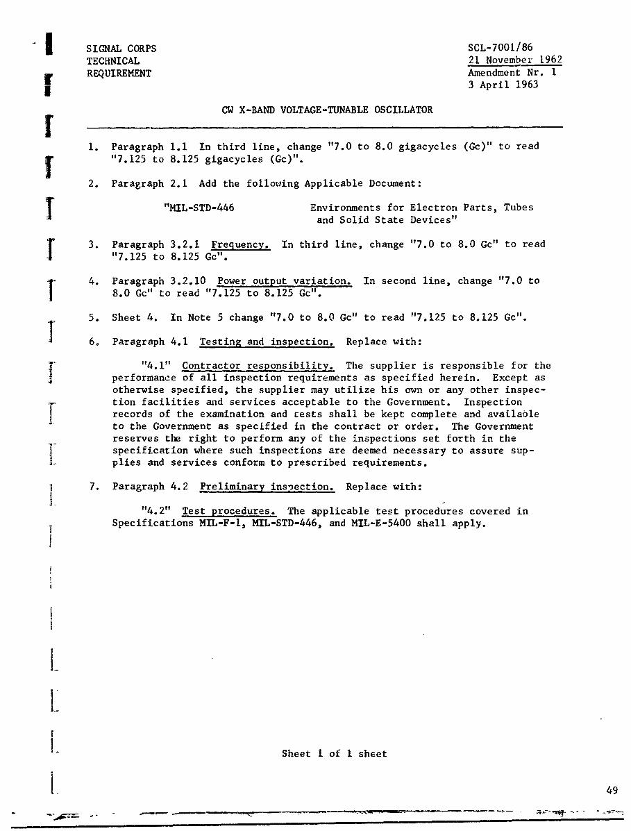
I SIGNAL CORPS SCL-7001/86TECHNICAL 21 November 1962
REQUIREMENT Amendment Nr. 13 April 1963
CW X-BAND VOLTAGE-TUNABLE OSCILLATOR
1. Paragraph 1.1 In third line, change "7.0 to 8.0 gigacycles (Gc)" to read"7.125 to 8.125 gigacycles (Gc)".
2. Paragraph 2.1 Add the following Applicable Document:
"MIL-STD-446 Environments for Electron Parts, Tubesand Solid State Devices"
S3. Paragraph 3.2.1 Frequency. In third line, change "7.0 to 8.0 Gc" to read"7.125 to 8.125 Gc".
4. Paragraph 3.2.10 Power output variation. In second line, change "7.0 to8.0 Gc" to read "7.125 to 8.125 Gc".
5. Sheet 4. In Note 5 change "7.0 to 8.0 Gc" to read "7.125 to 8.125 Gc".
1 6. Paragraph 4.1 Testing and inspection. Replace with:
"4.1" Contractor responsibility. The supplier is responsible for theperformance of all inspection requirements as specified herein. Except asotherwise specified, the supplier may utilize his own or any other inspec-tion facilities and services acceptable to the Government. Inspection
-I records of the examination and rests shall be kept complete and availableto the Government as specified in the contract or order. The Governmentreserves the right to perform any of the inspections set forth in thespecification where such inspections are deemed necessary to assure sup-plies and services conform to prescribed requirements.
1 7. Paragraph 4.2 Preliminary ins-ection. Replace with:
"4.2" Test procedures. The applicable test procedures covered inSpecifications MIL-F-I, MIL-STD-446, and MIL-E-5400 shall apply.
I-
Sheet 1 of I sheet
1 49
APPENDIX II TECHNOLOGY OF TUBE FABRICATION
The assembly and material practices used in the fabrication of the vacuum
urits are the best known procedures for insuring ultra clean and ultra-high
vacuum devices. All metallic components are chemically and ultrasonically cleaned
and vacuum fired before assembly begins. (Cleaning procedures may be obtained
from Rosebury's "Handbook of Electron Tube and Vacuum Techniques" Addison-Wesley
Publishing Company.) All ceramics without metallizing are air fired and metallized
ceramics are ultrasonically cleaned in a solvent or hydrogen fired. Clean room
procedures are observed strictly during the assembly and brazing of the units.
The first sub-assembly is the filament unit. A filament, ceramic, and buttons
are assembled and brazed with an alignment jig at a temperature higher than
subsequent brazes will occur. The actual temperature will depend on the brazing
material which is used. A variety of alloys are available which are suitable for
this assembly. After the unit has been brazed, the filament is flashed in an
atmosphere of Benzene. This procedure isstandard practice for carbonizing the
emitter. (A discussion of this procedure is given in Kohls "Materials and
Techniques for Electron Tubes" Reinhold Publishing Corporation.)
The filament sub-assembly is then combined with the remaining tube components
(with the exception of the cold cathode) on a precision alignment jig. Brazing
material is inserted at each metal to ceramic junction and pressure is applied to
the assembly during brazing.
The body sub-assembly is then removed from the alignment jig and the cold
cathode is then brazed at a lower temperature. The tube is checked for vacuum
tightness and conducting film then aged for a periodof twenty four hours.
50
49
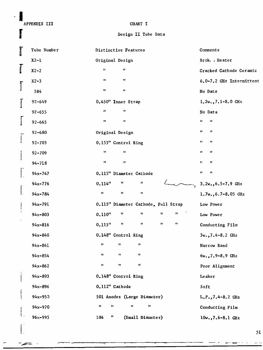
APEDI I Design IITube Data
Tube Number Ditntv etrsComments
X2-1 Original Design Brok,, Heater
T X2-2 ""Cracked Cathode Ceramic
x2 -3 "6.0-7.2 0Hz Intermittent
584 No Data
f 92-649 0.450" Inner Strap 1.2w.,7.1-8.0 GHz
92-655it itNo Data
92-665 It it It of
92-680 Original Design it o
92-703 0.153" Control Ringit f
j 92-709 "I I f
94-718 II t
94x-747 0.115" Diameter Cathode" "
94x-776 0. 114" it - 3.2w.,6.5-7.9 GHz
* 94x-784 1 .7w.,6.7-8.05 GHz
94x-791 0.115" Diameter Cathode, Full Strap Low Power
943c-803 0.110", it"" Low Power
94x-816 0.115", "1 of" Conducting Film
94x-840 0.148" Control Ring 3w.,7.4-8.2 0Hz
94x-841 to of Narrow Band
94x-854 it it 6w..,7.9-8.9 0Hz
94x-862 " "Poor Alignment
94x-893 0.148" Control Ring Leaker
94x-896 0.112" Cathode Soft
94x-953) 501 Anodes (Large Diameter) L.P.,7.4-8.2 0Hz
94 x-970 " '" "Conducting Film
96x-995 584 " (Small Diameter) lOw.,7.6-8.l 0Hz
51
Tube Number Distinctive Features Comments
96x-999 584 Anodes (Small Diameter) Leaker
96x-1012 0.110" Cathode Broken Heater
96x-1013 o " Low Power
96x-1021 0.115" " No Data
96x-1034 No Data Conducting Film
96 -1043 " " Conducting Film
96 -1045 " " it
96x-1057 501 Anodes (Large Diameter) Poor Alignment
96x-1059 Straightened vanes 4w., 6.8-8.1 GHz
96-1071 No Data Poor Performance
96x-1085 0.065 Filament Ceramic Shorted Strap
96x-1086 501 Anodes (Large Diameter) Narrow Band
96x-1087 " " Misaligned
96x-1097 0.055" Filament Narrow Band
96x-1102 Copper Internal Strap No Data
96x-1106 No Straps Multiple Modes
96x-1158 No Data Leaker
96x-1176 501 Anodes Copper Strap (Large Diam) 10w., 6.9-7.9 Qz
96x-1185 0.075" Filament Good Performance
96x-1200 584 Anodes (Small Diameter) Low Frequency
96x-1211 " 0.110" Diameter Cathode Poor Performance
96x-1217 No Data No Data
96x-1221 501 Anode (Large Diameter) " "
96x-1228 " " " " " "
52
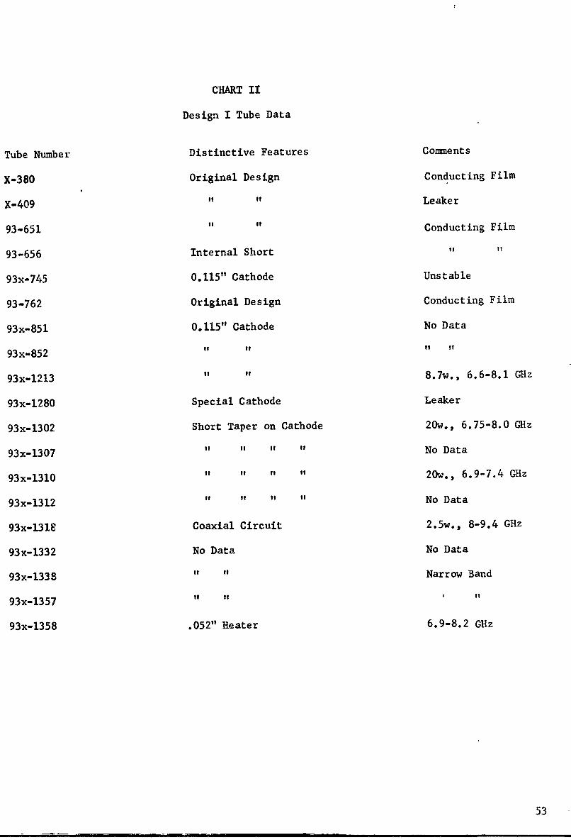
CHART II
Design I Tube Data
Tube Number Distinctive Features Coments
X-380 Original Design Conducting Film
X-409 " " Leaker
93-651 Conducting Film
93-656 Internal Short " "
93x-745 0.115" Cathode Unstable
93-762 Original Design Conducting Film
93x-851 0.115" Cathode No Data
93x-852 if " " "
93x-1213 " " 8.7w., 6.6-8.1 GHz
93x-128 0 Special Cathode Leaker
93x-130 2 Short Taper on Cathode 20w., 6.75-8.0 GHz
93x-13 0 7 " " " " No Data
93x-1310 I " " " 20w., 6.9-7.4 GHz
93x-1312 " " " if No Data
93x-1318 Coaxial Circuit 2.5w., 8-9.4 GHz
93x-133 2 No Data No Data
93x-1338 " " Narrow Band
93x-1357 " " 4 "
93x-1358 .052" Heater 6.9-8.2 GHz
53
CHART III
Modified Design I (Short) Tube Data
Tube Number Distinctive Features Comnents
98-1361 Filed Down (Design ])Anodes Gassy
98-1369 " f it "
98-1372 "" of " i
98-1423 it" " " Narrow
98-1424 , !t No Data
98-1431 " I " " 12w., 7.2-8.1 GHz
98-1462 " "it Gassy
98-1463 Short Tube Parts Narrow Band
-98-1570 Staggered Vanes Leaker
98-1571 I" No Data
98-1577 No Data " "
98-1578 " " Narrow Band
98-1589 0.160" Diameter Control Ring " "
98x-1590 f t " I
98x-1599 " it it
98-1600 Vanes Staggered " "
98-1601 No Data it
98-1612 Flat Cathode No Data
98-1613 " i Leaker
98x-1659 No Data No Data
98x-1660 Tapered Cathode Excellent
98x-1672 ,, it Leaker
98x-1725 Flat Cathode No Data
98x-1752 0.153" Control Ring " "
98x-1760 " " ",
54
Tube Number Distinctive Features Comments
-8x-1761 0.153" Control Ring No Data
98x-1762 Tapered K. 0.153" C.R. " "
1> 98x-1763 Flat Cathode , Low Power
98x-1765 " " Poor
i 98x-1769 Tube .010" Shorter Narrow Band
[ 98x-1770 " " t
98x-1775 Flat Cathode Gassy
F 98x-1776 Flat Cathode 0.160" C.R. 9wpk, 6.75-8.55 GHz
98x-1777 Tapered Cathode " No Data
F 98x-1782 Flat Cathode " U "
F 98x-1783 " " " Narrow Band
98x-1844 " " " No Data
- 98x-1868 " " " Low Power Good C.R. Range
98x-1893 Tapered Cathode 0.153" C.R., .0085" Heater Narrow Band 6000 C.R.
F- 98x-1894 Flat Cathode " " No Data
1-L
S55
CHART IV
Miscellaneous Tube Data
Tube Number Distinctive Features Comments
8-594 8 Vane Design I No Data
82-721 it it a of
82x-724 "t If i "
82x-725 " i
82-732 .070'"indow (0-mode) I t
7-730 Reg. 7 Vane Anodes i t
93x-742 7 Vane Design i 4-6GHz TNC
93x-757 8 Vane Design I No Data
93x-758 " " it
93x-782 It" 0.115"Cathode 0-mode 8w., 7.0-8.0 GHz
93x-783 i " 7.5w., 7.0-8.0GHz
93x-802 " I Film
93x-801 " i No Data
93x-85# it o 0.115 Diameter Cathode " "
82x-919 Internal Shorts (0-mode) - it
83x-MRB 8 Vane Design I " if
93x-1170 P " I "
83x-1212 of" "
83x-1241 i o Shorted
83x-1256 " o Leaker
66-1540 6 Vane Diesign I No Data
66-1541 It is It 31
100-1620 20 V., .075"Diam Cath, Htr 0.140"Anode No Start
100-1637 is it o f
100-1638 " " o Shorted Heater
56
!
S Tube Number Distinctive Peaturpt Cement
% 100-1639 20 V., .075"Diam Cath, Htr 0.140"Anode N.B. 9.4 GHz
99-1644 18 Vanes No Start
99-1645 it "1 o f
!. 99-1888 " "
£r
Iz
[
L
L
LI ,
- 57
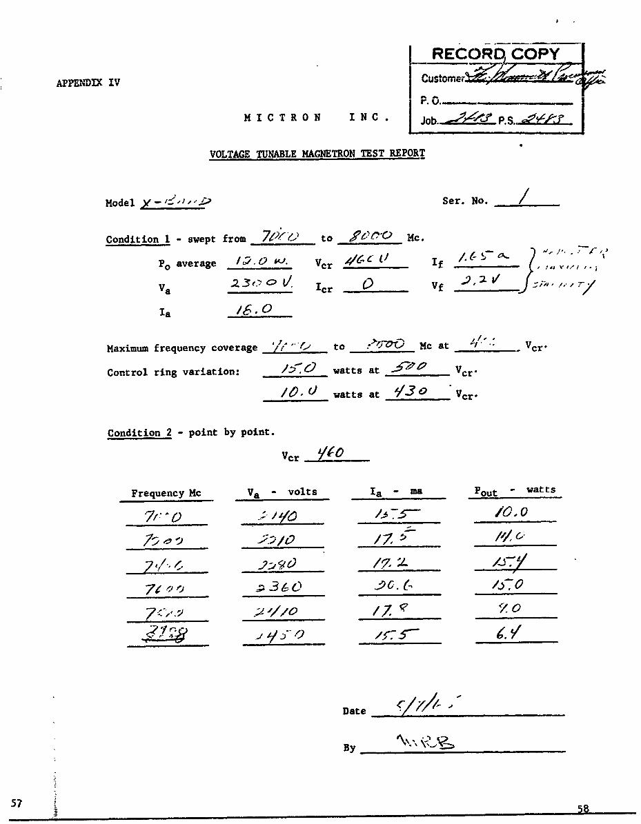
RECRD COPY
APPENDIX IV Custome,
M. 0-C.,.M I C T R 0 N I N C Jo___,.,ps .• -
VOLTAGE TUNABLE MAGNETRON TEST REPORT
Model y-'J-'-" Ser. No. /
Condition 1 - swept from 7______ to M___-__ 14c.
ma /6.0
Maximum frequency coverage '/{ .. "- to •>0O Mc at " - Vcr.
Control ring variation: /_ watts at __P_70 _ Vcr.
/_ _ d watts at /13 0 Vcr.
Condition 2 - point by point.
Vcr __ _
Frequency Mc Va - volts Ia - ma Pout - watts
7,''0 . J,/•/-4 . /0,o
, c4) /. L0
__"__._ •-//o ,,______ ___.__
Date .
By
57
V 58F
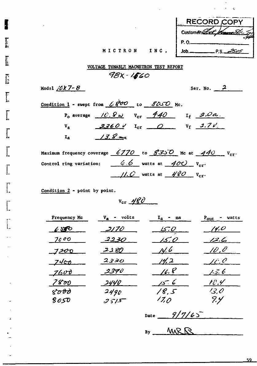
RECORD COPY
SP. nM IMICTRON I N C , Job. P.S. - J A -•___
VOLTAGE TUNABL1 MAGNETRON TEST REPORT
Model L06 7- 8 Ser. No. _ 2
r
Condition 1 - swept from 0 0 to ___-__ ) Mc.
f Po average le, -9 &) Vcr l 0 If ,
Va mU6 40 &/ Icr V Vf ,. 7 4.[Ia /'?, S90•
I Maximum frequency coverage 6-77ZO to e_7,5-0 Mc at .40 Vcr.
Conitrol ring variation: •f. .67 watts at 4 Vcr.
0 watts at • Vcr.
Condition 2 - point by point.
Vcr "ec
Frequency Mc Va - volts Ia - ma Pout " watts
7C 0-0 4__r-__ OLL
~~~;:- ._,5,-- 17- 9 O ./,/,v•
7,/', 2 .. y /•,* 2 .
Date __ _ _ _ _ _ _ _ _ _
By , S..
-- 5
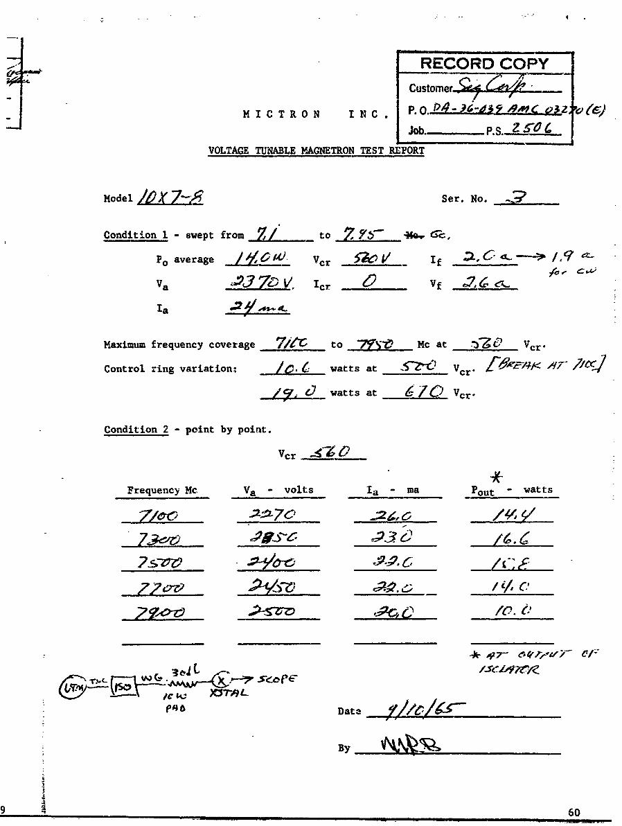
RECORD COPY
Customer $, Qe Cc
j MICTRON INC. N C P. 0.jJob..
VOLTAGE TUNABLE MAGNETRON TEST RE-PORT
Model Ser. No. _
Condition 1 - swept from to Y(a., Cc,
PO average Vcr SZ V - If .C& /Va 22 ZQ V. •c, ____ Vf Zc, a.
Ia
Maximum frequency coverage 71/C to 7 Mc at -'b" 94 Vcr.
Control ring variation:- watts at - Vcr*. ,7 1
watts at 7C- Vcr.
Condition 2 - point by point.
Vcr -
Frequency Mc Va - volts Ia - ma Pout - watts
,770-0~ ~ ~lo 5d/le-le,-c..,.,/ ,c
p#4 •Datý-
9 - 6 0
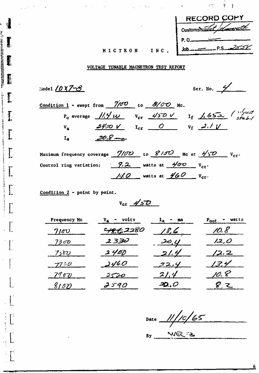
CustomP5 [ P. 0... .... . .
t VOLTAGE TUNABLE MAGNETRON TEST REPORT
-iodel 8 Ser. No.•rCondition 1 - swept from 7*v to __610 _ Mc.
P. average A/1 W Vcr 4/5 D " If Z 6 5-,.
Va _._ _-_0 V ' cr ... _0 Vf _._I __
f Maximum frequency coverage 7/t5 to M/___ Mc at Vcr.
Control ring variation: - . watts at .Va-' Vcr*
watts at Vcr.
L: Condition 2 - point by point.
Vcr _____
Frequency Mc Va - volts la - ma Pout - watts
Fi
I-
1_ faq o .. __ o__..
Date /_ _ _'"
By -
[ l o_. _-76

RECORD!ROPY
P.0. - o.. .
M I C T R 0 N I N C . Job-. P.S.Jcb
VOLTAGE TUNABLE MAGNETRON TEST REPORT
Model Ser. No.
Condition 1 - swept from to e-0 Mc.
PO average 6 Vcr ,.o I'f Z
Va S- 6 V Cr .~ Vj
la.
Maximum frequency coverage to Mc at Vcr.
Control ring variation: watts at. Vcr
watts at Vcr.
Condition 2 - point by point.
Vcr
Frequency Mc Va - volts Ia - ma Pout " watts
,or, 0ý- 9W
Date 44
By _ _ _ _ _ _ _ _ _ _ _ _
62
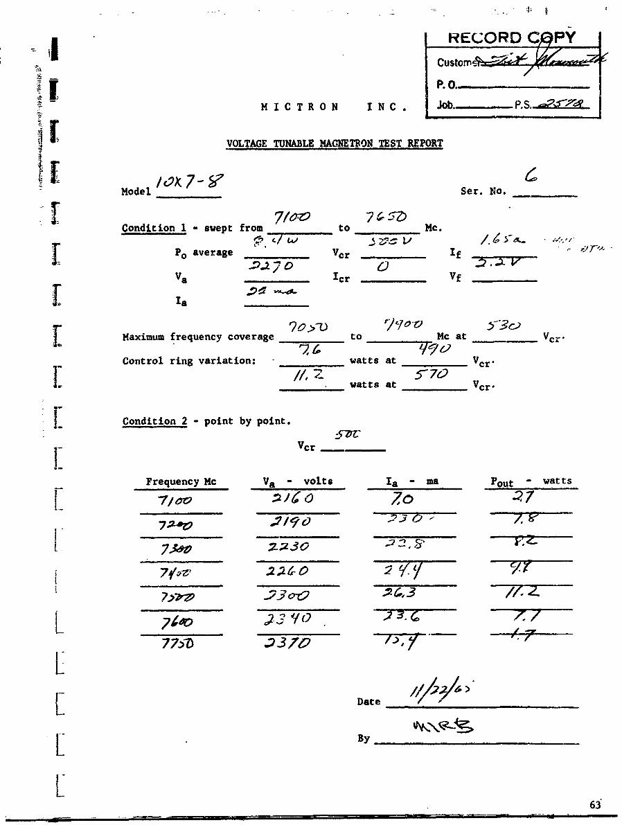
RECORD q9 PY
M ICT RO0N IN C Jo.- P.S
VOLTAGE TUNABLE MACNETRON TEST REPORT
Model lox_7-_VSer. No.
Condition 1 - swept from to "I 5_. _, Mc.
I: PO average Vcr If "Va Icr Vf
Maximum frequency coverage to Mc at Vcr.
Control ring variation: watts at Vcr.
. watts at Vcr.
L• Condition 2 - point by point.
Vcr _____
Frequency Mc Va - volts Ia -ma Pout - wattsL- 7,ov;• 70 " ,~0 ... ... o9 -?, 7
I - _ __,, i_
770t :?3710
Date _ _ _ _ _ _ _ _ _ _ _ _ _ _ _
LBy
63
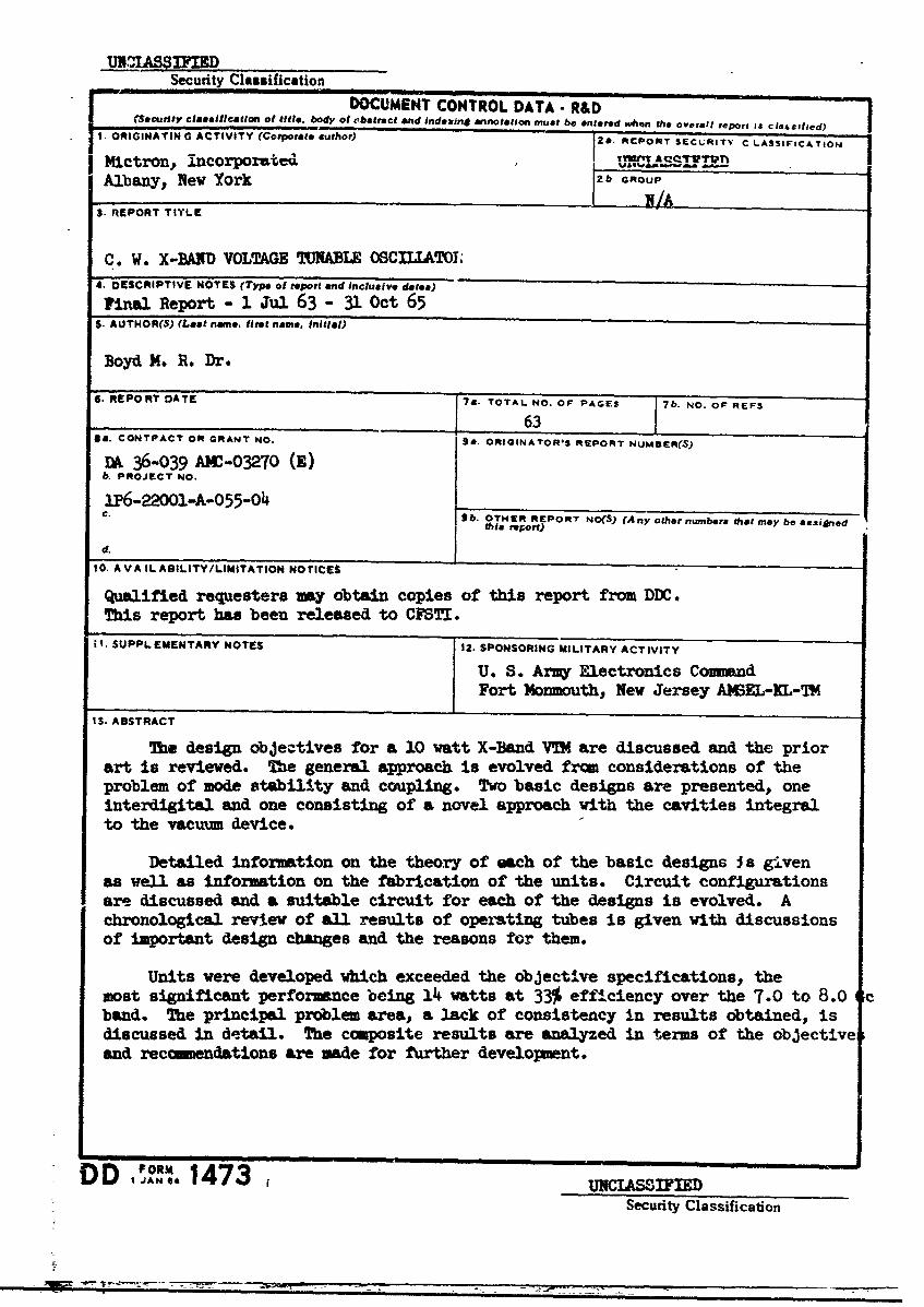
umIAS$IFIEDSecurity Classification
DOCUMENT CONTROL DATA - R&DSecurtty claselficetion of title, body of rbatract *rad indexing annotation muet be entered viAn the ovterall repor ias cIla&sted)
I. ORIGINATING ACTIVITY (Corporate author) 2a. REPORT SECURITY CLASSIFICATION
i 1WP? ACQTVTIlMictron, incorporated, .AAlbany, New York 2zb aoup
3. REPORT TITLE
C. W. X-BAND VOLTAGE JITNABLE OSCILIATOL
4. DESCRIPTIVE NOTES (Type of report end inclusive datea)
Final Report - 1 Jul 63 - 31 Oct 65S. AUTHOR(S) (Loat amie. first name, Initial)
Boyd 1. R. Dr.
6. REPORT DATE )7a. TOTAL NO. OF PAGES 7b. NO. OF REFS
_ 63II. CONTPACT OR GRANT NO. 9&. ORIGINATOR'S REPORT NUMBER(S)
DA 36-039 AMI-03270 (E)b. PROJECT NO.
IP6-22001-A-055-o04C. 9b. OTHER REPORT NO(S) (Any other numberm that may be assigned
this report)
d.
10. A V A IL ABILITY/LIMITATION NOTICES
Qualified requesters my obtain copies of this report from DDC.This report has been released to CFSTI.
i1. SUPPLEMENTARY NOTES 12. SPONSORING MILITARY ACTIVITY
U. S. Arny Electronics CommandFort Momuouth, New Jersey ANSEL-KL-TM
13 ABSTRACT
7he design objectives for a 10 watt X-Band VTi are discussed and the priorart is reviewed. The general approach is evolved from considerations of theproblem of mode stability and coupling. Two basic designs are presented, oneinterdigital and one consisting of a novel approach with the cavities integralto the vacuum device.
Detailed information on the theory of each of the basic designs J s givenas well as information on the fabrication of the units. Circuit configurationsare discussed and a suitable circuit for each of the designs is evolved. Achronological review of all results of operating tubes is given with discussionsof important design changes and the reasons for them.
Units were developed which exceeded the objective specifications, themost significant performance being 14 watts at 33% efticiency over the 7.0 to 8.0 cband. The principal problem area, a lack of consistency in results obtained, isdiscussed in detail. The composite results are analyzed in terms of the objectiveand recmendations are made for further developuent.
DD IoJAN$ 1473 CU S•curityClaCiAfcIFatio= Security Classification
Security Classificationj14, LINK A LINK B LINK C
KEY WORDS -..
r ROLE * ROLE~ WT RL WI
Electron TubesMicrowave Oscillators3ManetronsVoltage Twmble Magiietrons
INSTRUJCTIONS
I. ORIGINATING ACTIVITY: Enter the name and address 10. AVAILABILITY/LIMITATION NOTICES: Enter any lir-of the contractor, subcontractor, grantee, Department of De- itations on further dissemination of the report, other than thosefense activity or other organization (corporate author) issuing iposed by security classification, using standard statementsthe report, such as:
2a. REPORT SECUM4TY CLASSIFICATION: Enter the over- (1) "Qualified requesters may obtain copies of thisall security classification of the report. Indicate whether report from DD ""Restricted Data" Is included. Marking is to be in accord-ance with appropriate security regulations. (2) "Foreign announcement and dissemination of this
2b. GROUP: Automatic downgrading is specified in DoD Di- report by DDC is not authorized."rective 5200. 10 and Armed Forces Industrial Manual. Enter (3) "U. S. Government agencies may obtain copies ofthe group number. Also, when applicable, show that optional this report directly from DDC. Other qualified DDCmarkings have been used for Group 3 and Group 4 as author- use-s shall request throughized.
3. REPORT TITLE: Enter the complete report title in all (4) "U. S. military agencies may obtain copies of thiscapital letters. Titles in all cases should be unclassified. report directly from DDC Other qualified usersIf a meaningful title cannot be selected without classifica-. shall request throughtion, show title classification in all capitals in parenthesisImmediately following the title. •_,_
4. DESCRIPTIVE NOTES: If appropriate, enter the type of (5) "All distribution of this report is controlled. Qual-report, e.g., interinm, progress, summary, annual, or final. ified DDC users shall request throughGive the inclusive dates when a specific reporting period iscovered. -
If the report has been furnished to the Office of Technical5r AUThpOR(St Enter the name(s) of author(s) as shown on Services, Department of Commerce, for sale to the public, indi-or in thi report. Enter lost name, first name. middle initial. cate this fact and enter the price, if known.If military, show rank and branch of service. The name ofthe principal author is an absolute mir'mum requirement. IL SUPPLEMENTARY NOTES. Use for additional explana-
6. REPORT DATE: Enter the date of the report as day, tory notes. I
month, year; or month, year. If more than one date appears 12. SPONSORING MILITARY ACTIVITY: Enter the name ofon the report, use date of publication. the departmental project office or laboratory sponsoring (payr
gin for) the research and development. Include address.7 a. TOTAL NUMBER OF PAGES: The total page countshould follow normal pagination procedures, Le., enter the 13. ABSTRACT: Enter an abstract giving a brief and factualnumber of pages containing information, summary of the document indicative of the report, even though
it may also appear elsewhere in the body of the technical re-7b. NUMBER OF REFERENCES: Enter the total number of port. If additional space is required, a continuation sheetreferences cited in the report. shall be attached.
8a. CONTRACT OR GRANT NUMBER_ If appropriate, enter It is highly desirable that the abstract of classified re-the applicable number of the contract or grant under which ports be unclassified. Each paragraph of the abstract shallthe report was written. end with an indication of the military security classification
8b,.8c, & 8d. .PROJECT NUMBER: Enter the appropriate of the information in the paragraph, represented as (TS), (S),military department identification, such as project ra.mber, (C), or (U).subproject number, system numbers, task number, etc: There is no limitation on the length of the abstract. How-
9a. ORIGINATOR'S REPORIT NUMBER(S): Enter the offi- ever, the suggested length is from 150 to 225 words.cial report number by which the document will be identified 14. KEY WORDS: Key words are technically meaningful termsand controlled by the originating activity. This number must or short phrases that characterize a report and may be used asbe unique to this report, index entries for cataloging the report. Key words must be
9b. OTHER REPO'.AT NUMBER(S): If the report has been selected so that no security classification is required. Iden-
assigned any other report numbers (either by the originator fiers, such as equipment model designation, trade name, -till-
or by the sponsor), also enter this number(s). tary project code name, geographic location, may be used askey words but will be followed bv an indication of technicalcontext. The assignment of links, rules, and weights isoptional.
UNCLSSFIDSecurity Classification •
- . - - ~- - ---