Embed Size (px)
Citation preview

©2018TechSearch International,Inc.
TechSearch International, Inc.Corporate Overview
E. Jan Vardaman, President

©2018TechSearch International,Inc.
Corporate Background
• Founded in 1987 and headquartered in Austin, Texas
• Recognized around the world as a leading consulting company in the field of advanced packaging technology
• Specialists in advanced semiconductor packaging and assembly, electronics manufacturing, and materials
• What sets TechSearch International apart from others?üWe have close relationships with companies and industry leaders built on trust
and mutual respect
üWe ask customers what they want—report content is constantly tailored to meet those needs
üWe provide complete, concise, accurate data, and unbiased opinions
üWe participate in many industry conferences to share our findings and stay up-to-date on the latest innovations
üWe frequently tour PCB, EMS, and OSAT manufacturing facilities
YEARS OF TECHSEARCH INFLUENCE1987 Now

©2018TechSearch International,Inc.
How can we help you?...Our Mission
• Enable clients to capitalize on opportunities for profitable growth with our Accurate è Relevant è Timely è Market and technology analysis
• Provide tools that enable success:üAuthentic technical and economic analysis of market and technology
trends in semiconductor packaging, assembly, and materialsüFrequent updates on the latest technology developmentsüStrategic planning and execution assistanceüTechnology licensing and connecting partners for joint developmentüCost analysis with software models
• Participate directly with client teams in providing an understanding of changes and drivers in the marketplace
• Provide competitive analysis of semiconductor packages, materials, and assembly equipment marketplaces to aid new product introductions

©2018TechSearch International,Inc.
Market analysis you can trust!...Multi-client reports
• Flip Chip and WLP Market and Technology Analysis
• New Frontiers in Automotive Electronic Packaging
• SiP for Mobile and Wearable Applications
• Global Semiconductor Packaging Materials OutlookPARTNERSHIP WITH SEMI
• Worldwide OSAT Manufacturing Sites DatabasePARTNERSHIP WITH SEMI
• 3D IC Gap Analysis: Remaining Issues, Solutions, Market Status
• Advanced Packaging Cost Models and AnalysisPARTNERSHIP WITH SAVANSYS
• Advanced Packaging Update (4 issues each year)
– Economic and business developments in the semiconductor packaging and assembly industry including market forecast by package type (FBGA, FLGA, QFN, stacked die CSP, PoP, etc.)
– New packages and materials including trends and drivers
– Various market and technology analysis
©2018TechSearch International,Inc.
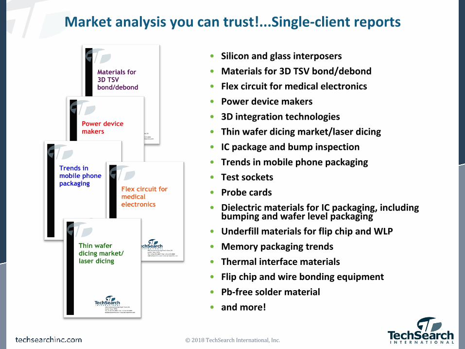
Market analysis you can trust!...Single-client reports
• Silicon and glass interposers• Materials for 3D TSV bond/debond• Flex circuit for medical electronics• Power device makers• 3D integration technologies• Thin wafer dicing market/laser dicing• IC package and bump inspection• Trends in mobile phone packaging• Test sockets• Probe cards• Dielectric materials for IC packaging, including
bumping and wafer level packaging• Underfill materials for flip chip and WLP• Memory packaging trends• Thermal interface materials• Flip chip and wire bonding equipment• Pb-free solder material• and more!

©2018TechSearch International,Inc.
At the forefront…Recognizing emerging trends
• Automotive Electronics
First industry analysis of packages for automotive electronics with a focus on ADAS
• Flip Chip Trends
Publishing reports on flip chip markets and technology trends since 1994 — We’ve done cutting edge analysis in recognition of the shift to Cu pillar
• WLP Demand and Capacity
Tracking wafer bump and WLP capacity and demand trends since 2003 — We've been at the front in recognizing the shift to fan-out WLP (FO-WLP)
• Ball Grid Arrays and Chip Size Packages
First industry analysis of the ball grid array market in 1994 — We’ve published annual forecasts of BGA and CSP demand ever since
• 3D IC with TSVs and Si Interposers
We are recognized as the provider of realistic market forecasts — We are unique in offering gap analysis, with indications of key areas requiring additional work
• System-in-Package and Multichip Modules
Tracking markets and trends since 1990
SiP Market by Device Type
Copper Pillar Demand on 300mm Wafers
Fan-In WLP Demand in 200mm Equiv. Wafers
0
2,000
4,000
6,000
8,000
10,000
12,000
14,000
16,000
18,000
20,000
2015 2016 2017 2018 2019 2020
Thou
sand
s of 2
00m
m E
quiv
alen
t Waf
ers
Other Image Sensor RF Analog/Mix-Sig
© 2017 TechSearch International, Inc.
0
4,000
8,000
12,000
16,000
2015 2016 2017 2018 2019
Thou
sand
s of 3
00m
m W
afer
s
Cu Pillar on 300mm Wafer DemandCu Pillar on 300mm Wafer Capacity Planned
© 2017 TechSearch International, Inc.
RF Modules
Connectivity Modules
APs, Modems & Hardware Platform Modules
MEMS Inertial Sensors, Hubs & Nodes
Stacked-CIS Camera Modules
Other Mobile, Wearable & Consumer
PMUs, Voltage Regulators & High Power Modules
Silicon Interposers & 3D TSV DRAMs
Automotive Sensors & Modules
Mobile, Wearable & Consumer Devices
© 2016 TechSearch International, Inc.

©2018TechSearch International,Inc.
Technology Licensing Examples
• NTT’s copper polyimide thin film technology from Japan to the United States
• Matsushita’s TBTAB technology
• Aptos gold bump technology from the United States to Taiwan
• Tessera’s µBGA technology from the United States to Korea
• Flip chip assembly and solder bumping technology
• 3D Plus stacking technology
• Beltronics inspection technology from the United States to Japan

©2018TechSearch International,Inc.
Cost Analysis Software Models
Wire Bond, Flip Chip, and Wafer Level Package Models• Wire bond cost analysis
– Copper versus gold wire trade-offs
• Flip chip cost analysis
• WLP and FO-WLP cost analysis
• Collaboration with SavanSys Solutions
– SavanSys develops model software– TechSearch helps with model calibration
2.5D and 3D Packaging Cost Model• After successful collaboration on cost models for other packaging technologies,
SavanSys and TechSearch introduced a cost model for 2.5D and 3D packaging
• The first cost model to cover the total cost and yield from fabrication of the wafer to complete assembly, for both 2.5D and 3D
• Detailed manipulation of the process flow to meet user requirements is possible
©2018TechSearch International,Inc.
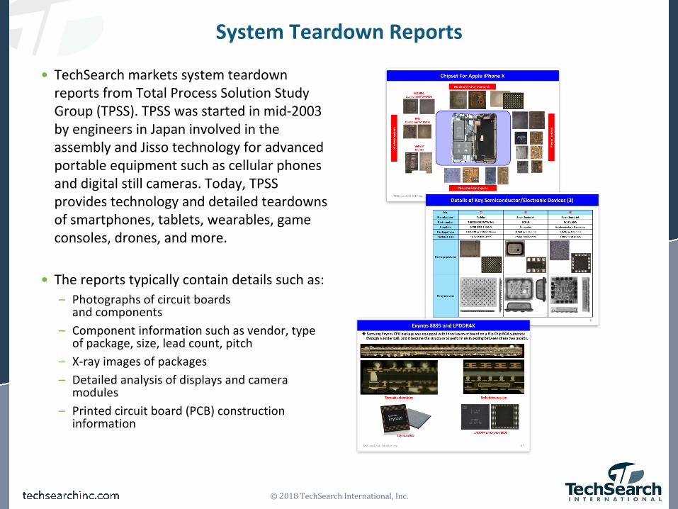
System Teardown Reports
• TechSearch markets system teardown
reports from Total Process Solution Study
Group (TPSS). TPSS was started in mid-2003
by engineers in Japan involved in the
assembly and Jisso technology for advanced
portable equipment such as cellular phones
and digital still cameras. Today, TPSS
provides technology and detailed teardowns
of smartphones, tablets, wearables, game
consoles, drones, and more.
• The reports typically contain details such as:
– Photographs of circuit boards and components
– Component information such as vendor, type of package, size, lead count, pitch
– X-ray images of packages
– Detailed analysis of displays and camera modules
– Printed circuit board (PCB) construction information

©2018TechSearch International,Inc.
Workshops, Conference Presentations, and Exhibitions
• Workshops on relevant topics such as wearables, medical electronics, flip chip, 3D TSV, embedded components, optoelectronics, automotive electronics, and substrates
– Periodic topical workshops in Austin, Texas– Together with the Fraunhofer Institute, we host a workshop in Munich, Germany,
the day before Productronica
• Recent Conference Presentations and Exhibitions– ADAS Sensors Conference and Exhibition – Detroit, Michigan
– IMAPS International Conference on Device Packaging – Fountain Hills, Arizona
– International Wafer Level Packaging (IWLPC) – San Jose, California
– IEEE Electronics Components and Technology (ECTC) – San Diego, California
– NEPCON Japan, IC & Sensor Packaging Technology Expo – Tokyo, Japan
– Fraunhofer IZM Panel Level Packaging Symposium – Berlin, Germany
– IEEE CPMT Symposium – Kyoto, Japan
– IMAPS International Symposium on Microelectronics – Raleigh, North Carolina
– SEMICON China – Shanghai, China
– Design Automation Conference (DAC) – Austin, Texas
– The ConFab – San Diego, California

TechSearch International, Inc.4801 Spicewood Springs Road, Suite 150
Austin, Texas 78759 USA+1.512.372.8887
Thank you!
TechSearch International, Inc.4801 Spicewood Springs Road, Suite 150
Austin, Texas 78759 USA+1.512.372.8887
Thank you!
©2018TechSearch International,Inc.