Embed Size (px)
Citation preview
Technology
Technology and SystemHardware OverviewTechnologyPulsedLight's "Time-of-flight "distance measurement technology is based on the precise
measurement of the time delay between the transmission of an optical signal and its
reception. Our patented, high accuracy measurement technique enables distance
measurement resolution down to 1cm by the digitization and averaging of two signals; a
reference signal fed from the transmitter prior to the distance measurement and a received
signal reflected from the target. The time delay between these two stored signals is
estimated through a signal processing approach known as correlation, which effectively
provides a signature match between these two closely related signals. Our correlation
algorithm accurately calculates the time delay, which is translated into distance based on the
known speed-of-light. A benefit of PulsedLight's approach is the efficient averaging of low-
level signals enabling the use of relatively low power optical sources, such as LEDs or VCSEL
(Vertical-Cavity Surface-Emitting) lasers, for shorter-range applications and increased range
capability when using high power optical sources such as pulsed laser diodes.
System HardwareThe Single Board Sensor provides distance and velocity measurements in an ultra-small form
factor. This small size is the result of PulsedLight's System-On-Chip (SoC) signal processing
technology which, beyond being small, reduces the complexity and power consumption of
supporting circuitry. The system consists of three key functionalities:
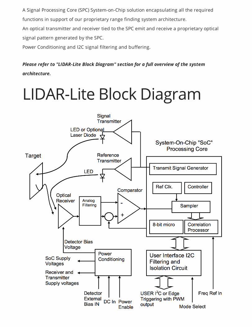
A Signal Processing Core (SPC) System-on-Chip solution encapsulating all the required
functions in support of our proprietary range finding system architecture.
An optical transmitter and receiver tied to the SPC emit and receive a proprietary optical
signal pattern generated by the SPC.
Power Conditioning and I2C signal filtering and buffering.
Please refer to "LIDAR-Lite Block Diagram" section for a full overview of the system
architecture.
LIDAR-Lite Block Diagram
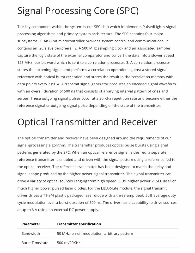
Signal Processing Core (SPC)The key component within the system is our SPC chip which implements PulsedLight's signal
processing algorithms and primary system architecture. The SPC contains four major
subsystems; 1. An 8-bit microcontroller provides system control and communications. It
contains an I2C slave peripheral. 2. A 500 MHz sampling clock and an associated sampler
capture the logic state of the external comparator and convert the data into a slower speed
125 MHz four bit word which is sent to a correlation processor. 3. A correlation processor
stores the incoming signal and performs a correlation operation against a stored signal
reference with optical burst reception and stores the result in the correlation memory with
data points every 2 ns. 4. A transmit signal generator produces an encoded signal waveform
with an overall duration of 500 ns that consists of a varying interval pattern of ones and
zeroes. These outgoing signal pulses occur at a 20 KHz repetition rate and become either the
reference signal or outgoing signal pulse depending on the state of the transmitter.
Optical Transmitter and ReceiverThe optical transmitter and receiver have been designed around the requirements of our
signal-processing algorithm. The transmitter produces optical pulse bursts using signal
patterns generated by the SPC. When an optical reference signal is desired, a separate
reference transmitter is enabled and driven with the signal pattern using a reference fed to
the optical receiver. The reference transmitter has been designed to match the delay and
signal shape produced by the higher power signal transmitter. The signal transmitter can
drive a variety of optical sources ranging from high speed LEDs, higher power VCSEL laser or
much higher power pulsed laser diodes. For the LIDAR-Lite module, the signal transmit
driver drives a T1-3/4 plastic packaged laser diode with a three-amp peak, 50% average duty
cycle modulation over a burst duration of 500 ns. The driver has a capability to drive sources
at up to 6 A using an external DC power supply.
Parameter Transmitter specification
Bandwidth 50 MHz, on-off modulation, arbitrary pattern
Burst Time/rate 500 ns/20KHz
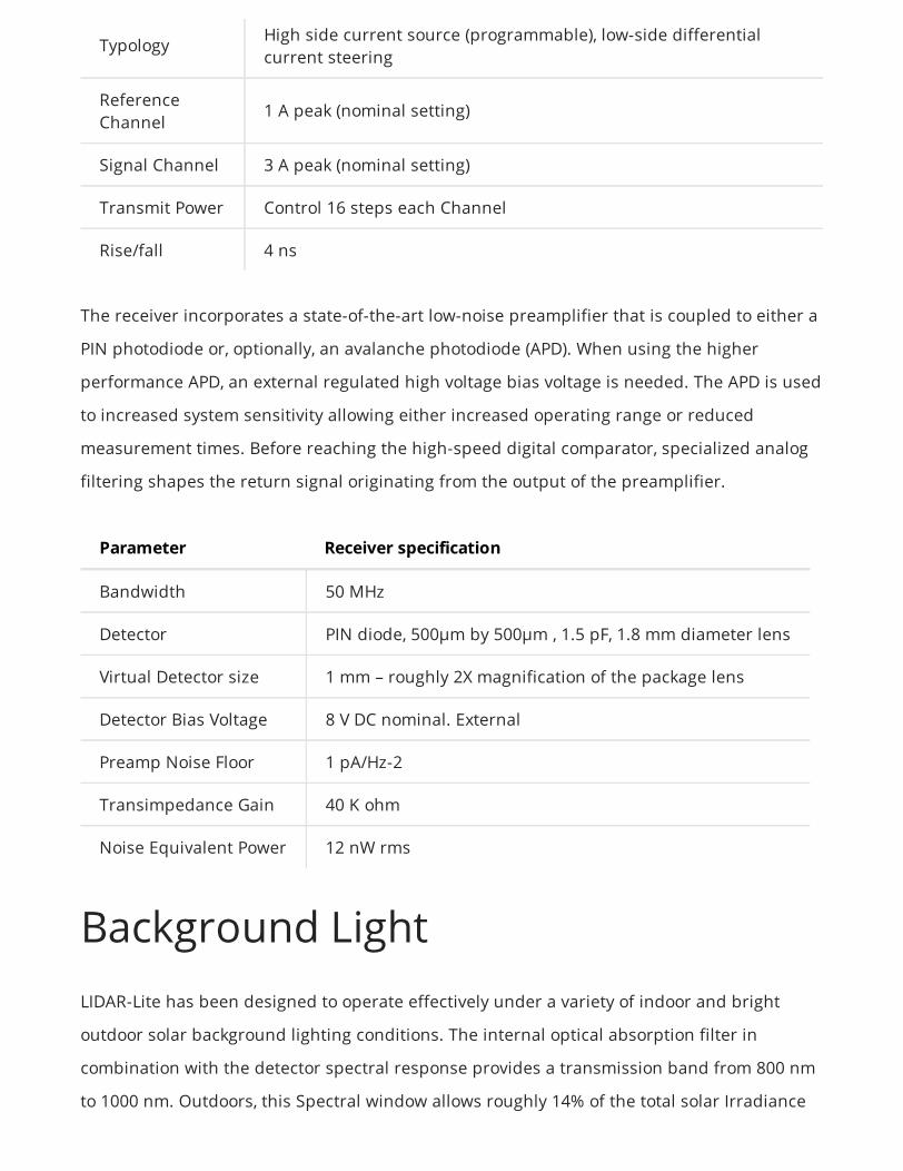
Typology High side current source (programmable), low-side differentialcurrent steering
ReferenceChannel
1 A peak (nominal setting)
Signal Channel 3 A peak (nominal setting)
Transmit Power Control 16 steps each Channel
Rise/fall 4 ns
The receiver incorporates a state-of-the-art low-noise preamplifier that is coupled to either a
PIN photodiode or, optionally, an avalanche photodiode (APD). When using the higher
performance APD, an external regulated high voltage bias voltage is needed. The APD is used
to increased system sensitivity allowing either increased operating range or reduced
measurement times. Before reaching the high-speed digital comparator, specialized analog
filtering shapes the return signal originating from the output of the preamplifier.
Parameter Receiver specification
Bandwidth 50 MHz
Detector PIN diode, 500µm by 500µm , 1.5 pF, 1.8 mm diameter lens
Virtual Detector size 1 mm – roughly 2X magnification of the package lens
Detector Bias Voltage 8 V DC nominal. External
Preamp Noise Floor 1 pA/Hz-2
Transimpedance Gain 40 K ohm
Noise Equivalent Power 12 nW rms
Background LightLIDAR-Lite has been designed to operate effectively under a variety of indoor and bright
outdoor solar background lighting conditions. The internal optical absorption filter in
combination with the detector spectral response provides a transmission band from 800 nm
to 1000 nm. Outdoors, this Spectral window allows roughly 14% of the total solar Irradiance
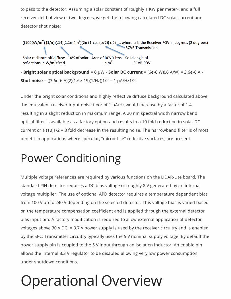
to pass to the detector. Assuming a solar constant of roughly 1 KW per meter², and a full
receiver field of view of two degrees, we get the following calculated DC solar current and
detector shot noise:
- Bright solar optical background = 6 µW - Solar DC current = (6e-6 W)(.6 A/W) = 3.6e-6 A -
Shot noise = ((3.6e-6 A)(2)(1.6e-19)(1/Hz))1/2 = 1 pA/Hz1/2
Under the bright solar conditions and highly reflective diffuse background calculated above,
the equivalent receiver input noise floor of 1 pA/Hz would increase by a factor of 1.4
resulting in a slight reduction in maximum range. A 20 nm spectral width narrow band
optical filter is available as a factory option and results in a 10 fold reduction in solar DC
current or a (10)1/2 = 3 fold decrease in the resulting noise. The narrowband filter is of most
benefit in applications where specular, "mirror like" reflective surfaces, are present.
Power ConditioningMultiple voltage references are required by various functions on the LIDAR-Lite board. The
standard PIN detector requires a DC bias voltage of roughly 8 V generated by an internal
voltage multiplier. The use of optional APD detector requires a temperature dependent bias
from 100 V up to 240 V depending on the selected detector. This voltage bias is varied based
on the temperature compensation coefficient and is applied through the external detector
bias input pin. A factory modification is required to allow external application of detector
voltages above 30 V DC. A 3.7 V power supply is used by the receiver circuitry and is enabled
by the SPC. Transmitter circuitry typically uses the 5 V nominal supply voltage. By default the
power supply pin is coupled to the 5 V input through an isolation inductor. An enable pin
allows the internal 3.3 V regulator to be disabled allowing very low power consumption
under shutdown conditions.
Operational Overview
Operation of LIDAR-Lite can be separated into two phases; initialization and triggered
acquisitions as initiated by the user.
During initialization the microcontroller goes through a self-test sequence followed by
initialization of the internal control registers with default values. Internal control registers
can be customized by the user through the I2C interface after initialization. After the internal
control registers are initialized the processor goes into sleep state reducing overall power
consumption to under 10 mA. Initiation of a user command, through external trigger or I2C
command, awakes a processor allowing subsequent operation.
The input of a command through the I2C interfaces may initiate an acquisition or an
operation to monitor or modify system parameters. In the event of an acquisition request,
the system must first power up and initialize the external functions such as the SPC and
transmit/receive circuitry. Acquisition begins with the transmission of a reference burst
followed by a signal burst. These signal bursts occur over intervals of roughly 50- 100µs
depending on the length of the selected correlation record. These signal bursts are repeated
until the maximum number of acquisitions have been reached, as defined in the default or
user settings or a sufficient number of acquisitions have been performed to achieve a
maximum signal strength level. At the completion of the required number of acquisition
cycles, the correlation results are processed to calculate the effective time delay of the
reference and return within the correlation records. The total acquisition time for the
reference and signal acquisitions is typically between 5 and 20ms depending on the desired
number of integrated pulses and the length of the correlation record. The acquisition time
plus the required 1 msec to download measurement parameters establish a roughly 100Hz
maximum measurement rate.
Mode Control PinA bi-directional control and status pin provides a means to trigger acquisitions and return
the measured distance via Pulse Width Modulation [PWM] without having to use the I2C
interface.
The pin driver in the processor has an internal current source pull-up of roughly 50uA with
the driver output coupled to the user pin through a protection diode allowing only sourcing
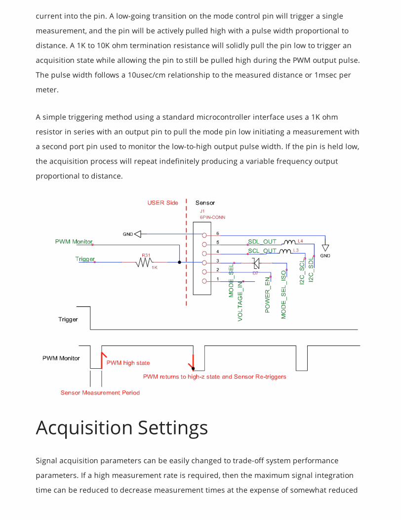
current into the pin. A low-going transition on the mode control pin will trigger a single
measurement, and the pin will be actively pulled high with a pulse width proportional to
distance. A 1K to 10K ohm termination resistance will solidly pull the pin low to trigger an
acquisition state while allowing the pin to still be pulled high during the PWM output pulse.
The pulse width follows a 10usec/cm relationship to the measured distance or 1msec per
meter.
A simple triggering method using a standard microcontroller interface uses a 1K ohm
resistor in series with an output pin to pull the mode pin low initiating a measurement with
a second port pin used to monitor the low-to-high output pulse width. If the pin is held low,
the acquisition process will repeat indefinitely producing a variable frequency output
proportional to distance.
Acquisition SettingsSignal acquisition parameters can be easily changed to trade-off system performance
parameters. If a high measurement rate is required, then the maximum signal integration
time can be reduced to decrease measurement times at the expense of somewhat reduced

sensitivity and maximum range. Optical transmit power can be increased by the setting
loaded into the Laser Power Register. High pulse power may need to be compensated with
an increased spacing between pulse bursts to maintain an acceptable laser duty cycle based
on thermal derating requirements. If the length of the correlation record is increased to
allow for longer range measurements, increased processing time will decrease the
measurement rate.
Key control registers impacting acquisitions:
Internal register space
Register Description
control_reg[2]
Maximum acquisition count sets the maximum number of acquisitioncycles with a maximum value of 255. In most cases an acquisition of 128is adequate.
control_reg[3]
Correlation record length establishes the portion of correlation memoryallocated to the return signal. The value is broken in to upper and lowernibbles where the lower indicates the starting location and the uppernibble the end point. The nibble value multiplied by 64 is its location inmemory. A value of 0xf indicates the end of the record with a value of1024.
control_reg[4]
Acquisition mode control establish the enabled acquisition functionssuch as velocity measurement, lower power consumption states andinhibiting the reference.
External register space
Register Desciption
control_reg[0x43]
Laser power control.
control_reg[0x4b]
Range Processing Criteria for two echoes. Max signal, Max/MinRange.
control_reg[0x65]
Power management – Sleep states.
Signal Acquisition ProcessAfter loading new acquisition parameters or retaining default values, a command is sent to
the SPC to initiate a signal acquisition. The steps of the acquisition are as follows: 1. Power is
applied to the receiver preamp and, after a prescribed delay, the DC offset at the threshold
detector is adjusted to set the effective slicing level or threshold in the middle of the noise
distribution. The adjustment process is based on the measurement of the one/zero duty
cycle at the comparator output. When the signal offset is nulled, the duty cycle of the noise
pattern approaches an average of 50%. In more sophisticated applications the threshold can
be offset as part of an algorithm to measure the approximate rms value of the noise
supporting diagnostics or as part of a voltage control feedback signal supporting an
avalanche photo detector biasing. 2. Prior to starting signal acquisition, the correlation
memory is cleared and the transmitter is activated to generate a burst signal pattern that is
stored in a signature memory that is used as key element in the correlation process. 3. Signal
acquisition begins with the activation of the reference portion of the transmitter, followed by
the feeding of the signal pattern necessary to generate the optical reference signal which
then passes directly to the receiver photo detector. After amplification and zero-crossing
detection, this record is stored in the signal memory. 4. The stored reference signal record is
then correlation processed using the transmit pattern stored in the signature memory as a
template which is then added to any correlation data previously processed and residing the
reference portion of the correlation memory. 5. Next the signal transmit portion of the
transmitter is enabled and the outgoing optical signal goes out to a target and the signal
return is amplified, detected and stored in signal memory. 6. As in step 4, the stored signal
record is correlation processed and then added to any correlation data previously processed
and residing in the signal portion of the correlation memory. 7. As the signal and reference
acquisitions are repeated, the peak correlation values in the correlation record increase and
would ultimately overflow the 12-bit word size. To prevent this overflow condition, the
correlation process is terminated for either the signal or reference records when a peak
signal within the record exceeds a preset maximum value slightly under overflow. Once both
the reference and signal records have reached their maximum values or that maximum
acquisition count has been exceeded the acquisition process is terminated. 8. After the
signal acquisition process is complete, a low-pass and DC restoring filtering process typically
cleans-up the waveform to improve the final measurement accuracy at low signal conditions
and short range. This function can be disabled by resetting the filter enable bit in control
register 4 for improved accuracy and resolution at longer ranges.
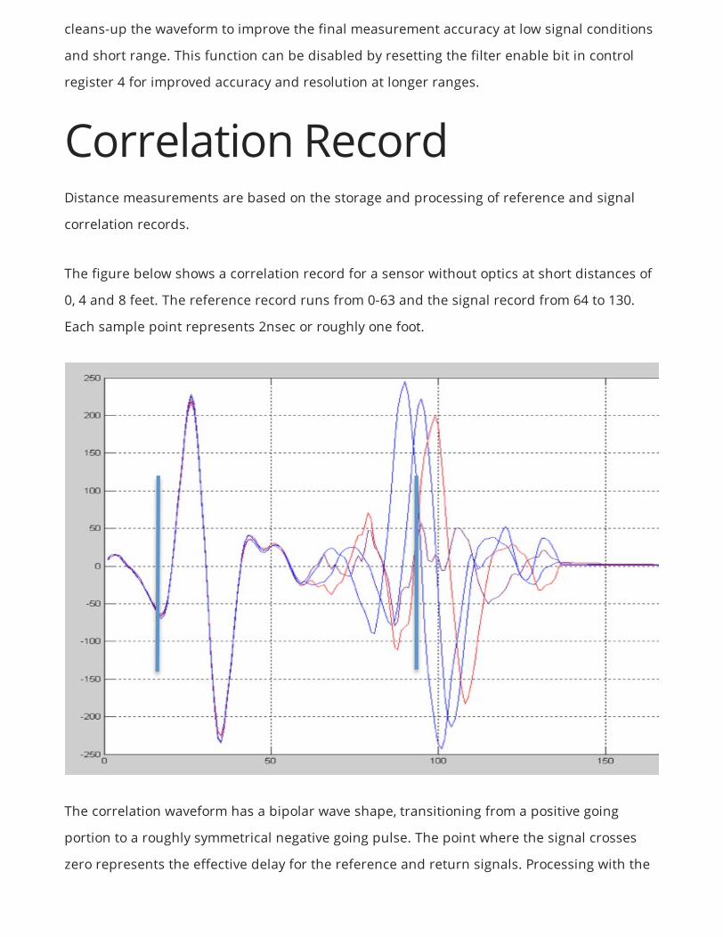
Correlation RecordDistance measurements are based on the storage and processing of reference and signal
correlation records.
The figure below shows a correlation record for a sensor without optics at short distances of
0, 4 and 8 feet. The reference record runs from 0-63 and the signal record from 64 to 130.
Each sample point represents 2nsec or roughly one foot.
The correlation waveform has a bipolar wave shape, transitioning from a positive going
portion to a roughly symmetrical negative going pulse. The point where the signal crosses
zero represents the effective delay for the reference and return signals. Processing with the
SPC determines the interpolated crossing point to a 1cm resolution along with the peak
signal value.
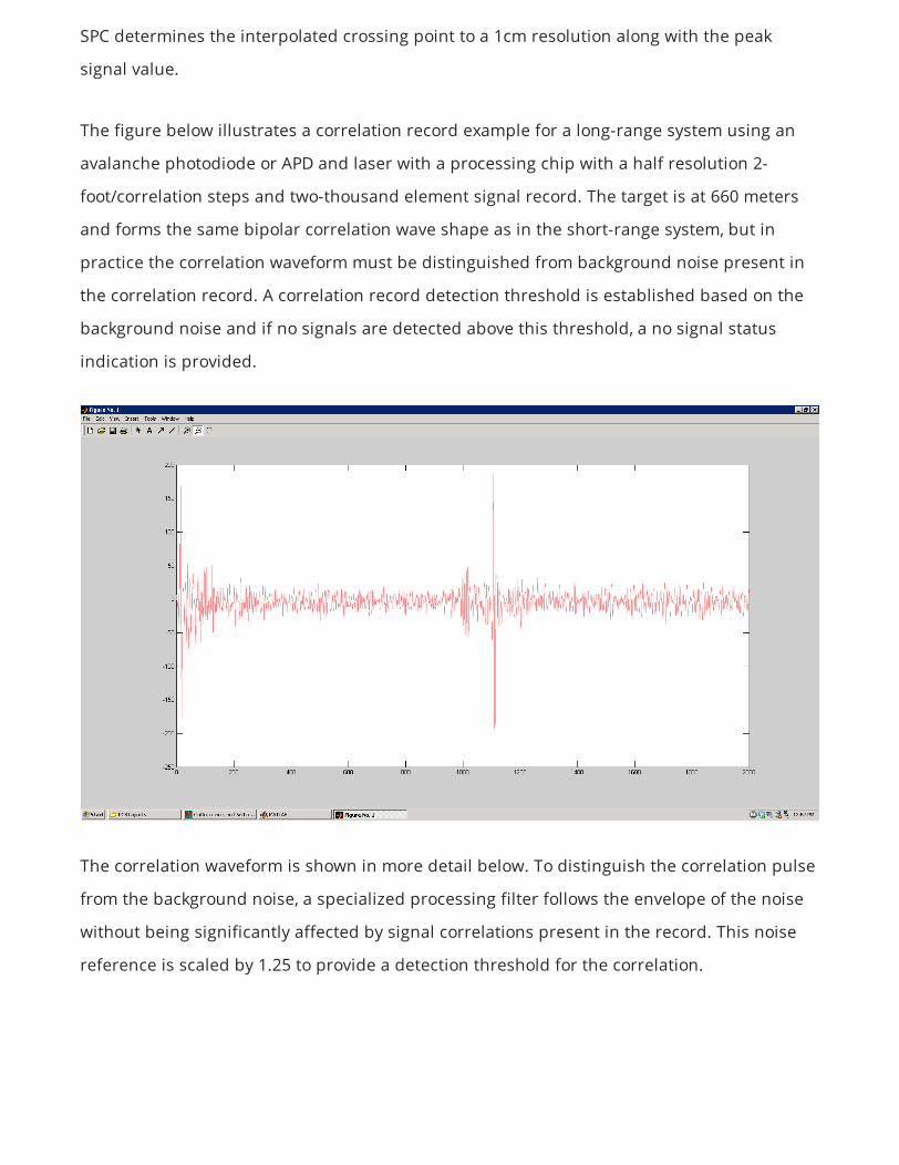
The figure below illustrates a correlation record example for a long-range system using an
avalanche photodiode or APD and laser with a processing chip with a half resolution 2-
foot/correlation steps and two-thousand element signal record. The target is at 660 meters
and forms the same bipolar correlation wave shape as in the short-range system, but in
practice the correlation waveform must be distinguished from background noise present in
the correlation record. A correlation record detection threshold is established based on the
background noise and if no signals are detected above this threshold, a no signal status
indication is provided.
The correlation waveform is shown in more detail below. To distinguish the correlation pulse
from the background noise, a specialized processing filter follows the envelope of the noise
without being significantly affected by signal correlations present in the record. This noise
reference is scaled by 1.25 to provide a detection threshold for the correlation.
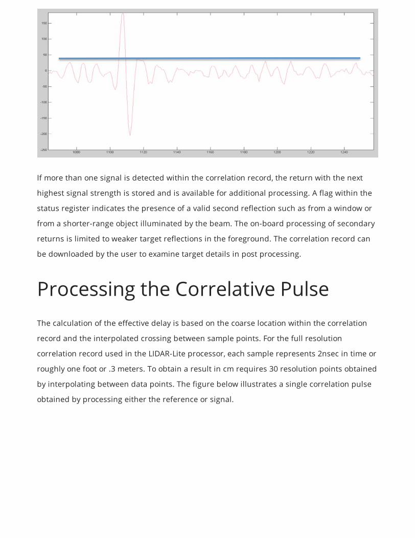
If more than one signal is detected within the correlation record, the return with the next
highest signal strength is stored and is available for additional processing. A flag within the
status register indicates the presence of a valid second reflection such as from a window or
from a shorter-range object illuminated by the beam. The on-board processing of secondary
returns is limited to weaker target reflections in the foreground. The correlation record can
be downloaded by the user to examine target details in post processing.
Processing the Correlative PulseThe calculation of the effective delay is based on the coarse location within the correlation
record and the interpolated crossing between sample points. For the full resolution
correlation record used in the LIDAR-Lite processor, each sample represents 2nsec in time or
roughly one foot or .3 meters. To obtain a result in cm requires 30 resolution points obtained
by interpolating between data points. The figure below illustrates a single correlation pulse
obtained by processing either the reference or signal.
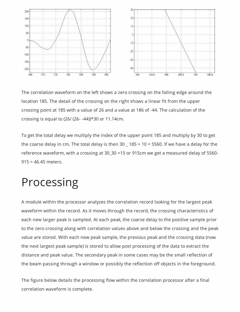
The correlation waveform on the left shows a zero crossing on the falling edge around the
location 185. The detail of the crossing on the right shows a linear fit from the upper
crossing point at 185 with a value of 26 and a value at 186 of -44. The calculation of the
crossing is equal to (26/ (26- -44))*30 or 11.14cm.
To get the total delay we multiply the index of the upper point 185 and multiply by 30 to get
the coarse delay in cm. The total delay is then 30 _ 185 + 10 = 5560. If we have a delay for the
reference waveform, with a crossing at 30_30 +15 or 915cm we get a measured delay of 5560-
915 = 46.45 meters.
ProcessingA module within the processor analyzes the correlation record looking for the largest peak
waveform within the record. As it moves through the record, the crossing characteristics of
each new larger peak is sampled. At each peak, the coarse delay to the positive sample prior
to the zero crossing along with correlation values above and below the crossing and the peak
value are stored. With each new peak sample, the previous peak and the crossing data (now
the next largest peak sample) is stored to allow post processing of the data to extract the
distance and peak value. The secondary peak in some cases may be the small reflection of
the beam passing through a window or possibly the reflection off objects in the foreground.
The figure below details the processing flow within the correlation processor after a final
correlation waveform is complete.
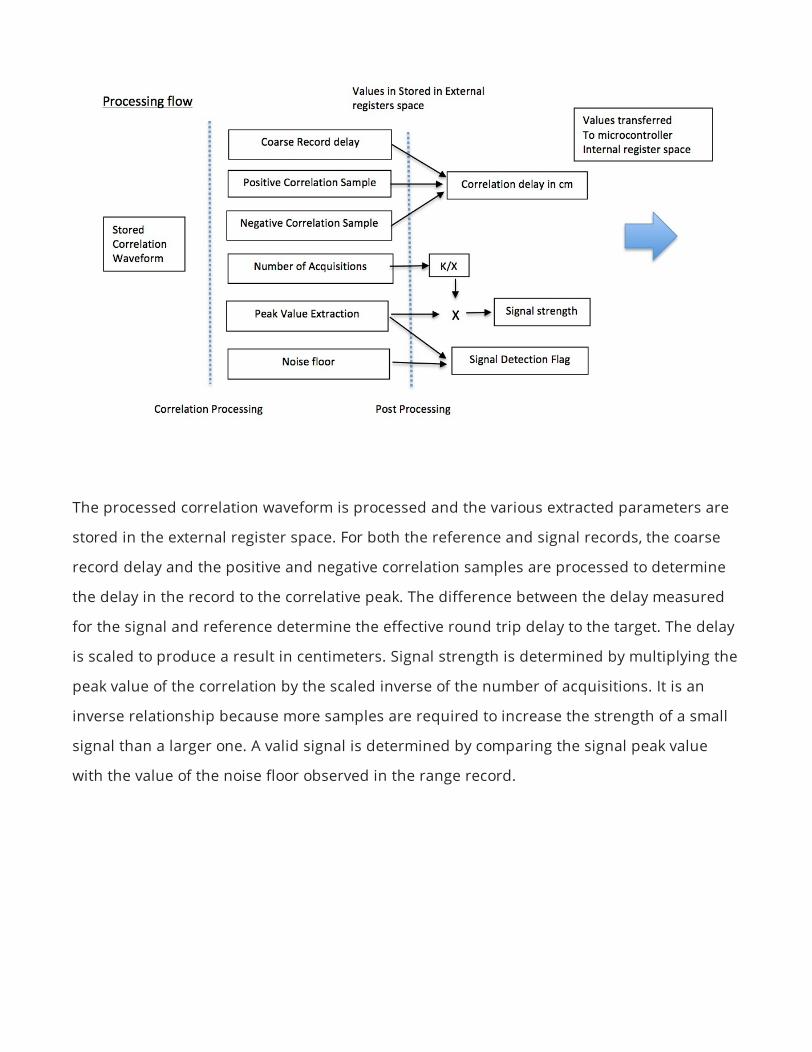
The processed correlation waveform is processed and the various extracted parameters are
stored in the external register space. For both the reference and signal records, the coarse
record delay and the positive and negative correlation samples are processed to determine
the delay in the record to the correlative peak. The difference between the delay measured
for the signal and reference determine the effective round trip delay to the target. The delay
is scaled to produce a result in centimeters. Signal strength is determined by multiplying the
peak value of the correlation by the scaled inverse of the number of acquisitions. It is an
inverse relationship because more samples are required to increase the strength of a small
signal than a larger one. A valid signal is determined by comparing the signal peak value
with the value of the noise floor observed in the range record.