Embed Size (px)
Citation preview

Technology Focus
Computers/Electronics
Software
Materials
Mechanics
Machinery/Automation
Manufacturing
Bio-Medical
Physical Sciences
Information Sciences
Books and Reports
05-03 May 2003
https://ntrs.nasa.gov/search.jsp?R=20110023805 2018-05-27T03:44:21+00:00Z

INTRODUCTIONTech Briefs are short announcements of innovations originating from research and develop-
ment activities of the National Aeronautics and Space Administration. They emphasizeinformation considered likely to be transferable across industrial, regional, or disciplinary linesand are issued to encourage commercial application.
Availability of NASA Tech Briefs and TSPsRequests for individual Tech Briefs or for Technical Support Packages (TSPs) announced herein shouldbe addressed to
National Technology Transfer CenterTelephone No. (800) 678-6882 or via World Wide Web at www2.nttc.edu/leads/
Please reference the control numbers appearing at the end of each Tech Brief. Information on NASA’s Commercial Technology Team, its documents, and services is also available at the same facility or on the World Wide Web at www.nctn.hq.nasa.gov.
Commercial Technology Offices and Patent Counsels are located at NASA field centers to providetechnology-transfer access to industrial users. Inquiries can be made by contacting NASA field centersand program offices listed below.
Ames Research CenterCarolina Blake(650) [email protected]
Dryden Flight Research CenterJenny Baer-Riedhart(661) [email protected]
Goddard Space Flight CenterNona Cheeks(301) [email protected]
Jet Propulsion LaboratoryArt Murphy, Jr.(818) [email protected]
Johnson Space CenterCharlene E. Gilbert(281) [email protected]
Kennedy Space CenterJim Aliberti(321) [email protected]
Langley Research CenterSam Morello(757) [email protected]
John H. Glenn Research Center atLewis FieldLarry Viterna(216) [email protected]
Marshall Space Flight CenterVernotto McMillan(256) [email protected]
Stennis Space CenterRobert Bruce(228) [email protected]
Carl RaySmall Business InnovationResearch Program (SBIR) &Small Business TechnologyTransfer Program (STTR)(202) 358-4652 [email protected]
Dr. Robert NorwoodOffice of CommercialTechnology (Code RW)(202) 358-2320 [email protected]
John MankinsOffice of Space Flight (Code MP)(202) 358-4659 [email protected]
Terry HertzOffice of Aero-SpaceTechnology (Code RS)(202) 358-4636 [email protected]
Glen MucklowOffice of Space Sciences(Code SM)(202) 358-2235 [email protected]
Roger CrouchOffice of Microgravity ScienceApplications (Code U)(202) 358-0689 [email protected]
Granville PaulesOffice of Mission to Planet Earth(Code Y) (202) 358-0706 [email protected]
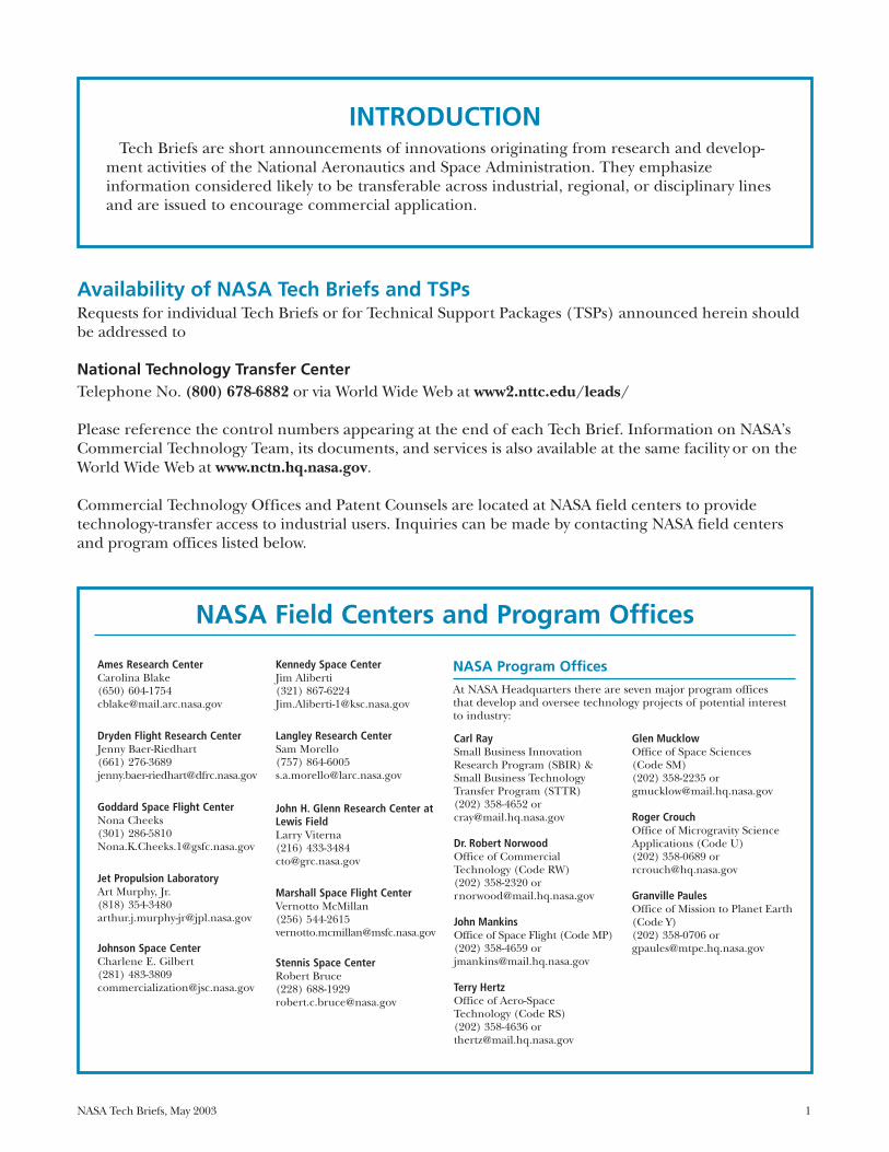
NASA Field Centers and Program Offices
NASA Program Offices
At NASA Headquarters there are seven major program offices that develop and oversee technology projects of potential interest to industry:
NASA Tech Briefs, May 2003 1


5 Technology Focus: Sensors
5 Using Diffusion Bonding in Making PiezoelectricActuators
6 Wireless Temperature-Monitoring System
7 Analog Binaural Circuits for Detecting andLocating Leaks
7 Mirrors Containing Biomimetic Shape-ControlActuators
9 Computers/Electronics
9 Surface-Micromachined Planar Arrays ofThermopiles
10 Cascade Back-Propagation Learning in NeuralNetworks
13 Materials
13 Perovskite Superlattices as Tunable MicrowaveDevices
14 Rollable Thin-Shell Nanolaminate Mirrors
15 Mechanics
15 Flight Tests of a Ministick Controller in an F/A-18Airplane
16 Piezoelectrically Actuated Shutter for HighVacuum
17 Machinery/Automation
17 Bio-Inspired Engineering of Exploration Systems
19 Manufacturing
19 Microscope Cells Containing MultipleMicromachined Wells
20 Electrophoretic Deposition for FabricatingMicrobatteries
21 Physical Sciences
21 Integrated Arrays of Ion-Sensitive Electrodes
22 Model of Fluidized Bed Containing ReactingSolids and Gases
23 Membrane Mirrors With Bimorph ShapeActuators
25 Information Sciences
25 Using Fractional Clock-Period Delays in TelemetryArraying
26 Developing Generic Software for SpacecraftAvionics
27 Books & Reports
27 Numerical Study of Pyrolysis of Biomass inFluidized Beds
27 Assessment of Models of Chemically ReactingGranular Flows
05-03 May 2003
This document was prepared under the sponsorship of the National Aeronautics and Space Administration. Neither the United States Governmentnor any person acting on behalf of the United States Government assumes any liability resulting from the use of the information contained in thisdocument, or warrants that such use will be free from privately owned rights.
NASA Tech Briefs, May 2003 3

NASA Tech Briefs, May 2003 5
A technique for the fabrication ofpiezoelectric actuators that generateacceptably large forces and deflectionsat relatively low applied voltages in-volves the stacking and diffusion bond-ing of multiple thin piezoelectric layerscoated with film electrodes. The pres-ent technique stands in contrast to anolder technique in which the layers arebonded chemically, by use of urethaneor epoxy agents.
The older chemical-bonding tech-nique entails several disadvantages, in-cluding the following:• It is difficult to apply the bonding
agents to the piezoelectric layers.• It is difficult to position the layers ac-
curately and without making mistakes.• There is a problem of disposal of haz-
ardous urethane and epoxy wastes.• The urethane and epoxy agents are
nonpiezoelectric materials. As such,they contribute to the thickness of a
piezoelectric laminate without con-tributing to its performance; con-versely, for a given total thickness, theperformance of the laminate is belowthat of a unitary piezoelectric plate ofthe same thickness.The figure depicts some aspects of
the fabrication of a laminated piezo-electric actuator by the present diffu-sion-bonding technique. First, stocksheets of the piezoelectric material areinspected and tested. Next, the holepattern shown in the figure is punchedinto the sheets. Alternatively, if thepiezoelectric material is not a polymer,then the holes are punched in thermo-plastic films. Then both faces of eachpunched piezoelectric sheet or thermo-plastic film are coated with a silver-inkelectrode material by use of a silk-screen printer. The electrode and holepatterns are designed for minimal com-plexity and minimal waste of material.
After a final electrical test, all thecoated piezoelectric layers (or piezoelec-tric layers and coated thermoplasticfilms) are stacked in an alignment jig,which, in turn, is placed in a curvedpress for the diffusion-bonding process.In this process, the stack is pressed andheated at a specified curing temperatureand pressure for a specified curing time.The pressure, temperature, and time de-pend on the piezoelectric material se-lected. At the end of the diffusion-bond-ing process, the resulting laminatedpiezoelectric actuator is tested to verifythe adequacy of the mechanical outputas a function of an applied DC voltage.
The principal advantages of the diffu-sion-bonding process over the olderchemical-bonding process are the fol-lowing:• No adhesive thinner or hardening
agent is needed;• There are no waste chemicals;
Technology Focus: Sensors
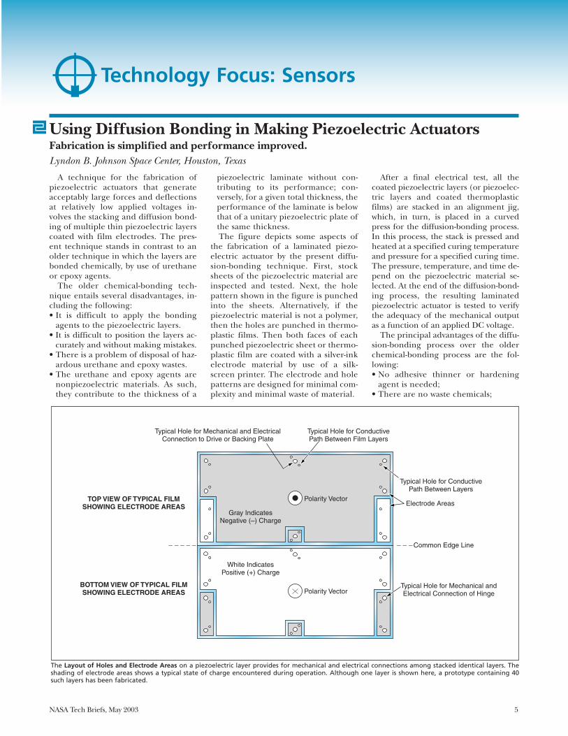
Typical Hole for Mechanical and ElectricalConnection to Drive or Backing Plate
Typical Hole for Mechanical andElectrical Connection of Hinge
White IndicatesPositive (+) Charge
Gray IndicatesNegative (–) Charge
Polarity Vector
Polarity Vector
Typical Hole for ConductivePath Between Film Layers
Typical Hole for ConductivePath Between Layers
TOP VIEW OF TYPICAL FILMSHOWING ELECTRODE AREAS
BOTTOM VIEW OF TYPICAL FILMSHOWING ELECTRODE AREAS
Electrode Areas
Common Edge Line
Using Diffusion Bonding in Making Piezoelectric ActuatorsFabrication is simplified and performance improved.Lyndon B. Johnson Space Center, Houston, Texas
The Layout of Holes and Electrode Areas on a piezoelectric layer provides for mechanical and electrical connections among stacked identical layers. Theshading of electrode areas shows a typical state of charge encountered during operation. Although one layer is shown here, a prototype containing 40such layers has been fabricated.
6 NASA Tech Briefs, May 2003
• Cure can be done at a relatively lowtemperature;
• There is less handling of piezoelectricsheets;
• No special adhesive-handling equip-ment is needed;
• The thickness contributed by the ther-moplastic adhesive material (if used)is minimal;
• Diffusion bonding results in high-strength bonds that impart high dura-bility and long fatigue life.
• In the case of polymeric piezoelectriclayers, piezoelectric properties areimproved, probably because of an in-crease in Young’s modulus associated
with annealing during diffusionbonding.
• There is a significant reduction inelectrical wiring: The electrode andhole patterns in the stacked layersgive rise to an internal topologyequivalent to that of a continuouslyfolded length of piezoelectric mate-rial. As a result, the multiple electri-cal connections to the active piezo-electric layers are reduced to twoterminal holes.This work was done by Frank E. Sager of
Oceaneering Space Systems for JohnsonSpace Center. Further information is con-tained in a TSP (see page 1).
Title to this invention, covered by U.S.Patent No. 5,761,782 has been waived underthe provisions of the National Aeronauticsand Space Act 42 U.S.C. 2457 (f). In-quiries concerning licenses for its commercialdevelopment should be addressed to
Mr. Jeff BrownOceaneering Space Systems16665 Space Center Blvd.Houston , TX 77598Tel. No: (281) 488-9080 Ext. 3437Fax No: (281) 488-6485Refer to MSC-22886, volume and number
of this NASA Tech Briefs issue, and thepage number.
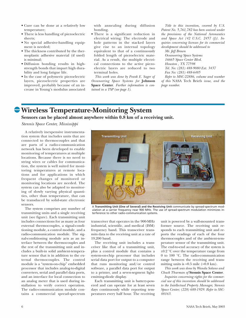
Wireless Temperature-Monitoring SystemSensors can be placed almost anywhere within 0.8 km of a receiving unit.Stennis Space Center, Mississippi
A relatively inexpensive instrumenta-tion system that includes units that areconnected to thermocouples and thatare parts of a radio-communicationnetwork has been developed to enablemonitoring of temperatures at multiplelocations. Because there is no need tostring wires or cables for communica-tion, the system is well suited for moni-toring temperatures at remote loca-tions and for applications in whichfrequent changes of monitored ormonitoring locations are needed. Thesystem can also be adapted to monitor-ing of slowly varying physical quanti-ties, other than temperature, that canbe transduced by solid-state electronicsensors.
The system comprises any number oftransmitting units and a single receivingunit (see figure). Each transmitting unitincludes connections for as many as fourexternal thermocouples, a signal-condi-tioning module, a control module, and aradio-communication module. The sig-nal-conditioning module acts as an in-terface between the thermocouples andthe rest of the transmitting unit and in-cludes a built-in solid ambient-tempera-ture sensor that is in addition to the ex-ternal thermocouples. The controlmodule is a “system-on-chip” embeddedprocessor that includes analog-to-digitalconverters, serial and parallel data ports,and an interface for local connection toan analog meter that is used during in-stallation to verify correct operation.The radio-communication module con-tains a commercial spread-spectrum
transceiver that operates in the 900-MHzindustrial, scientific, and medical (ISM)frequency band. This transceiver trans-mits data to the receiving unit at a rate of19,200 baud.
The receiving unit includes a trans-ceiver like that of a transmitting unit,plus a control module that contains asystem-on-chip processor that includesserial data port for output to a computerthat runs monitoring and/or controlsoftware, a parallel data port for outputto a printer, and a seven-segment light-emitting-diode display.
Each transmitting unit is battery-pow-ered and can operate for at least sevendays continuously while reporting tem-peratures every half hour. The receiving
unit is powered by a wall-mounted trans-former source. The receiving unit re-sponds to each transmitting unit and re-ports the readings of each of the fourthermocouples and of the ambient-tem-perature sensor of the transmitting unit.The end-to-end accuracy of the system is±0.2 °C over the temperature range from0 to 100 °C. The radio-communicationrange between the receiving and trans-mitting units is ≈0.5 mile (≈0.8 km).
This work was done by Wanda Solano andChuck Thurman of Stennis Space Center.
Inquiries concerning rights for the commer-cial use of this invention should be addressedto the Intellectual Property Manager, StennisSpace Center; (228) 688-1929. Refer to SSC-00163.
Transmitting Unit Receiving UnitTransmitting Unit Receiving Unit
A Transmitting Unit (One of Several) and the Receiving Unit communicate by spread-spectrum mod-ulation at a carrier frequency near 900 MHz. The use of spread-spectrum modulation minimizes in-terference to other radio-communication systems.

NASA Tech Briefs, May 2003 7
Analog Binaural Circuits for Detecting and Locating LeaksUltrasonic signals received by paired transducers would be correlated to measure differential delays.NASA’s Jet Propulsion Laboratory, Pasadena, California
Very-large-scale integrated (VLSI) ana-log binaural signal-processing circuitshave been proposed for use in detectingand locating leaks that emit noise in theultrasonic frequency range. These cir-cuits would be designed to function evenin the presence of intense lower-fre-quency background noise that could in-clude sounds associated with flow andpumping. Each of the proposed circuitswould include the approximate elec-tronic equivalent of a right and a leftcochlea plus correlator circuits.
A pair of transducers (microphonesor accelerometers), corresponding toright and left ears, would provide theinputs to their respective cochleas fromdifferent locations (e.g., from differentpositions along a pipe). The correlationcircuits plus some additional externalcircuits would determine the differencebetween the times of arrival of a com-mon leak sound at the two transducers.Then the distance along the pipe fromeither transducer to the leak could beestimated from the time difference andthe speed of sound along the pipe. Ifthree or more pairs of transducers andcochlear/correlator circuits were avail-able and could suitably be positioned, itshould be possible to locate a leak inthree dimensions by use of sound prop-agating through air.
The cochlear circuits would consistmostly of cascades of amplifier/delayunits positioned along two orthogonaledges of a rectangular VLSI chip, as de-picted in the figure in simplified form. Inaddition to introducing increments ofdelay, the cochlear circuits would filterthe signals to reject frequencies below theultrasonic range. The output of a givenamplifier/delay unit in a cochlea would
be fed to both the next amplifier/delayunit in the same cochlea and to a string ofcorrelator circuits, which would form theanalogs of the correlations between (1)the output of this unit and (2) the out-puts of all amplifier/delay units in theother cochlea. The outputs of the corre-lator circuits would be scanned by theexternal circuitry and displayed or oth-erwise processed to determine whichpairings of right and left cochlear units(and thus which differential signal
delay) yields the greatest correlations.This work was done by Frank T. Hartley of
Caltech for NASA’s Jet Propulsion Labo-ratory. Further information is contained in aTSP (see page 1).
This invention is owned by NASA, and apatent application has been filed. Inquiriesconcerning nonexclusive or exclusive licensefor its commercial development should be ad-dressed to the Patent Counsel, NASA Man-agement Office–JPL; (818) 354-7770. Referto NPO-18399.
RightMicrophone
LeftMicrophone
Correlator Circuits
CochlearAmplifier/
Delay Units
Cochlear and Correlator Circuits, operating in conjunction with external scanning circuits, would im-plement stereausis.
Curved mirrors of a proposed typewould comprise lightweight sheets orfilms containing integral, biologically in-spired actuators for controlling theirsurface figures. These mirrors could beuseful in such applications as collection
of solar energy, focusing of radio beams,and (provided sufficient precision couldbe achieved) imaging. These mirrorswere originally intended for use in outerspace, but it should also be possible todevelop terrestrial versions.
Several prior NASA Tech Briefs articleshave described a variety of approaches tothe design of curved, lightweight mirrorscontaining integral shape-control actua-tors. The primary distinction betweenthe present approach and the prior ap-
Mirrors Containing Biomimetic Shape-Control ActuatorsLocal bending would be controlled to obtain desired surface figures.NASA’s Jet Propulsion Laboratory, Pasadena, California
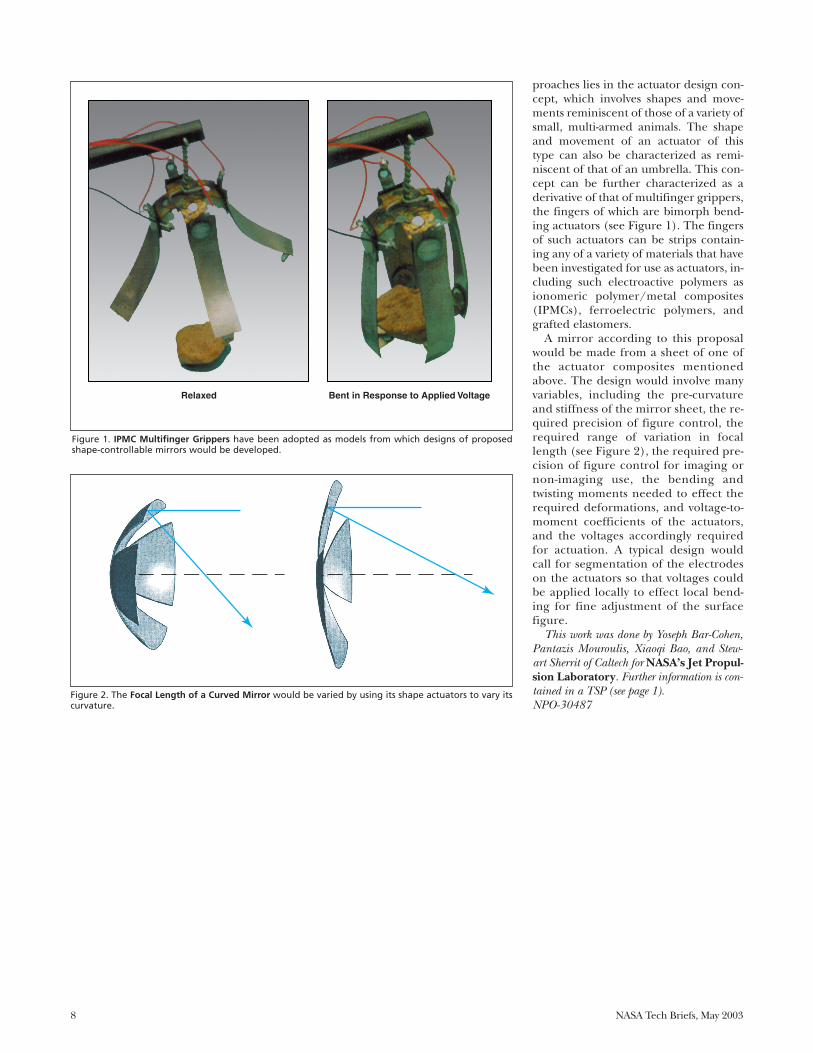
8 NASA Tech Briefs, May 2003
proaches lies in the actuator design con-cept, which involves shapes and move-ments reminiscent of those of a variety ofsmall, multi-armed animals. The shapeand movement of an actuator of thistype can also be characterized as remi-niscent of that of an umbrella. This con-cept can be further characterized as aderivative of that of multifinger grippers,the fingers of which are bimorph bend-ing actuators (see Figure 1). The fingersof such actuators can be strips contain-ing any of a variety of materials that havebeen investigated for use as actuators, in-cluding such electroactive polymers asionomeric polymer/metal composites(IPMCs), ferroelectric polymers, andgrafted elastomers.
A mirror according to this proposalwould be made from a sheet of one ofthe actuator composites mentionedabove. The design would involve manyvariables, including the pre-curvatureand stiffness of the mirror sheet, the re-quired precision of figure control, therequired range of variation in focallength (see Figure 2), the required pre-cision of figure control for imaging ornon-imaging use, the bending andtwisting moments needed to effect therequired deformations, and voltage-to-moment coefficients of the actuators,and the voltages accordingly requiredfor actuation. A typical design wouldcall for segmentation of the electrodeson the actuators so that voltages couldbe applied locally to effect local bend-ing for fine adjustment of the surfacefigure.
This work was done by Yoseph Bar-Cohen,Pantazis Mouroulis, Xiaoqi Bao, and Stew-art Sherrit of Caltech for NASA’s Jet Propul-sion Laboratory. Further information is con-tained in a TSP (see page 1).NPO-30487
Figure 2. The Focal Length of a Curved Mirror would be varied by using its shape actuators to vary itscurvature.
Relaxed Bent in Response to Applied Voltage
Figure 1. IPMC Multifinger Grippers have been adopted as models from which designs of proposedshape-controllable mirrors would be developed.
NASA Tech Briefs, May 2003 9
Computers/Electronics
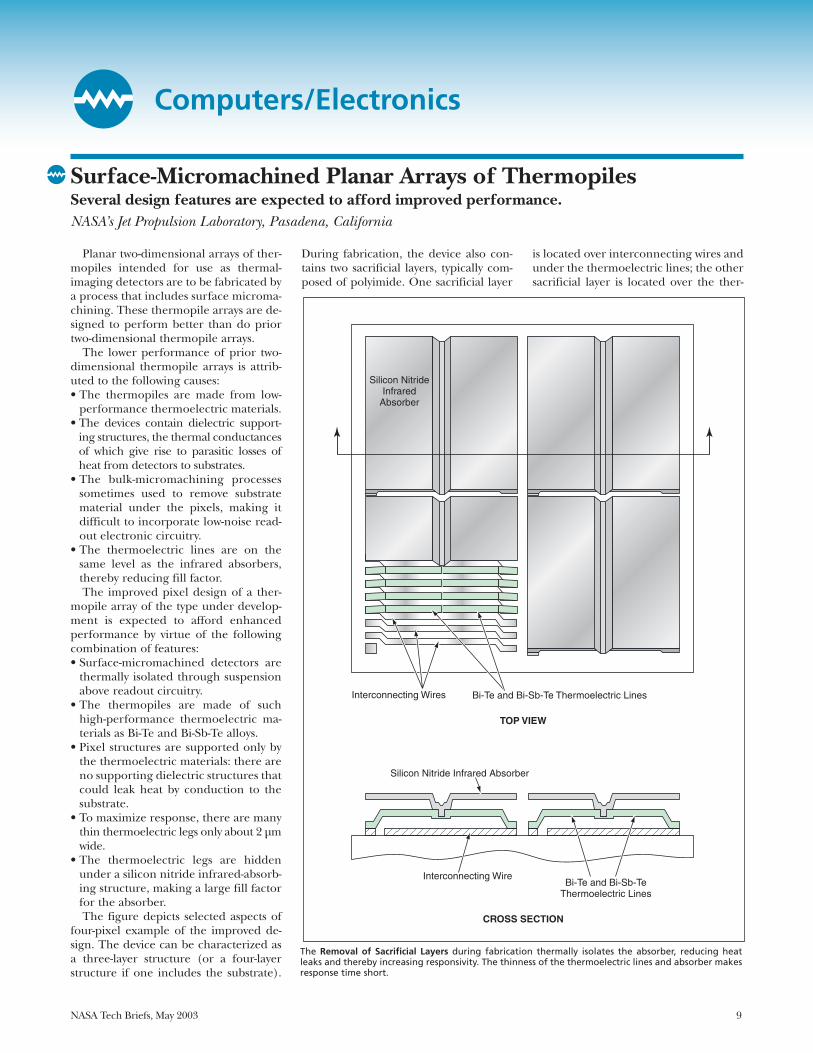
Surface-Micromachined Planar Arrays of ThermopilesSeveral design features are expected to afford improved performance.NASA’s Jet Propulsion Laboratory, Pasadena, California
Planar two-dimensional arrays of ther-mopiles intended for use as thermal-imaging detectors are to be fabricated bya process that includes surface microma-chining. These thermopile arrays are de-signed to perform better than do priortwo-dimensional thermopile arrays.
The lower performance of prior two-dimensional thermopile arrays is attrib-uted to the following causes:• The thermopiles are made from low-
performance thermoelectric materials.• The devices contain dielectric support-
ing structures, the thermal conductancesof which give rise to parasitic losses ofheat from detectors to substrates.
• The bulk-micromachining processessometimes used to remove substratematerial under the pixels, making itdifficult to incorporate low-noise read-out electronic circuitry.
• The thermoelectric lines are on thesame level as the infrared absorbers,thereby reducing fill factor.The improved pixel design of a ther-
mopile array of the type under develop-ment is expected to afford enhancedperformance by virtue of the followingcombination of features:• Surface-micromachined detectors are
thermally isolated through suspensionabove readout circuitry.
• The thermopiles are made of suchhigh-performance thermoelectric ma-terials as Bi-Te and Bi-Sb-Te alloys.
• Pixel structures are supported only bythe thermoelectric materials: there areno supporting dielectric structures thatcould leak heat by conduction to thesubstrate.
• To maximize response, there are manythin thermoelectric legs only about 2 µmwide.
• The thermoelectric legs are hiddenunder a silicon nitride infrared-absorb-ing structure, making a large fill factorfor the absorber.The figure depicts selected aspects of
four-pixel example of the improved de-sign. The device can be characterized asa three-layer structure (or a four-layerstructure if one includes the substrate).
During fabrication, the device also con-tains two sacrificial layers, typically com-posed of polyimide. One sacrificial layer
is located over interconnecting wires andunder the thermoelectric lines; the othersacrificial layer is located over the ther-
The Removal of Sacrificial Layers during fabrication thermally isolates the absorber, reducing heatleaks and thereby increasing responsivity. The thinness of the thermoelectric lines and absorber makesresponse time short.
Silicon NitrideInfrared
Absorber
Silicon Nitride Infrared Absorber
Bi-Te and Bi-Sb-Te Thermoelectric Lines
TOP VIEW
CROSS SECTION
Interconnecting WireBi-Te and Bi-Sb-Te
Thermoelectric Lines
Interconnecting Wires

10 NASA Tech Briefs, May 2003
moelectric lines and under the silicon ni-tride infrared absorber. After the detec-tor structure is fabricated, the sacrificiallayers are removed, typically by etchingin an oxygen plasma. The removal of thesacrificial layers is what provides the ther-mal isolation mentioned above.
The design facilitates maximization ofthe number of thermoelectric legs to in-crease the responsivity and the electricalimpedance of the detector. Using 2-µmwidths and 2-µm spacings of thermoelec-tric lines, it is possible to place about 11thermocouples under a 50-µm-wide pixel.
Absorption of infrared radiation is en-hanced by use of a quarter-wave cavity. In
each pixel, a thin layer of metal on thesilicon nitride layer constitutes a frontabsorber, while the thermoelectric legsand interconnecting wires, together,constitute a back-side mirror.
At the time of reporting the infor-mation for this article, partially com-pleted detectors (lacking the siliconnitride absorbers) of 100-µm pixel sizehad been built and tested. The resultsof the test indicate a pixel resistanceof 250 kΩ, responsivity of 1.5 kV/W,response time of 1.7 ms, and detectiv-ity (D*) of 2.4 × 108 cm⋅Hz1/2/W. Im-provements are ongoing.
This work was done by Marc C. Foote of
Caltech for NASA’s Jet Propulsion Labo-ratory. Further information is contained in aTSP (see page 1).
In accordance with Public Law 96-517, thecontractor has elected to retain title to this in-vention. Inquiries concerning rights for itscommercial use should be addressed to
Intellectual Property groupJPLMail Stop 202-2334800 Oak Grove DrivePasadena, CA 91109(818) 354-2240Refer to NPO-30124, volume and number
of this NASA Tech Briefs issue, and thepage number.
Cascade Back-Propagation Learning in Neural NetworksThis method would be implemented in VLSI circuitry.NASA’s Jet Propulsion Laboratory, Pasadena, California
The cascade back-propagation (CBP)algorithm is the basis of a conceptual de-sign for accelerating learning in artificialneural networks. The neural networkswould be implemented as analog very-large-scale integrated (VLSI) circuits,and circuits to implement the CBP algo-rithm would be fabricated on the sameVLSI circuit chips with the neural net-works. Heretofore, artificial neural net-works have learned slowly because it hasbeen necessary to train them via soft-ware, for lack of a good on-chip learningtechnique. The CBP algorithm is an on-chip technique that provides for contin-uous learning in real time.
Artificial neural networks are trainedby example: A network is presentedwith training inputs for which the cor-rect outputs are known, and the algo-rithm strives to adjust the weights ofsynaptic connections in the network tomake the actual outputs approach thecorrect outputs. The input data aregenerally divided into three parts. Twoof the parts, called the “training” and“cross-validation” sets, respectively,must be such that the correspondinginput/output pairs are known. Duringtraining, the cross-validation set en-ables verification of the status of theinput-to-output transformation learnedby the network to avoid overlearning.The third part of the data, termed the“test” set, consists of the inputs that arerequired to be transformed into out-puts; this set may or may not includethe training set and/or the cross-valida-tion set.
Proposed neural-network circuitry foron-chip learning would be divided intotwo distinct networks; one for trainingand one for validation. Both networkswould share the same synaptic weights.During training iterations, these weightswould be continuously modulated ac-cording to the CBP algorithm, which is
so named because it combines features ofthe back-propagation and cascade-corre-lation algorithms. Like other algorithmsfor learning in artificial neural networks,the CBP algorithm specifies an iterativeprocess for adjusting the weights ofsynaptic connections by descent alongthe gradient of an error measure in the
Start
Stop
Validating Network Training Network
Calculated Weightsby Pseudo-Inverse
Technique
Download Weights
Training Data
Add NewHidden Neuron
ReduceLearning
Rate
FreezeLearning
Rate
ComputeChanges
in Weights
LearningRate <
ThresholdLevel
Errors <Threshold
Level
Cross-ValidationData
PerformanceApplication(Test Sets)
No
No
Yes
Yes
Figure 1. The Cascade Back-Propagation Algorithm provides the theoretical basis for design of an ana-log neural network that learns rapidly.
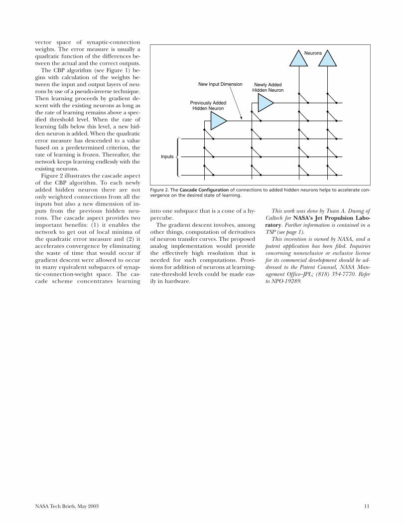
NASA Tech Briefs, May 2003 11
vector space of synaptic-connectionweights. The error measure is usually aquadratic function of the differences be-tween the actual and the correct outputs.
The CBP algorithm (see Figure 1) be-gins with calculation of the weights be-tween the input and output layers of neu-rons by use of a pseudo-inverse technique.Then learning proceeds by gradient de-scent with the existing neurons as long asthe rate of learning remains above a spec-ified threshold level. When the rate oflearning falls below this level, a new hid-den neuron is added. When the quadraticerror measure has descended to a valuebased on a predetermined criterion, therate of learning is frozen. Thereafter, thenetwork keeps learning endlessly with theexisting neurons.
Figure 2 illustrates the cascade aspectof the CBP algorithm. To each newlyadded hidden neuron there are notonly weighted connections from all theinputs but also a new dimension of in-puts from the previous hidden neu-rons. The cascade aspect provides twoimportant benefits: (1) it enables thenetwork to get out of local minima ofthe quadratic error measure and (2) itaccelerates convergence by eliminatingthe waste of time that would occur ifgradient descent were allowed to occurin many equivalent subspaces of synap-tic-connection-weight space. The cas-cade scheme concentrates learning
into one subspace that is a cone of a hy-percube.
The gradient descent involves, amongother things, computation of derivativesof neuron transfer curves. The proposedanalog implementation would providethe effectively high resolution that isneeded for such computations. Provi-sions for addition of neurons at learning-rate-threshold levels could be made eas-ily in hardware.
This work was done by Tuan A. Duong ofCaltech for NASA’s Jet Propulsion Labo-ratory. Further information is contained in aTSP (see page 1).
This invention is owned by NASA, and apatent application has been filed. Inquiriesconcerning nonexclusive or exclusive licensefor its commercial development should be ad-dressed to the Patent Counsel, NASA Man-agement Office–JPL; (818) 354-7770. Referto NPO-19289.
Neurons
Newly AddedHidden Neuron
New Input Dimension
Inputs
Previously AddedHidden Neuron
Figure 2. The Cascade Configuration of connections to added hidden neurons helps to accelerate con-vergence on the desired state of learning.

NASA Tech Briefs, May 2003 13
Experiments have shown that super-lattices that comprise alternating epi-taxial layers of dissimilar paraelectricperovskites can exhibit large changesin permittivity with the application ofelectric fields. The superlattices are po-tentially useful as electrically tunabledielectric components of such mi-crowave devices as filters and phaseshifters.
The electrically tunable materialsheretofore used in some microwave de-vices exhibit strong temperature depen-dences of dielectric properties and highmicrowave losses. Previous efforts toovercome these undesired effects haveinvolved the addition of variousdopants to SrTiO3, BaTiO3, andSrxBa1–xTiO3. Despite the amount of re-search in this area, results have beendisappointing.
The present superlattice approachdiffers fundamentally from the prior useof homogeneous, isotropic mixtures of
base materials and dopants. A superlat-tice can comprise layers of two or moreperovskites in any suitable sequence(e.g., ABAB…, ABCDABCD…, ABA-CABACA…). Even though a single layerof one of the perovskites by itself is nottunable, the compositions and sequenceof the layers can be chosen so that (1)the superlattice exhibits low microwaveloss and (2) the interfacial interactionbetween at least two of the perovskites inthe superlattice renders either the en-tire superlattice or else at least one ofthe perovskites tunable.
The perovskites investigated experi-mentally for use in superlattices in-clude SrTiO3, SrCeO3, SrZrO3,BaTiO3, BaZrO3, CaZrO3, and LaAlO3.Superlattices for the experiments werefabricated by pulsed laser depositiononto mostly LaAlO3 substrates; a fewspecimens were prepared on SrTiO3substrates. Microwave filters containingsuperlattices were also fabricated. The
superlattices were evaluated with re-spect to structure, composition, and di-electric properties.
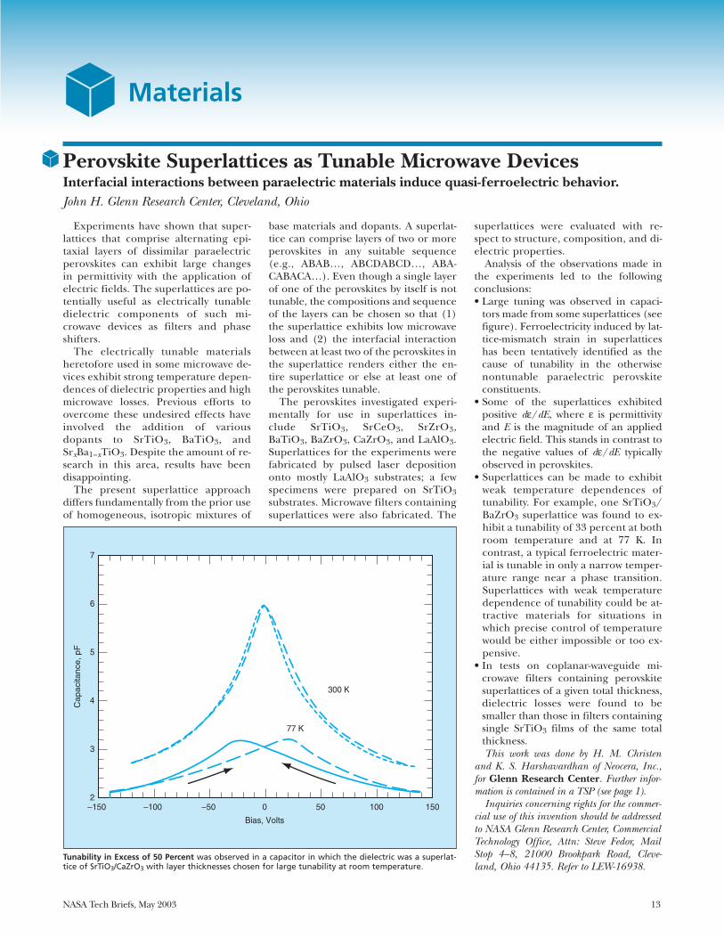
Analysis of the observations made inthe experiments led to the followingconclusions:• Large tuning was observed in capaci-
tors made from some superlattices (seefigure). Ferroelectricity induced by lat-tice-mismatch strain in superlatticeshas been tentatively identified as thecause of tunability in the otherwisenontunable paraelectric perovskiteconstituents.
• Some of the superlattices exhibitedpositive dε/dE, where ε is permittivityand E is the magnitude of an appliedelectric field. This stands in contrast tothe negative values of dε/dE typicallyobserved in perovskites.
• Superlattices can be made to exhibitweak temperature dependences oftunability. For example, one SrTiO3/BaZrO3 superlattice was found to ex-hibit a tunability of 33 percent at bothroom temperature and at 77 K. Incontrast, a typical ferroelectric mater-ial is tunable in only a narrow temper-ature range near a phase transition.Superlattices with weak temperaturedependence of tunability could be at-tractive materials for situations inwhich precise control of temperaturewould be either impossible or too ex-pensive.
• In tests on coplanar-waveguide mi-crowave filters containing perovskitesuperlattices of a given total thickness,dielectric losses were found to besmaller than those in filters containingsingle SrTiO3 films of the same totalthickness.This work was done by H. M. Christen
and K. S. Harshavardhan of Neocera, Inc.,for Glenn Research Center. Further infor-mation is contained in a TSP (see page 1).
Inquiries concerning rights for the commer-cial use of this invention should be addressedto NASA Glenn Research Center, CommercialTechnology Office, Attn: Steve Fedor, MailStop 4–8, 21000 Brookpark Road, Cleve-land, Ohio 44135. Refer to LEW-16938.
Tunability in Excess of 50 Percent was observed in a capacitor in which the dielectric was a superlat-tice of SrTiO3/CaZrO3 with layer thicknesses chosen for large tunability at room temperature.
Perovskite Superlattices as Tunable Microwave DevicesInterfacial interactions between paraelectric materials induce quasi-ferroelectric behavior.John H. Glenn Research Center, Cleveland, Ohio
–1502
3
4
5
6
7
–100 –50 0
Bias, Volts
Capaci
tance
, pF
50 100
300 K
77 K
150
Materials
14 NASA Tech Briefs, May 2003
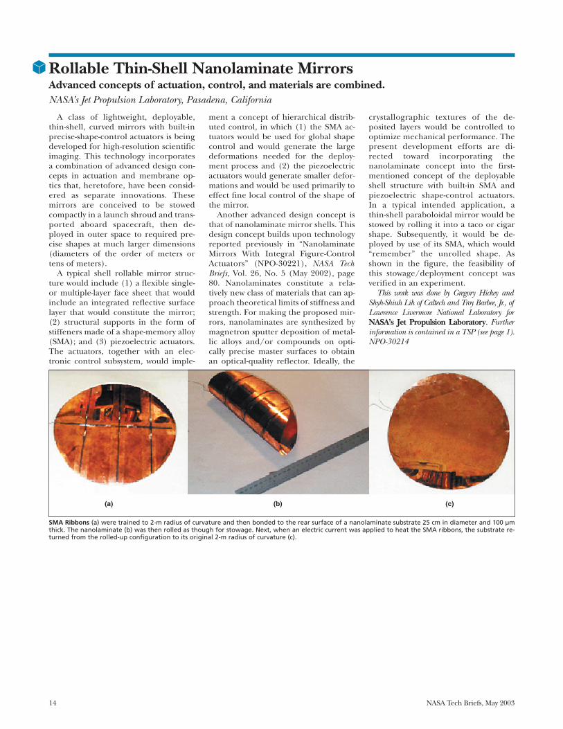
Rollable Thin-Shell Nanolaminate MirrorsAdvanced concepts of actuation, control, and materials are combined.NASA’s Jet Propulsion Laboratory, Pasadena, California
A class of lightweight, deployable,thin-shell, curved mirrors with built-inprecise-shape-control actuators is beingdeveloped for high-resolution scientificimaging. This technology incorporatesa combination of advanced design con-cepts in actuation and membrane op-tics that, heretofore, have been consid-ered as separate innovations. Thesemirrors are conceived to be stowedcompactly in a launch shroud and trans-ported aboard spacecraft, then de-ployed in outer space to required pre-cise shapes at much larger dimensions(diameters of the order of meters ortens of meters).
A typical shell rollable mirror struc-ture would include (1) a flexible single-or multiple-layer face sheet that wouldinclude an integrated reflective surfacelayer that would constitute the mirror;(2) structural supports in the form ofstiffeners made of a shape-memory alloy(SMA); and (3) piezoelectric actuators.The actuators, together with an elec-tronic control subsystem, would imple-
ment a concept of hierarchical distrib-uted control, in which (1) the SMA ac-tuators would be used for global shapecontrol and would generate the largedeformations needed for the deploy-ment process and (2) the piezoelectricactuators would generate smaller defor-mations and would be used primarily toeffect fine local control of the shape ofthe mirror.
Another advanced design concept isthat of nanolaminate mirror shells. Thisdesign concept builds upon technologyreported previously in “NanolaminateMirrors With Integral Figure-ControlActuators” (NPO-30221), NASA TechBriefs, Vol. 26, No. 5 (May 2002), page80. Nanolaminates constitute a rela-tively new class of materials that can ap-proach theoretical limits of stiffness andstrength. For making the proposed mir-rors, nanolaminates are synthesized bymagnetron sputter deposition of metal-lic alloys and/or compounds on opti-cally precise master surfaces to obtainan optical-quality reflector. Ideally, the
crystallographic textures of the de-posited layers would be controlled tooptimize mechanical performance. Thepresent development efforts are di-rected toward incorporating thenanolaminate concept into the first-mentioned concept of the deployableshell structure with built-in SMA andpiezoelectric shape-control actuators.In a typical intended application, athin-shell paraboloidal mirror would bestowed by rolling it into a taco or cigarshape. Subsequently, it would be de-ployed by use of its SMA, which would“remember” the unrolled shape. Asshown in the figure, the feasibility ofthis stowage/deployment concept wasverified in an experiment.
This work was done by Gregory Hickey andShyh-Shiuh Lih of Caltech and Troy Barbee, Jr., ofLawrence Livermore National Laboratory forNASA’s Jet Propulsion Laboratory. Furtherinformation is contained in a TSP (see page 1).NPO-30214
SMA Ribbons (a) were trained to 2-m radius of curvature and then bonded to the rear surface of a nanolaminate substrate 25 cm in diameter and 100 µmthick. The nanolaminate (b) was then rolled as though for stowage. Next, when an electric current was applied to heat the SMA ribbons, the substrate re-turned from the rolled-up configuration to its original 2-m radius of curvature (c).
(a) (b) (c)
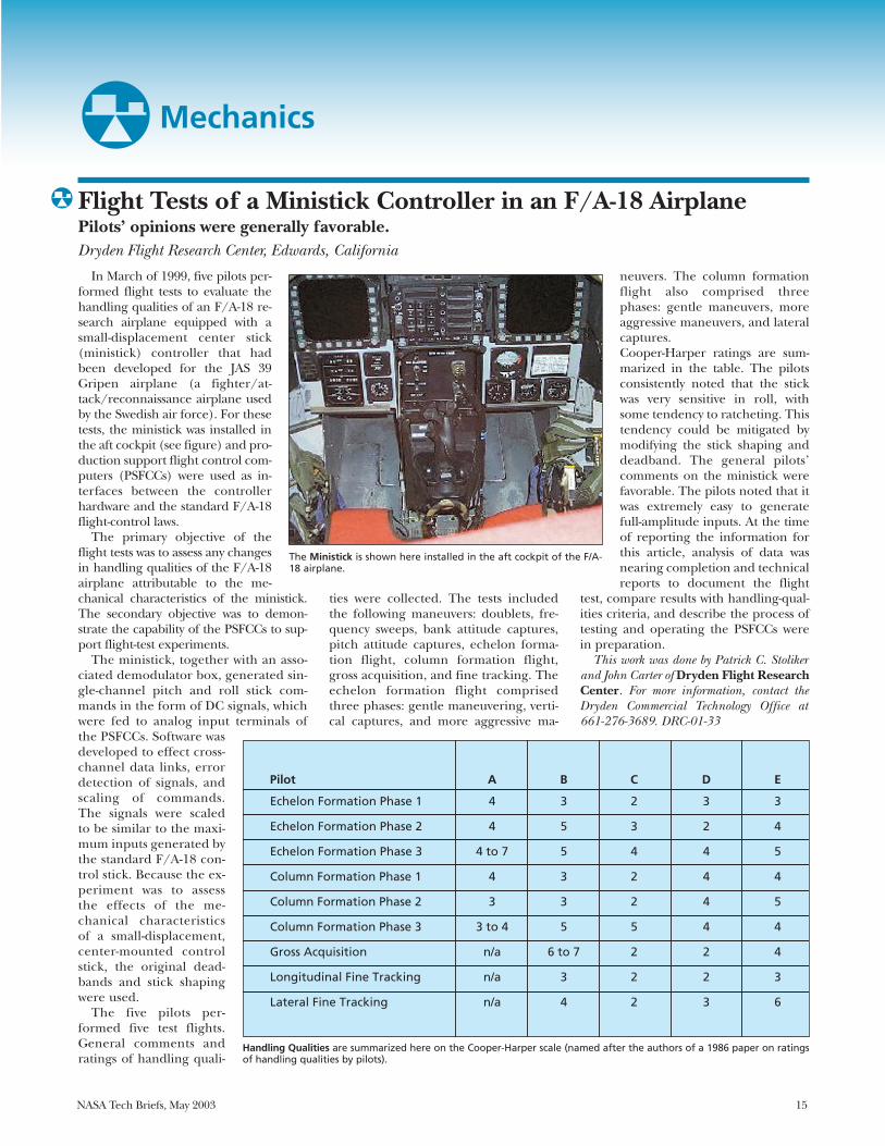
In March of 1999, five pilots per-formed flight tests to evaluate thehandling qualities of an F/A-18 re-search airplane equipped with asmall-displacement center stick(ministick) controller that hadbeen developed for the JAS 39Gripen airplane (a fighter/at-tack/reconnaissance airplane usedby the Swedish air force). For thesetests, the ministick was installed inthe aft cockpit (see figure) and pro-duction support flight control com-puters (PSFCCs) were used as in-terfaces between the controllerhardware and the standard F/A-18flight-control laws.
The primary objective of theflight tests was to assess any changesin handling qualities of the F/A-18airplane attributable to the me-chanical characteristics of the ministick.The secondary objective was to demon-strate the capability of the PSFCCs to sup-port flight-test experiments.
The ministick, together with an asso-ciated demodulator box, generated sin-gle-channel pitch and roll stick com-mands in the form of DC signals, whichwere fed to analog input terminals ofthe PSFCCs. Software wasdeveloped to effect cross-channel data links, errordetection of signals, andscaling of commands.The signals were scaledto be similar to the maxi-mum inputs generated bythe standard F/A-18 con-trol stick. Because the ex-periment was to assessthe effects of the me-chanical characteristicsof a small-displacement,center-mounted controlstick, the original dead-bands and stick shapingwere used.
The five pilots per-formed five test flights.General comments andratings of handling quali-
ties were collected. The tests includedthe following maneuvers: doublets, fre-quency sweeps, bank attitude captures,pitch attitude captures, echelon forma-tion flight, column formation flight,gross acquisition, and fine tracking. Theechelon formation flight comprisedthree phases: gentle maneuvering, verti-cal captures, and more aggressive ma-
neuvers. The column formationflight also comprised threephases: gentle maneuvers, moreaggressive maneuvers, and lateralcaptures.Cooper-Harper ratings are sum-marized in the table. The pilotsconsistently noted that the stickwas very sensitive in roll, withsome tendency to ratcheting. Thistendency could be mitigated bymodifying the stick shaping anddeadband. The general pilots’comments on the ministick werefavorable. The pilots noted that itwas extremely easy to generatefull-amplitude inputs. At the timeof reporting the information forthis article, analysis of data wasnearing completion and technicalreports to document the flight
test, compare results with handling-qual-ities criteria, and describe the process oftesting and operating the PSFCCs werein preparation.
This work was done by Patrick C. Stolikerand John Carter of Dryden Flight ResearchCenter. For more information, contact theDryden Commercial Technology Office at661-276-3689. DRC-01-33
NASA Tech Briefs, May 2003 15
Flight Tests of a Ministick Controller in an F/A-18 AirplanePilots’ opinions were generally favorable.Dryden Flight Research Center, Edwards, California
The Ministick is shown here installed in the aft cockpit of the F/A-18 airplane.
Handling Qualities are summarized here on the Cooper-Harper scale (named after the authors of a 1986 paper on ratingsof handling qualities by pilots).
Echelon Formation Phase 1
Pilot
Echelon Formation Phase 2
Echelon Formation Phase 3
Column Formation Phase 1
Column Formation Phase 2
Column Formation Phase 3
Gross Acquisition
Longitudinal Fine Tracking
Lateral Fine Tracking
2
C
3
4
2
2
5
2
2
2
3
D
2
4
4
4
4
2
2
3
3
E
4
5
4
5
4
4
3
6
3
B
5
5
3
3
5
6 to 7
3
4
4
A
4
4 to 7
4
3
3 to 4
n/a
n/a
n/a
Mechanics
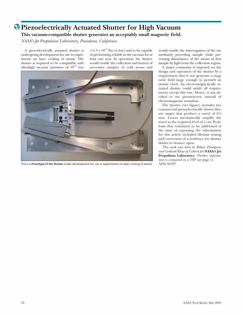
A piezoelectrically actuated shutter isundergoing development for use in exper-iments on laser cooling of atoms. Theshutter is required to be compatible withultrahigh vacuum [pressure of 10–9 torr
(≈1.3 × 10⁻⁷ Pa) or less] and to be capableof performing reliably in the vacuum for atleast one year. In operation, the shutterwould enable the collection and launch ofsuccessive samples of cold atoms and
would enable the interrogation of the im-mediately preceding sample while pre-venting disturbance of the atoms of thatsample by light from the collection region.
A major constraint is imposed on thedesign and operation of the shutter by arequirement that it not generate a mag-netic field large enough to perturb anatomic clock. An electromagnetically ac-tuated shutter could satisfy all require-ments except this one. Hence, it was de-cided to use piezoelectric instead ofelectromagnetic actuation.
The shutter (see figure) includes twocommercial piezoelectrically driven flex-ure stages that produce a travel of 0.5mm. Levers mechanically amplify thetravel to the required level of 1 cm. Prob-lems that remained to be addressed atthe time of reporting the informationfor this article included lifetime testingand correction of a tendency for shutterblades to bounce open.
This work was done by Robert Thompsonand Gerhard Klose of Caltech for NASA’s JetPropulsion Laboratory. Further informa-tion is contained in a TSP (see page 1).NPO-30397
16 NASA Tech Briefs, May 2003
This is a Prototype of the Shutter under development for use in experiments on laser cooling of atoms.
Piezoelectrically Actuated Shutter for High VacuumThis vacuum-compatible shutter generates an acceptably small magnetic field.NASA’s Jet Propulsion Laboratory, Pasadena, California

NASA Tech Briefs, May 2003 17
Machinery/Automation
Bio-Inspired Engineering of Exploration SystemsExploration systems with capabilities imbibed from nature enable new operations that wereotherwise very difficult or impossible to accomplish.NASA’s Jet Propulsion Laboratory, Pasadena, California
The multidisciplinary concept of“bioinspired engineering of explorationsystems” (BEES) is described, which is aguiding principle of the continuing ef-fort to develop biomorphic explorers asreported in a number of articles in thepast issues of NASA Tech Briefs. The intentof BEES is to distill from the principlesfound in successful nature-tested mecha-nisms of specific “crucial functions” thatare hard to accomplish by conventionalmethods but that are accomplishedrather deftly in nature by biological or-ganisms. The intent is not just to mimicoperational mechanisms found in a spe-cific biological organism but to imbibethe salient principles from a variety of di-verse bio-organisms for the desired “cru-cial function.” Thereby, we can build ex-plorer systems that have specificcapabilities endowed beyond nature, as
they will possess a combination of thebest nature-tested mechanisms for thatparticular function. The approach con-sists of selecting a crucial function, forexample, flight or some selected aspectsof flight, and develop an explorer thatcombines the principles of those specificattributes as seen in diverse flying speciesinto one artificial entity. This will allowgoing beyond biology and achieving un-precedented capability and adaptabilityneeded in encountering and exploringwhat is as yet unknown. A classificationof biomorphic flyers into two mainclasses of surface and aerial explorers isillustrated in the figure, with examplesof a variety of biological organisms thatprovide the inspiration in each respec-tive subclass.
Such biomorphic explorers may pos-sess varied mobility modes: surface-rov-
ing, burrowing, hopping, hovering, orflying, to accomplish surface, subsur-face, and aerial exploration. Prepro-grammed for a specific function, theycould serve as one-way communicatingbeacons, spread over the explorationsite, autonomously looking for/at thetargets of interest. In a hierarchical or-ganization, these biomorphic explorerswould report to the next level of explo-ration mode (say, a large conventionallander/rover) in the vicinity. A wide-spread and affordable exploration ofnew/hazardous sites at lower cost andrisk would thus become possible by uti-lizing a faster aerial flyer to cover longranges and deploying a variety of func-tion-specific, smaller biomorphic ex-plorers for distributed sensing andlocal sample acquisition. Several con-ceptual biomorphic missions for plane-
These Examples of Biological Inspirations show different mobility categories.
BiomorphicSubsurface Systems
BiomorphicSurface Systems
BiomorphicFlight Systems
Surface/SubsurfaceAerial
Biomorphic Explorers: Classification(Based on Mobility and Ambient Environment)
Biomorphic Explorers
Honeybee
Dragonfly Humming Bird
Monarch Butterfly
Inchworm
Ant
Centipede
Earthworm
GerminatingSeed
Seed Wing
Soaring Bird
18 NASA Tech Briefs, May 2003
tary and terrestrial exploration applica-tions have been illustrated in “Surface-Launched Explorers for Reconnais-sance/Scouting” (NPO-20871), NASATech Briefs, Vol. 26, No. 4 (April, 2002),page 69 and “Bio-Inspired Engineeringof Exploration Systems,” Journal ofSpace Mission Architecture, Issue 2, Fall2000, pages 49-79.
Insects (for example, honey bees anddragonflies) cope remarkably well withtheir world, despite possessing a brainthat carries less than 0.01 percent asmany neurons as that of the human. Al-though most insects have immobile eyes,fixed-focus optics, and lack stereo vision,they use a number of ingenious strate-gies for perceiving their world in threedimensions and navigating successfullyin it. We are distilling some of these in-sect-inspired strategies to obtain uniquesolutions to navigation, hazard avoid-ance, terrain following, and smooth de-ployment of payload. Such functionality
can enable one to reach previously un-reachable exploration sites.
In-situ, autonomous exploration andscience return from planetary surfacesand subsurfaces would be substantiallyenhanced if a large number of small, in-expensive, and therefore dispensable,biomorphic explorers equipped withdedicated microsensors could be spreadover the surface. Their low-cost andsmall size would make them ideal forhazardous or difficult site exploration,inspection, and testing. Their dedicatedsensing functions and autonomous ma-neuverability would be valuable in scout-ing missions and sample acquisitionfrom hard-to-reach places. As was men-tioned earlier, when preprogrammed fora specific function and spread over theexploration site, these explorers couldserve as intelligent, downlink-only bea-cons that autonomously look for objectsof interest. Alternatively, these biomor-phic explorers can operate in a hierar-
chical organization and report theirfindings to the next higher level of ex-ploration (say, a large conventional lan-der/rover) in the vicinity. Specifically,our recent results demonstrate the nov-elty of our approach in adapting princi-ples proven successful in nature toachieve stable flight control, navigation,and visual search/recognition. This ap-proach has enabled overall a robust ar-chitecture for reliable image data returnin application scenarios both for terres-trial and planetary needs where only alimited telecommunications or naviga-tional infrastructure is available and istherefore otherwise by traditional meth-ods hard or impossible to explore.
This work was done by Sarita Thakoor ofCaltech for NASA’s Jet Propulsion Labo-ratory. Further information is contained in aTSP (see page 1).NPO-21142

NASA Tech Briefs, May 2003 19
Manufacturing
Microscope Cells Containing Multiple Micromachined WellsThe cost per cell has been reduced substantially.John H. Glenn Research Center, Cleveland, Ohio
An improved design for multiple-wellmicroscope cells and an associated im-proved method of fabricating them havebeen devised. [As used here, “well” de-notes a cavity that has a volume of about1 or 2 µL and that is used to hold a sam-ple for examination under a micro-scope. As used here, “cell” denotes alaminate, based on a standard 1- by 3-in.(2.54- by 7.62-cm) microscope slide, thatcomprises (1) the slide as the lower layer,(2) an intermediate layer that containsholes that serve as the wells, and (3) atop layer that either consists of, or is sim-ilar to, a standard microscope-slide coverslip.] The improved design and methodof fabrication make it possible to in-crease (relative to a prior design andmethod of fabrication) the number ofwells per cell while reducing the fabrica-
tion loss and reducing the cost per cellto about one-tenth of the prior value.
In the prior design and method, theslide, well, and cover-slip layers weremade from silicate glass. The fabricationof each cell was a labor-intensive processthat included precise cutting and grind-ing of the glass components, fusing ofthe glass components, and then moregrinding and polishing to obtain desireddimensions. Cells of the prior designwere expensive and fragile, the rate ofloss in fabrication was high, and the na-ture of the glass made it difficult to in-crease the number of cells per well. Ef-forts to execute alternative prior designsin plastic have not yielded satisfactory re-sults because, for typical applications,plastics are not sufficiently thermally orchemically stable, not sufficiently opti-
cally clear, and/or not hard enough toresist scratching.
The figure depicts a cell of the presentimproved type. The slide and cover-sliplayers are made of a low-thermal-expansion glass (Pyrex™ or equivalent)and the intermediate (well layer) ismade of SiO2 — a combination of ma-terials that results in a laminatestronger than one made from layers ofsilicate glass. Before the layers are as-sembled into the laminate, the SiO2layer is micromachined to form thewells plus shallow grooves that, whensubsequently covered with the coverslip, become capillary channels that areused to fill the wells with samples. Themicromachining is accomplished byuse of the same patterning and etchingtechniques used to fabricate micro-electromechanical systems (MEMS).
Typically the thickness of the SiO2 layermust be made ≤200 µm — a requirementdictated by the viewing characteristics ofthe microscope and the nature of the mi-croscopic examination to be performed.Prior to assembly into the laminate, theslide and cover-slip layers should be opti-cally clear and should be polished to a tol-erance tight enough to enable electrosta-tic bonding to the well layer.
Once the cell has been assembled,each well is filled with a sample throughone of its capillary channels. Then an ul-traviolet-curing epoxy is wicked into allthe capillary channels, and the cell is ex-posed to ultraviolet light to cure theepoxy and thereby seal the samples intothe wells. The cell is then ready for ex-amination under a microscope.
This work was done by Walter Turnerand Robert Skupinski of Dynacs Engineer-ing Co., Inc., for Glenn Research Cen-ter. Further information is contained in a TSP(see page 1).
Inquiries concerning rights for the com-mercial use of this invention should be ad-dressed to NASA Glenn Research Center,Commercial Technology Office, Attn: SteveFedor, Mail Stop 4–8, 21000 BrookparkRoad, Cleveland, Ohio 44135. Refer toLEW-17016.
Low-Thermal-Expansion Glass Cover Slip
SiO2 Layer Containing Wells
Low-Thermal-Expansion Glass Microscope Slide
Low-Thermal-ExpansionGlass Cover Slip
SiO2 Layer Well
Capillary Channel
Low-Thermal-ExpansionGlass Microscope Slide
ASSEMBLED CELL
ENLARGED CROSS SECTION OF ONE WELL
Three Layers Are Electrostatically Bonded to produce a laminated multiple-well sample cell with cap-illary channels for filling the wells.
20 NASA Tech Briefs, May 2003
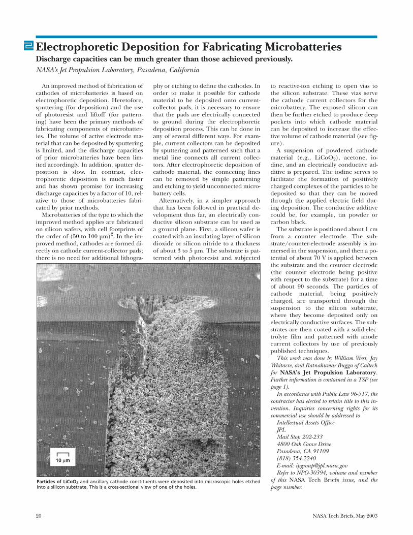
An improved method of fabrication ofcathodes of microbatteries is based onelectrophoretic deposition. Heretofore,sputtering (for deposition) and the useof photoresist and liftoff (for pattern-ing) have been the primary methods offabricating components of microbatter-ies. The volume of active electrode ma-terial that can be deposited by sputteringis limited, and the discharge capacitiesof prior microbatteries have been lim-ited accordingly. In addition, sputter de-position is slow. In contrast, elec-trophoretic deposition is much fasterand has shown promise for increasingdischarge capacities by a factor of 10, rel-ative to those of microbatteries fabri-cated by prior methods.
Microbatteries of the type to which theimproved method applies are fabricatedon silicon wafers, with cell footprints ofthe order of (50 to 100 µm)2. In the im-proved method, cathodes are formed di-rectly on cathode current-collector pads;there is no need for additional lithogra-
phy or etching to define the cathodes. Inorder to make it possible for cathodematerial to be deposited onto current-collector pads, it is necessary to ensurethat the pads are electrically connectedto ground during the electrophoreticdeposition process. This can be done inany of several different ways. For exam-ple, current collectors can be depositedby sputtering and patterned such that ametal line connects all current collec-tors. After electrophoretic deposition ofcathode material, the connecting linescan be removed by simple patterningand etching to yield unconnected micro-battery cells.
Alternatively, in a simpler approachthat has been followed in practical de-velopment thus far, an electrically con-ductive silicon substrate can be used asa ground plane. First, a silicon wafer iscoated with an insulating layer of silicondioxide or silicon nitride to a thicknessof about 3 to 5 µm. The substrate is pat-terned with photoresist and subjected
to reactive-ion etching to open vias tothe silicon substrate. These vias servethe cathode current collectors for themicrobattery. The exposed silicon canthen be further etched to produce deeppockets into which cathode materialcan be deposited to increase the effec-tive volume of cathode material (see fig-ure).
A suspension of powdered cathodematerial (e.g., LiCoO2), acetone, io-dine, and an electrically conductive ad-ditive is prepared. The iodine serves tofacilitate the formation of positivelycharged complexes of the particles to bedeposited so that they can be movedthrough the applied electric field dur-ing deposition. The conductive additivecould be, for example, tin powder orcarbon black.
The substrate is positioned about 1 cmfrom a counter electrode. The sub-strate/counter-electrode assembly is im-mersed in the suspension, and then a po-tential of about 70 V is applied betweenthe substrate and the counter electrode(the counter electrode being positivewith respect to the substrate) for a timeof about 90 seconds. The particles ofcathode material, being positivelycharged, are transported through thesuspension to the silicon substrate,where they become deposited only onelectrically conductive surfaces. The sub-strates are then coated with a solid-elec-trolyte film and patterned with anodecurrent collectors by use of previouslypublished techniques.
This work was done by William West, JayWhitacre, and Ratnakumar Bugga of Caltechfor NASA’s Jet Propulsion Laboratory.Further information is contained in a TSP (seepage 1).
In accordance with Public Law 96-517, thecontractor has elected to retain title to this in-vention. Inquiries concerning rights for itscommercial use should be addressed to
Intellectual Assets OfficeJPLMail Stop 202-2334800 Oak Grove DrivePasadena, CA 91109(818) 354-2240E-mail: [email protected] to NPO-30394, volume and number
of this NASA Tech Briefs issue, and thepage number.
Electrophoretic Deposition for Fabricating MicrobatteriesDischarge capacities can be much greater than those achieved previously.NASA’s Jet Propulsion Laboratory, Pasadena, California
Particles of LiCoO2 and ancillary cathode constituents were deposited into microscopic holes etchedinto a silicon substrate. This is a cross-sectional view of one of the holes.
10 µm
NASA Tech Briefs, May 2003 21
Physical Sciences
Integrated Arrays of Ion-Sensitive ElectrodesElectronic “tongues” would “taste” selected ions in water.NASA’s Jet Propulsion Laboratory, Pasadena, California
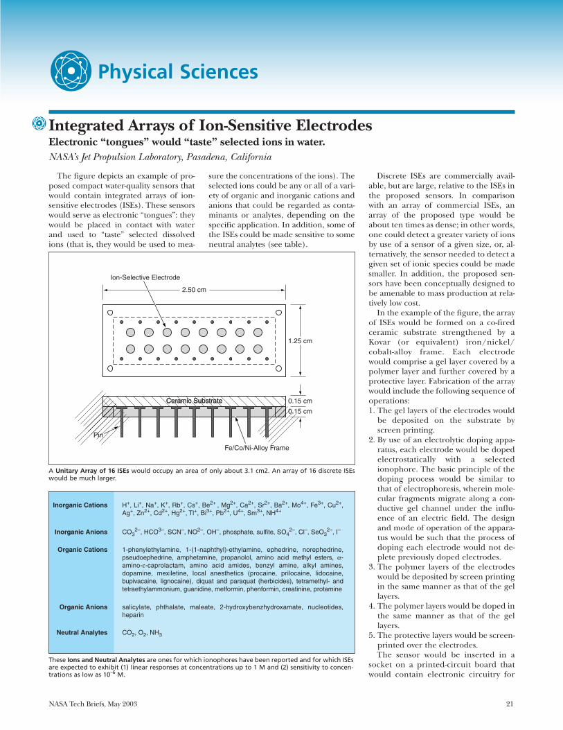
The figure depicts an example of pro-posed compact water-quality sensors thatwould contain integrated arrays of ion-sensitive electrodes (ISEs). These sensorswould serve as electronic “tongues”: theywould be placed in contact with waterand used to “taste” selected dissolvedions (that is, they would be used to mea-
sure the concentrations of the ions). Theselected ions could be any or all of a vari-ety of organic and inorganic cations andanions that could be regarded as conta-minants or analytes, depending on thespecific application. In addition, some ofthe ISEs could be made sensitive to someneutral analytes (see table).
Discrete ISEs are commercially avail-able, but are large, relative to the ISEs inthe proposed sensors. In comparisonwith an array of commercial ISEs, anarray of the proposed type would beabout ten times as dense; in other words,one could detect a greater variety of ionsby use of a sensor of a given size, or, al-ternatively, the sensor needed to detect agiven set of ionic species could be madesmaller. In addition, the proposed sen-sors have been conceptually designed tobe amenable to mass production at rela-tively low cost.
In the example of the figure, the arrayof ISEs would be formed on a co-firedceramic substrate strengthened by aKovar (or equivalent) iron/nickel/cobalt-alloy frame. Each electrodewould comprise a gel layer covered by apolymer layer and further covered by aprotective layer. Fabrication of the arraywould include the following sequence ofoperations:1. The gel layers of the electrodes would
be deposited on the substrate byscreen printing.
2. By use of an electrolytic doping appa-ratus, each electrode would be dopedelectrostatically with a selectedionophore. The basic principle of thedoping process would be similar tothat of electrophoresis, wherein mole-cular fragments migrate along a con-ductive gel channel under the influ-ence of an electric field. The designand mode of operation of the appara-tus would be such that the process ofdoping each electrode would not de-plete previously doped electrodes.
3. The polymer layers of the electrodeswould be deposited by screen printingin the same manner as that of the gellayers.
4. The polymer layers would be doped inthe same manner as that of the gellayers.
5. The protective layers would be screen-printed over the electrodes.The sensor would be inserted in a
socket on a printed-circuit board thatwould contain electronic circuitry for
A Unitary Array of 16 ISEs would occupy an area of only about 3.1 cm2. An array of 16 discrete ISEswould be much larger.
0.15 cm
1.25 cm
2.50 cm
Ceramic SubstrateCeramic Substrate
Ion-Selective Electrode
Fe/Co/Ni-Alloy Frame
Pin
0.15 cm
These Ions and Neutral Analytes are ones for which ionophores have been reported and for which ISEsare expected to exhibit (1) linear responses at concentrations up to 1 M and (2) sensitivity to concen-trations as low as 10–6 M.
Inorganic Cations H+, Li+, Na+, K+, Rb+, Cs+, Be2+ , Mg2+, Ca2+, Sr2+, Ba2+, Mo4+, Fe3+, Cu2+, Ag+, Zn2+, Cd2+, Hg2+, Tl+, Bi3+, Pb2+, U4+, Sm3+, NH4+
Inorganic Anions CO32–, HCO3–, SCN–, NO2–, OH–, phosphate, sulfite, SO4
2–, Cl–, SeO32–, I–
Organic Cations 1-phenylethylamine, 1-(1-naphthyl)-ethylamine, ephedrine, norephedrine, pseudoephedrine, amphetamine, propanolol, amino acid methyl esters, α-amino-ε-caprolactam, amino acid amides, benzyl amine, alkyl amines, dopamine, mexiletine, local anesthetics (procaine, prilocaine, lidocaine, bupivacaine, lignocaine), diquat and paraquat (herbicides), tetramethyl- and tetraethylammonium, guanidine, metformin, phenformin, creatinine, protamine
Organic Anions salicylate, phthalate, maleate, 2-hydroxybenzhydroxamate, nucleotides, heparin
Neutral Analytes CO2, O2, NH3

22 NASA Tech Briefs, May 2003
processing the ISE outputs. The cir-cuitry would include analog-to-digitalconverters measuring the ISE poten-tials. The circuitry would also includedigital multiplexers for transmittingthe potentials to a computer, whichwould analyze the potentials to deter-mine the concentrations of ions of theselected species.
This work was done by Martin Buehlerand Kimberly Kuhlman of Caltech forNASA’s Jet Propulsion Laboratory. Fur-ther information is contained in a TSP (seepage 1).
In accordance with Public Law 96-517, thecontractor has elected to retain title to this in-vention. Inquiries concerning rights for itscommercial use should be addressed to
Intellectual Property groupJPLMail Stop 202-2334800 Oak Grove DrivePasadena, CA 91109(818) 354-2240Refer to NPO-20700, volume and number
of this NASA Tech Briefs issue, and thepage number.
Model of Fluidized Bed Containing Reacting Solids and GasesThis model can be used to optimize designs and operating conditions.NASA’s Jet Propulsion Laboratory, Pasadena, California
A mathematical model has been devel-oped for describing the thermofluid dy-namics of a dense, chemically reactingmixture of solid particles and gases. Asused here, “dense” signifies having alarge volume fraction of particles, as forexample in a bubbling fluidized bed. Themodel is intended especially for applica-tion to fluidized beds that contain mix-tures of carrier gases, biomass undergo-ing pyrolysis, and sand. So far, the designof fluidized beds and other gas/solid in-dustrial processing equipment has beenbased on empirical correlations derivedfrom laboratory- and pilot-scale units.The present mathematical model is aproduct of continuing efforts to develop
a computational capability for optimiz-ing the designs of fluidized beds and re-lated equipment on the basis of first prin-ciples. Such a capability could eliminatethe need for expensive, time-consumingpredesign testing.
The present model includes compo-nents in common with models describedin several previous NASA Tech Briefs arti-cles, including, most notably, “Model ofPyrolysis of Biomass in a Fluidized-BedReactor” (NPO-20708), NASA Tech Briefs,Vol. 25, No. 6 (June 2001), page 59;“Multiphase-Flow Model of Fluidized-Bed Pyrolysis of Biomass” (NPO-20789),NASA Tech Briefs, Vol. 26, No. 2 (Febru-ary 2002), page 56; and “Model of a Flu-
idized Bed Containing a Mixture of Par-ticles” (NPO-20937), NASA Tech Briefs,Vol. 26, No. 4 (April 2002), page 56. Themodel distinguishes among multipleparticle classes on the basis of physicalproperties (e.g., diameter or density)and/or through thermochemical prop-erties (e.g., chemical reactivity or nonre-activity). The formulation of the modelfollows a multifluid approach in whichmacroscopic equations for the solidphase are derived from a kinetic-like the-ory considering inelastic-rigid-spheresubmodels in accounting for collisionaltransfer in high-density regions. The gasphase equations are derived using en-semble averaging.
Separate transport equations are con-structed for each of the particle classes,providing for the separate description ofthe acceleration of the particles in eachclass, of interactions between particles indifferent size classes, and of the equili-bration processes in which momentumand energy are exchanged among theparticle classes and the carrier gas. Thekinetic-like theory is based on a Gaussianapproximation of the velocity distribu-tion, assuming that spatial gradients ofmean variables are small and particlesare nearly elastic. Each class of particlesis characterized by its own granular tem-perature, which represents the mean ki-netic energy associated with fluctuationsin the velocities of the particles. Thestress tensor is augmented by a frictional-transfer submodel of stress versus strain:The separate equations of the dynamicsof the various particle classes are cou-pled through source terms that describesuch nonequilibrium processes as trans-fer of mass, momentum, and energy,both between particles and between gasand particles.
In one of several test cases, the modelwas applied to the pyrolysis of biomass
The Tar Yield of a Fluidized Bed as a function of time was computed, for various temperatures of flu-idizing gas, by use of the model described in the text.
800 K
750 K
850 K
700 K
950 K
600 K
00
0.1
0.2
0.3
0.4
0.5
0.6
1 2
Time, Seconds
3 4 5
Tar Y
ield
NASA Tech Briefs, May 2003 23
particles in a laboratory fluidized bed re-actor and used to compute yields of re-action products (especially tar). The re-sults indicate that at fixed initial particlesize, the temperature of the fluidizinggas is the foremost parameter that influ-
ences the tar yield and can be chosen tomaximize the tar yield (see figure). Thetemperature of the biomass feed, the na-ture of the feedstock, and the fluidiza-tion velocity were all found to exert onlyminor effects on the tar yield.
This work was done by Josette Bellanand Danny Lathouwers of Caltech forNASA’s Jet Propulsion Laboratory.Further information is contained in a TSP (seepage 1).NPO-30163
Membrane Mirrors With Bimorph Shape ActuatorsOnly modest control voltages would be needed.NASA’s Jet Propulsion Laboratory, Pasadena, California
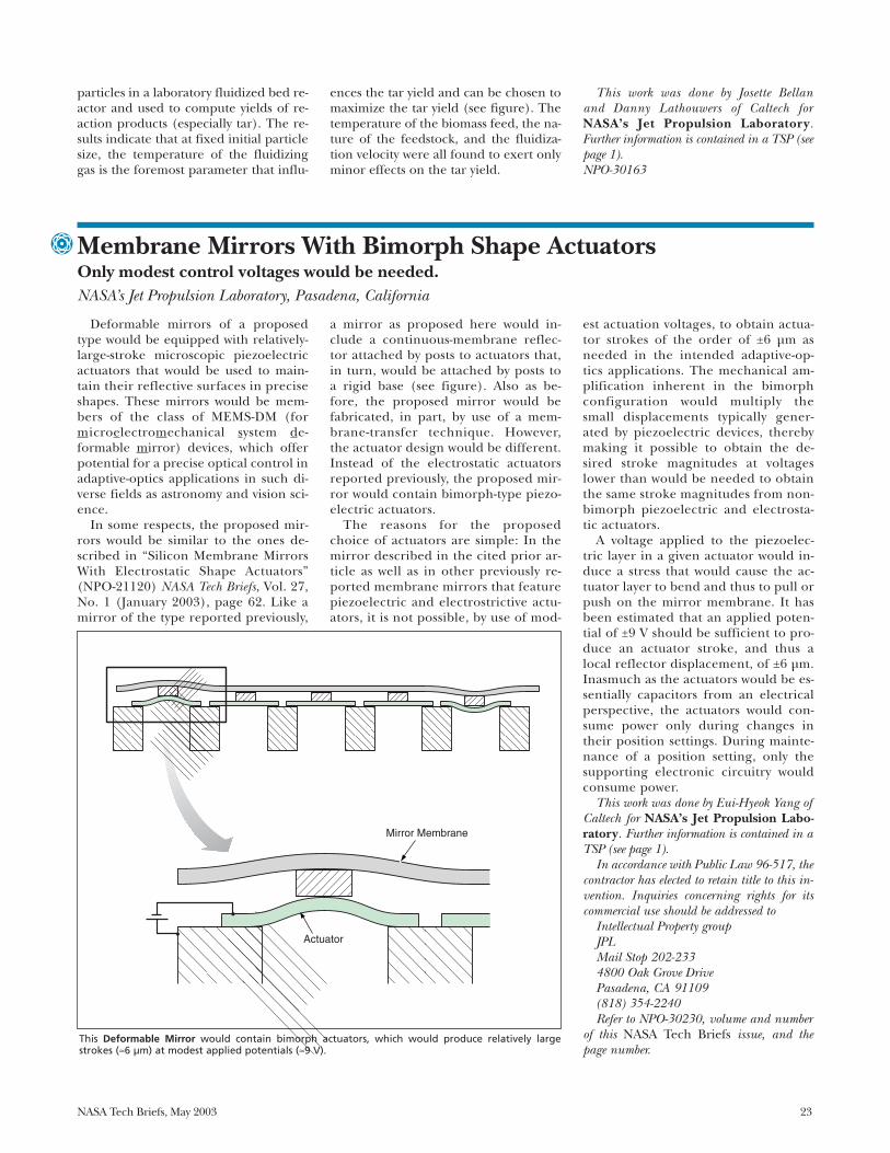
Deformable mirrors of a proposedtype would be equipped with relatively-large-stroke microscopic piezoelectricactuators that would be used to main-tain their reflective surfaces in preciseshapes. These mirrors would be mem-bers of the class of MEMS-DM (formicroelectromechanical system de-formable mirror) devices, which offerpotential for a precise optical control inadaptive-optics applications in such di-verse fields as astronomy and vision sci-ence.
In some respects, the proposed mir-rors would be similar to the ones de-scribed in “Silicon Membrane MirrorsWith Electrostatic Shape Actuators”(NPO-21120) NASA Tech Briefs, Vol. 27,No. 1 (January 2003), page 62. Like amirror of the type reported previously,
a mirror as proposed here would in-clude a continuous-membrane reflec-tor attached by posts to actuators that,in turn, would be attached by posts toa rigid base (see figure). Also as be-fore, the proposed mirror would befabricated, in part, by use of a mem-brane-transfer technique. However,the actuator design would be different.Instead of the electrostatic actuatorsreported previously, the proposed mir-ror would contain bimorph-type piezo-electric actuators.
The reasons for the proposedchoice of actuators are simple: In themirror described in the cited prior ar-ticle as well as in other previously re-ported membrane mirrors that featurepiezoelectric and electrostrictive actu-ators, it is not possible, by use of mod-
est actuation voltages, to obtain actua-tor strokes of the order of ±6 µm asneeded in the intended adaptive-op-tics applications. The mechanical am-plification inherent in the bimorphconfiguration would multiply thesmall displacements typically gener-ated by piezoelectric devices, therebymaking it possible to obtain the de-sired stroke magnitudes at voltageslower than would be needed to obtainthe same stroke magnitudes from non-bimorph piezoelectric and electrosta-tic actuators.
A voltage applied to the piezoelec-tric layer in a given actuator would in-duce a stress that would cause the ac-tuator layer to bend and thus to pull orpush on the mirror membrane. It hasbeen estimated that an applied poten-tial of ±9 V should be sufficient to pro-duce an actuator stroke, and thus alocal reflector displacement, of ±6 µm.Inasmuch as the actuators would be es-sentially capacitors from an electricalperspective, the actuators would con-sume power only during changes intheir position settings. During mainte-nance of a position setting, only thesupporting electronic circuitry wouldconsume power.
This work was done by Eui-Hyeok Yang ofCaltech for NASA’s Jet Propulsion Labo-ratory. Further information is contained in aTSP (see page 1).
In accordance with Public Law 96-517, thecontractor has elected to retain title to this in-vention. Inquiries concerning rights for itscommercial use should be addressed to
Intellectual Property groupJPLMail Stop 202-2334800 Oak Grove DrivePasadena, CA 91109(818) 354-2240Refer to NPO-30230, volume and number
of this NASA Tech Briefs issue, and thepage number.
This Deformable Mirror would contain bimorph actuators, which would produce relatively largestrokes (≈6 µm) at modest applied potentials (≈9 V).
Actuator
Mirror Membrane

NASA Tech Briefs, May 2003 25
Information Sciences
Using Fractional Clock-Period Delays in Telemetry ArrayingSpecial digital FIR filters help to increase accuracy.NASA’s Jet Propulsion Laboratory, Pasadena, California
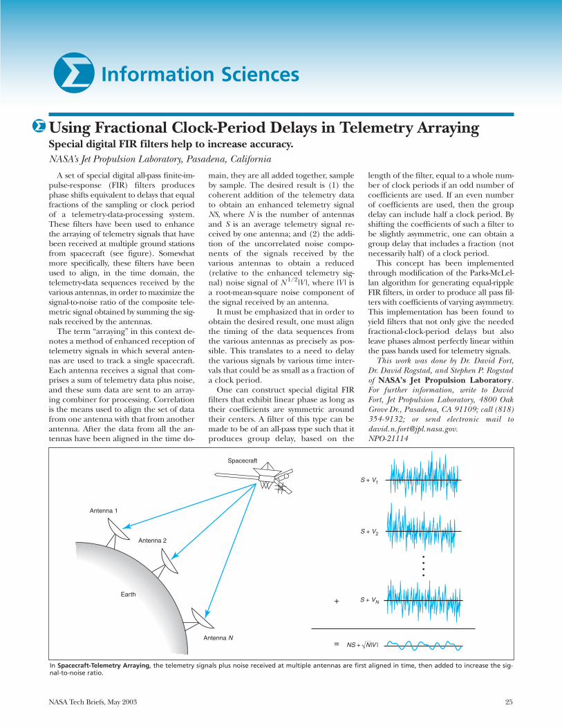
A set of special digital all-pass finite-im-pulse-response (FIR) filters producesphase shifts equivalent to delays that equalfractions of the sampling or clock periodof a telemetry-data-processing system.These filters have been used to enhancethe arraying of telemetry signals that havebeen received at multiple ground stationsfrom spacecraft (see figure). Somewhatmore specifically, these filters have beenused to align, in the time domain, thetelemetry-data sequences received by thevarious antennas, in order to maximize thesignal-to-noise ratio of the composite tele-metric signal obtained by summing the sig-nals received by the antennas.
The term “arraying” in this context de-notes a method of enhanced reception oftelemetry signals in which several anten-nas are used to track a single spacecraft.Each antenna receives a signal that com-prises a sum of telemetry data plus noise,and these sum data are sent to an array-ing combiner for processing. Correlationis the means used to align the set of datafrom one antenna with that from anotherantenna. After the data from all the an-tennas have been aligned in the time do-
main, they are all added together, sampleby sample. The desired result is (1) thecoherent addition of the telemetry datato obtain an enhanced telemetry signalNS, where N is the number of antennasand S is an average telemetry signal re-ceived by one antenna; and (2) the addi-tion of the uncorrelated noise compo-nents of the signals received by thevarious antennas to obtain a reduced(relative to the enhanced telemetry sig-nal) noise signal of N 1/2|V |, where |V | isa root-mean-square noise component ofthe signal received by an antenna.
It must be emphasized that in order toobtain the desired result, one must alignthe timing of the data sequences fromthe various antennas as precisely as pos-sible. This translates to a need to delaythe various signals by various time inter-vals that could be as small as a fraction ofa clock period.
One can construct special digital FIRfilters that exhibit linear phase as long astheir coefficients are symmetric aroundtheir centers. A filter of this type can bemade to be of an all-pass type such that itproduces group delay, based on the
length of the filter, equal to a whole num-ber of clock periods if an odd number ofcoefficients are used. If an even numberof coefficients are used, then the groupdelay can include half a clock period. Byshifting the coefficients of such a filter tobe slightly asymmetric, one can obtain agroup delay that includes a fraction (notnecessarily half) of a clock period.
This concept has been implementedthrough modification of the Parks-McLel-lan algorithm for generating equal-rippleFIR filters, in order to produce all pass fil-ters with coefficients of varying asymmetry.This implementation has been found toyield filters that not only give the neededfractional-clock-period delays but alsoleave phases almost perfectly linear withinthe pass bands used for telemetry signals.
This work was done by Dr. David Fort,Dr. David Rogstad, and Stephen P. Rogstadof NASA’s Jet Propulsion Laboratory.For further information, write to DavidFort, Jet Propulsion Laboratory, 4800 OakGrove Dr., Pasadena, CA 91109; call (818)354-9132; or send electronic mail [email protected]
In Spacecraft-Telemetry Arraying, the telemetry signals plus noise received at multiple antennas are first aligned in time, then added to increase the sig-nal-to-noise ratio.
Antenna 1
Antenna 2
Earth
Antenna N
Spacecraft
S + V1
S + V2
S + VN
NS + N|V |
+
=
26 NASA Tech Briefs, May 2003
A proposed approach to the develop-ment of software for spacecraft avionicsis based partly on a concept of genericsoftware that could be tailored to satisfyrequirements for specific missions. Theproposed approach would stand in con-trast to the conventional approach offirst defining avionics requirements fora specific mission, then developing soft-ware specific to those requirements.The proposed approach might also beadaptable to programming computersthat control and monitor other com-plex equipment systems that range inscale from automobiles to factories.
The concept of a spacecraft avionicsfunctional model (SAFM) is a majorelement of the proposed approach. AnSAFM would be, essentially, a system-atic and hierarchical description ofthe functionality required of theavionics software (and hardware) for agiven mission. Although the initialinput information used to start theconstruction of an SAFM would typi-cally amount to a high-level descrip-tion, the SAFM would thereafter bedecomposed to a low level. The result-ing low-level version of the modelwould be used to develop a set ofgeneric requirements that could beexpected to include a large fraction ofall requirements for a large fraction ofall missions. The generic require-ments would be used to develop soft-ware modules that could be includedin, or excluded from, the final flightsoftware to satisfy the requirements ofa specific mission.
By creating the opportunity to reusecommon software modules on differentmissions, this approach would reducethe time, cost, and difficulty of develop-ing the software. In addition, a high de-gree of reuse is expected to lead to in-creased reliability.
An SAFM would lend itself to any orall of the following five applications:• Education and Training
The standard breakdown of function-ality would be helpful in educationand professional training in the func-tions that occur aboard a typicalspacecraft.
• Systems EngineeringThe breakdown would proceed,more specifically, from functions tosubfunctions to roles. Such a break-down would bring a standard tem-plate to part of the documentation ofrequirements. A standard templateof this nature would increase the ef-ficiency and enhance the utility ofsoftware tools used to document therequirements, while remaining flexi-ble enough to be useful for a numberof different projects. The standardtemplate would, in effect, be a tex-tual version of the hierarchy of theSAFM, placed into the functional-re-quirements portion of the require-ments documentation for the space-craft in question.A key element of this approach is that
at the breakdown-of-requirements stageof development of a given system, therequirements would be documentedwith respect to functionality but wouldnot yet have been allocated to specificsubsystems. It would still be possible, atthis stage, to develop any of a numberof different avionics architectures thatwould satisfy all the documented re-quirements.• Modeling of Resources
The next step would be the estima-tion of the avionics resources used byeach of the roles, and of how theseavionics resources change withchanges in the requirements of theroles. The next step would be to tab-ulate the resources required for eachrole, and then for each subfunction,in order to determine the resourcesused by each function. Once func-tions were assigned to subsystems, itwould then be possible to determinethe resources required by each sub-system.
• Analysis, Tradeoffs, and Estimation of CostsIf the modeling as described thus farwere to be implemented with thehelp of an automated or semiauto-mated software tool, the next stepwould be to model a number of ar-chitectures and functional break-downs. The architectures would dif-fer in the functions assigned to
different hardware subsystems. Thismodeling would yield estimates ofsuch parameters as memory usage,data and processor instruction rates,bus bandwidth, power usage, mass,and volume. These estimates couldbe used to determine which of theproposed architectures would bestsatisfy mission requirements, whichwould be most flexible, and how thedifferent architectures would use sys-tem resources. The final step in mod-eling would be to estimate the costsof the candidate avionics architec-tures.
• Functional Standardization and Common-alityIn an SAFM, the relationships amongthe roles within a subfunction wouldbe the same. In other words, theroles would have constant functionalcontents, and their inputs and out-puts would stay constant, or nearlyso. This implies that if a role wereused in more than one mission, itmay be possible to reuse, from onespacecraft to another, the softwaremodule that implements that role. Ifthis were done for a few missions, a li-brary of software modules wouldsoon be built up, making it possiblefor the next mission to limit itself todeveloping code for only those cor-responding functional modules thatwere new, that were characterized bysignificantly different requirements,or that had grown antiquated.This work was done by Joseph Smith of Cal-
tech for NASA’s Jet Propulsion Labora-tory. Further information is contained in aTSP (see page 1).
In accordance with Public Law 96-517, thecontractor has elected to retain title to this in-vention. Inquiries concerning rights for itscommercial use should be addressed to
Intellectual Property groupJPLMail Stop 202-2334800 Oak Grove DrivePasadena, CA 91109(818) 354-2240Refer to NPO-20968, volume and number
of this NASA Tech Briefs issue, and thepage number.
Developing Generic Software for Spacecraft AvionicsA standardized functional model would facilitate cost-effective reuse of common software modules.NASA’s Jet Propulsion Laboratory, Pasadena, California
NASA Tech Briefs, May 2003 27
Numerical Study of Pyrolysis of Biomass in Fluidized Beds
A report presents a numerical-simu-lation study of pyrolysis of biomass influidized-bed reactors, performed byuse of the mathematical model de-scribed in “Model of Fluidized BedContaining Reacting Solids and Gases”(NPO-30163), which appears else-where in this issue of NASA Tech Briefs.The purpose of the study was to inves-tigate the effect of various operatingconditions on the efficiency of pro-duction of condensable tar from bio-mass. The numerical results indicatethat for a fixed particle size, the flu-idizing-gas temperature is the fore-most parameter that affects the taryield. For the range of fluidizing-gastemperatures investigated, and underthe assumption that the pyrolysis rateexceeds the feed rate, the optimumsteady-state tar collection was found tooccur at 750 K. In cases in which theassumption was not valid, the opti-mum temperature for tar collectionwas found to be only slightly higher.Scaling up of the reactor was found toexert a small negative effect on tar col-lection at the optimal operating tem-perature. It is also found that slightlybetter scaling is obtained by use ofshallower fluidized beds with greaterfluidization velocities.
This work was done by Josette Bellanand Danny Lathouwers of Caltech forNASA’s Jet Propulsion Laboratory.Further information is contained in a TSP (seepage 1).NPO-30164
Assessment of Models ofChemically Reacting Granular Flows
A report presents an assessment of ageneral mathematical model of dense,chemically reacting granular flows likethose in fluidized beds used to py-rolize biomass. The model incorpo-rates submodels that have been de-scribed in several NASA Tech Briefsarticles, including “GeneralizedMathematical Model of Pyrolysis ofBiomass” (NPO-20068) NASA TechBriefs, Vol. 22, No. 2 (February 1998),page 60; “Model of Pyrolysis of Bio-mass in a Fluidized-Bed Reactor”(NPO-20708), NASA Tech Briefs, Vol.25, No. 6 (June 2001), page 59; and“Model of Fluidized Bed ContainingReacting Solids and Gases” (NPO-30163), which appears elsewhere inthis issue. The model was used to per-form computational simulations in atest case of pyrolysis in a reactor con-taining sand and biomass (i.e., plantmaterial) particles through whichpasses a flow of hot nitrogen. Theboundary conditions and other param-eters were selected for the test case toenable assessment of the validity ofsome assumptions incorporated intosubmodels of granular stresses, granu-lar thermal conductivity, and heatingof particles. The results of the simula-tion are interpreted as partly affirmingthe assumptions in some respects andindicating the need for refinements ofthe assumptions and the affected sub-models in other respects.
This work was done by Josette Bellanand Danny Lathouwers of Caltech forNASA’s Jet Propulsion Laboratory.Further information is contained in a TSP (seepage 1).NPO-30264
Books & Reports


National Aeronautoics andSpace Adninistration