Embed Size (px)
Citation preview

Technical University of Crete
School of Electrical & Computer Engineering
Implementation of an ARM Processor
with SIMD Extensions using the Bluespec
Hardware Description Language
by
Makrygiannis Konstantinos
Thesis Committee
Professor Pnevmatikatos Dionisios (Supervisor) (ECE)
Professor Dollas Apostolos (ECE)
Dr. Theodoropoulos Dimitrios (ECE)
Chania, May 2018


i | Acknowledgements
Acknowledgements
First, I would like to thank my supervisor, Professor Dionisios Pnevmatikatos
for his guidance and support, as well as for the opportunity to work on innovative tech-
nology development, knowing that my work will be used for further advances in the
field. This thesis would not be possible without his help and patience.
I would also like to express my gratitude to Prof. Apostolos Dollas and Dr. Di-
mitrios Theodoropoulos for their interest in my work and for contributing to its evalu-
ation as members of the thesis committee.
In addition, I would like to thank my girlfriend for her love and support all these
years.
Last and most important, I would like to thank my parents for their huge support
over the years. This thesis is dedicated to them.

ii | Abstract
Abstract
The goal of this thesis was to implement an ARM processor with Single Instruc-
tion Multiple Data (SIMD) extensions using the Bluespec System Verilog (BSV) as a
Hardware Description Language (HDL). BSV has a fundamentally different approach
to hardware design, comparing to other HDLs. It is based on circuit generation - rather
than merely circuit description - and on atomic transactional rules instead of a globally
synchronous view of the world. BSV language is considered a high-level functional
HDL, which was essentially Haskell - extended to handle chip design and electronic
design automation in general. BSV is partially evaluated (to convert the Haskell parts)
and compiled to the Term Rewriting System (TRS). Our scalar processor supports a 3-
stage pipeline (Fetch – Decode – Execute), belongs to the ARM7 family and uses a 32-
bit architecture, which is based on ARMv4 instruction set. The SIMD unit works as an
extension to the scalar part and is based on a modification of ARM NEON technology.
The scalar part of the processor supports Data processing, Multiply, Long Multiply,
Load/Store – Byte/Word and Branch instructions of the ARM Instruction Set Format,
while the vector part supports Vector Data Processing, Vector Multiply and Vector
Load/Store instructions.

iii |

iv | Contents
Contents Acknowledgements ....................................................................................................... i
Abstract ......................................................................................................................... ii
1. Introduction .............................................................................................................. 1
2. Bluespec System Verilog.......................................................................................... 2
2.1 Bluespec Syntax ................................................................................................. 3
2.2 Types in Bluespec ............................................................................................ 4
2.3 The Bluespec Compiler................................................................................... 6
2.3.1 Scheduling ................................................................................................... 7
2.3.2 The Bluesim Simulator .............................................................................. 8
3. ARM Scalar Unit...................................................................................................... 9
3.1 ARM Architecture ........................................................................................ 10
3.1.1 ARM Processor Modes ............................................................................ 10
3.1.2 ARM Registers ......................................................................................... 11
3.2 ARM v4 Instruction Set Architecture ......................................................... 13
3.2.1 Conditional Execution ............................................................................. 14
3.2.2 Shifts & Rotates........................................................................................ 14
3.2.3 Branch and Branch with Link (B, BL) .................................................. 15
3.2.4 Data Processing ........................................................................................ 15
3.2.5 Multiply and Multiply-Accumulate (MUL, MLA) ............................... 18
3.2.6 Multiply Long and Multiply-Accumulate Long (MULL, MLAL) ...... 18
3.2.7 Single Data Transfer (LDR, STR) .......................................................... 19
4. ARM Vector Unit ................................................................................................... 22
4.1 Comparing Scalar to Vector ........................................................................ 23
4.2 Vector Architecture ...................................................................................... 24
4.2.1 Components of a Vector Processor ........................................................ 24
4.2.2 Advantages of Vector Instruction Set Architecture ............................. 24
4.3 Our Vector Instruction Set Architecture .................................................... 25
4.3.1 Vector Data Processing............................................................................ 26
4.3.2 Vector Multiply and Vector Multiply-Accumulate (VMUL, VMLA) 29
4.3.3 Vector Load and Vector Store (VLD, VST) .......................................... 30

v | Contents
5. Implementation ...................................................................................................... 33
5.1 Scalar Implementation ................................................................................. 34
5.1.1 Instruction Memory Module ................................................................... 34
5.1.2 Decode Module ......................................................................................... 35
5.1.3 Barrel Shifter Module.............................................................................. 36
5.1.4 ALU Module ............................................................................................. 36
5.1.5 Multiplier Module .................................................................................... 38
5.1.6 Register File Module ................................................................................ 39
5.1.7 Data Memory Module.............................................................................. 40
5.2 Vector Implementation ................................................................................. 40
5.2.1 Vector Barrel Shifter Module ................................................................. 41
5.2.2 Vector ALU Module ................................................................................ 41
5.2.3 Vector Multiplier Module ....................................................................... 41
5.2.4 Vector Register File Module ................................................................... 42
5.2.5 Vector Data Memory Module ................................................................. 46
5.3 Testbench Module – Top Module ................................................................ 46
6. Debugging and Testing .......................................................................................... 49
6.1 Debugging of the Design ............................................................................... 49
6.2 Testing the Scalar Unit ................................................................................. 51
6.2.1 “By-hand” Testing Example ................................................................... 52
6.2.2 Factorial Testing Example ...................................................................... 53
6.2.3 Largest Number Among Three (LNA3) Testing Example ................... 54
6.2.4 Fibonacci Testing Example ..................................................................... 56
6.2.5 Bubblesort Testing Example ................................................................... 58
6.3 Testing the Vector Unit ................................................................................ 60
6.3.1 Parallelization Example........................................................................... 61
6.3.2 Vector Multiply Example ........................................................................ 61
6.3.3 Vector Load and Vector Store Example ................................................ 63
6.3.4 Multiple Scalar & Vector Instructions Example .................................. 64
6.4 Design Evaluation ......................................................................................... 65
7. Conclusion .............................................................................................................. 67
7.1 Conclusion of Thesis ........................................................................................ 67
7.2 Future Work ..................................................................................................... 67
Bibliography ............................................................................................................... 68

vi | List of Figures
List of Figures
Figure 2. 1: A Bluespec's Standard Module ............................................................................... 4
Figure 2. 2: Bluespec's Data Type conversion functions ........................................................... 6
Figure 2. 3: Bluespec's Compiler Design Flow ........................................................................... 7
Figure 3. 1: Arm Register Set ................................................................................................... 11
Figure 3. 2: Current Program Status Register Format ............................................................. 12
Figure 3. 3: ARM Instruction Set Format ................................................................................. 13
Figure 3. 4: Condition Codes & Conditional Execution ............................................................ 14
Figure 3. 5: ARM Branch Instructions Encoding ...................................................................... 15
Figure 3. 6: ARM Data Processing Instructions ....................................................................... 15
Figure 3. 7: ARM Data Processing Instructions Encoding ........................................................ 16
Figure 3. 8: ARM Shift Operations Encoding ........................................................................... 17
Figure 3. 9: ARM Multiply Instructions Encoding .................................................................... 18
Figure 3. 10: ARM Multiply Long Instructions Encoding ......................................................... 18
Figure 3. 11: ARM Single Data Transfer Instructions Encoding ............................................... 19
Figure 3. 12: ARM Theoretical Datapath ................................................................................. 21
Figure 4. 1: A typical Vector Processing Unit ........................................................................... 22
Figure 4. 2: (A): A 64-bit scalar register, and (B): A vector register of 8 64-bit elements ....... 23
Figure 4. 3: Difference between scalar and vector add instructions ...................................... 23
Figure 4. 4: Our Vector Instruction Set Format ....................................................................... 25
Figure 4. 5: Vector Add (VADD) Instruction Example .............................................................. 26
Figure 4. 6: Our Vector General Data Processing Instructions ................................................ 26
Figure 4. 7: Our Vector General Data Processing Instructions Encoding ................................ 27
Figure 4. 8: Our Vector Shift Operations Encoding ................................................................. 28
Figure 4. 9: Our Vector Multiply Instructions Encoding .......................................................... 29
Figure 4. 10: Our Vector Load/Store Instructions Encoding.................................................... 30
Figure 4. 11: Theoretical Datapath of a Vector Processing Unit ............................................. 32
Figure 5. 1: ARM 3-Stage Pipeline ........................................................................................... 33
Figure 5. 2: Datapath of the Design ......................................................................................... 34
Figure 5. 3: Instruction Decode Signals ................................................................................... 35
Figure 6. 1: Binary Instructions of the “By-Hand” Example .................................................... 52
Figure 6. 2: VCD Output of the “By-Hand” Example ............................................................... 52
Figure 6. 3: C++ Code of the Factorial Example ....................................................................... 53
Figure 6. 4: Assembly Code of the Factorial Example ............................................................. 53
Figure 6. 5: VCD Output of the Factorial Example ................................................................... 54
Figure 6. 6: C++ Code of the Largest Number Among Three Example .................................... 54
Figure 6. 7: Assembly Code of the Largest Number Among Three Example ........................... 55
Figure 6. 8: VCD Output of the Largest Number Among Three Example ................................ 55
Figure 6. 9: C++ Code of the Fibonacci Example ..................................................................... 56

vii | List of Figures
Figure 6. 10: Assembly Code of the Fibonacci Example .......................................................... 57
Figure 6. 11: VCD Output of the Fibonacci Example ............................................................... 57
Figure 6. 12: C++ Code of the Bubblesort Example ................................................................. 58
Figure 6. 13: Assembly Code of the Bubblesort Example........................................................ 59
Figure 6. 14: VCD Output of the Bubblesort Example ............................................................. 60
Figure 6. 15: Binary Instructions of the Parallelization Example ............................................. 61
Figure 6. 16: VCD Output of the Parallelization Example ........................................................ 61
Figure 6. 17: Binary Instructions of the Vector Multiply Example .......................................... 61
Figure 6. 18: VCD Output of the Vector Multiply Example ..................................................... 62
Figure 6. 19: Binary Instructions of the Vector Load and Vector Store Example .................... 63
Figure 6. 20: VCD Output of the Vector Load and Vector Store Example ............................... 64
Figure 6. 21: Binary Instructions of the Multiple Scalar and Vector Instructions Example ..... 65
1 | Introduction Chapter 1
Chapter 1
Introduction
Today’s streaming applications (e.g. multimedia, networking) benefit from in-
creased data and instruction parallelism in hardware architectures. Vector processing
units (SIMD) are often employed to boost performance in standard processors. The
need to speed up a hardware design has caused industry to look at more powerful tools
for hardware synthesis rather than high-level descriptions. One of these tools is
Bluespec System Verilog. BSV is a strongly-typed hardware synthesis language, which
makes use of the TRS to describe computation as a series of atomic state changes. BSV
is architecturally transparent, which means that you are in full control of architecture
and there are no architectural surprises. With BSV, you think hardware; you think about
architectures; you think in parallel.
BSV is “universal” in applicability (like traditional HDLs). It is offered for
CPUs, caches, coherence engines, DMAs, interconnects, memory controllers, DMA
engines, I/O devices, security devices, RF and multimedia signal processing, and all
kinds of accelerators. It has been used in major companies and universities worldwide
for academic and research purposes. There is an open-source commercial RISC-V pro-
cessor core made in BSV language named Piccolo. Projects and courses in other Uni-
versities, such as MIT, shown that a simple processor model like MIPS can be imple-
mented quite efficiently. In addition, BSV compiler generates RTL Verilog, which is
often better or equivalent to hand-coded RTL Verilog.
In this work, we explore the benefits of Bluespec System Verilog in hardware
design by implementing a 3-stage pipelined ARM IP Core using ARMv4 ISA with an
SIMD extension based on ARM NEON technology. For the verification of our design,
we used programs written in C++, which were translated to assembly via the ARM
GCC. In order to transform the files with the assembly code to files with binary instruc-
tions (.bin), we took advantage of the GNU Embedded Toolchain for ARM. After trans-
forming the assembly code, we loaded the binary files to the Instruction Memory of our
design in order to check the functionality of our architecture.

2 | Bluespec System Verilog Chapter 2
Chapter 2
Bluespec System Verilog
Bluespec System Verilog (BSV) language is considered a high-level functional
HDL, which was essentially Haskell - extended to handle chip design and electronic
design automation in general. BSV is partially evaluated (to convert the Haskell parts)
and compiled to the Term Rewriting System (TRS). This intermediate TRS description
can then be translated through a compiler into either Verilog RTL or a cycle-accurate
C-Simulation.
BSV is aimed at hardware designers who are using or expect to use Verilog,
VHDL, System Verilog, or SystemC to design ASICs or FPGAs. It runs on FPGA emu-
lation platforms. Substantially, it extends the design subset of SystemVerilog, including
SystemVerilog types, module instantiation, interfaces, interface instantiation, para-
metrization, static elaboration, and “generate” elaboration. BSV can significantly im-
prove the hardware designer’s productivity with some key innovations:
It expresses synthesizable behavior with Rules, instead of synchronous constant
blocks. Rules are powerful concepts for achieving correct concurrency and
eliminating race conditions. Each rule can be viewed as a declarative assertion
expressing a potential atomic state transition. Although rules are expressed in a
modular fashion, a rule may span multiple modules, i.e., it can test and affect
the state in multiple modules. Rules need not be disjoint, i.e., two rules cannot
read and write common state elements. The BSV compiler produces efficient
RTL code that manages all the potential interactions between rules by inserting
appropriate arbitration and scheduling logic, logic that would otherwise have to
be designed and coded manually. The atomicity of rules gives a scalable way to
avoid unwanted concurrency (races) in large designs.
It enables more powerful generate – like elaboration. This is made possible be-
cause in BSV, actions, rules, modules, interfaces and functions are all first –
class objects. BSV also has more general type parametrization (polymorphism).
These enable the designer to “compute with design fragments,” i.e., to reuse
designs and to glue them together in much more flexible ways. This leads to
much greater succinctness and correctness.
3 | Bluespec Syntax Chapter 2
In BSV, a module is a representation of a circuit. Each module is composed by
three elements: State, Rules, and Interfaces. State can be described from registers, flip-
flops and memories. Rules are actions that modify states. Interfaces provide a mecha-
nism for interaction of the external environment with the internal structure of the mod-
ule.
2.1 Bluespec Syntax
Initially, just like in Verilog, SystemVerilog and SystemC, BSV design consists
of module hierarchy. The leaves of the hierarchy are “primitive” state elements, includ-
ing registers, FIFOs, etc. Even registers are (semantically) modules (unlike in Verilog,
SystemVerilog). The behavior of a module is represented by its rules each of which
consists of a state change on the hardware state of the module (an action) and the con-
ditions required for the rule to be valid (a predicate). A rule is valid to execute (fire)
whenever its predicate is true. The syntax of a rule is:
rule ruleName [(condition)];
…
Actions
…
endrule [: ruleName]
As we described before, every module consists of an interface too, rather than
rules and states. The interface of a module is a set of methods through which the module
interacts with the outside world. Each interface method has a predicate (guard) which
restricts when the method may be called. A method may either be a Value method (read
method, a combinational lookup returning a value), an Action method (state change
method), or a combination of the two, an actionValue method. An actionValue method
is used when we do not want a combinational lookup result to be made unless an ap-
propriate action in the module also occurs. The syntax of an interface is:
interface interfaceName [#(interface type parameters)];
method type methodName (type arg, …, type arg);
…
method type methodName (type arg, …, type arg);
endinterface [:interfaceName]
4 | Types in Bluespec Chapter 2
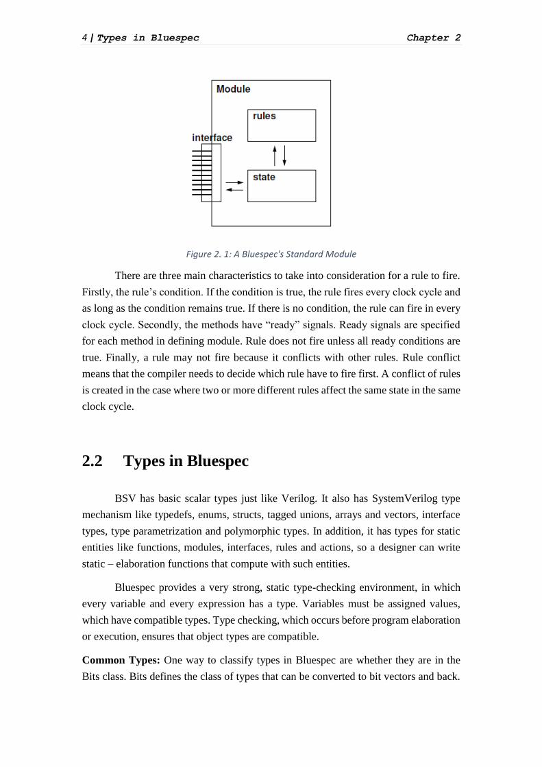
Figure 2. 1: A Bluespec's Standard Module
There are three main characteristics to take into consideration for a rule to fire.
Firstly, the rule’s condition. If the condition is true, the rule fires every clock cycle and
as long as the condition remains true. If there is no condition, the rule can fire in every
clock cycle. Secondly, the methods have “ready” signals. Ready signals are specified
for each method in defining module. Rule does not fire unless all ready conditions are
true. Finally, a rule may not fire because it conflicts with other rules. Rule conflict
means that the compiler needs to decide which rule have to fire first. A conflict of rules
is created in the case where two or more different rules affect the same state in the same
clock cycle.
2.2 Types in Bluespec
BSV has basic scalar types just like Verilog. It also has SystemVerilog type
mechanism like typedefs, enums, structs, tagged unions, arrays and vectors, interface
types, type parametrization and polymorphic types. In addition, it has types for static
entities like functions, modules, interfaces, rules and actions, so a designer can write
static – elaboration functions that compute with such entities.
Bluespec provides a very strong, static type-checking environment, in which
every variable and every expression has a type. Variables must be assigned values,
which have compatible types. Type checking, which occurs before program elaboration
or execution, ensures that object types are compatible.
Common Types: One way to classify types in Bluespec are whether they are in the
Bits class. Bits defines the class of types that can be converted to bit vectors and back.

5 | Types in Bluespec Chapter 2
Only types in the Bits class are synthesizable and can be stored in a state element, such
as a Register or a FIFO.
Bit Types
Bit#(n): n bits.
Int#(n): Signed fixed width (n) representation of an integer value.
UInt#(n): Unsigned fixed width (n) representation of an integer value.
Bool: True or False value.
Non Bit Types
Integer: Integers are unbounded in size and are commonly used as loop
indices for compile-time evaluation.
String: Strings are mostly used in system functions (such as $display).
They can be tested for equality and inequality.
Interface: Since interfaces are considered a type, they can be passed to
and returned from functions
More types: Action, ActionValue, Rules, Modules, Functions.
User Defined Types
Enum: Similar to most languages, a user can define names to be used in
his code. Enum labels must all start with an uppercase letter.
Tagged Union: Tagged unions contain members. A member name must
start with lowercase letter.
Struct: Structures are just like Tagged Unions.
The Bluespec environment strictly checks both bit – width compatibility and
type. Below we present Bluespec’s data type functions that help the designer to convert
across types

6 | The Bluespec Compiler Chapter 2
Figure 2. 2: Bluespec's Data Type conversion functions
Pack: converts (packs) from various types, including Bool, Int, and UInt to Bit.
unpack: converts from Bit to various types, including Bool, Int and UInt.
fromInteger: converts from an Integer to any type where this functions is provided in
the Literal type-class. Integers are most often used during static elaboration since they
cannot be turned into bit; hence, there is no corresponding toInteger function
valueOf: converts from a numeric type to an Integer. Numeric types are the n’s as used
in Bit#(n).
2.3 The Bluespec Compiler
The Bluespec compiler can translate Bluespec descriptions into either Verilog
RTL or a cycle-accurate SystemC simulation (Figure 2.3). It does this by initially eval-
uating the high – level description of the design into a TRS description of rules and
state. From this TRS description, the compiler schedules the actions and transforms the
design into a timing – aware hardware description. This task involves determining when
rules can fire safely and concurrently, adding muxing logic to handle the sharing of
state elements by rules, and finally applying boolean optimizations to simplify the de-
sign. From this timing – aware model, the compiler can then produce a synthesizable
Verilog RTL or SystemC executable output.

7 | The Bluespec Compiler Chapter 2
2.3.1 Scheduling Scheduling is called the task of determining what subset of rules should fire on
a cycle given its state and in what order should rules be fired in a single cycle. Under-
standing how the Bluespec compiler schedules multiple rules for cycle-by-cycle exe-
cution is important for using Bluespec proficiently. Optimal selection of which subset
of firable rules to fire in a single cycle is an NP-hard task, so the Bluespec compiler
resorts to a quadratic time approximation.
Figure 2. 3: Bluespec's Compiler Design Flow
Determining Rule Contents
Due to the complexity of determining when a rule will use an interface of a
module, the Bluespec compiler assumes conservatively that an action will use any
method that it could ever use. That is to say, if an action uses a method only when some
condition is met, the scheduler will treat it as if were always using it. This leads the
compiler to make to conservative estimations of method usage, which in turn causes
conservative firing conditions to be scheduled.

8 | The Bluespec Compiler Chapter 2
Determining Pair-wise Scheduling Conflicts
Once the components (methods and other actions) of all the actions have been
determined, we find all possible conflicts between each atomic action pair. In the case
that two rule predicates are provably disjoint, we can say that there are no conflicts as
they can never happen in the same clock cycle. Otherwise, the scheduling conflicts
between them is exactly the set of scheduling conflicts between any pair of action com-
ponents of each atomic action.
For example, consider rules “rule1” and “rule2” where rule1 reads some register
r1 and rule2 writes it. Registers have the scheduling constraint “_read < _write”, which
means that calls to the _read method calls must happen before the _write method call
in a single cycle. Thus this constraint is reflected in the constraints between rule1 and
rule2 (“rule1 < rule2”). If rule1 were to also write some register r2 and rule2 where to
read it we would have the additional constraint (“rule2 < rule1”). In this there is no
consistent way of ordering the two rules, so we consider the rules conflicting with se-
quential ordering restrictions (as they will never happen together, it doesn’t matter how
they are ordered to happen concurrently).
Generating a Final Global Schedule
Once all the pair-wise conflicts between actions have been determined, a tem-
poral ordering of the actions takes place. For this to happen, the compiler orders the
atomic transactions by some metric of importance, which is called urgency. Scheduler
sorts each action in descending urgency order. The goal is to place the action in a posi-
tion that prevents the most conflicts with already ordered rules in this process. Only
when its ordering has been determined, the rule is allowed to be fired in a cycle, when
respectively its predicate is met and there are no more urgent rules which conflict with
it in that total ordering. Once the compiler has considered all atomic transactions in
sequence, we have a complete schedule.
2.3.2 The Bluesim Simulator Bluesim delivers high-speed simulation of BSV designs at a source – level or
with SystemC executables. Bluesim can be at least 10x faster than the standard Verilog
Simulator. The main features of the simulator is that it has high-speed and the output
of a BSV high-level-design is a source-level or SystemC executable simulation. In ad-
dition, Bluesim is 100% cycle accurate with Verilog RTL and it generates standard
VCD files. Therefore, the benefits of these are that the simulation can be accelerated as
well as the verification of the design.

9 | ARM Scalar Unit Chapter 3
Chapter 3
ARM Scalar Unit
A Reduced Instruction Set Computer (RISC) is a microprocessor that has been
designed to perform a small set of instructions, with the aim of reducing the overall
speed of the processor. The RISC concept first originated in the early 1970’s when an
IBM research team provided that 20% of instruction did 80% of the work. The RISC
architecture follows the philosophy that one instruction should be performed every
clock cycle.
ARM, previously Advanced RISC Machine, originally Acorn RISC Machine,
is a family of reduced instruction set computing (RISC) architectures for computer pro-
cessors, configured for various environments. British company ARM Holdings devel-
ops the architecture and licenses it to other companies, who design their own products
that implement one of those architectures—including systems-on-chips (SoC) and sys-
tems-on-modules(SoM) that incorporate memory, interfaces, radios, etc. It also de-
signs cores that implement this instruction set and licenses these designs to a number
of companies that incorporate those core designs into their own products.
Processors that have a RISC architecture typically require fewer transistors than
those with a complex instruction set computing (CISC) architecture (such as
the x86 processors found in most personal computers), which improves cost, power
consumption, and heat dissipation. These characteristics are desirable for light, porta-
ble, battery-powered devices—including smartphones, laptops and tablet computers,
and other embedded systems. For supercomputers, which consume large amounts of
electricity, ARM could also be a power-efficient solution.
The ARM architecture has been designed to allow very small, yet high-perfor-
mance implementations. The architectural simplicity of ARM processors leads to very
small implementations, and small implementations allow devices with very low power
consumption.
Our implementation of ARM is based on the ARM7 family of processors. Our
processor supports 32-bit architecture, 3-stage pipeline and is based on ARMv4 instruc-
tion set. In the sections below the ARMv4 instructions that were implemented in our
design will be analyzed.

10 | ARM Architecture Chapter 3
3.1 ARM Architecture
As we introduced before, ARM is a Reduced Instruction Set Computer (RISC),
as it incorporates these typical RISC architecture features:
A large uniform register file.
A load/store architecture, where data-processing operations only operate on reg-
ister contents, not directly on memory contents.
Simple addressing modes, with all load/store addresses being determined from
register contents and instruction fields only.
Uniform and fixed-length instruction fields, to simplify instruction decode.
In addition, the ARM architecture provides:
Control over both the Arithmetic Logic Unit (ALU) and shifter in most data-
processing instructions to maximize the use of an ALU and a shifter.
Load and Store multiple instructions to maximize data throughput.
Auto-increment and auto-decrement addressing modes to optimize program
loops.
Conditional execution of almost all instructions to maximize execution through-
put.
These enhancements to a basic RISC architecture allow ARM processors to achieve a
good balance of high performance, low code size and low power consumption.
3.1.1 ARM Processor Modes ARM supports seven operating modes:
User mode (unprivileged mode under which most tasks run).
FIQ mode (entered when a high priority (fast) interrupt is raised).
IRQ mode (entered when a low priority (normal) interrupt is raised).
Supervisor mode (entered on reset and when a Software Interrupt instruction is
executed).
Abort mode (used to handle memory access violations).
Undef mode (used to handle undefined instructions).
System mode (privileged mode using the same registers as user mode).
Most application programs execute in User mode. When the processor is in User
mode, the program being executed is unable to access some protected system resources
or to change mode.
Our design supports only the User mode of ARM processor modes.

11 | ARM Architecture Chapter 3
3.1.2 ARM Registers Arm has 37 registers in total, all of which are 32-bits long.
1 dedicated Program Counter (PC).
1 dedicated Current Program Status Register (CPSR).
5 dedicated Saved Program Status Registers (SPSR).
30 general purpose registers.
Given the fact that our processor only supports user mode, 16 + 1 of these reg-
isters are implemented by the designer. The roles of these 16 registers are specified
below:
R0 – R12 are general purpose registers. Their uses are purely defined by the
software.
R13 is the Stack Pointer (SP) that software normally uses.
R14 is the Link Register (LR). This register holds the address of the next in-
struction after a Branch & Link (BL) instruction, which is the instruction used
to make a subroutine call. In every other case, R14 can be considered a general-
purpose register.
R15 is the Program Counter (PC). In the most instructions, it is used as a pointer
to the instruction that is two steps ahead of the one being executed. In ARM
state, all ARM instructions are four bytes long (32-bit word) and are always
aligned on a word boundary. This means that the two least significant bits of
this register are always zero; therefore, the PC contains 30 non-constant bits
and 2 constant bits.
Figure 3. 1: Arm Register Set

12 | ARM Architecture Chapter 3
The Current Program Status Register (CPSR)
CPSR is accessible in all processor modes. It contains condition code flags, in-
terrupt disable bits, the current processor mode, and other status and control infor-
mation. The format of this register is shown below:
Figure 3. 2: Current Program Status Register Format
The N (Negative), Z (Zero), C (Carry), V (oVerflow) bits are collectively known
as the condition code flags. These flags can be tested by most instructions in order to
determine whether the instruction is to be executed. The condition code flags are usu-
ally modified by:
Execution of comparison instructions (CMN, CMP, TEQ, TST).
Execution of some other data processing instructions, where the desti-
nation register is not R15. Most of these instructions have both a flag-
preserving and a flag-setting variant, with the latter being selected by
adding an S qualifier to the instruction mnemonic. Some of these in-
structions only have a flag-preserving version. This is noted in the indi-
vidual instruction descriptions.
In either case, the new condition code flags (after the instruction has been exe-
cuted) usually mean:
N is set to 1:
When the result of the instruction is regarded as a two’s complement signed
integer and the least significant bit of this result is ‘1’ then it means that the
result is a negative value and the N bit is set. Otherwise, N is set to 0.
Z is set to 1:
When the result of the instruction being executed is zero. This often indicates
an equal result from a comparison. In any other case, Z is set to 0.
C is set to 1:
When an addition instruction (including the comparison instruction CMN) pro-
duces a carry.
When a subtraction instruction (including the comparison instruction CMP)
produces a borrow.
When a non-addition/subtraction instruction (e.g. MOV), that incorporates a
shift operation, makes the last bit of the result shifted out of the value.
In any other case C is set to 0.

13 | ARM v4 Instruction Set Architecture Chapter 3
V is set to 1:
When an addition or subtraction instruction occurs a signed overflow, regard-
ing the operands and result as two’s complement signed integers. Otherwise,
V is set to 0.
The bottom eight bits that we can observe in the CPSR format represent the following:
Interrupt Disable bits:
I = 1 Disables the IRQ interrupts.
F = 1 Disables the FIQ interrupts.
T – Bit (Architecture v4T only):
T = 0 Processor is executing in ARM state.
T = 1 Processor is executing in Thumb state.
Mode Bits:
Mode Defines the processor mode. Not all combinations of the mode
bits define a valid processor mode so take care to use the right combi-
nations.
Since our design does not support other processor modes or interrupts, we only care
about the N, Z, C, V flags of the CPSR.
3.2 ARM v4 Instruction Set Architecture
Figure below shows the ARM Instruction Set Format. In the next sections of
this thesis, we will only describe the instructions that our processor supports.
Figure 3. 3: ARM Instruction Set Format

14 | ARM v4 Instruction Set Architecture Chapter 3
3.2.1 Conditional Execution In ARM state, all instructions are conditionally executed according to the state
of the CPSR condition code and the instruction’s condition field. This field (bits 31:28)
determines the circumstances under which an instruction is to be executed. If the state
of the C, N, Z and V flags fulfils the conditions encoded by the field, the instruction is
executed, otherwise it is ignored. The conditional execution can be translated as the
figure below shows:
Figure 3. 4: Condition Codes & Conditional Execution
3.2.2 Shifts & Rotates ARM architecture does not support actual shift or rotate instructions. Instead, it
uses a barrel shifter, which provides a mechanism to carry out shifts as a part of other
instructions. Barrel shifter is responsible for the following operations:
LSL: Logical Shift Left.
LSR: Logical Shift Right.
ASR: Arithmetic Shift Right Shifts right and preserves the sign bit for 2’s
complement operations.
ROR: Rotate Right.

15 | ARM v4 Instruction Set Architecture Chapter 3
3.2.3 Branch and Branch with Link (B, BL) The encoding of such instructions is shown in the figure below:
Figure 3. 5: ARM Branch Instructions Encoding
Branch instructions contain a signed 2’s complement 24 bit offset. This is
shifted left two bits, sign extended to 32 bits, and added to the Program Counter (PC).
The instruction can therefore specify a branch of +/- 32Mbytes. The branch offset must
take account of the prefetch operation, which causes the PC to be 2 words (8 bytes)
ahead of the current instruction.
Branches beyond +/- 32Mbytes must use an offset or absolute destination,
which has been previously loaded into a register. In this case, the PC should be manu-
ally saved in Link Register (LR) if a Branch with Link type operation is required.
The Link Bit
Branch with Link (BL) writes the old PC into the Link Register (LR) of the
current register bank. The PC value written into LR is adjusted to allow for the prefetch,
and contains the address of the instruction following the branch and link instruction. To
return from a routine called by BL, use MOV PC, LR if the link register is still valid.
3.2.4 Data Processing ARM supports 16 data-processing instructions shown in figure below:
Figure 3. 6: ARM Data Processing Instructions

16 | ARM v4 Instruction Set Architecture Chapter 3
The encoding of these instructions is shown in figure below:
Figure 3. 7: ARM Data Processing Instructions Encoding
A data processing instruction produces a result by performing a specified arith-
metic or logical operation on one or two operands. The first operand is always a register
(Rn). The second operand may be a shifted register (Rm) or a rotated 8-bit immediate
value (Imm) according to the value of the I bit in the instruction encoding. The condi-
tion codes in the CPSR may be preserved or updated as a result of this instruction,
according to the value of the S bit in the instruction encoding.
Certain operations (TST, TEQ, CMP, CMN) do not write the result to the des-
tination register (Rd). They are used only to perform tests and to set the condition codes
on the result and always have the S bit set.
The data processing operations may be classified as logical or arithmetic. The
logical operations (AND, EOR, TST, TEQ, ORR, MOV, BIC, MVN) perform the log-
ical action on all corresponding bits of the operand or operands to produce the result. If
the S bit is set, the V-flag in the CPSR will be unaffected, the C-flag will be set to the
carry out from the barrel shifter, the Z-flag will be set if and only if the result is all
zeros, and the N-flag will be set to the logical value of bit 31 of the result.
The arithmetic operations (SUB, RSB, ADD, ADC, SBS, RSC, CMP, CMN)
treat each operand as a 32 bit integer. If the S bit is set the V-flag in the CPSR will be
17 | ARM v4 Instruction Set Architecture Chapter 3
set if an overflow occurs into bit 31 of the result, the C-flag will be set to the carry out
of bit 31 of the ALU, the Z-flag will be set if and only if the result was zero, and the N-
flag will be set to the value of bit 31 of the result.
Shifts
When the second operand is specified to be a shifted register, the operation of
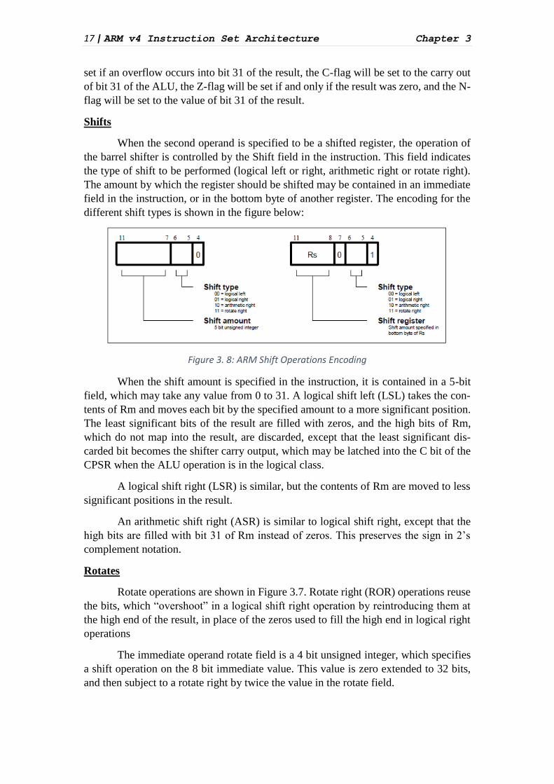
the barrel shifter is controlled by the Shift field in the instruction. This field indicates
the type of shift to be performed (logical left or right, arithmetic right or rotate right).
The amount by which the register should be shifted may be contained in an immediate
field in the instruction, or in the bottom byte of another register. The encoding for the
different shift types is shown in the figure below:
Figure 3. 8: ARM Shift Operations Encoding
When the shift amount is specified in the instruction, it is contained in a 5-bit
field, which may take any value from 0 to 31. A logical shift left (LSL) takes the con-
tents of Rm and moves each bit by the specified amount to a more significant position.
The least significant bits of the result are filled with zeros, and the high bits of Rm,
which do not map into the result, are discarded, except that the least significant dis-
carded bit becomes the shifter carry output, which may be latched into the C bit of the
CPSR when the ALU operation is in the logical class.
A logical shift right (LSR) is similar, but the contents of Rm are moved to less
significant positions in the result.
An arithmetic shift right (ASR) is similar to logical shift right, except that the
high bits are filled with bit 31 of Rm instead of zeros. This preserves the sign in 2’s
complement notation.
Rotates
Rotate operations are shown in Figure 3.7. Rotate right (ROR) operations reuse
the bits, which “overshoot” in a logical shift right operation by reintroducing them at
the high end of the result, in place of the zeros used to fill the high end in logical right
operations
The immediate operand rotate field is a 4 bit unsigned integer, which specifies
a shift operation on the 8 bit immediate value. This value is zero extended to 32 bits,
and then subject to a rotate right by twice the value in the rotate field.

18 | ARM v4 Instruction Set Architecture Chapter 3
3.2.5 Multiply and Multiply-Accumulate (MUL, MLA) The encoding of such instructions is shown in the figure below:
Figure 3. 9: ARM Multiply Instructions Encoding
The multiply form of the instruction gives Rd:=Rm*Rs. Rn is ignored and
should be set to zero for compatibility.
The multiply-accumulate form of the instruction gives Rd:=Rm*Rs + Rn, which
can save an explicit ADD instruction in some circumstances.
Both forms of the instruction work on operands which may be considered as
signed (2’s complement) or unsigned integers.
The results of a signed multiply and of an unsigned multiply of 32 bit operands
differ only in the upper 32 bits – the low 32 bits of the signed and unsigned results are
identical. As these instructions only produce the low 32 bits of a multiply, they can be
used for both signed and unsigned multiplies.
The destination register Rd must not be the same as the operand register Rm.
All other register combinations will give correct results, and Rd, Rn, and Rs may use
the same register when required.
Setting the CPSR flags is optional, and is controlled by the S bit in the instruc-
tion. The N (Negative) and Z (Zero) flags are set correctly on the result (N is made
equal to bit 31 of the result, and Z is set if and only if the result is zero). The C (Carry)
flag is set to a meaningless value and the V (oVerflow) flag is unaffected.
3.2.6 Multiply Long and Multiply-Accumulate Long (MULL,
MLAL) The encoding of such instructions is shown in the figure below:
Figure 3. 10: ARM Multiply Long Instructions Encoding

19 | ARM v4 Instruction Set Architecture Chapter 3
The multiply long instructions perform integer multiplication on two 32 bit op-
erands and produce 64 bit results. Signed and unsigned multiplication each with op-
tional accumulate give rise to four variations.
The multiply forms (UMULL and SMULL) take two 32 bit numbers and mul-
tiply them to produce a 64 bit result of the form RdHi,RdLo := Rm*Rs. The lower 32
bits of the 64-bit result are written to RdLo, the upper 32 bits of the result are written
to RdHi.
The multiply-accumulate forms (UMLAL and SMLAL) take two 32 bit num-
bers, multiply them and add a 64 bit number to produce a 64 bit result of the form
RdHi,RdLo := Rm*Rs + RdHi,RdLo. The lower 32 bits of the 64 bit number to add is
read from RdLo. The upper 32 bits of the 64 bit number to add is read from RdHi. The
lower 32 bits of the 64 bit result are written to RdLo. The upper 32 bits of the 64 bit
result are written to RdHi.
The UMULL and UMLAL instructions treat all of their operands as unsigned
binary numbers and write an unsigned 64 bit result. The SMULL and SMLAL instruc-
tions treat all of their operands as two’s-complement signed numbers and write a two’s-
complement signed 64 bit result.
Setting the CPSR flags is optional, and is controlled by the S bit in the instruc-
tion. The N and Z flags are set correctly on the result (N is equal to bit 63 of the result,
Z is set if and only if all 64 bits of the result are zero). Both the C and V flags are set to
meaningless values.
3.2.7 Single Data Transfer (LDR, STR) The encoding of such instructions is shown in figure below:
Figure 3. 11: ARM Single Data Transfer Instructions Encoding

20 | ARM v4 Instruction Set Architecture Chapter 3
The single data transfer instructions are used to load or store single bytes or
words of data. The memory address used in the transfer is calculated by adding an offset
to or subtracting an offset from a base register. The result of this calculation may be
written back into the base register if auto-indexing is required.
Offsets and auto-indexing
Either the offset from the base may be a 12 bit unsigned binary immediate value
in the instruction, or a second register (possibly shifted in some way). The offset may
be added to (U = 1) or subtracted from (U = 0) the base register Rn. The offset modifi-
cation may be performed either before (pre-indexed, P = 1) or after (post-indexed, P =
0) the base is used as the transfer address.
The W bit gives optional auto increment and decrement addressing modes. The
modified base value may be written back into the base (W=1), or the old base value
may be kept (W=0). In the case of post-indexed addressing, the write back bit is redun-
dant and is always set to zero, since the old base value can be retained by setting the
offset to zero. Therefore, post-indexed data transfers always write back the modified
base. The only use of the W bit in a post-indexed data transfer is in privileged mode
code, where setting the W bit forces non-privileged mode for the transfer, allowing the
operating system to generate a user address in a system where the memory management
hardware makes suitable use of this hardware.
The 8 shift control bits are described in the data processing instructions section.
However, the register specified shift amounts are not available in this instruction class.
Addressing Modes
In these instructions, the addressing mode is formed from two parts, the base register
and the offset. The base register can be any of the general-purpose registers. The offset
can take one out of three formats:
1. Immediate: The offset is an unsigned number that can be added to or subtracted
from the base register. Immediate offset addressing is useful for accessing data
elements that are a fixed distance from the start of the data object, such as struc-
ture fields, stack offsets and input/output register. For the word and unsigned
byte instructions, the immediate offset is a 12 bit number. For the halfword and
signed byte instructions, it is a 8 bit number.
2. Register: The offset is a general-purpose register that can be added to or sub-
tracted from the base register. Register offset are useful for accessing arrays or
blocks of data.
3. Scaled Register: The offset is a general purpose register, shifted by an imme-
diate value, then added to or subtracted from the base register. The same shift
operations used for data processing instructions can be used. Therefore, Logical
Shift Left (LSL) is the most useful as it allows an array indexed to be scaled by
the size of each array element. Scaled register offsets are only available for the
word and unsigned byte instructions.

21 | ARM v4 Instruction Set Architecture Chapter 3
As well as the three types of offset, the offset and the base register are used in three
different ways to form the memory address:
1. Offset: The base register and offset are added or subtracted to form the memory
address.
2. Pre-Indexed: The base register and offset are added or subtracted to form the
memory address. The base register is then updated with this new address to al-
low automatic indexing through an array or memory block.
3. Post-Indexed: The value of the base register alone is used as the memory ad-
dress. The base register and offset are then added or subtracted, and this value
is stored back in the base register, to allow automatic indexing through an array
or memory block.
Figure below shows a theoretical datapath of an ARMv4 processor
Figure 3. 12: ARM Theoretical Datapath

22 | ARM Vector Unit Chapter 4
Chapter 4
ARM Vector Unit
In computing, a vector processor or array processor is a central processing unit
(CPU) that implements an instruction set containing instructions that operate on one-
dimensional arrays of data called vectors, compared to scalar processors, whose instruc-
tions operate on single data items. Vector processors can greatly improve performance
on certain workloads, notably numerical simulation and similar tasks.
As of 2015, most commodity CPUs implement architectures that feature in-
structions for a form of vector processing on multiple (vectorized) data sets, typically
known as SIMD (Single Instruction, Multiple Data). Common examples include Intel
x86’s MMX, SSE, AVX instructions and ARM NEON.
Vector processing techniques have since been added to almost all modern CPU
designs, although they are typically referred to as SIMD (differing in that a single in-
struction always drives a single operation across a vector register, as opposed to the
more flexible latency hiding approach in true vector processors). In these implementa-
tions, the vector unit runs beside the main scalar CPU, providing a separate set of vector
registers, and is fed data from vector instruction aware programs.
Single Instruction, Multiple Data (SIMD), is a class of parallel computers in
Flynn’s taxonomy. It describes computers with multiple processing elements that per-
form the same operation on multiple data points simultaneously. Thus, such machines
exploit data level parallelism, but not concurrency: these are simultaneous (parallel)
computations, but only a single process (instruction) at a given moment. SIMD is par-
ticularly applicable to common tasks such as adjusting the contrast in a digital image
or adjusting the volume of digital audio.
Figure 4. 1: A typical Vector Processing Unit

23 | Comparing Scalar to Vector Chapter 4
4.1 Comparing Scalar to Vector
In a traditional scalar processor, the basic data type is an n-bit word. The archi-
tecture often exposes a register file of words, and the instruction set is composed of
instructions that operate on individual words.
In a vector architecture, there is support of a vector datatype, where a vector is
a collection of VL n-bit words (VL is the vector length). They may also be a vector
register file, which was a key innovation of the Cray architecture.
Figures below illustrate the difference between vector and scalar data types, and
the operations that can be performed on them.
Figure 4. 2: (A): A 64-bit scalar register, and (B): A vector register of 8 64-bit elements
We can say that a vector register “holds the values of n scalar registers”. As we
can see in the figure above a vector register can hold eight discrete and different values
as long as a scalar register can hold one. The concept is that with a single instruction a
designer can perform the same operation on multiple data elements as it is shown in
figure below.
Figure 4. 3: Difference between scalar and vector add instructions

24 | Vector Architecture Chapter 4
4.2 Vector Architecture
The main characteristic of a vector architecture is that they provide high-level
operations that work on vectors. Vector is a linear array of elements. The length of the
array varies, depending on hardware. A vector processor means that an instruction op-
erates on multiple data elements in consecutive time steps.
In order to exploit the extra features of the vector processors, the calculations
made should not depend on previous results in each clock cycle. The great power of
vector processors is that they can replace simple loops with commands. This in itself
helps to avoid control hazards, ensuring the conditions for developing a compact code
with less chance of errors. To do this, the data in the main memory must be in a speci-
fied pattern. The ideal would be to be located in neighboring memory locations.
4.2.1 Components of a Vector Processor
Vector Registers: Each register is an array of elements. They actually com-
pose a fixed length bank holding a single vector. They need at least two read
and one write port. Typically, they are 8-32 vector registers, each holding 64-
128 64-bit elements.
Vector Functional Units (Vector ALUs): These modules are fully pipelined
and start a new operation every clock.
Scalar Design: The SIMD unit operates among with the Scalar unit.
4.2.2 Advantages of Vector Instruction Set Architecture No dependencies within a vector
o Pipelining, parallelization works well.
o Can have very deep pipelines, no dependencies.
Each instruction generates a lot of work.
o Strengthens instruction level parallelism.
o Reduces instruction fetch bandwidth.
Highly regular memory access pattern.
o Interleaving multiple banks for higher memory band-
width.
No need to explicitly code loops.
o Fewer branches in the instruction sequence.

25 | Our Vector Instruction Set Architecture Chapter 4
4.3 Our Vector Instruction Set Architecture
Figure below illustrates our vector processor’s Instruction Set Format. In the
sections below, we will describe every vector instruction that our processor supports.
Figure 4. 4: Our Vector Instruction Set Format
With regard to our own design and the figure above, we have implemented a
vector processing unit that executes the basic SIMD instructions (Vector Data Pro-
cessing, Vector Multiply/Vector Multiply-Accumulate and Vector Load/Store). Our
vector processing unit can perform two vector instructions in parallel. The main com-
ponents of our vector processing unit are listed below:
A Vector Register File, which is composed by 15 vector registers each of them
holds 8 128-bit elements.
Two Vector Barrel Shifters, which are responsible for shift operations that an
instruction may demand.
Two Vector Functional Units (ALUs), which are responsible for executing the
operation on two elements of two vector registers.
** We created two ALU’s (and so two barrel shifters) in order to be able to execute two
vector processing instructions in parallel. **
A vector instruction takes eight clock cycles in order to be fully executed. Every
cycle we perform this instruction on each element of our vector registers. We introduce
an example for a vector add (VADD) instruction. In a VADD instruction we need to
read the two operands (vector registers), perform the operation and write the result to
the destination register. Therefore, in the first cycle we read the first element of the
vector_register_operand_1, the first element of the vector_register_operand_2, we add

26 | Our Vector Instruction Set Architecture Chapter 4
them and finally we write the result to the first element of the destination_vector_reg-
ister. In the second and in the other six cycles we do the same thing by chancing the
elements that we operate on (2nd cycle 2nd elements of the vector registers and so
on).
In the figure below, we can see the example of a vector add (VADD) instruction
in our vector processor:
Figure 4. 5: Vector Add (VADD) Instruction Example
4.3.1 Vector Data Processing Our vector processing unit supports 9 general data processing instructions that
are shown in the figure below:
Figure 4. 6: Our Vector General Data Processing Instructions

27 | Our Vector Instruction Set Architecture Chapter 4
The encoding of these instructions is shown in the figure below:
Figure 4. 7: Our Vector General Data Processing Instructions Encoding
A vector data processing instruction produces eight discrete results by perform-
ing a specified arithmetic or logical operation on one or two elements of one or two
operands. The first operand is always a vector register (Vn). The second operand may
be a shifted vector register (Vm) or a rotated 8-bit immediate value (Imm) according to
the value of the I bit in the instruction encoding.
The vector data processing operations may be classified as vector logical or
vector arithmetic. The vector logical operations (VAND, VEOR, VORR, VMOV,
VBIC, and VMVN) perform the logical action on all corresponding bits of the operand
or operands to produce the result.
The vector arithmetic operations (VSUB, VRSB, and VADD) treat each oper-
and as a 128 bit integer.

28 | Our Vector Instruction Set Architecture Chapter 4
Shifts
When the second operand is specified to be a shifted vector register, the opera-
tion of the vector barrel shifter is controlled by the Shift field in the instruction. This
field indicates the type of shift to be performed (logical left or right, arithmetic right or
rotate right). The amount by which the vector register should be shifted may be con-
tained in an immediate field in the instruction, or in the bottom bits of another register.
The encoding for the different shift types is shown in the figure below:
Figure 4. 8: Our Vector Shift Operations Encoding
When the shift amount is specified in the instruction, it is contained in a 6-bit field,
which may take any value from 0 to 63. A logical shift left (LSL) takes the contents of
every Vm element and moves each bit by the specified amount to a more significant
position. The least significant bits of the result are filled with zeros, and the high bits
of every element of Vm, which do not map into the result, are discarded.
A logical shift right (LSR) is similar, but the contents of every element of Vm
are moved to less significant positions in the result.
An arithmetic shift right (ASR) is similar to logical shift right, except that the
high bits are filled with bit 127 of every element of Vm instead of zeros. This preserves
the sign in 2’s complement notation.
Rotates
Rotate operations are shown in Figure 4.7. Rotate right (ROR) operations reuse
the bits that “overshoot” in a logical shift right operation by reintroducing them at the
high end of the result, in place of the zeros used to fill the high end in logical right
operations
The immediate operand rotate field is a 4 bit unsigned integer that specifies a
shift operation on the 8 bit immediate value. This value is sign extended to 128 bits,
and then subject to a rotate right by twice the value in the rotate field.

29 | Our Vector Instruction Set Architecture Chapter 4
4.3.2 Vector Multiply and Vector Multiply-Accumulate
(VMUL, VMLA) The encoding of such instructions is shown in the figure below:
Figure 4. 9: Our Vector Multiply Instructions Encoding
The multiply form of the instruction gives Vd:=Vm*Vs. Vn is ignored and
should be set to zero for compatibility.
The multiply-accumulate form of the instruction gives Vd:=Vm*Vs + Vn,
which can save an explicit VADD instruction in some circumstances.
Both instructions operate on the same element of the operand vector register.
For example the multiply instruction will multiply the first element of Vm vector reg-
ister with the first element of the Vs vector register and store the result on the first
element of Vd vector register and so on.
Both forms of the instruction work on operands which may be considered as
signed (2’s complement) or unsigned integers.
The results of a signed multiply and of an unsigned multiply of 128 bit operands
differ only in the upper 128 bits – the low 128 bits of the signed and unsigned results
are identical. As these instructions only produce the low 128 bits of a multiply, they
can be used for both signed and unsigned multiplies.
The destination vector register Vd must not be the same as the operand vector
register Vm. All other vector register combinations will give correct results, and Vd,
Vn, and Vs may use the same vector register when required.

30 | Our Vector Instruction Set Architecture Chapter 4
4.3.3 Vector Load and Vector Store (VLD, VST) Our vector processing unit also supports Vector Load (VLD) and Vector Store
(VST) instructions. The encoding of such instructions is shown in the figure below:
Figure 4. 10: Our Vector Load/Store Instructions Encoding
Our vector load and store instructions are implemented according to ARM
NEON architecture and are modified to work to our own design.
NEON structure loads read data from memory into registers, with optional de-
interleaving. Stores work similarly, reinterleaving data from registers before writing it
to memory.
The structure load and store instructions have a syntax consisting of five parts:
The instruction mnemonic, which is either VLD for loads or VST for
stores.
A numeric interleave pattern, the gap between corresponding elements
in each structure.
An element type, specifying the number of bits in the accessed elements.
A set of vector registers to be read or written. Up to four registers can
be listed, depending on the interleave pattern.
An ARM address register, containing the location to be accessed in
memory.

31 | Our Vector Instruction Set Architecture Chapter 4
Instructions are available to load, store and deinterleave structures containing
from one to four equally sized elements, where the elements are the supported widths
of 8, 16 or 32 bits.
Interleave = 1: It loads one to four registers of data from memory, with
no deinterleaving.
Interleave = 2: It loads two or four registers of data, deinterleaving even
and odd elements into those registers.
Interleave = 3: It loads three registers and deinterleaves.
Interleave = 4: It loads four registers and deinterleaves.
Stores support the same options, but interleave the data from registers before
writing them to memory.
Loads and stores interleave elements based on the size specified to the instruc-
tion.
Element type = 1: We load the 8 bottom bits of the address specified in
the ARM register and sign extend it to 128 bits.
Element type = 2: We load the 16 bottom bits of the address specified
in the ARM register and sign extend it to 128 bits.
Element type = 3: We load the entire 32 bits of the address specified in
the ARM register and sign extend it to 128 bits.
Element type = 4: We load the entire 32 bits of the address specified in
the ARM register and sign extend it to 128 bits.
Our design supports vector load and store instructions but not of all kinds. It
supports Load/Store in only one vector register with interleaving = 1 and every element
type.
Below we will explain with examples how our design work on Vector Load and
Vector Store instructions:
Example of a load:
We read the contents of the Rm register in order to obtain the address we need to load
on our Vd1 vector register. With interleaving = 1 (i.e. serial reads in memory) we load
the contents that we read from memory into every element of our vector register. So if
the value of Rm = 0 then we load into Vd1 [0] the contents of MEM [0], into Vd1 [1]
the contents of MEM [1], into Vd1 [2] the contents of MEM [2] and so on.

32 | Our Vector Instruction Set Architecture Chapter 4
Example of a store:
We read the contents of the Rm register in order to obtain the address we need to store
on our Vd1 vector register. With interleaving = 1 (i.e. serial writes in memory) we store
the contents that we read from every element of our vector register into memory. So if
the value of Rm = 0 then we store into MEM [0] the contents of Vd1 [0], into MEM [1]
the contents of Vd1 [1], into MEM [2] the contents of Vd1 [2] and so on.
Figure below shows a theoretical datapath of a Vector Processor:
Figure 4. 11: Theoretical Datapath of a Vector Processing Unit

33 | Implementation Chapter 5
Chapter 5
Implementation
In this section, we will analyze and explain the structural components of our
processor. Our design supports a 3-stage pipeline (Fetch – Decode – Execute) in order
to increase the speed of the flow of instructions to the processor. This allows several
operations to take place simultaneously, and the processing, and memory systems to
operate continuously. Figure bellow illustrates our processor’s pipeline:
Figure 5. 1: ARM 3-Stage Pipeline
As we described in previous sections, our design supports a scalar and a vector
processing unit. The scalar processing unit supports all Data Processing instructions,
Branch and Branch and Link instructions, Load and Store instructions with offset in-
dexed addressing (post and pre indexed) and six instructions of multiplication (Multi-
ply/Multiply Accumulate, Signed and Unsigned Multiply Long/Multiply Long Accu-
mulate). The vector processing unit supports some of the Vector Data Processing in-
structions (as we are not concerned about conditional execution on a vector processor
we did not implement the instructions that just set the CPSR), Vector Multiply and
Vector Multiply Accumulate instructions and the Vector Load and Store ones.
Since all of these instructions are integer type with single-cycle execution la-
tency, we conclude that there is no need to deal with data forwarding (scalar part) or
chaining (vector part).

34 | Scalar Implementation Chapter 5
Below we present a general block diagram (datapath) of our architecture.
Figure 5. 2: Datapath of the Design
5.1 Scalar Implementation
In this sub-section, we will fully describe the functionality of every module of
the scalar design. The modules that compose this design are Instruction Memory, De-
code, Barrel Shifter, ALU, Multiplier, Register File and the Data Memory module.
5.1.1 Instruction Memory Module Instruction memory is implemented as Bluespec’s internal storage and data
structure library “RegFile”. This package defines one interface that provides two meth-
ods, “upd” and “sub”. The “upd” method is an Action method used to modify (or up-
date) the value of an element in the storage. The “sub” method is a Value method that
reads and returns the value of an element in the storage. From the “RegFile” package
we make use of “mkRegFileFullLoad” module, which creates a memory from min to
max index (0 – 1023 in our case) using a file to provide its initial contents.
In our design, we load in the memory a .bin or a .hex (whatever we prefer) file
of instructions. This file is then read, row by row, with the use of the provided method
“sub” and the execution starts.
35 | Scalar Implementation Chapter 5
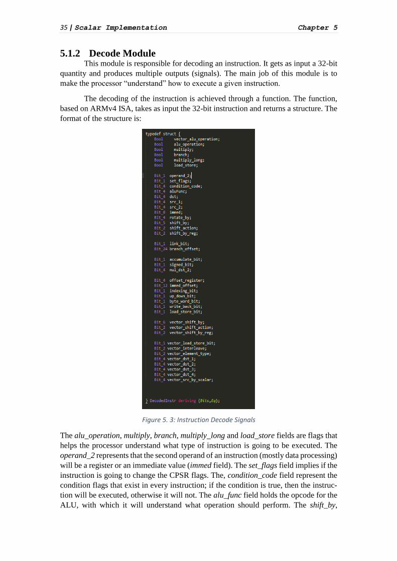
5.1.2 Decode Module This module is responsible for decoding an instruction. It gets as input a 32-bit
quantity and produces multiple outputs (signals). The main job of this module is to
make the processor “understand” how to execute a given instruction.
The decoding of the instruction is achieved through a function. The function,
based on ARMv4 ISA, takes as input the 32-bit instruction and returns a structure. The
format of the structure is:
Figure 5. 3: Instruction Decode Signals
The alu_operation, multiply, branch, multiply_long and load_store fields are flags that
helps the processor understand what type of instruction is going to be executed. The
operand_2 represents that the second operand of an instruction (mostly data processing)
will be a register or an immediate value (immed field). The set_flags field implies if the
instruction is going to change the CPSR flags. The, condition_code field represent the
condition flags that exist in every instruction; if the condition is true, then the instruc-
tion will be executed, otherwise it will not. The alu_func field holds the opcode for the
ALU, with which it will understand what operation should perform. The shift_by,

36 | Scalar Implementation Chapter 5
shift_action, shift_by_reg are flags for understanding if a shift operation must happen
and where it should happen (on immediate or on the value of another register). Link_Bit
and branch_offset fields are used for branch instructions. Accumulate_bit, signed_bit
and mul_dst_2 are extra fields that multiply or multiply long (with or without accumu-
lation) instructions have. Offset_register, immed_offset, indexing_bit, up-down_bit,
byte_word_bit, write_back_bit and load_store_bit are fields that help the processor un-
derstand how to execute correctly a load or a store instruction. The other fields of this
module are used for the execution of a vector processing instruction because vector unit
decodes a vector instruction with the same module and way that scalar unit does.
5.1.3 Barrel Shifter Module This module is responsible for performing a shift or a rotate operation on an
operand. The operation is executed by a function, whose syntax is:
function BrlResult scalar_barrel (Bit_32 data, Bit_2 control, Bit_5 by);
For each value of the control argument, the function performs a different action
on the data argument, given the by argument, as follows:
Control == 2’b00 Logical Shift Left (LSL) The function performs a logi-
cal shift left operation on the data argument by the by argument’s bits.
Control == 2’b01 Logical Shift Right (LSR) The function performs a log-
ical shift right operation on the data argument by the by argument’s bits.
Control == 2’b10 Arithmetic Shift Right (ASR) The function performs an
arithmetic shift right operation on the data argument by the by argument’s bits.
Control == 2’b11 Rotate Bits Right (ROR) The function performs a right
rotation on the data argument by the by argument’s bits
The output of the barrel shifter’s function is a struct of a result and carry bit.
5.1.4 ALU Module This module is responsible for executing all Data Processing instructions on the
scalar unit of the processor and for deciding what the CPSR flags should be. More
specifically, the functions (and their syntax) that constitute this module are the follow-
ing:
function ResultT scalar_operation (Bit_32 input_a, Bit_32 input_b, Bit_1 carry_bit,
Bit_4 opcode);
This function is actually performing the execution of the instruction. It takes as
arguments the two operands (input_a, input_b), which are 32 bit, a carry_bit (for in-
structions that need carry) and the opcode, which is responsible to inform the function

37 | Scalar Implementation Chapter 5
what operation should execute. In the body of this function there are other functions
that are called, and decide the result of the operation and the condition flags that the
instruction produces. Such functions are:
function Bit_33 add_op (Bit_33 a, Bit_33 b);
return (a + b);
endfunction
As we can observe, these functions are the “result calculating” functions that
take as arguments only the two operands (a and b), which are the same with the previous
function’s operands (input_a and input_b). They are 33 bit in order to check for the
carry flag. Other functions like this are sub_op, addc_op, subc_op, and_op, or_op,
xor_op, not_op, bitc_op etc. These functions actually calculate the result of a logical or
an arithmetic operation.
Other functions that are called on the body of the main function (scalar_opera-
tion) are the “flags’ calculating” functions. The job of these is to decide what value the
CPSR flags should have, according to the result produced by the functions above. Such
functions are:
Check_carry As its name betrays, this function checks if the result of an
operation produces a carry.
Check_negative This function checks if the result of an operation is negative.
Check_zero This function checks if the result of an operation is zero.
Check_ovf This function checks if an overflow occurs after the operation is
performed.
To summarize, this module is composed by a main function that calculates the
result of an operation and decides what the CPSR flags should be by calling other sub-
functions. The output of the function, like we present below is a struct, which holds the
value of the result and the Zero, Negative, Overflow and Carry flags.
typedef struct {Bit_32 result;
Bit_1 zero;
Bit_1 negative;
Bit_1 overflow;
Bit_1 carry;
} ResultT deriving (Bits, Eq);

38 | Scalar Implementation Chapter 5
5.1.5 Multiplier Module This module is responsible for the multiplication instructions. Such instructions
are Multiply, Multiply and Accumulate, Signed Multiply Long, Signed Multiply Long
and Accumulate, Unsigned Multiply Long and Unsigned Multiply Long and Accumu-
late. These operations are implemented through two different functions on this module.
These functions are:
function ResultT_mul multiply (Bit_1 control, Bit_32 data_1, Bit_32 data_2, Bit_32
data_accumulate);
The function above performs Multiply and Multiply and Accumulate opera-
tions. It takes as arguments a 1-bit control, with which the function determines what
operation from the previous ones should perform, the two operands (data_1 and data_2)
that the multiplication will be performed and data_accumulate argument, which is the
extra operand that the accumulate instructions need in order to be executed. With regard
to control argument, the operations are executed as follows:
Control == 0 Multiply
Control == 1 Multiply and Accumulate
This function also, optionally, decide what the CPSR flags should be, given the
result that was produced.
The output of the function, as we can observe below, is a struct that provides
the result and the Negative, Zero, Carry and Overflow flags.
typedef struct {Bit_32 result_mul;
Bit_1 zero_mul;
Bit_1 negative_mul;
Bit_1 overflow_mul;
Bit_1 carry_mul;
} ResultT_mul deriving (Bits, Eq);
function ResultT_mul_long multiply_long (Bit_2 control, Bit_32 data_1, Bit_32
data_2, Bit_32 data_1_accumulate, Bit_32 data_2_accumulate);
The function above performs Signed Multiply Long, Signed Multiply Long and
Accumulate, Unsigned Multiply Long and Unsigned Multiply Long and Accumulate.
It takes as arguments a 2-bit control, with which the function determines what operation
from the previous ones should perform, the two operands (data_1 and data_2) that the
multiplication will be performed and data_1_accumulate and data_2_accumulate ar-
guments, which are the extra operands that the accumulate instructions need in order to
be executed. Since the result of a multiply long instruction is 64 bit, we need to concat-
enate the values of these two accumulation arguments.
This function also, optionally, decide what the CPSR flags should be, given the
result that was produced.

39 | Scalar Implementation Chapter 5
The output of the function as we can observe below is a struct that provides the
result and the Negative, Zero, Carry and Overflow flags.
typedef struct {Bit_64 result_mul;
Bit_1 zero_mul;
Bit_1 negative_mul;
Bit_1 overflow_mul;
Bit_1 carry_mul;
} ResultT_mul_long deriving (Bits, Eq);
5.1.6 Register File Module This module forms the main “memory core” of the scalar unit of the processor.
It is the main place (along with data memory) that every result of an executed instruc-
tion is stored and/or reused. It is composed from vector of 15 registers (general-purpose
registers, stack pointer and link register) alongside with two extra registers (program
counter and current program status register). Registers in Bluespec can store any type
of data like integers, bits, strings, even whole structures of data. In our design, each
register of the register file holds a 32-bit quantity. The interface of this module has one
method for writing to register file (in some cases we write to two registers simultane-
ously, e.g. Load instruction that also updates the value of the base register), and six
methods for reading (3 needed for data processing instructions, +1 for multiply long
instructions, +2 for vector load and store instructions that get their address by a register
on the scalar unit). Program Counter and Current Program Status Register have their
own read and write ports. The location of reading or writing the data as long as the data
themselves are given to methods as arguments. Below we present the interface of the
register file.
interface RegFile_IFC;
method Bit_32 read_pc();
method Bit_32 read_reg1(Bit_4 read_addr1);
method Bit_32 read_reg2(Bit_4 read_addr2);
method Bit_32 read_reg_accumulate(Bit_4 read_addr3);
method Bit_32 read_reg_accumulate_2(Bit_4 read_addr4);
method Bit_32 read_reg_for_vector_load_store (Bit_4 addr);
method Bit_32 read_reg_for_vector_load_store_2 (Bit_4 addr);
method Action write_reg(Bit_4 write_addr, Bit_32 data, Bool
write_enable, Bit_3 control, Bit_4 write_addr_2, Bit_32 data_2,
Bit_32 new_pc_addr);

40 | Vector Implementation Chapter 5
method Action update_cpsr (Bit_1 negative, Bit_1 zero, Bit_1 carry,
Bit_1 overflow);
method Bit_32 read_cpsr();
endinterface
Read_pc method returns the value of the Program Counter. The other read meth-
ods actually do the same thing, which is to read the value of a specific register on the
register bank, given its address (read_addr). Write_reg method actually writes the data,
which are provided as arguments (data, data_2), to specific registers, whose addresses
are also provided as arguments (write_addr, write_addr_2). Control argument helps to
write the data to the right registers because sometimes there is a need to write to the
program counter (e.g. branches).
Below we present the vectors and the registers of the register file.
Vector#(15, Reg#(Bit_32)) arr1 replicateM(mkReg(0));
Reg #(Bit_32) program_counter mkReg(0);
Reg #(Bit_32) cpsr mkReg(0);
5.1.7 Data Memory Module This module is similar to the Instruction Memory Module that described in an
above sub-section. It is responsible for helping the implementation of the load and store
instructions. It is initialized by a file and it has two methods, one for reading from the
memory and one for writing to it. Reading method gets as argument the address of the
element that the instruction asks and returns the element itself. Writing method is an
action method that gets the element that the instruction need to store to memory and the
address in which this element will be stored and stores it.
5.2 Vector Implementation
In this sub-section, we will fully describe the functionality of every module of
the scalar design. As we described in earlier sections, our vector processing unit can
execute two vector instructions simultaneously. To achieve this, we needed to create
two discrete Functional Units (Vector ALUs, Vector Multipliers and Vector Barrel
Shifters). The modules that compose this design are Instruction Memory, Decode, Vec-
tor Barrel Shifters, Vector ALUs, Vector Multipliers, Vector Register File and the Vec-
tor Data Memory module. Instruction Memory and Decode modules are the same mod-
ules with the scalar unit, so there will not be any reference to them again.

41 | Vector Implementation Chapter 5
5.2.1 Vector Barrel Shifter Module This module is responsible for performing a shift or a rotate operation on an
element of a vector register operand. The operation is executed by a function, whose
syntax is:
function Bit_128 vector_barrel(Bit_128 data, Bit_2 control, Bit_7 by);
The functionality of this module is just like the barrel shifter module on the
scalar unit, only that now the data argument is not 32-bit wide but 128. The control
argument remains 2-bit and do the same operations on the same encodings. As for the
by argument, it is now 7-bits in order to be able to perform an operation to every bit of
the data argument.
5.2.2 Vector ALU Module This module is responsible for executing all the Vector Data Processing instruc-
tions on the vector unit of the processor. It has almost the same functionality as the
ALU module on the scalar part. It is simpler than the one on the scalar unit because in
the vector unit, we are not concerned about conditional execution and so Current Pro-
gram Status Register does not exist. In addition, just because CPSR does not exist, there
is no need to implement the instructions that update the CPSR, thus the Vector Data
Processing instructions are the remaining ones, as we can see in figure 4.6. The job of
this module is done through one and only function as we can see below:
function Bit_128 lane_operation (Bit_128 a, Bit_128 b, Bit_4 opcode);
As we can observe, the function gets as arguments two elements of two different
vector registers, which the instruction will be applied, and the opcode argument in order
to make the processor understand what operation should perform on these two elements.
The output of the function is a 128-bit wide value, which is the result of the operation
that performed.
5.2.3 Vector Multiplier Module This module is responsible for executing the Vector Multiply and Vector Mul-
tiply Accumulate instructions on the vector unit of the processor. These instructions are
almost executed the same way like on the scalar unit, only that now the arguments of
the two operands and the accumulate operand are elements of three different vector
registers of the vector register file. The operation is done using a function with the
below syntax:
function Bit_128 v_multiply (Bit_1 control, Bit_128 data_1, Bit_128 data_2, Bit_128
data_accumulate);
This function according to the control argument decides if a multiply or multi-
ply and accumulate instruction is going to be performed. The output of the function is
a 128-bit wide value, which is the result of the multiplication that performed on the
operands.

42 | Vector Implementation Chapter 5
5.2.4 Vector Register File Module This module forms the main “memory core” of the vector unit of the processor.
It is the main place (along with vector data memory) that every result of an executed
vector instruction is stored and/or reused. It is composed from vector of 15 vector reg-
isters. Every vector register can hold 8-elements and each element is a 128-bit quantity.
Since our vector processing unit can execute 2 vector instructions simultaneously, the
interface of this module consists of:
Six Reading Methods (Three for each vector instruction).
Two Writing Methods (One for each vector instruction).
Our vector processing unit can read and write one element of a vector register
on every clock cycle and, since our vector registers can hold 8-elements, we need eight
clock cycles to fully execute a vector instruction. To achieve that we needed to create
8 discrete and independent counters, six for reading methods (cycle_read_1, cy-
cle_read_2, cycle_read_3, cycle_read_4, cycle_read_5 and cycle_read_6) and two for
writing methods (cycle_write, cycle_write_2). Every one of them counts from 1 to 8
and in every step we read/write the element from/to the vector register.
The address of the vector register that we want to read or update with data as long as
the data themselves are given to methods as arguments. Below we introduce the inter-
face of our vector register file module, the register bank itself, the counters’ initializa-
tion and the code for one reading and one writing method:
interface VecRegFile_IFC;
method ActionValue#(Bit_128) read_vector_lane_1 (Bit_4 vector_addr);
method ActionValue#(Bit_128) read_vector_lane_2 (Bit_4 vector_addr);
method ActionValue#(Bit_128)read_vector_lane_3 (Bit_4 vector_addr);
method ActionValue#(Bit_128) read_vector_lane_2_1 (Bit_4 vector_addr);
method ActionValue#(Bit_128) read_vector_lane_2_2 (Bit_4 vector_addr);
method ActionValue#(Bit_128) read_vector_lane_2_3 (Bit_4 vector_addr);
method Action write_vector_lane (Bit_4 vector_addr, Bit_128 data);
method Action write_vector_lane_2 (Bit_4 vector_addr, Bit_128 data);
endinterface

43 | Vector Implementation Chapter 5
Vector#(15, Reg#(Vector#(8, Bit_128))) register_bank replicateM(mkReg(repli-
cate(0)));
Reg#(Bit_4) cycle_read_1 mkReg(1);
Reg#(Bit_4) cycle_read_2 mkReg(1);
Reg#(Bit_4) cycle_read_3 mkReg(1);
Reg#(Bit_4) cycle_read_4 mkReg(1);
Reg#(Bit_4) cycle_read_5 mkReg(1);
Reg#(Bit_4) cycle_read_6 mkReg(1);
Reg#(Bit_4) cycle_write mkReg(1);
Reg#(Bit_4) cycle_write_2 mkReg(1);
method ActionValue#(Bit_128) read_vector_lane_1 (Bit_4 vector_addr);
if (cycle_read_1 == 1)
begin
cycle_read_1 <= 2;
return register_bank[vector_addr][0];
end
else if (cycle_read_1 == 2)
begin
cycle_read_1 <= 3;
return register_bank[vector_addr][1];
end
else if (cycle_read_1 == 3)
begin
cycle_read_1 <= 4;
return register_bank[vector_addr][2];
end
else if (cycle_read_1 == 4)
begin
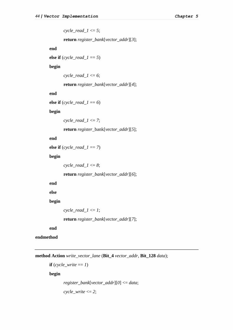
44 | Vector Implementation Chapter 5
cycle_read_1 <= 5;
return register_bank[vector_addr][3];
end
else if (cycle_read_1 == 5)
begin
cycle_read_1 <= 6;
return register_bank[vector_addr][4];
end
else if (cycle_read_1 == 6)
begin
cycle_read_1 <= 7;
return register_bank[vector_addr][5];
end
else if (cycle_read_1 == 7)
begin
cycle_read_1 <= 8;
return register_bank[vector_addr][6];
end
else
begin
cycle_read_1 <= 1;
return register_bank[vector_addr][7];
end
endmethod
method Action write_vector_lane (Bit_4 vector_addr, Bit_128 data);
if (cycle_write == 1)
begin
register_bank[vector_addr][0] <= data;
cycle_write <= 2;

45 | Vector Implementation Chapter 5
end
else if (cycle_write == 2)
begin
register_bank[vector_addr][1] <= data;
cycle_write <= 3;
end
else if (cycle_write == 3)
begin
register_bank[vector_addr][2] <= data;
cycle_write <= 4;
end
else if (cycle_write == 4)
begin
register_bank[vector_addr][3] <= data;
cycle_write <= 5;
end
else if (cycle_write == 5)
begin
register_bank[vector_addr][4] <= data;
cycle_write <= 6;
end
else if (cycle_write == 6)
begin
register_bank[vector_addr][5] <= data;
cycle_write <= 7;
end
else if (cycle_write == 7)
begin
register_bank[vector_addr][6] <= data;
cycle_write <= 8;

46 | Testbench Module – Top Module Chapter 5
end
else
begin
register_bank[vector_addr][7] <= data;
cycle_write <= 1;
end
endmethod
5.2.5 Vector Data Memory Module This module is similar to the Instruction Memory Module and the Data Memory
Module that described in the section of scalar implementation. It is responsible for help-
ing the implementation of the vector load and vector store instructions. It is initialized
by a file; it has two methods for reading and two methods for writing because we may
want to perform two parallel vector loads or two parallel vector stores. Reading meth-
ods get as argument the address of the element that the instruction asks and returns the
element itself. Writing methods are action methods that get the element that the instruc-
tion need to store to memory and the address in which this element will be stored and
stores it.
5.3 Testbench Module – Top Module This module is the main and most important module of the design. It is the place
that every instruction is been executed. It is where every other module’s functions are
called and where the pipeline is been implemented. It is composed out of 8 rules that
fire at different situations. These rules are:
Fetch Rule: This rule is the Fetch Stage of our design. In this rule, we read an
instruction from the instruction memory. The instruction is then being saved to
a pipeline register in order to get into the pipeline.
Decode Rule: This rule is the Decode Stage of our design. In this rule, we make
use of the function on the decode module in order to decode the instruction that
saved in the previous cycle from the fetch rule. Decode rule is actually a transi-
tional rule that decodes the instruction being fetched and passes the appropriate
signals to the appropriate pipeline registers in order to be used in the execution
stages.
Execute Rule: This rule is actually the Execution Stage of the scalar design. In
this rule, first, we check if the scalar instruction can be executed by reading the
cpsr register (conditional execution). If the instruction cannot be executed, then

47 | Testbench Module – Top Module Chapter 5
nothing happens and we move to the following instruction that is on the pipe-
line. If the instruction is able to be executed, then we read the registers that have
been filled from the decode stage and we perform the instruction. An instruction
on the scalar design is being executed through a function for convenience. In
this function, we check the type of the instruction and we perform the proper
steps. For example, if the instruction is a data processing instruction, we read
the operand registers by calling the appropriate methods of the register file mod-
ule; we perform any shift operations needed by calling the function of the barrel
shifter module, given the appropriate arguments; we execute the operation by
calling the function of the ALU module, given the appropriate arguments; we
write the result to the register file and we update the cpsr register if the instruc-
tion demands.
Execute Vector 1 Rule: This rule is actually the Execution Stage of the vector
design. In this rule we check for the type of the instruction (vector data pro-
cessing, vector load/store, vector multiply) and we perform the appropriate steps
just like on the execution rule of the scalar design. The difference between this
rule and the execution rule on the scalar design is that this rule is going to be
called 8 times for a vector instruction, because, as we described in previous
sections, a vector instruction needs 8 cycles in order to be fully executed.
Execute Vector 2 Rule: This rule has the same functionality like the Execute
Vector 1 Rule. It was created in order our processor to be able to execute two
vector instructions simultaneously.
Schedule Instructions Rule: This rule is responsible for the scheduling of the
instructions in the pipeline. As we said before, every vector instruction must
stay into the vector execution stage of the pipeline for 8 cycles in order to be
fully executed, while scalar instructions can be executed in a single cycle.
Therefore, in order to achieve that, we have created three different pipeline reg-
isters for the fetch-to-decode stage that holds three different instructions (2 vec-
tor and 1 scalar). The value of these registers remains the same for 8 cycles (2
extra counters that counts 8 cycles in order the processor to know if a vector
instruction is finished) if we are talking about a vector instruction and changes
in every cycle if we are talking about scalar instructions (1 extra counter that
keeps the processor informed for the scalar instructions). To conclude, this rule
actually decides whether a new instruction is able to be fetched.
Exit Case Rule: This rule is actually the terminal rule of the system. It fires
when we reach a specific amount of cycles, which are given by the designer.
The only job of this rule is to shut down the design.
Increase Cycle Rule: This rule is doing what its name betrays. It increases a
counter that helps to control the pipeline.

48 | Testbench Module – Top Module Chapter 5
Now we are going to explain in detail how our design works when an instruction
is ready to be inserted into the pipeline. The instruction is read in the fetch stage (cycle
0) and is saved to the appropriate pipeline register (instruction). Decode rule then fires
(cycle 1), reads the register that the instruction has been saved before and decodes it.
The outputs of the decode function are saved to the appropriate pipeline registers in
order to be used from the third pipeline stage (Execute Stage). In parallel, a new in-
struction has already been fetched. If the instruction is a scalar one, scalar execution
rule fires (cycle 2) and the execution starts by reading the registers that has been written
in decode stage. If the instruction is a vector one, vector execution rule fires (cycle 2)
and the execution starts by reading the registers that has been written in decode stage.
This rule is going to fire for eight continuous cycles. In parallel a new instruction has
been fetched and the previous new instruction has already been in the decode stage.
This keeps going until all instructions of the program have been executed.
Branch Instructions
If a branch instruction is being fetched into the pipeline then we stall the pipeline in
order to check if the branch will be taken or untaken. If the branch instruction is taken
then the next instruction that is going to be fetched will be in the new value of the pc
register. If the branch instruction is not taken, then the execution continues normally
and we fetch the instruction that is placed after the branch one.

49 | Debugging and Testing Chapter 6
Chapter 6
Debugging and Testing
In this chapter, we are going to describe how the debugging of the project was
done and we will present figures and simulations that confirm the correctness of the
functionality of our design.
6.1 Debugging of the Design
In order to debug the scalar unit of the processor we made use of a highly visual
ARM emulator called VisUAL. VisUAL has been developed as a cross-platform tool
to make learning ARM assembly language easier. In addition to emulating a subset of
the ARM UAL instruction set, it provides visualizations of key concepts unique to as-
sembly language programming and therefore helps make programming ARM assembly
more accessible. It has been designed specifically to use as a teaching tool for the In-
troduction to Computer Architecture course taught at the Department of Electrical and
Electronic Engineering of Imperial College in London.
Some of the key features that this program provides are:
Navigation of Program History: In addition to stepping through code, users
can navigate program history by browsing past register values.
Pointer Visualization: Pointers in ARM assembly can be quite difficult to un-
derstand, especially since ARM assembly has 9 different variations of pointer
behavior when it comes to load/store instructions. VisUAL provides an infor-
mation panel that displays useful pointer information when needed.
Shift Operation Visualization: VisUAL can demonstrate shift operations by
playing them as animations. The animations use actual data values from the shift
instruction being demonstrated.
Memory Access Visualization: All memory access operations, word-aligned
or byte-aligned, can be visualized. Base and offset addresses are shown, and any
values that have been changed are highlighted.

50 | Debugging of the Design Chapter 6
Stack Visualization: Instructions to load/store multiple instructions in the form
of a stack can be visualized. Stack behavior is described, and the stack as well
as stack pointer at the start and end of the stack are displayed.
Branch Visualization: Color-coded line highlights are used to indicate when a
branch is being taken. For conditional instructions, status bits involved in con-
dition checking are highlighted. An arrow points to the branch destination, act-
ing as a visual cue to indicate a branch to another line of code is about to take
place.
Subroutine Visualization: Whenever the link register is set to enter a subrou-
tine, the linked subroutine return point will be highlighted and will remain high-
lighted until the subroutine exits.
Error Correction Suggestions: As opposed to providing cryptic compiler error
messages, VisUAL provides context-specific error messages with explanations
of exactly what is expected. In addition, whenever a runtime error occurs, the
user is informed of the problematic instruction and what operation in the in-
struction resulted in the error.
Infinite Loop Detection: Inadvertently typed code that may result in an infinite
loop can cause code to malfunction. VisUAL detects possible infinite loops and
prompts the user to select the appropriate response.
View Memory Contents: By using the view memory contents window, data
defined in memory can be monitored in real-time as it changes. This allows fast
debugging of memory access instructions from a static viewpoint in addition to
the dynamic viewpoint provided by the pointer and memory access visualiza-
tions.
View Symbols: The symbols window provides a list of all code and data sym-
bols that have been defined. This provides an easy method of lookup up symbols
during execution.
Headless Emulation Mode: VisUAL allows assembly code to be executed via
the command line and logs the program state to an XML file. This is useful for
power users for testing large batches of code.
The main characteristic that we fully took advantage of VisUAL was the real-
time and step-by-step execution of an ARM assembly code. Executing a code step-
by-step made easy to check what values the registers and the memory should have
at any time of the progress. Therefore, by observing our simulation we could easily
check if our registers, memory, results on the ALU or Barrel Shifter, etc. was getting
the right values.

51 | Testing the Scalar Unit Chapter 6
As it concerns the vector unit of our processor, we did not make use of any
emulator. The debugging of this unit has been done “by-hand”. This means that we
manually inserted every combination of instructions and observed the simulations
for the correctness of the functionality of our design.
6.2 Testing the Scalar Unit
In order to test our scalar design, at first, we used some written by-hand instruc-
tions. Then, and since this method is not the most efficient, for the verification of our
design, we used real programs written in C++.
Nevertheless, processors does not read and execute C++ programs. They can
read instructions written on a binary or a hexadecimal form. So in order to achieve that
we first should translate the C++ programs into ARM assembly. The translation to as-
sembly was done via the ARM GCC 6.3.0 and by making use of the online tool
https://gcc.godbolt.org/. In this tool, we should select ARM gcc 6.3.0 and put the fol-
lowing flags as compiler options:
1. fomit-frame-pointer
2. –mcpu=arm7tdmi
The first flag asks the tool not to use the frame pointer while creating the assembly
instructions and the second one specifies the target device. In continue, the assembly
code is saved on a .s file.
At this point, we needed to translate and transform the ARM assembly code,
that we saved in the .s file, to files with binaries or hexadecimal instructions. To achieve
that, we made use of the GNU ARM Embedded Toolchain by writing the following
commands on the terminal:
1. arm-none-eabi-as -EB -o example.o example.s
2. arm-none-eabi-ld -EB -Ttext=0x0 -o example.elf example.o
3. arm-none-eabi-objcopy -O binary example.elf example.bin
The first command assembles the .s file that we previously created. The second
calls the linker of GNU Toolchain. The –Ttext=0x0 specifies that addresses should be
assigned to the labels, such that the instructions were starting from address 0x0. Finally,
the third one produces the .bin file, which is the assembly commands in a hexadecimal
format.
In the upcoming subsections we will provide every test that our scalar unit
passed as long as the codes with whom our processor was fed and the simulation that it
created.

52 | Testing the Scalar Unit Chapter 6
6.2.1 “By-hand” Testing Example The first example that our scalar unit passed successfully was some manually
given binary instructions. Below we provide these binary instructions as long as the
simulation that our scalar unit produced:
Figure 6. 1: Binary Instructions of the “By-Hand” Example
After every binary instruction, we provide some comments of what actions the instruc-
tion is going to do and what results we expect.
Figure 6. 2: VCD Output of the “By-Hand” Example
Figure 6.2 presents the waveform results of the Figure’s 6.1 instructions. As we can
observe, the registers take the exact values with the ones that we expected.

53 | Testing the Scalar Unit Chapter 6
6.2.2 Factorial Testing Example This is the first real program that our scalar processor passed successfully. It is
about a factorial count calculation of a specific number. In this case, this specific num-
ber is the number 8. The factorial of eight is: 8! = 1x2x3x4x5x6x7x8 = 40,320. There-
fore, we expect this number to be stored to a register of our scalar register bank. Below
we provide the C++ and the assembly codes, exactly like the tools that we mentioned
above translated them for us.
Figure 6. 3: C++ Code of the Factorial Example
Figure 6.4: Assembly Code of the Factorial Example

54 | Testing the Scalar Unit Chapter 6
As we can observe from the assembly code, the solution number is expected to
be stored in register R3. After that, R3’s value is expected to become zero and finally
stack pointer’s value will be restored to its initial value (100).
Below we provide the VCD output that came up after running the above pro-
grams to our processor:
Figure 6. 5: VCD Output of the Factorial Example
Indeed, observing the VCD output, we can confirm that register R3 took the
correct result, then its value became zero and finally the stack pointer (R14) get its
initial value.
6.2.3 Largest Number Among Three (LNA3) Testing Example Another program that tested the functionality of the processor was Larger Num-
ber Among 3. This program takes three numbers as inputs, compares them and decides
what number is the biggest one. Below we provide the C++ and the assembly codes of
this program:
Figure 6. 6: C++ Code of the Largest Number Among Three Example

55 | Testing the Scalar Unit Chapter 6
Figure 6. 7: Assembly Code of the Largest Number Among Three Example
Below we are going to provide the VCD output that came up when running the
above programs. We expect to see that comparing 3, 21 and 99, the processor will de-
cide that 99 is the largest value.
Figure 6. 8: VCD Output of the Largest Number Among Three Example
Indeed, we can observe that at first stack pointer is initialized at 100. Then the
three numbers are kept in the stack and comparisons are made between them. Finally,
the largest number (99) is stored to R3. In the end, R3’s value becomes zero and the
stack pointer is restored back to its initial value.

56 | Testing the Scalar Unit Chapter 6
6.2.4 Fibonacci Testing Example The next program, that the processor was tested, was the Fibonacci sequence.
In mathematics, the Fibonacci sequence is characterized by the fact that every number
after the first two is the sum of the two preceding ones. The Fibonacci numbers are the
numbers in the following integer sequence:
1, 1, 2, 3, 5, 8, 13, 21, 34, 55, 89, 144…
The program tests the processor to produce the Fibonacci sequence up to n num-
ber of terms. In this case n = 15 so the expected sequence is:
1, 1, 2, 3, 5, 8, 13, 21, 34, 55, 89, 144, 233, 377.
Below we provide the C++ and the assembly codes of this program:
Figure 6. 9: C++ Code of the Fibonacci Example

57 | Testing the Scalar Unit Chapter 6
Figure 6. 10: Assembly Code of the Fibonacci Example
Below we provide the VCD output that was produced by running the above
codes to the processor. We are expecting to see the number 377 at the 15th term of the
sequence:
Figure 6. 11: VCD Output of the Fibonacci Example

58 | Testing the Scalar Unit Chapter 6
Just as we expected, the 15th term of the Fibonacci sequence is stored in the
register R3. Finally, R3’s value becomes zero and stack pointer returns to its initial
value, which is 100.
6.2.5 Bubblesort Testing Example The last, and most difficult, test, that our processor successfully passed, was the
classic Bubblesort program. This program gets seven values as inputs, and stores them
in an array of integers. After that, a void function is called that sorts these seven values
by comparing and transposing each other. Finally, the values of the array are stored into
different variables for convenience. Below we provide the C++ and the assembly codes
of this example program:
Figure 6. 12: C++ Code of the Bubblesort Example

59 | Testing the Scalar Unit Chapter 6
Figure 6. 13: Assembly Code of the Bubblesort Example
Bellow we provide the VCD output that was produced after running the above programs
to our scalar design. According to the C++ code, values 64, 34, 25, 12, 22, 11 and 90
are inserted into an array of integers. In the end, we expect to see these values to be
sorted in ascending order i.e. 11, 12, 22, 25, 34, 64, 90.

60 | Testing the Vector Unit Chapter 6
Figure 6. 14: VCD Output of the Bubblesort Example
Indeed, by observing the simulations above, we can confirm that initially the
processor stores the right values in the register R3 and in the end of the program R3
gets these values sorted in an ascending order. After that, R3’s value becomes zero and
the stack pointer is restored to its initial value.
6.3 Testing the Vector Unit
In order to test our vector design, we created some written “by-hand” examples.
In these examples, we tested every possible combination and situation of the vector
instructions. We separately tested vector processing instructions, vector multiply and
vector multiply-accumulate instructions as long as vector load and vector store instruc-
tions. In addition, in these examples we checked the parallelization of our design and
by that we mean that two vector instructions can be executed simultaneously and along-
side with scalar ones. In the next subsections, we will provide analytical figures and
simulations of the binary instructions that we filled the processor with, as long as the
VDC outputs that our vector processing unit produced.

61 | Testing the Vector Unit Chapter 6
6.3.1 Parallelization Example This is about a very simple example on our vector processing unit. It is a test
program with just two vector instructions (VMOV) just to check that our vector unit is
able to execute them simultaneously. Below we provide the instructions in a binary
form as long as the VCD output that our processor produced after executing them.
Figure 6. 15: Binary Instructions of the Parallelization Example
Figure 6. 16: VCD Output of the Parallelization Example
As we can observe from the simulation above, there are two vector instructions
running simultaneously with one cycle delay between them. That is because we fetch
one instruction at a time so when we fetched the first vector instruction, we inserted it
into the pipeline and one cycle later we were able to fetch the other vector instruction
because our second vector functional unit was free. Thus, we can see that value 15 is
written cycle-by-cycle in every element of the first vector register as long as value 10
is written cycle-by-cycle in every element of the second vector register.
6.3.2 Vector Multiply Example This is about a little more complicated example than the one before. It is a test
program with some vector instructions (vector data processing, vector multiply and
vector multiply with accumulation) in order to check the functionality of our design.
Below we introduce the instructions in binary form, as long as the VCD output of our
processor.
Figure 6. 17: Binary Instructions of the Vector Multiply Example

62 | Testing the Vector Unit Chapter 6
Figure 6. 18: VCD Output of the Vector Multiply Example
In the simulation above, we can confirm the functionality of our design. Indeed,
at first, two vector move instructions are executed and fill the elements of vector register
0 and vector register 1 with the appropriate values (15 and 10). After that the vector add
instruction alongside with the vector multiply instruction are executed and produce the
correct results on vector register 3 and vector register 4. Finally, a vector multiply and
accumulate instruction is executed and produces the appropriate results on the vector
register 1.
The results on the vector registers are in hexadecimal format for convenience.

63 | Testing the Vector Unit Chapter 6
6.3.3 Vector Load and Vector Store Example This is a similar test program like the one before, only that now it contains vec-
tor data processing instructions as long as vector load and vector store instructions. It
is created in order to check the functionality of the vector load and vector store instruc-
tions. The instructions in binary form as long as the VCD output that the processor
produced after running these instructions are provided below:
Figure 6. 19: Binary Instructions of the Vector Load and Vector Store Example

64 | Testing the Vector Unit Chapter 6
Figure 6. 20: VCD Output of the Vector Load and Vector Store Example
As we can observe from the simulation above, it is confirmed that our vector
processing unit passes with success this test program too. Indeed, at first, there are two
scalar move instructions that are executed in order to help the execution of the upcom-
ing vector instructions. Alongside with the scalar ones, two vector instructions are ex-
ecuted simultaneously and produce the appropriate results on the vector registers 0 and
1. After that, a vector add instruction and a vector store instruction are executed in
parallel and produce the correct results on vector register 3 and on memory. To fully-
test the vector store instruction, we finally execute a vector load one at the exact
memory positions the vector store instruction was executed. The results are the ex-
pected ones, thus we conclude that these instructions are also been executed correctly.
6.3.4 Multiple Scalar & Vector Instructions Example
This is about one of the most complicated programs that we tested on our pro-
cessor. It is about many written “by-hand” instructions that test the vector and scalar
part separately and alongside. For convenience, we will only provide the program as it
concerns the instructions in binary form. The VCD outputs can be tested by executing
this test program. It is not provided here because it is quite a waste of space.
The binary instructions are introduced in the figure below:

65 | Design Evaluation Chapter 6
Figure 6. 21: Binary Instructions of the Multiple Scalar and Vector Instructions Example
6.4 Design Evaluation
In this section, we are going to introduce our design’s utilization after only syn-
thesizing it on Xilinx ISE 14.7 tool with the use of a board, which is on the Artix – 7
family. After that, we are going to compare our scalar design only with Piccolo and
LEON2 processors and make annotations on the results.
Below we introduce the utilization of our design (Vector & Scalar) after synthesizing
it on the FPGA board we mentioned before. It is crucial to point out that the results
below are not taken after Place & Rout but only in synthesizing level:
Slice Registers Slice LUTs DSPs
~=15.500 ~=250.000 ~=150
The conclusion is that these numbers, of course, are not the optimal ones. The
sure thing is that our design can have several to many improvements as far as it concerns
the clock frequency and the use of resources in the FPGA. In this place, however, it is
good to be mentioned that it was the first time that this type of tools and language (BSV)
was used for such designs. It is also worth to be mentioned that our vector design is a

66 | Design Evaluation Chapter 6
really wide unit that can hold up to 15 1024-bit quantities in each vector register bank,
as long as it can execute two vector instructions simultaneously.
Below we introduce the utilization of our scalar design only after synthesizing it on the
FPGA board we mentioned before:
Slice Registers Slice LUTs
~=680 ~=5700
LEON
LEON2 is a 32-bit RISC SPARC V8 compliant architecture, which uses big endian
byte ordering as specified in the SPARC V8 reference manual. LEON2 is a synthesiz-
able processor developed by ESA and maintained by Gaisler Research. The processor
was originally developed as a fault-tolerant processor for space applications. This report
covers the non-fault-tolerant version licensed under the GNU LGPL license, which is
freely available as a VHDL model from the Gaisler Research website. LEON2 targets
both the ASIC and FPGA markets.
Piccolo
Piccolo is a 32-bit processor implemented by Bluespec Inc. The architecture of this
processor is based on the RV32IM ISA. Some features of the free version are:
100MHz
3-stage pipeline
<3000 LUTs
Below we introduce an overview of the three processors’ designs (LEON, Piccolo and
our scalar design):
Pipeline Stages LUTs
LEON2 5-stage 3820-7178
Piccolo 3-stage <3000
Our Scalar Design 3-stage 5700
As we can observe, our scalar design has comparable results with the other two proces-
sors. However, by studying those results, we can conclude that the optimization of our
design is feasible.

67 | Conclusion Chapter 7
Chapter 7
Conclusion
7.1 Conclusion of Thesis
This thesis was an attempt to implement an ARM processor with SIMD exten-
sions in Bluespec System Verilog Hardware Description Language. It was a challenge
for us to study the ARM architecture, learn about Vector processors and finally get
experienced with a new HDL, the Bluespec language. After experimenting with the
BSV, it is easy for us to conclude that this HDL is suitable for this kind of work. The
implementation of any processor in BSV is easier and this is because Bluespec is more
like High Level languages, which are used for software development (C++ , Java), ra-
ther than other HDLs (Verilog, VHDL). It also provides the ability to design circuits in
a more detailed and targeted way.
7.2 Future Work
Code optimization for higher clock frequency and fewer resources on the FPGA
Expand the Pipeline Stages
Forwarding and Chaining Optimizations after expanding the pipeline stages or
inserting other type of instructions
Instruction and Data Caches
Expand the instruction set to another version.
More experience with the tool to find an optimal way to design a processor on
it.
Power management of the design

68 | Bibliography Chapter 8
Bibliography
1. “Bluespec TM System Verilog Reference Guide” Revision: 30 July 2014
2. Rishiyur S. Nikhil and Kathy R. Czeck, “BSV by Example” 2010
3. ARM Architecture Reference Manual
4. ARM7TDMI Reference Manual
5. “Ψηφιακοί Υπολογιστές” Lectures ARM ISA
6. Arvind, Rishiyur S. Nikhil, Joel S. Emer 3, Murali Vijayaraghavan: “Computer
Architecture: A Constructive Approach Using Executable and Synthesizable
Specifications” December 2012
7. Nirav Hemant Dave, “Designing a Processor in Bluespec”, January 2005
8. http://wiki.bluespec.com/
9. http://infocenter.arm.com/
10. http://cva.stanford.edu/classes/ee482s/scribed/lect11.pdf
11. https://www.ece.cmu.edu/~ece740/f13/lib/exe/fetch.php%3Fmedia%3Dseth-
740-fall13-module5.1-simd-vector-gpu.pdf
12. https://community.arm.com/processors/b/blog/posts/coding-for-neon---part-1-
load-and-stores
13. https://salmanarif.bitbucket.io/visual/index.html
14. http://www.davespace.co.uk/arm/introduction-to-arm/

69 | Bibliography Chapter 8
15. https://en.wikipedia.org/wiki/SIMD
16. https://en.wikipedia.org/wiki/Vector_processor
17. https://www.youtube.com/channel/UCCCz-aX7zzowKXyhKGsTx1Q
18. http://aelmahmoudy.users.sourceforge.net/electronix/arm/
19. https://www.youtube.com/watch?v=8dljs0wt4V4