Embed Size (px)
Citation preview
Qucs
Technical Papers
Stefan JahnMichael Margraf
Vincent HabchiRaimund Jacob
Copyright c© 2003, 2004, 2005, 2006, 2007 Stefan Jahn <[email protected]>Copyright c© 2003, 2004, 2005, 2006, 2007 Michael Margraf <[email protected]>Copyright c© 2004, 2005 Vincent Habchi, F5RCS <[email protected]>Copyright c© 2005 Raimund Jacob <[email protected]>
Permission is granted to copy, distribute and/or modify this document under the terms of the GNU FreeDocumentation License, Version 1.1 or any later version published by the Free Software Foundation. Acopy of the license is included in the section entitled ”GNU Free Documentation License”.
Contents
1 Scattering parameters 61.1 Introduction and definition . . . . . . . . . . . . . . . . . . . . . . . . . . . . . . . . . . 61.2 Waves on Transmission Lines . . . . . . . . . . . . . . . . . . . . . . . . . . . . . . . . . 61.3 Computing with S-parameters . . . . . . . . . . . . . . . . . . . . . . . . . . . . . . . . 8
1.3.1 S-parameters in CAE programs . . . . . . . . . . . . . . . . . . . . . . . . . . . 81.3.2 Differential S-parameter ports . . . . . . . . . . . . . . . . . . . . . . . . . . . . 12
1.4 Applications . . . . . . . . . . . . . . . . . . . . . . . . . . . . . . . . . . . . . . . . . . 131.4.1 Stability . . . . . . . . . . . . . . . . . . . . . . . . . . . . . . . . . . . . . . . . 131.4.2 Gain . . . . . . . . . . . . . . . . . . . . . . . . . . . . . . . . . . . . . . . . . . 151.4.3 Two-Port Matching . . . . . . . . . . . . . . . . . . . . . . . . . . . . . . . . . . 16
2 Noise Waves 172.1 Definition . . . . . . . . . . . . . . . . . . . . . . . . . . . . . . . . . . . . . . . . . . . 172.2 Noise Parameters . . . . . . . . . . . . . . . . . . . . . . . . . . . . . . . . . . . . . . . 182.3 Noise Wave Correlation Matrix in CAE . . . . . . . . . . . . . . . . . . . . . . . . . . . 192.4 Noise Correlation Matrix Transformations . . . . . . . . . . . . . . . . . . . . . . . . . . 22
2.4.1 Forming the noise current correlation matrix . . . . . . . . . . . . . . . . . . . . 232.4.2 Transformations . . . . . . . . . . . . . . . . . . . . . . . . . . . . . . . . . . . 23
2.5 Noise Wave Correlation Matrix of Components . . . . . . . . . . . . . . . . . . . . . . . 24
3 DC Analysis 253.1 Modified Nodal Analysis . . . . . . . . . . . . . . . . . . . . . . . . . . . . . . . . . . . 25
3.1.1 Generating the MNA matrices . . . . . . . . . . . . . . . . . . . . . . . . . . . . 263.1.2 The A matrix . . . . . . . . . . . . . . . . . . . . . . . . . . . . . . . . . . . . . 263.1.3 The x matrix . . . . . . . . . . . . . . . . . . . . . . . . . . . . . . . . . . . . . 273.1.4 The z matrix . . . . . . . . . . . . . . . . . . . . . . . . . . . . . . . . . . . . . 283.1.5 A simple example . . . . . . . . . . . . . . . . . . . . . . . . . . . . . . . . . . 28
3.2 Extensions to the MNA . . . . . . . . . . . . . . . . . . . . . . . . . . . . . . . . . . . . 303.3 Non-linear DC Analysis . . . . . . . . . . . . . . . . . . . . . . . . . . . . . . . . . . . 31
3.3.1 Newton-Raphson method . . . . . . . . . . . . . . . . . . . . . . . . . . . . . . . 313.3.2 Convergence . . . . . . . . . . . . . . . . . . . . . . . . . . . . . . . . . . . . . 34
3.4 Overall solution algorithm for DC Analysis . . . . . . . . . . . . . . . . . . . . . . . . . 36
4 AC Analysis 39
5 AC Noise Analysis 405.1 Definitions . . . . . . . . . . . . . . . . . . . . . . . . . . . . . . . . . . . . . . . . . . . 405.2 The Algorithm . . . . . . . . . . . . . . . . . . . . . . . . . . . . . . . . . . . . . . . . 40
5.2.1 A Simple Example . . . . . . . . . . . . . . . . . . . . . . . . . . . . . . . . . . 425.3 Noise Current Correlation Matrix . . . . . . . . . . . . . . . . . . . . . . . . . . . . . . . 43
1
6 Transient Analysis 446.1 Integration methods . . . . . . . . . . . . . . . . . . . . . . . . . . . . . . . . . . . . . . 44
6.1.1 Properties of numerical integration methods . . . . . . . . . . . . . . . . . . . . . 456.1.2 Elementary Methods . . . . . . . . . . . . . . . . . . . . . . . . . . . . . . . . . 456.1.3 Linear Multistep Methods . . . . . . . . . . . . . . . . . . . . . . . . . . . . . . 466.1.4 Stability considerations . . . . . . . . . . . . . . . . . . . . . . . . . . . . . . . . 48
6.2 Predictor-corrector methods . . . . . . . . . . . . . . . . . . . . . . . . . . . . . . . . . 516.2.1 Order and local truncation error . . . . . . . . . . . . . . . . . . . . . . . . . . . 516.2.2 Milne’s estimate . . . . . . . . . . . . . . . . . . . . . . . . . . . . . . . . . . . 536.2.3 Adaptive step-size control . . . . . . . . . . . . . . . . . . . . . . . . . . . . . . 53
6.3 Energy-storage components . . . . . . . . . . . . . . . . . . . . . . . . . . . . . . . . . . 546.3.1 Capacitor . . . . . . . . . . . . . . . . . . . . . . . . . . . . . . . . . . . . . . . 546.3.2 Inductor . . . . . . . . . . . . . . . . . . . . . . . . . . . . . . . . . . . . . . . . 556.3.3 Coupled Inductors . . . . . . . . . . . . . . . . . . . . . . . . . . . . . . . . . . 566.3.4 Depletion Capacitance . . . . . . . . . . . . . . . . . . . . . . . . . . . . . . . . 576.3.5 Diffusion Capacitance . . . . . . . . . . . . . . . . . . . . . . . . . . . . . . . . 586.3.6 MOS Gate Capacitances . . . . . . . . . . . . . . . . . . . . . . . . . . . . . . . 58
6.4 Special time-domain models . . . . . . . . . . . . . . . . . . . . . . . . . . . . . . . . . 596.4.1 AM modulated AC source . . . . . . . . . . . . . . . . . . . . . . . . . . . . . . 596.4.2 PM modulated AC source . . . . . . . . . . . . . . . . . . . . . . . . . . . . . . 59
6.5 Components defined in the frequency domain . . . . . . . . . . . . . . . . . . . . . . . . 606.5.1 Components with frequency-independent delay times . . . . . . . . . . . . . . . . 606.5.2 Components with frequency-dependent delay times and losses . . . . . . . . . . . 65
6.6 Convergence . . . . . . . . . . . . . . . . . . . . . . . . . . . . . . . . . . . . . . . . . 676.6.1 Limiting schemes . . . . . . . . . . . . . . . . . . . . . . . . . . . . . . . . . . . 676.6.2 Continuation schemes . . . . . . . . . . . . . . . . . . . . . . . . . . . . . . . . 68
7 Harmonic Balance Analysis 697.1 The Basic Concept . . . . . . . . . . . . . . . . . . . . . . . . . . . . . . . . . . . . . . 697.2 Going through each Step . . . . . . . . . . . . . . . . . . . . . . . . . . . . . . . . . . . 71
7.2.1 Creating Transadmittance Matrix . . . . . . . . . . . . . . . . . . . . . . . . . . 717.2.2 Starting Values . . . . . . . . . . . . . . . . . . . . . . . . . . . . . . . . . . . . 727.2.3 Solution algorithm . . . . . . . . . . . . . . . . . . . . . . . . . . . . . . . . . . 727.2.4 Termination Criteria . . . . . . . . . . . . . . . . . . . . . . . . . . . . . . . . . 74
7.3 A Symbolic HB Algorithm . . . . . . . . . . . . . . . . . . . . . . . . . . . . . . . . . . 747.4 Large-Signal S-Parameter Simulation . . . . . . . . . . . . . . . . . . . . . . . . . . . . 747.5 Autonomous Harmonic Balance . . . . . . . . . . . . . . . . . . . . . . . . . . . . . . . 75
8 Harmonic Balance Noise Analysis 768.1 The Linear Subcircuit . . . . . . . . . . . . . . . . . . . . . . . . . . . . . . . . . . . . . 768.2 The Non-Linear Subcircuit . . . . . . . . . . . . . . . . . . . . . . . . . . . . . . . . . . 778.3 Noise Conversion . . . . . . . . . . . . . . . . . . . . . . . . . . . . . . . . . . . . . . . 778.4 Phase and Amplitude Noise . . . . . . . . . . . . . . . . . . . . . . . . . . . . . . . . . . 78
9 Linear devices 799.1 Resistor . . . . . . . . . . . . . . . . . . . . . . . . . . . . . . . . . . . . . . . . . . . . 799.2 Capacitor . . . . . . . . . . . . . . . . . . . . . . . . . . . . . . . . . . . . . . . . . . . 809.3 Inductor . . . . . . . . . . . . . . . . . . . . . . . . . . . . . . . . . . . . . . . . . . . . 809.4 DC Block . . . . . . . . . . . . . . . . . . . . . . . . . . . . . . . . . . . . . . . . . . . 819.5 DC Feed . . . . . . . . . . . . . . . . . . . . . . . . . . . . . . . . . . . . . . . . . . . . 819.6 Bias T . . . . . . . . . . . . . . . . . . . . . . . . . . . . . . . . . . . . . . . . . . . . . 819.7 Transformer . . . . . . . . . . . . . . . . . . . . . . . . . . . . . . . . . . . . . . . . . . 829.8 Symmetrical transformer . . . . . . . . . . . . . . . . . . . . . . . . . . . . . . . . . . . 839.9 Non-ideal transformer . . . . . . . . . . . . . . . . . . . . . . . . . . . . . . . . . . . . . 84
2
9.9.1 Mutual inductors with two or three of inductors . . . . . . . . . . . . . . . . . . . 849.9.2 Mutual inductors with any number of inductors . . . . . . . . . . . . . . . . . . . 86
9.10 Attenuator . . . . . . . . . . . . . . . . . . . . . . . . . . . . . . . . . . . . . . . . . . . 879.11 Amplifier . . . . . . . . . . . . . . . . . . . . . . . . . . . . . . . . . . . . . . . . . . . 879.12 Isolator . . . . . . . . . . . . . . . . . . . . . . . . . . . . . . . . . . . . . . . . . . . . 889.13 Circulator . . . . . . . . . . . . . . . . . . . . . . . . . . . . . . . . . . . . . . . . . . . 899.14 Phase shifter . . . . . . . . . . . . . . . . . . . . . . . . . . . . . . . . . . . . . . . . . . 899.15 Coupler . . . . . . . . . . . . . . . . . . . . . . . . . . . . . . . . . . . . . . . . . . . . 909.16 Gyrator . . . . . . . . . . . . . . . . . . . . . . . . . . . . . . . . . . . . . . . . . . . . 919.17 Voltage and current sources . . . . . . . . . . . . . . . . . . . . . . . . . . . . . . . . . . 929.18 Noise sources . . . . . . . . . . . . . . . . . . . . . . . . . . . . . . . . . . . . . . . . . 93
9.18.1 Noise current source . . . . . . . . . . . . . . . . . . . . . . . . . . . . . . . . . 939.18.2 Noise voltage source . . . . . . . . . . . . . . . . . . . . . . . . . . . . . . . . . 939.18.3 Correlated noise sources . . . . . . . . . . . . . . . . . . . . . . . . . . . . . . . 94
9.19 Controlled sources . . . . . . . . . . . . . . . . . . . . . . . . . . . . . . . . . . . . . . 969.19.1 Voltage controlled current source . . . . . . . . . . . . . . . . . . . . . . . . . . 969.19.2 Current controlled current source . . . . . . . . . . . . . . . . . . . . . . . . . . 979.19.3 Voltage controlled voltage source . . . . . . . . . . . . . . . . . . . . . . . . . . 979.19.4 Current controlled voltage source . . . . . . . . . . . . . . . . . . . . . . . . . . 98
9.20 Transmission Line . . . . . . . . . . . . . . . . . . . . . . . . . . . . . . . . . . . . . . . 999.21 Differential Transmission Line . . . . . . . . . . . . . . . . . . . . . . . . . . . . . . . . 1009.22 Coupled transmission line . . . . . . . . . . . . . . . . . . . . . . . . . . . . . . . . . . . 1019.23 S-parameter container with additional reference port . . . . . . . . . . . . . . . . . . . . 1029.24 Real-Life Models . . . . . . . . . . . . . . . . . . . . . . . . . . . . . . . . . . . . . . . 103
10 Non-linear devices 10510.1 Operational amplifier . . . . . . . . . . . . . . . . . . . . . . . . . . . . . . . . . . . . . 10510.2 PN-Junction Diode . . . . . . . . . . . . . . . . . . . . . . . . . . . . . . . . . . . . . . 106
10.2.1 Large signal model . . . . . . . . . . . . . . . . . . . . . . . . . . . . . . . . . . 10710.2.2 Small signal model . . . . . . . . . . . . . . . . . . . . . . . . . . . . . . . . . . 10810.2.3 Noise model . . . . . . . . . . . . . . . . . . . . . . . . . . . . . . . . . . . . . 10810.2.4 Temperature model . . . . . . . . . . . . . . . . . . . . . . . . . . . . . . . . . . 11010.2.5 Area dependence of the model . . . . . . . . . . . . . . . . . . . . . . . . . . . . 111
10.3 Junction FET . . . . . . . . . . . . . . . . . . . . . . . . . . . . . . . . . . . . . . . . . 11110.3.1 Large signal model . . . . . . . . . . . . . . . . . . . . . . . . . . . . . . . . . . 11110.3.2 Small signal model . . . . . . . . . . . . . . . . . . . . . . . . . . . . . . . . . . 11410.3.3 Noise model . . . . . . . . . . . . . . . . . . . . . . . . . . . . . . . . . . . . . 11510.3.4 Temperature model . . . . . . . . . . . . . . . . . . . . . . . . . . . . . . . . . . 11610.3.5 Area dependence of the model . . . . . . . . . . . . . . . . . . . . . . . . . . . . 117
10.4 Homo-Junction Bipolar Transistor . . . . . . . . . . . . . . . . . . . . . . . . . . . . . . 11710.4.1 Large signal model . . . . . . . . . . . . . . . . . . . . . . . . . . . . . . . . . . 11810.4.2 Small signal model . . . . . . . . . . . . . . . . . . . . . . . . . . . . . . . . . . 12310.4.3 Noise model . . . . . . . . . . . . . . . . . . . . . . . . . . . . . . . . . . . . . 12510.4.4 Temperature model . . . . . . . . . . . . . . . . . . . . . . . . . . . . . . . . . . 12610.4.5 Area dependence of the model . . . . . . . . . . . . . . . . . . . . . . . . . . . . 127
10.5 MOS Field-Effect Transistor . . . . . . . . . . . . . . . . . . . . . . . . . . . . . . . . . 12810.5.1 Large signal model . . . . . . . . . . . . . . . . . . . . . . . . . . . . . . . . . . 13010.5.2 Physical model . . . . . . . . . . . . . . . . . . . . . . . . . . . . . . . . . . . . 13310.5.3 Small signal model . . . . . . . . . . . . . . . . . . . . . . . . . . . . . . . . . . 13510.5.4 Noise model . . . . . . . . . . . . . . . . . . . . . . . . . . . . . . . . . . . . . 13810.5.5 Temperature model . . . . . . . . . . . . . . . . . . . . . . . . . . . . . . . . . . 139
10.6 Models for boolean devices . . . . . . . . . . . . . . . . . . . . . . . . . . . . . . . . . . 14010.7 Equation defined models . . . . . . . . . . . . . . . . . . . . . . . . . . . . . . . . . . . 141
10.7.1 Models with Explicit Equations . . . . . . . . . . . . . . . . . . . . . . . . . . . 142
3
10.7.2 Models with Implicit Equations . . . . . . . . . . . . . . . . . . . . . . . . . . . 143
11 Microstrip components 14611.1 Single microstrip line . . . . . . . . . . . . . . . . . . . . . . . . . . . . . . . . . . . . . 146
11.1.1 Quasi-static characteristic impedance . . . . . . . . . . . . . . . . . . . . . . . . 14611.1.2 Quasi-static effective dielectric constant . . . . . . . . . . . . . . . . . . . . . . . 14811.1.3 Strip thickness correction . . . . . . . . . . . . . . . . . . . . . . . . . . . . . . . 14911.1.4 Dispersion . . . . . . . . . . . . . . . . . . . . . . . . . . . . . . . . . . . . . . 15011.1.5 Transmission losses . . . . . . . . . . . . . . . . . . . . . . . . . . . . . . . . . . 155
11.2 Microstrip corner . . . . . . . . . . . . . . . . . . . . . . . . . . . . . . . . . . . . . . . 15611.3 Parallel coupled microstrip lines . . . . . . . . . . . . . . . . . . . . . . . . . . . . . . . 157
11.3.1 Characteristic impedance and effective dielectric constant . . . . . . . . . . . . . 15711.3.2 Strip thickness correction . . . . . . . . . . . . . . . . . . . . . . . . . . . . . . . 16411.3.3 Transmission losses . . . . . . . . . . . . . . . . . . . . . . . . . . . . . . . . . . 164
11.4 Microstrip open . . . . . . . . . . . . . . . . . . . . . . . . . . . . . . . . . . . . . . . . 16511.5 Microstrip gap . . . . . . . . . . . . . . . . . . . . . . . . . . . . . . . . . . . . . . . . . 16511.6 Microstrip impedance step . . . . . . . . . . . . . . . . . . . . . . . . . . . . . . . . . . 16711.7 Microstrip tee junction . . . . . . . . . . . . . . . . . . . . . . . . . . . . . . . . . . . . 16711.8 Microstrip cross . . . . . . . . . . . . . . . . . . . . . . . . . . . . . . . . . . . . . . . . 17011.9 Microstrip via hole . . . . . . . . . . . . . . . . . . . . . . . . . . . . . . . . . . . . . . 17111.10Bondwire . . . . . . . . . . . . . . . . . . . . . . . . . . . . . . . . . . . . . . . . . . . 172
11.10.1 Freespace model . . . . . . . . . . . . . . . . . . . . . . . . . . . . . . . . . . . 17311.10.2 Mirror model . . . . . . . . . . . . . . . . . . . . . . . . . . . . . . . . . . . . . 173
12 Coplanar components 17412.1 Coplanar waveguides (CPW) . . . . . . . . . . . . . . . . . . . . . . . . . . . . . . . . . 174
12.1.1 Definition . . . . . . . . . . . . . . . . . . . . . . . . . . . . . . . . . . . . . . . 17412.1.2 Quasi-static analysis by conformal mappings . . . . . . . . . . . . . . . . . . . . 17512.1.3 Effects of metalization thickness . . . . . . . . . . . . . . . . . . . . . . . . . . . 17812.1.4 Effects of dispersion . . . . . . . . . . . . . . . . . . . . . . . . . . . . . . . . . 17812.1.5 Evaluation of losses . . . . . . . . . . . . . . . . . . . . . . . . . . . . . . . . . 17912.1.6 S- and Y-parameters of the single coplanar line . . . . . . . . . . . . . . . . . . . 179
12.2 Coplanar waveguide open . . . . . . . . . . . . . . . . . . . . . . . . . . . . . . . . . . . 17912.3 Coplanar waveguide short . . . . . . . . . . . . . . . . . . . . . . . . . . . . . . . . . . . 18012.4 Coplanar waveguide gap . . . . . . . . . . . . . . . . . . . . . . . . . . . . . . . . . . . 18012.5 Coplanar waveguide step . . . . . . . . . . . . . . . . . . . . . . . . . . . . . . . . . . . 181
13 Other types of transmission lines 18313.1 Coaxial cable . . . . . . . . . . . . . . . . . . . . . . . . . . . . . . . . . . . . . . . . . 183
13.1.1 Characteristic impedance . . . . . . . . . . . . . . . . . . . . . . . . . . . . . . . 18313.1.2 Losses . . . . . . . . . . . . . . . . . . . . . . . . . . . . . . . . . . . . . . . . . 18313.1.3 Cutoff frequencies . . . . . . . . . . . . . . . . . . . . . . . . . . . . . . . . . . 184
13.2 Twisted pair . . . . . . . . . . . . . . . . . . . . . . . . . . . . . . . . . . . . . . . . . . 18413.2.1 Quasi-static model . . . . . . . . . . . . . . . . . . . . . . . . . . . . . . . . . . 18413.2.2 Transmission losses . . . . . . . . . . . . . . . . . . . . . . . . . . . . . . . . . . 185
14 Synthesizing circuits 18714.1 Attenuators . . . . . . . . . . . . . . . . . . . . . . . . . . . . . . . . . . . . . . . . . . 18714.2 Filters . . . . . . . . . . . . . . . . . . . . . . . . . . . . . . . . . . . . . . . . . . . . . 188
14.2.1 LC ladder filters . . . . . . . . . . . . . . . . . . . . . . . . . . . . . . . . . . . 189
4
15 Mathematical background 19115.1 N-port matrix conversions . . . . . . . . . . . . . . . . . . . . . . . . . . . . . . . . . . 191
15.1.1 Renormalization of S-parameters to different port impedances . . . . . . . . . . . 19215.1.2 Transformations of n-Port matrices . . . . . . . . . . . . . . . . . . . . . . . . . 19215.1.3 Two-Port transformations . . . . . . . . . . . . . . . . . . . . . . . . . . . . . . 193
15.2 Solving linear equation systems . . . . . . . . . . . . . . . . . . . . . . . . . . . . . . . 19915.2.1 Matrix inversion . . . . . . . . . . . . . . . . . . . . . . . . . . . . . . . . . . . 19915.2.2 Gaussian elimination . . . . . . . . . . . . . . . . . . . . . . . . . . . . . . . . . 20015.2.3 Gauss-Jordan method . . . . . . . . . . . . . . . . . . . . . . . . . . . . . . . . . 20115.2.4 LU decomposition . . . . . . . . . . . . . . . . . . . . . . . . . . . . . . . . . . 20215.2.5 QR decomposition . . . . . . . . . . . . . . . . . . . . . . . . . . . . . . . . . . 20315.2.6 Singular value decomposition . . . . . . . . . . . . . . . . . . . . . . . . . . . . 20615.2.7 Jacobi method . . . . . . . . . . . . . . . . . . . . . . . . . . . . . . . . . . . . 21515.2.8 Gauss-Seidel method . . . . . . . . . . . . . . . . . . . . . . . . . . . . . . . . . 21615.2.9 A comparison . . . . . . . . . . . . . . . . . . . . . . . . . . . . . . . . . . . . . 216
15.3 Polynomial approximations . . . . . . . . . . . . . . . . . . . . . . . . . . . . . . . . . . 21715.3.1 Cubic splines . . . . . . . . . . . . . . . . . . . . . . . . . . . . . . . . . . . . . 217
15.4 Frequency-Time Domain Transformation . . . . . . . . . . . . . . . . . . . . . . . . . . 21715.4.1 Fast Fourier Transformation . . . . . . . . . . . . . . . . . . . . . . . . . . . . . 21715.4.2 Real-Valued FFT . . . . . . . . . . . . . . . . . . . . . . . . . . . . . . . . . . . 22015.4.3 More-Dimensional FFT . . . . . . . . . . . . . . . . . . . . . . . . . . . . . . . 224
A Qucs file formats 226A.1 Qucs netlist grammar . . . . . . . . . . . . . . . . . . . . . . . . . . . . . . . . . . . . . 227A.2 Qucs dataset grammar . . . . . . . . . . . . . . . . . . . . . . . . . . . . . . . . . . . . . 229
B Bibliography 230
Bibliography 230
5
Chapter 1
Scattering parameters
1.1 Introduction and definitionVoltage and current are hard to measure at high frequencies. Short and open circuits (used by definitionsof most n-port parameters) are hard to realize at high frequencies. Therefore, microwave engineers workwith so-called scattering parameters (S parameters), that uses waves and matched terminations (normally50Ω). This procedure also minimizes reflection problems.
A (normalized) wave is defined as ingoing wave a or outgoing wave b:
a =u+Z0 · i
2︸ ︷︷ ︸U f orward
· 1√|ReZ0)|
b =u−Z∗0 · i
2︸ ︷︷ ︸Ubackward
· 1√|ReZ0)|
(1.1)
where u is (effective) voltage, i (effective) current flowing into the device and Z0 reference impedance. Thewaves are related to power in the following way.
P =(|a|2−|b|2
)(1.2)
Sometimes waves are defined with peak voltages and peak currents. The only difference that appears thenis the relation to power:
P =12·(|a|2−|b|2
)(1.3)
Now, characterizing an n-port is straight-forward:b1...
bn
=
S11 . . . S1n...
. . ....
Sn1 . . . Snn
·a1
...an
(1.4)
One final note: The reference impedance Z0 can be arbitrary chosen. It normally is real, and there is nourgent reason to use a complex one. The definitions in equation 1.1, however, are made form compleximpedances. These ones stem from [1], where they are named ”power waves”. These power waves are auseful way to define waves with complex reference impedances, but they differ from the waves introducedin the following chapter. For real reference impedances both definitions equal each other.
1.2 Waves on Transmission LinesThis section should derive the existence of the voltage and current waves on a transmission line. This way,it also proofs that the definitions from the last section make sense.
6
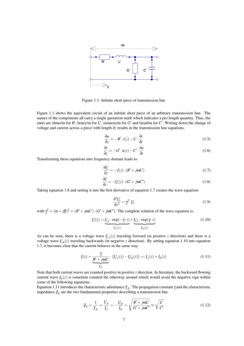
Figure 1.1: Infinite short piece of transmission line
Figure 1.1 shows the equivalent circuit of an infinite short piece of an arbitrary transmission line. Thenames of the components all carry a single quotation mark which indicates a per-length quantity. Thus, theunits are ohms/m for R′, henry/m for L′, siemens/m for G′ and farad/m for C′. Writing down the change ofvoltage and current across a piece with length ∂z results in the transmission line equations.
∂u∂z
=−R′ · i(z)−L′ · ∂i∂t
(1.5)
∂i∂z
=−G′ ·u(z)−C′ · ∂u∂t
(1.6)
Transforming these equations into frequency domain leads to:
∂U∂z
=−I(z) ·(R′+ jωL′) (1.7)
∂I∂z
=−U(z) ·(G′+ jωC′) (1.8)
Taking equation 1.8 and setting it into the first derivative of equation 1.7 creates the wave equation:
∂2U∂z2 = γ
2 ·U (1.9)
with γ2 = (α+ jβ)2 = (R′+ jωL′) ·(G′+ jωC′). The complete solution of the wave equation is:
U(z) = U1 · exp(−γ ·z)︸ ︷︷ ︸U f (z)
+U2 · exp(γ ·z)︸ ︷︷ ︸Ub(z)
(1.10)
As can be seen, there is a voltage wave U f (z) traveling forward (in positive z direction) and there is avoltage wave Ub(z) traveling backwards (in negative z direction). By setting equation 1.10 into equation1.7, it becomes clear that the current behaves in the same way:
I(z) =γ
R′+ jωL′︸ ︷︷ ︸Y L
·(U f (z)−Ub(z)
)=: I f (z)+ Ib(z) (1.11)
Note that both current waves are counted positive in positive z direction. In literature, the backward flowingcurrent wave Ib(z) is sometime counted the otherway around which would avoid the negative sign withinsome of the following equations.Equation 1.11 introduces the characteristic admittance Y L. The propagation constant γ and the characteristicimpedance ZL are the two fundamental properties describing a transmission line.
ZL =1
Y L=
U f
I f=−Ub
Ib=
√R′+ jωL′
G′+ jωC′≈√
L′
C′(1.12)
7
Note that ZL is a real value if the line loss (due to R′ and G′) is small. This is often the case in reality. Afurther very important quantity is the reflexion coefficient r which is defined as follows:
r =Ub
U f=− Ib
I f=
Ze−ZL
Ze +ZL(1.13)
The equation shows that a part of the voltage and current wave is reflected back if the end of a transmis-sion line is not terminated by an impedance that equals ZL. The same effect occurs in the middle of atransmission line, if its characteristic impedance changes.
U = U f +Ub I = I f + Ib
U f = 12 ·(U + I ·ZL) I f = 1
2 ·(U/ZL + I)
Ub = 12 ·(U− I ·ZL) Ib = 1
2 ·(I−U/ZL)
1.3 Computing with S-parameters
1.3.1 S-parameters in CAE programsThe most common task of a simulation program is to compute the S parameters of an arbitrary network thatconsists of many elementary components connected to each other. To perform this, one can build a largematrix containing the S parameters of all components and then use matrix operations to solve it. Howeverthis method needs heavy algorithms. A more elegant possibility was published in [2]. Each step computesonly one connection and so unites two connected components to a single S parameter block. This procedurehas to be done with every connection until there is only one block left whose S parameters therefore arethe simulation result.
Connecting port k of circuit (S) with port l of circuit (T ), the new S-parameters are
S′i j = Si j +Sk j ·T ll ·Sik
1−Skk ·T ll(1.14)
with i and j both being ports of (S). Furthermore, it is
S′m j =Sk j ·T ml
1−Skk ·T ll(1.15)
with m being a port of the circuit (T ). If two ports of the same circuit (S) are connected, the new S-parameters are
S′i j = Si j +Sk j ·Sil ·(1−Slk)+Sl j ·Sik ·(1−Skl)+Sk j ·Sll ·Sik +Sl j ·Skk ·Sil
(1−Skl) ·(1−Slk)−Skk ·Sll. (1.16)
If more than two ports are connected at a node, one have to insert one or more ideal tee components. ItsS-parameters write as follows. (
S)
=13·
−1 2 22 −1 22 2 −1
(1.17)
For optimisation reasons it may be desirable to insert a cross if at least four components are connected atone node. Its S-parameters write as follows.
(S)
=12·
−1 1 1 11 −1 1 11 1 −1 11 1 1 −1
(1.18)
8
The formulas (1.14), (1.15) and (1.16) were obtained using the “nontouching-loop” rule being an analyticalmethod for solving a flow graph. A few basic definitions have to be understood.
A “path” is a series of branches into the same direction with no node touched more than once. A pathsvalue is the product of the coefficients of the branches. A “loop” is formed when a path starts and finishesat the same node. A “first-order” loop is a path coming to closure with no node passed more than once. Itsvalue is the product of the values of all branches encountered on the route. A “second-order” loop consistsof two first-order loops not touching each other at any node. Its value is calculated as the product of thevalues of the two first-order loops. Third- and higher-order loops are three or more first-order loops nottouching each other at any node.
The nontouching-loop rule can be applied to solve any flow graph. In the following equation in symbolicform T represents the ratio of the dependent variable in question and the independent variable.
T =
P1 ·(
1−ΣL(1)1 +ΣL(1)
2 −ΣL(1)3 + . . .
)+P2 ·
(1−ΣL(2)
1 +ΣL(2)2 −ΣL(2)
3 + . . .)
+P3 ·(
1−ΣL(3)1 +ΣL(3)
2 −ΣL(3)3 + . . .
)+P4 · (1− . . .)+ . . .
1−ΣL1 +ΣL2−ΣL3 + . . .(1.19)
In eq. (1.19) ΣL1 stands for the sum of all first-order loops, ΣL2 is the sum of all second-order loops, andso on. P1, P2, P3 etc., stand for the values of all paths that can be found from the independent variable to thedependent variable. ΣL(1)
1 denotes the sum of those first-order loops which do not touch (hence the name)the path of P1 at any node, ΣL(1)
2 denotes then the sum of those second-order loops which do not touch thepath P1 at any point, ΣL(2)
1 consequently denotes the sum of those first-order loops which do not touch thepath of P2 at any point. Each path is multiplied by the factor in parentheses which involves all the loops ofall orders that the path does not touch.
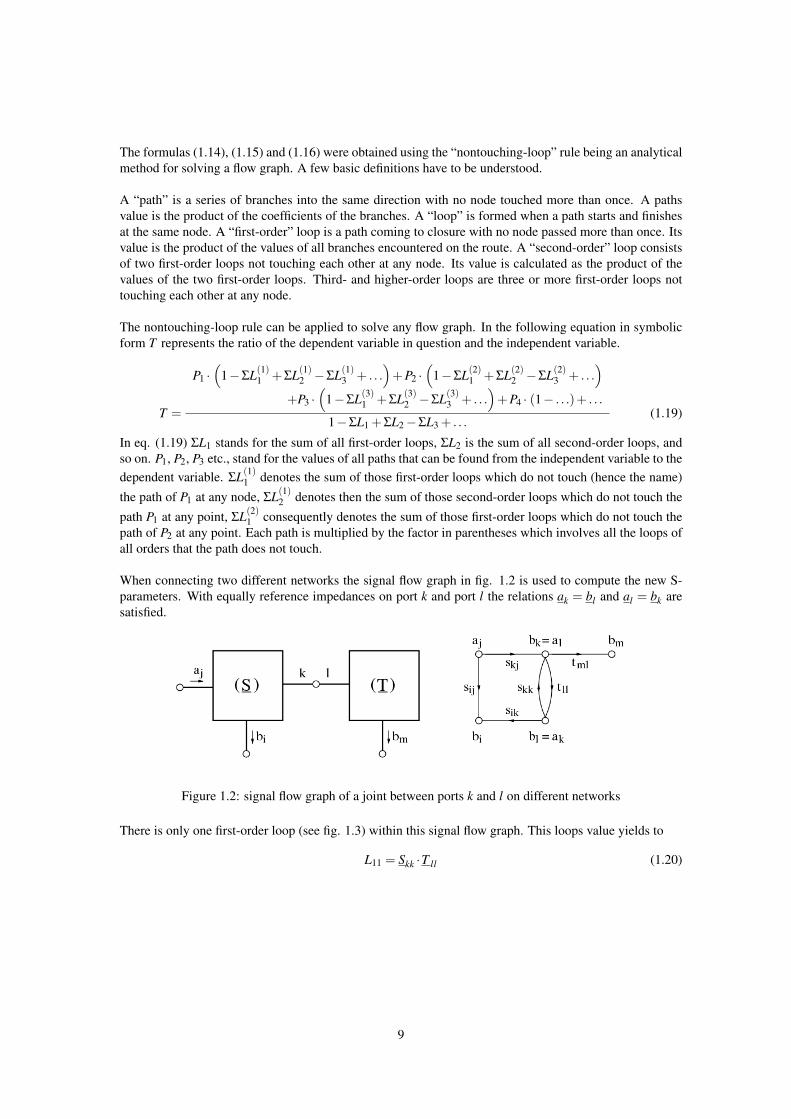
When connecting two different networks the signal flow graph in fig. 1.2 is used to compute the new S-parameters. With equally reference impedances on port k and port l the relations ak = bl and al = bk aresatisfied.
Figure 1.2: signal flow graph of a joint between ports k and l on different networks
There is only one first-order loop (see fig. 1.3) within this signal flow graph. This loops value yields to
L11 = Skk ·T ll (1.20)
9
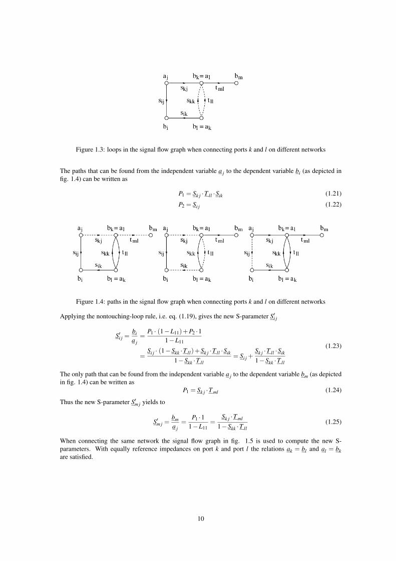
Figure 1.3: loops in the signal flow graph when connecting ports k and l on different networks
The paths that can be found from the independent variable a j to the dependent variable bi (as depicted infig. 1.4) can be written as
P1 = Sk j ·T ll ·Sik (1.21)
P2 = Si j (1.22)
Figure 1.4: paths in the signal flow graph when connecting ports k and l on different networks
Applying the nontouching-loop rule, i.e. eq. (1.19), gives the new S-parameter S′i j
S′i j =bi
a j=
P1 · (1−L11)+P2 ·11−L11
=Si j · (1−Skk ·T ll)+Sk j ·T ll ·Sik
1−Skk ·T ll= Si j +
Sk j ·T ll ·Sik
1−Skk ·T ll
(1.23)
The only path that can be found from the independent variable a j to the dependent variable bm (as depictedin fig. 1.4) can be written as
P1 = Sk j ·T ml (1.24)
Thus the new S-parameter S′m j yields to
S′m j =bm
a j=
P1 ·11−L11
=Sk j ·T ml
1−Skk ·T ll(1.25)
When connecting the same network the signal flow graph in fig. 1.5 is used to compute the new S-parameters. With equally reference impedances on port k and port l the relations ak = bl and al = bkare satisfied.
10
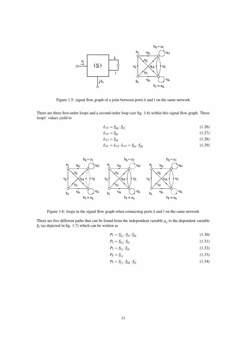
Figure 1.5: signal flow graph of a joint between ports k and l on the same network
There are three first-order loops and a second-order loop (see fig. 1.6) within this signal flow graph. Theseloops’ values yield to
L11 = Skk ·Sll (1.26)L12 = Skl (1.27)L13 = Slk (1.28)L21 = L12 ·L13 = Skl ·Slk (1.29)
Figure 1.6: loops in the signal flow graph when connecting ports k and l on the same network
There are five different paths that can be found from the independent variable a j to the dependent variablebi (as depicted in fig. 1.7) which can be written as
P1 = Sk j ·Sll ·Sik (1.30)
P2 = Sk j ·Sil (1.31)
P3 = Sl j ·Sik (1.32)
P4 = Si j (1.33)
P5 = Sl j ·Skk ·Sil (1.34)
11
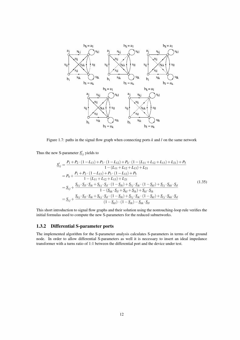
Figure 1.7: paths in the signal flow graph when connecting ports k and l on the same network
Thus the new S-parameter S′i j yields to
S′i j =P1 +P2 · (1−L13)+P3 · (1−L12)+P4 · (1− (L11 +L12 +L13)+L21)+P5
1− (L11 +L12 +L13)+L21
= P4 +P1 +P2 · (1−L13)+P3 · (1−L12)+P5
1− (L11 +L12 +L13)+L21
= Si j +Sk j ·Sll ·Sik +Sk j ·Sil · (1−Slk)+Sl j ·Sik · (1−Skl)+Sl j ·Skk ·Sil
1− (Skk ·Sll +Skl +Slk)+Skl ·Slk
= Si j +Sk j ·Sll ·Sik +Sk j ·Sil · (1−Slk)+Sl j ·Sik · (1−Skl)+Sl j ·Skk ·Sil
(1−Skl) · (1−Slk)−Skk ·Sll
(1.35)
This short introduction to signal flow graphs and their solution using the nontouching-loop rule verifies theinitial formulas used to compute the new S-parameters for the reduced subnetworks.
1.3.2 Differential S-parameter portsThe implemented algorithm for the S-parameter analysis calculates S-parameters in terms of the groundnode. In order to allow differential S-parameters as well it is necessary to insert an ideal impedancetransformer with a turns ratio of 1:1 between the differential port and the device under test.
12
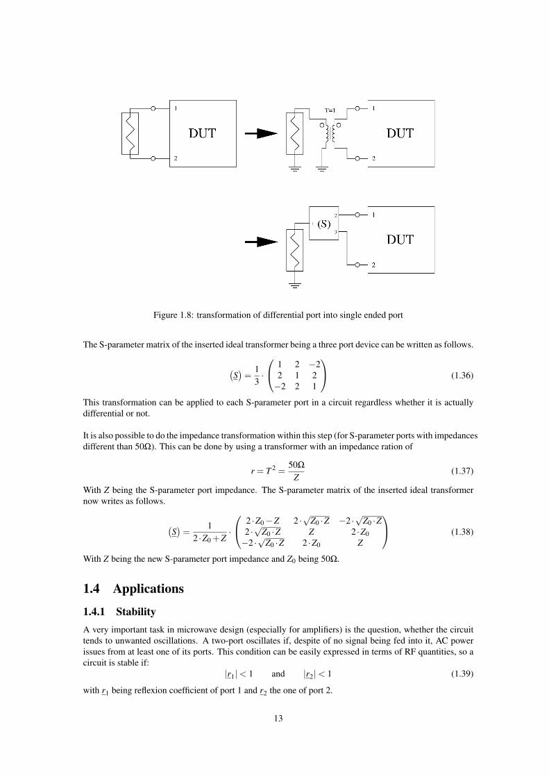
Figure 1.8: transformation of differential port into single ended port
The S-parameter matrix of the inserted ideal transformer being a three port device can be written as follows.
(S)
=13·
1 2 −22 1 2−2 2 1
(1.36)
This transformation can be applied to each S-parameter port in a circuit regardless whether it is actuallydifferential or not.
It is also possible to do the impedance transformation within this step (for S-parameter ports with impedancesdifferent than 50Ω). This can be done by using a transformer with an impedance ration of
r = T 2 =50Ω
Z(1.37)
With Z being the S-parameter port impedance. The S-parameter matrix of the inserted ideal transformernow writes as follows.
(S)
=1
2 ·Z0 +Z·
2 ·Z0−Z 2 ·√
Z0 ·Z −2 ·√
Z0 ·Z2 ·√
Z0 ·Z Z 2 ·Z0−2 ·√
Z0 ·Z 2 ·Z0 Z
(1.38)
With Z being the new S-parameter port impedance and Z0 being 50Ω.
1.4 Applications
1.4.1 StabilityA very important task in microwave design (especially for amplifiers) is the question, whether the circuittends to unwanted oscillations. A two-port oscillates if, despite of no signal being fed into it, AC powerissues from at least one of its ports. This condition can be easily expressed in terms of RF quantities, so acircuit is stable if:
|r1|< 1 and |r2|< 1 (1.39)
with r1 being reflexion coefficient of port 1 and r2 the one of port 2.
13
A further question can be asked: What conditions must be fulfilled to have a two-port be stable for all com-binations of passive impedance terminations at port 1 and port 2? Such a circuit is called unconditionallystable. [3] is one of the best discussions dealing with this subject.
A circuit is unconditionally stable if the following two relations hold:
K =1−|S11|2−|S22|2 + |∆|2
2 · |S12 ·S21|> 1 (1.40)
|∆|= |S11 ·S22−S12 ·S21|< 1 (1.41)
with ∆ being the determinant of the S parameter matrix of the two port. K is called Rollet stability factor.Two relations must be fulfilled to have a necessary and sufficient criterion.
A more practical criterion (necessary and sufficient) for unconditional stability is obtained with the µ-factor:
µ =1−|S11|2
|S22−S∗11 ·∆|+ |S12 ·S21|> 1 (1.42)
Because of symmetry reasons, a second stability factor must exist that also gives a necessary and sufficientcriterion for unconditional stability:
µ′ =1−|S22|2
|S11−S∗22 ·∆|+ |S12 ·S21|> 1 (1.43)
For conditional stable two-ports it is interesting which which load and which source impedance may causeinstability. This can be seen using stability circles [4]. A disadvantage of this method is that the radius ofthe below-mentioned circles can become infinity. (A circle with infinite radius is a line.)
Within the reflexion coefficient plane of the load (rL-plane), the stability circle is:
rcenter =S∗22−S11 ·∆∗
|S22|2−|∆|2(1.44)
Radius =|S12| · |S21||S22|2−|∆|2
(1.45)
If the center of the rL-plane lies within this circle and |S11| ≤ 1 then the circuit is stable for all reflexioncoefficients inside the circle. If the center of the rL-plane lies outside the circle and |S11| ≤ 1 then the circuitis stable for all reflexion coefficients outside the circle.
Very similar is the situation for reflexion coefficients in the source plane (rS-plane). The stability circle is:
rcenter =S∗11−S22 ·∆∗
|S11|2−|∆|2(1.46)
Radius =|S12| · |S21||S11|2−|∆|2
(1.47)
If the center of the rS-plane lies within this circle and |S22| ≤ 1 then the circuit is stable for all reflexioncoefficients inside the circle. If the center of the rS-plane lies outside the circle and |S22| ≤ 1 then the circuitis stable for all reflexion coefficients outside the circle.
14
1.4.2 GainMaximum available and stable power gain (only for unconditional stable 2-ports) [4]:
Gmax =∣∣∣∣S21
S12
∣∣∣∣ · (K−√
K2−1)
(1.48)
where K is Rollet stability factor.
The (bilateral) transmission power gain of a two-port can be split into three parts [4]:
G = GS ·G0 ·GL (1.49)
with
GS =(1−|rS|2) ·(1−|r1|2)
|1− rS ·r1|2(1.50)
G0 = |S21|2 (1.51)
GL =1−|rL|2
|1− rL ·S22|2 ·(1−|r1|2)(1.52)
where r1 is reflexion coefficient of the two-port input.
The curves of constant gain are circles in the reflexion coefficient plane. The circle for the load-mismatchedtwo-port with gain GL is
rcenter =(S∗22−S11 ·∆∗) ·GL
GL ·(|S22|2−|∆|2)+1(1.53)
Radius =
√1−GL ·(1−|S11|2−|S22|2 + |∆|2)+G2
L · |S12 ·S21|2
GL ·(|S22|2−|∆|2)+1(1.54)
The circle for the source-mismatched two-port with gain GS is
rcenter =GS ·r∗1
1−|r1|2 ·(1−GS)(1.55)
Radius =√
1−GS ·(1−|r1|2)1−|r1|2 ·(1−GS)
(1.56)
withr1 = S11 +
S12 ·S21 ·rL
1− rL ·S22(1.57)
The available power gain GA of a two-port is reached when the load is conjugately matched to the outputport. It is:
GA =|S21|2 ·(1−|rS|2)
|1−S11 ·rS|2−|S22−∆ ·rS|2(1.58)
with ∆ = S11S22−S12S21. The curves with constant gain GA are circles in the source reflexion coefficientplane (rS-plane). The center rS,c and the radius RS are:
rS,c =gA ·C∗1
1+gA ·(|S11|2−|∆|2)(1.59)
RS =
√1−2 ·K ·gA · |S12S21|+g2
A · |S12S21|2
|1+gA ·(|S11|2−|∆|2)|(1.60)
with C1 = S11−S∗22 ·∆, gA = GA/|S21|2 and K Rollet stability factor.
15
The operating power gain GP of a two-port is the power delivered to the load divided by the input power ofthe amplifier. It is:
GP =|S21|2 ·(1−|rL|2)
|1−S22 ·rL|2−|S11−∆ ·rL|2(1.61)
with ∆ = S11S22− S12S21. The curves with constant gain GP are circles in the load reflexion coefficientplane (rL-plane). The center rL,c and the radius RL are:
rL,c =gP ·C∗2
1+gP ·(|S22|2−|∆|2)(1.62)
RL =
√1−2 ·K ·gP · |S12S21|+g2
P · |S12S21|2
|1+gP ·(|S22|2−|∆|2)|(1.63)
with C2 = S22−S∗11 ·∆, gP = GP/|S21|2 and K Rollet stability factor.
1.4.3 Two-Port MatchingObtaining concurrent power matching of input and output in a bilateral circuit is not such simple, due tothe backward transmission S12. However, in linear circuits, this task can be easily solved by the followingequations:
∆ = S11 ·S22−S12 ·S21 (1.64)
B = 1+ |S11|2−|S22|2−|∆|2 (1.65)C = S11−S∗22 ·∆ (1.66)
rS =1
2 ·C·(
B−√
B2−|2 ·C|2)
(1.67)
Here rS is the reflexion coefficient that the circuit needs to see at the input port in order to reach concurrentlymatched in- and output. For the reflexion coefficient at the output rL the same equations hold by simplychanging the indices (exchange 1 by 2 and vice versa).
16
Chapter 2
Noise Waves
2.1 DefinitionIn microwave circuits described by scattering parameters, it is advantageous to regard noise as noise waves[5]. The noise characteristics of an n-port is then defined completely by one outgoing noise wave bnoise,nat each port (see 2-port example in fig. 2.1) and the correlation between these noise sources. Therefore,mathematically, you can characterize a noisy n-port by its n× n scattering matrix (S) and its n× n noisewave correlation matrix (C).
(C) =
bnoise,1 ·b∗noise,1 bnoise,1 ·b∗noise,2 . . . bnoise,1 ·b∗noise,nbnoise,2 ·b∗noise,1 bnoise,2 ·b∗noise,2 . . . bnoise,2 ·b∗noise,n
......
. . ....
bnoise,n ·b∗noise,1 bnoise,n ·b∗noise,2 . . . bnoise,n ·b∗noise,n
=
c11 c12 . . . c1nc21 c22 . . . c2n...
.... . .
...cn1 cn2 . . . cnn
(2.1)
Where x is the time average of x and x∗ is the conjugate complex of x. Noise correlation matrices arehermitian matrices because the following equations hold.
Im(cnn) = Im(|bnoise,n|2
)= 0 (2.2)
cnm = c∗mn (2.3)
Where Im(x) is the imaginary part of x and |x| is the magnitude of x.
17
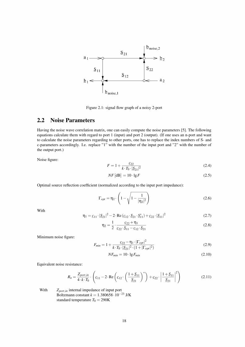
Figure 2.1: signal flow graph of a noisy 2-port
2.2 Noise ParametersHaving the noise wave correlation matrix, one can easily compute the noise parameters [5]. The followingequations calculate them with regard to port 1 (input) and port 2 (output). (If one uses an n-port and wantto calculate the noise parameters regarding to other ports, one has to replace the index numbers of S- andc-parameters accordingly. I.e. replace ”1” with the number of the input port and ”2” with the number ofthe output port.)
Noise figure:F = 1+
c22
k ·T0 · |S21|2(2.4)
NF [dB] = 10 · lgF (2.5)
Optimal source reflection coefficient (normalized according to the input port impedance):
Γopt = η2 ·
(1−
√1− 1|η2|2
)(2.6)
Withη1 = c11 · |S21|2−2 ·Re(c12 ·S21 ·S∗11)+ c22 · |S11|2 (2.7)
η2 =12· c22 +η1
c22 ·S11− c12 ·S21(2.8)
Minimum noise figure:
Fmin = 1+c22−η1 · |Γopt |2
k ·T0 · |S21|2 ·(1+ |Γopt |2)(2.9)
NFmin = 10 · lgFmin (2.10)
Equivalent noise resistance:
Rn =Zport,in
4 ·k ·T0·
(c11−2 ·Re
(c12 ·
(1+S11
S21
)∗)+ c22 ·
∣∣∣∣1+S11S21
∣∣∣∣2)
(2.11)
With Zport,in internal impedance of input portBoltzmann constant k = 1.380658 ·10−23 J/Kstandard temperature T0 = 290K
18
Calculating the noise wave correlation coefficients from the noise parameters is straightforward as well.
c11 = k ·Tmin ·(|S11|2−1)+Kx · |1−S11 ·Γopt |2 (2.12)
c22 = |S21|2 ·(k ·Tmin +Kx · |Γopt |2
)(2.13)
c12 = c∗21 =−S∗21 ·Γ∗opt ·Kx +S11
S21·c22 (2.14)
withKx =
4 ·k ·T0 ·Rn
Z0 · |1+Γopt |2(2.15)
Once having the noise parameters, one can calculate the noise figure for every source admittance YS =GS + j ·Bs, source impedance ZS = RS + j ·Xs, or source reflection coefficient rS.
F =SNRin
SNRout=
Tequi
T0+1 (2.16)
= Fmin +Gn
RS·((RS−Ropt)2 +(XS−Xopt)2) (2.17)
= Fmin +Gn
RS·∣∣ZS−Zopt
∣∣2 (2.18)
= Fmin +Rn
GS·((GS−Gopt)2 +(BS−Bopt)2) (2.19)
= Fmin +Rn
GS·∣∣Y S−Y opt
∣∣2 (2.20)
= Fmin +4 · Rn
Z0·
∣∣Γopt − rS∣∣2
(1−|rS|2) ·∣∣1+Γopt
∣∣2 (2.21)
Where SNRin and SNRout are the signal to noise ratios at the input and output, respectively, Tequi is theequivalent (input) noise temperature. Note that Gn does not equal 1/Rn.
All curves with constant noise figures are circles (in all planes, i.e. impedance, admittance and reflectioncoefficient). A circle in the reflection coefficient plane has the following parameters.
center point:
rcenter =Γopt
1+N(2.22)
radius:
R =
√N2 +N ·(1−|Γopt |2)
1+N(2.23)
withN =
Z0
4 ·Rn·(F−Fmin) · |1+Γopt |2 (2.24)
2.3 Noise Wave Correlation Matrix in CAEDue to the similar concept of S parameters and noise correlation coefficients, the CAE noise analysis canbe performed quite alike the S parameter analysis (section 1.3.1). As each step uses the S parameters tocalculate the noise correlation matrix, the noise analysis is best done step by step in parallel with the Sparameter analysis. Performing each step is as follows: We have the noise wave correlation matrices ( (C),(D) ) and the S parameter matrices ( (S), (T ) ) of two arbitrary circuits and want to know the correlationmatrix of the special circuit resulting from connecting two circuits at one port.
19
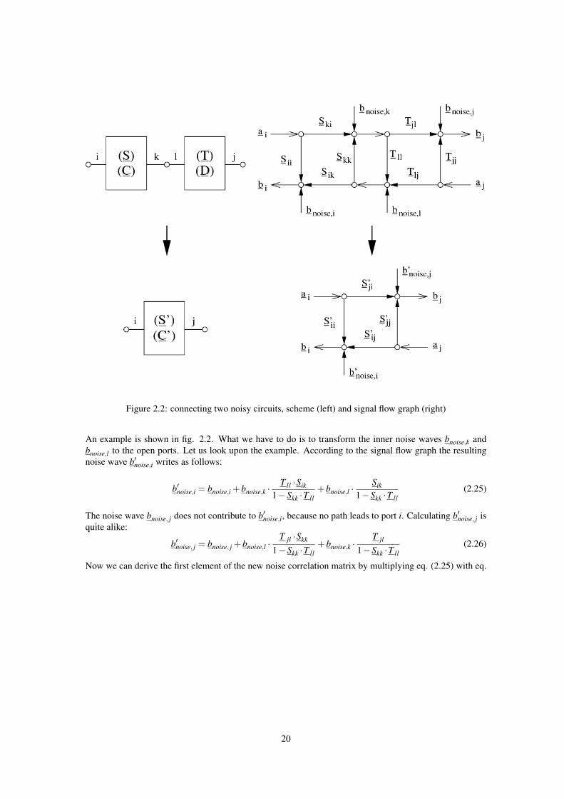
Figure 2.2: connecting two noisy circuits, scheme (left) and signal flow graph (right)
An example is shown in fig. 2.2. What we have to do is to transform the inner noise waves bnoise,k andbnoise,l to the open ports. Let us look upon the example. According to the signal flow graph the resultingnoise wave b′noise,i writes as follows:
b′noise,i = bnoise,i +bnoise,k ·T ll ·Sik
1−Skk ·T ll+bnoise,l ·
Sik
1−Skk ·T ll(2.25)
The noise wave bnoise, j does not contribute to b′noise,i, because no path leads to port i. Calculating b′noise, j isquite alike:
b′noise, j = bnoise, j +bnoise,l ·T jl ·Skk
1−Skk ·T ll+bnoise,k ·
T jl
1−Skk ·T ll(2.26)
Now we can derive the first element of the new noise correlation matrix by multiplying eq. (2.25) with eq.
20
(2.26).
c′i j = b′noise,i ·b′∗noise, j
= bnoise,i ·b∗noise, j
+bnoise,i ·b∗noise,l ·(
T jl ·Skk
1−Skk ·T ll
)∗+bnoise,i ·b∗noise,k ·
(T jl
1−Skk ·T ll
)∗+bnoise,k ·b∗noise, j ·
T ll ·Sik
1−Skk ·T ll
+bnoise,k ·b∗noise,l ·T ll ·Sik ·T ∗jl ·S
∗kk
|1−Skk ·T ll |2+bnoise,k ·b∗noise,k ·
T ll ·Sik ·T ∗jl|1−Skk ·T ll |2
+bnoise,l ·b∗noise, j ·Sik
1−Skk ·T ll
+bnoise,l ·b∗noise,l ·Sik ·T ∗jl ·S
∗kk
|1−Skk ·T ll |2+bnoise,l ·b∗noise,k ·
Sik ·T ∗jl|1−Skk ·T ll |2
(2.27)
The noise waves of different circuits are uncorrelated and therefore their time average product equals zero(e.g. bnoise,i ·b∗noise, j = 0). Thus, the final result is:
c′i j = (c′ji)∗ = (ckk ·T ll +dll ·S∗kk) ·
Sik ·T ∗jl|1−Skk ·T ll |2
+ cik ·(
T jl
1−Skk ·T ll
)∗+dl j ·
Sik
1−Skk ·T ll
(2.28)
All other cases of connecting circuits can be calculated the same way using the signal flow graph. Theresults are listed below.
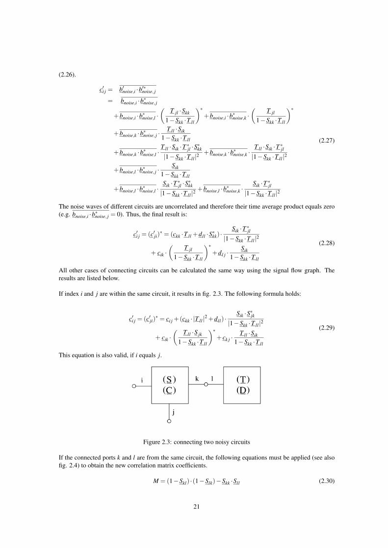
If index i and j are within the same circuit, it results in fig. 2.3. The following formula holds:
c′i j = (c′ji)∗ = ci j +(ckk · |T ll |2 +dll) ·
Sik ·S∗jk|1−Skk ·T ll |2
+ cik ·(
T ll ·S jk
1−Skk ·T ll
)∗+ ck j ·
T ll ·Sik
1−Skk ·T ll
(2.29)
This equation is also valid, if i equals j.
Figure 2.3: connecting two noisy circuits
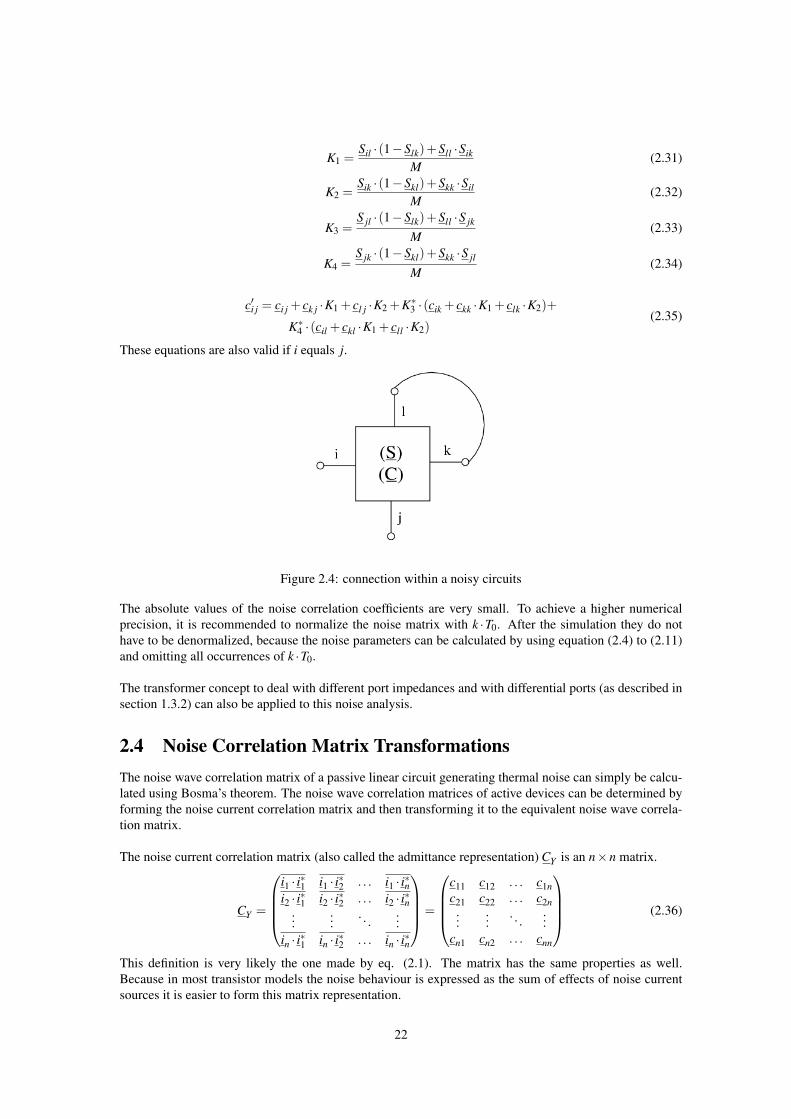
If the connected ports k and l are from the same circuit, the following equations must be applied (see alsofig. 2.4) to obtain the new correlation matrix coefficients.
M = (1−Skl) ·(1−Slk)−Skk ·Sll (2.30)
21
K1 =Sil ·(1−Slk)+Sll ·Sik
M(2.31)
K2 =Sik ·(1−Skl)+Skk ·Sil
M(2.32)
K3 =S jl ·(1−Slk)+Sll ·S jk
M(2.33)
K4 =S jk ·(1−Skl)+Skk ·S jl
M(2.34)
c′i j = ci j + ck j ·K1 + cl j ·K2 +K∗3 ·(cik + ckk ·K1 + clk ·K2)+
K∗4 ·(cil + ckl ·K1 + cll ·K2)(2.35)
These equations are also valid if i equals j.
Figure 2.4: connection within a noisy circuits
The absolute values of the noise correlation coefficients are very small. To achieve a higher numericalprecision, it is recommended to normalize the noise matrix with k ·T0. After the simulation they do nothave to be denormalized, because the noise parameters can be calculated by using equation (2.4) to (2.11)and omitting all occurrences of k ·T0.
The transformer concept to deal with different port impedances and with differential ports (as described insection 1.3.2) can also be applied to this noise analysis.
2.4 Noise Correlation Matrix TransformationsThe noise wave correlation matrix of a passive linear circuit generating thermal noise can simply be calcu-lated using Bosma’s theorem. The noise wave correlation matrices of active devices can be determined byforming the noise current correlation matrix and then transforming it to the equivalent noise wave correla-tion matrix.
The noise current correlation matrix (also called the admittance representation) CY is an n×n matrix.
CY =
i1 · i∗1 i1 · i∗2 . . . i1 · i∗ni2 · i∗1 i2 · i∗2 . . . i2 · i∗n
......
. . ....
in · i∗1 in · i∗2 . . . in · i∗n
=
c11 c12 . . . c1nc21 c22 . . . c2n...
.... . .
...cn1 cn2 . . . cnn
(2.36)
This definition is very likely the one made by eq. (2.1). The matrix has the same properties as well.Because in most transistor models the noise behaviour is expressed as the sum of effects of noise currentsources it is easier to form this matrix representation.
22
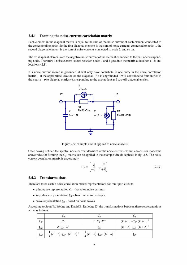
2.4.1 Forming the noise current correlation matrixEach element in the diagonal matrix is equal to the sum of the noise current of each element connected tothe corresponding node. So the first diagonal element is the sum of noise currents connected to node 1, thesecond diagonal element is the sum of noise currents connected to node 2, and so on.
The off diagonal elements are the negative noise current of the element connected to the pair of correspond-ing node. Therefore a noise current source between nodes 1 and 2 goes into the matrix at location (1,2) andlocations (2,1).
If a noise current source is grounded, it will only have contribute to one entry in the noise correlationmatrix – at the appropriate location on the diagonal. If it is ungrounded it will contribute to four entries inthe matrix – two diagonal entries (corresponding to the two nodes) and two off-diagonal entries.
Figure 2.5: example circuit applied to noise analysis
Once having defined the spectral noise current densities of the noise currents within a transistor model theabove rules for forming the CY matrix can be applied to the example circuit depicted in fig. 2.5. The noisecurrent correlation matrix is accordingly
CY =
[+i21 −i21−i21 i21 + i22
](2.37)
2.4.2 TransformationsThere are three usable noise correlation matrix representations for multiport circuits.
• admittance representation CY - based on noise currents
• impedance representation CZ - based on noise voltages
• wave representation CS - based on noise waves
According to Scott W. Wedge and David B. Rutledge [5] the transformations between these representationswrite as follows.
CY CZ CS
CY CY Y ·CZ ·Y + (E +Y ) ·CS · (E +Y )+
CZ Z ·CY ·Z+ CZ (E +Z) ·CS · (E +Z)+
CS14
(E +S) ·CY · (E +S)+14
(E−S) ·CZ · (E−S)+ CS
23
The signal as well as correlation matrices in impedance and admittance representations are assumed to benormalized in the above table. E denotes the identity matrix and the + operator indicates the transposedconjugate matrix (also called adjoint or adjugate).
Each noise correlation matrix transformation requires the appropriate signal matrix representation whichcan be obtained using the formulas given in section 15.1 on page 191.
2.5 Noise Wave Correlation Matrix of ComponentsMany components do not produce any noise. Every element of their noise correlation matrix thereforeequals exactly zero. Examples are lossless, passive components, i.e. capacitors, inductors, transformers,circulators, phase shifters. Furthermore ideal voltage and current sources (without internal resistance) aswell as gyrators also do not produce any noise.
If one wants to calculate the noise wave correlation matrix of a component, the most universal methodis to take noise voltages and noise currents and then derive the noise waves by the use of equation (1.1).However, this can be very difficult.
A passive, linear circuit produces only thermal noise and thus its noise waves can be calculated withBosma’s theorem (assuming thermodynamic equilibrium).
(C) = k ·T ·((E)− (S) ·(S)∗T
)(2.38)
with (S) being the S parameter matrix and (E) identity matrix. Of course, this theorem can also be writtenwith impedance and admittance representation of the noise correlation matrix:
CZ = 4 ·k ·T ·Re(Z) (2.39)
CY = 4 ·k ·T ·Re(Y ) (2.40)
24
Chapter 3
DC Analysis
3.1 Modified Nodal AnalysisMany different kinds of network element are encountered in network analysis. For circuit analysis it isnecessary to formulate equations for circuits containing as many different types of network elements aspossible. There are various methods for equation formulation for a circuit. These are based on three typesof equations found in circuit theory:
• equations based on Kirchhoff’s voltage law (KVL)
• equations based on Kirchhoff’s current law (KCL)
• branch constitutive equations
The equations have to be formulated (represented in a computer program) automatically in a simple, com-prehensive manner. Once formulated, the system of equations has to be solved. There are two main aspectsto be considered when choosing algorithms for this purpose: accuracy and speed. The MNA, briefly forModified Nodal Analysis, has been proved to accomplish these tasks.MNA applied to a circuit with passive elements, independent current and voltage sources and active ele-ments results in a matrix equation of the form:
[A] · [x] = [z] (3.1)
For a circuit with N nodes and M independent voltage sources:
• The A matrix
– is (N+M)×(N+M) in size, and consists only of known quantities
– the N×N part of the matrix in the upper left:
∗ has only passive elements∗ elements connected to ground appear only on the diagonal∗ elements not connected to ground are both on the diagonal and off-diagonal terms
– the rest of the A matrix (not included in the N×N upper left part) contains only 1, -1 and 0(other values are possible if there are dependent current and voltage sources)
• The x matrix
– is an (N+M)×1 vector that holds the unknown quantities (node voltages and the currentsthrough the independent voltage sources)
– the top N elements are the n node voltages
25
– the bottom M elements represent the currents through the M independent voltage sources in thecircuit
• The z matrix
– is an (N+M)×1 vector that holds only known quantities
– the top N elements are either zero or the sum and difference of independent current sources inthe circuit
– the bottom M elements represent the M independent voltage sources in the circuit
The circuit is solved by a simple matrix manipulation:
[x] = [A]−1 · [z] (3.2)
Though this may be difficult by hand, it is straightforward and so is easily done by computer.
3.1.1 Generating the MNA matricesThe following section is an algorithmic approach to the concept of the Modified Nodal Analysis. Thereare three matrices we need to generate, the A matrix, the x matrix and the z matrix. Each of these will becreated by combining several individual sub-matrices.
3.1.2 The A matrixThe A matrix will be developed as the combination of 4 smaller matrices, G, B, C, and D.
A =[
G BC D
](3.3)
The A matrix is (M+N)×(M+N) (N is the number of nodes, and M is the number of independent voltagesources) and:
• the G matrix is N×N and is determined by the interconnections between the circuit elements
• the B matrix is N×M and is determined by the connection of the voltage sources
• the C matrix is M×N and is determined by the connection of the voltage sources (B and C are closelyrelated, particularly when only independent sources are considered)
• the D matrix is M×M and is zero if only independent sources are considered
Rules for making the G matrix
The G matrix is an N×N matrix formed in two steps.
1. Each element in the diagonal matrix is equal to the sum of the conductance (one over the resistance)of each element connected to the corresponding node. So the first diagonal element is the sum of con-ductances connected to node 1, the second diagonal element is the sum of conductances connectedto node 2, and so on.
2. The off diagonal elements are the negative conductance of the element connected to the pair ofcorresponding node. Therefore a resistor between nodes 1 and 2 goes into the G matrix at location(1,2) and locations (2,1).
If an element is grounded, it will only have contribute to one entry in the G matrix – at the appropriatelocation on the diagonal. If it is ungrounded it will contribute to four entries in the matrix – two diagonalentries (corresponding to the two nodes) and two off-diagonal entries.
26
Rules for making the B matrix
The B matrix is an N×M matrix with only 0, 1 and -1 elements. Each location in the matrix correspondsto a particular voltage source (first dimension) or a node (second dimension). If the positive terminal ofthe ith voltage source is connected to node k, then the element (k,i) in the B matrix is a 1. If the negativeterminal of the ith voltage source is connected to node k, then the element (k,i) in the B matrix is a -1.Otherwise, elements of the B matrix are zero.
If a voltage source is ungrounded, it will have two elements in the B matrix (a 1 and a -1 in the samecolumn). If it is grounded it will only have one element in the matrix.
Rules for making the C matrix
The C matrix is an M×N matrix with only 0, 1 and -1 elements. Each location in the matrix corresponds toa particular node (first dimension) or voltage source (second dimension). If the positive terminal of the ithvoltage source is connected to node k, then the element (i,k) in the C matrix is a 1. If the negative terminalof the ith voltage source is connected to node k, then the element (i,k) in the C matrix is a -1. Otherwise,elements of the C matrix are zero.
In other words, the C matrix is the transpose of the B matrix. This is not the case when dependent sourcesare present.
Rules for making the D matrix
The D matrix is an M×M matrix that is composed entirely of zeros. It can be non-zero if dependent sourcesare considered.
3.1.3 The x matrixThe x matrix holds our unknown quantities and will be developed as the combination of 2 smaller matricesv and j. It is considerably easier to define than the A matrix.
x =[
vj
](3.4)
The x matrix is 1×(M+N) (N is the number of nodes, and M is the number of independent voltage sources)and:
• the v matrix is 1×N and hold the unknown voltages
• the j matrix is 1×M and holds the unknown currents through the voltage sources
Rules for making the v matrix
The v matrix is an 1×N matrix formed of the node voltages. Each element in v corresponds to the voltageat the equivalent node in the circuit (there is no entry for ground – node 0).
For a circuit with N nodes we get:
v =
v1v2...
vN
(3.5)
27
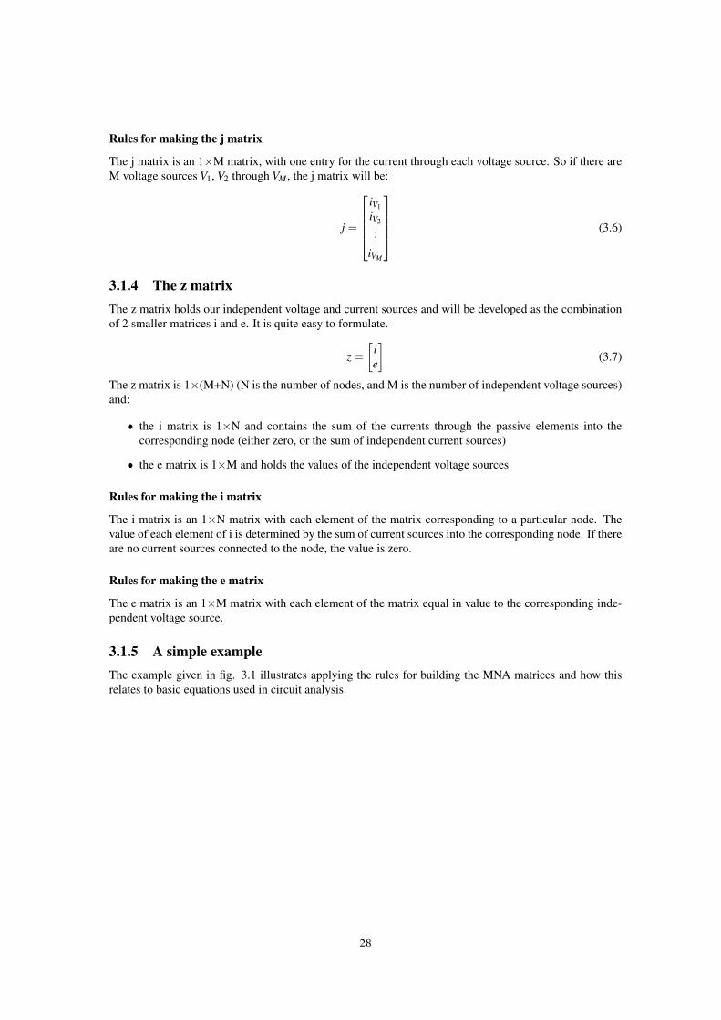
Rules for making the j matrix
The j matrix is an 1×M matrix, with one entry for the current through each voltage source. So if there areM voltage sources V1, V2 through VM , the j matrix will be:
j =
iV1
iV2...
iVM
(3.6)
3.1.4 The z matrixThe z matrix holds our independent voltage and current sources and will be developed as the combinationof 2 smaller matrices i and e. It is quite easy to formulate.
z =[
ie
](3.7)
The z matrix is 1×(M+N) (N is the number of nodes, and M is the number of independent voltage sources)and:
• the i matrix is 1×N and contains the sum of the currents through the passive elements into thecorresponding node (either zero, or the sum of independent current sources)
• the e matrix is 1×M and holds the values of the independent voltage sources
Rules for making the i matrix
The i matrix is an 1×N matrix with each element of the matrix corresponding to a particular node. Thevalue of each element of i is determined by the sum of current sources into the corresponding node. If thereare no current sources connected to the node, the value is zero.
Rules for making the e matrix
The e matrix is an 1×M matrix with each element of the matrix equal in value to the corresponding inde-pendent voltage source.
3.1.5 A simple exampleThe example given in fig. 3.1 illustrates applying the rules for building the MNA matrices and how thisrelates to basic equations used in circuit analysis.
28
Figure 3.1: example circuit applied to modified nodal analysis
Going through the MNA algorithm
The G matrix is a 2×2 matrix because there are 2 different nodes apart from ground which is the referencenode. On the diagonal you find the sum of the elements conductances connected to the nodes 1 and 2.The off-diagonal matrix entries contain the negative conductances of the elements connected between twonodes.
G =
[1
R1− 1
R1− 1
R11
R1+ 1
R2
]=[
0.2 −0.2−0.2 0.3
](3.8)
The B matrix (which is transposed to C) is a 1×2 matrix because there is one voltage source and 2 nodes.The positive terminal of the voltage source V1 is connected to node 1. That is why
B = CT =[
10
](3.9)
and the D matrix is filled with zeros only because there are no dependent (active and controlled) devices inthe example circuit.
D =[0]
(3.10)
The x matrix is a 1×3 matrix. The MNA equations deliver a solution for the unknown voltages at eachnode in a circuit except the reference node and the currents through each voltage source.
x =
v1v2iV1
(3.11)
The z matrix is according to the rules for building it a 1×3 matrix. The upper two entries are the sums ofthe currents flowing into node 1 and node 2. The lower entry is the voltage value of the voltage source V1.
z =
0I1U1
=
011
(3.12)
According to the MNA algorithm the equation system is represented by
[A] · [x] = [z] (3.13)
which is equivalent to [G BC D
]·[x]=[z]
(3.14)
29
In the example eq. (3.14) expands to: 1R1
− 1R1
1− 1
R11
R1+ 1
R20
1 0 0
·v1
v2iV1
=
0I1U1
(3.15)
The equation systems to be solved is now defined by the following matrix representation. 0.2 −0.2 1−0.2 0.3 0
1 0 0
·v1
v2iV1
=
011
(3.16)
Using matrix inversion the solution vector x writes as follows:
[x] = [A]−1 · [z] =
v1v2iV1
=
14
0.6
(3.17)
The result in eq. (3.17) denotes the current through the voltage source V1 is 0.6A, the voltage at node 1 is1V and the voltage at node 2 is 4V.
How the algorithm relates to basic equations in circuit analysis
Expanding the matrix representation in eq. (3.15) to a set of equations denotes the following equationsystem consisting of 3 of them.
I : 0 =1
R1·v1−
1R1·v2 + iV1 KCL at node 1 (3.18)
II : I1 =− 1R1·v1 +
(1
R1+
1R2
)·v2 KCL at node 2 (3.19)
III : U1 = v1 constitutive equation (3.20)
Apparently eq. I and eq. II conform to Kirchhoff’s current law at the nodes 1 and 2. The last equation isjust the constitutive equation for the voltage source V1. There are three unknowns (v1, v2 and iV1 ) and threeequations, thus the system should be solvable.
Equation III indicates the voltage at node 1 is 1V. Applying this result to eq. II and transposing it to v2 (thevoltage at node 2) gives
v2 =I1 + 1
R1·U1
1R1
+ 1R2
= 4V (3.21)
The missing current through the voltage source V1 can be computed using both the results v2 = 4V andv1 = 1V by transforming equation I.
iV1 =1
R1·v2−
1R1·v1 = 0.6A (3.22)
The small example, shown in fig. 3.1, and the excursus into artless math verifies that the MNA algorithmand classic electrical handiwork tend to produce the same results.
3.2 Extensions to the MNAAs noted in the previous sections the D matrix is zero and the B and C matrices are transposed eachother and filled with either 1, -1 or 0 provided that there are no dependent sources within the circuit.This changes when introducing active (and controlled) elements. Examples are voltage controlled voltagesources, transformers and ideal operational amplifiers. The models are depicted in section 10 and 9
30
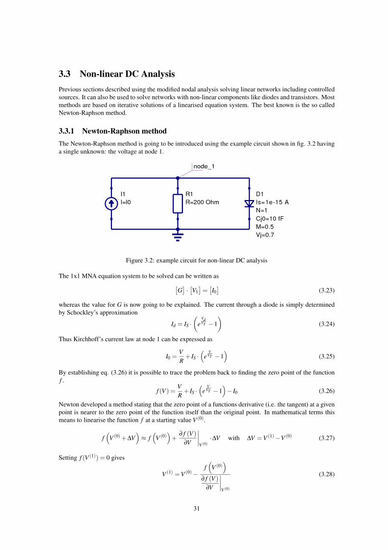
3.3 Non-linear DC AnalysisPrevious sections described using the modified nodal analysis solving linear networks including controlledsources. It can also be used to solve networks with non-linear components like diodes and transistors. Mostmethods are based on iterative solutions of a linearised equation system. The best known is the so calledNewton-Raphson method.
3.3.1 Newton-Raphson methodThe Newton-Raphson method is going to be introduced using the example circuit shown in fig. 3.2 havinga single unknown: the voltage at node 1.
Figure 3.2: example circuit for non-linear DC analysis
The 1x1 MNA equation system to be solved can be written as[G]·[V1]=[I0]
(3.23)
whereas the value for G is now going to be explained. The current through a diode is simply determinedby Schockley’s approximation
Id = IS ·(
eVdVT −1
)(3.24)
Thus Kirchhoff’s current law at node 1 can be expressed as
I0 =VR
+ IS ·(
eV
VT −1)
(3.25)
By establishing eq. (3.26) it is possible to trace the problem back to finding the zero point of the functionf .
f (V ) =VR
+ IS ·(
eV
VT −1)− I0 (3.26)
Newton developed a method stating that the zero point of a functions derivative (i.e. the tangent) at a givenpoint is nearer to the zero point of the function itself than the original point. In mathematical terms thismeans to linearise the function f at a starting value V (0).
f(
V (0) +∆V)≈ f
(V (0)
)+
∂ f (V )∂V
∣∣∣∣V (0)·∆V with ∆V = V (1)−V (0) (3.27)
Setting f (V (1)) = 0 gives
V (1) = V (0)−f(
V (0))
∂ f (V )∂V
∣∣∣∣V (0)
(3.28)
31
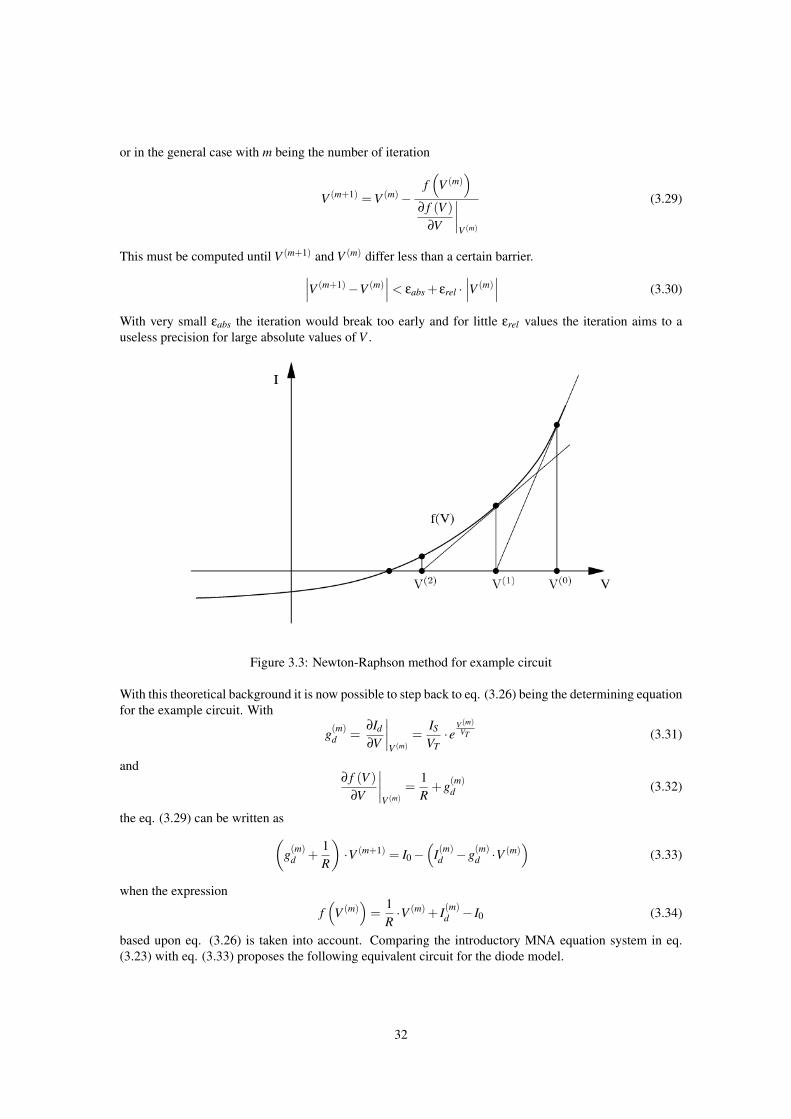
or in the general case with m being the number of iteration
V (m+1) = V (m)−f(
V (m))
∂ f (V )∂V
∣∣∣∣V (m)
(3.29)
This must be computed until V (m+1) and V (m) differ less than a certain barrier.∣∣∣V (m+1)−V (m)∣∣∣< εabs + εrel ·
∣∣∣V (m)∣∣∣ (3.30)
With very small εabs the iteration would break too early and for little εrel values the iteration aims to auseless precision for large absolute values of V .
Figure 3.3: Newton-Raphson method for example circuit
With this theoretical background it is now possible to step back to eq. (3.26) being the determining equationfor the example circuit. With
g(m)d =
∂Id
∂V
∣∣∣∣V (m)
=IS
VT·e
V (m)VT (3.31)
and∂ f (V )
∂V
∣∣∣∣V (m)
=1R
+g(m)d (3.32)
the eq. (3.29) can be written as(g(m)
d +1R
)·V (m+1) = I0−
(I(m)d −g(m)
d ·V(m))
(3.33)
when the expression
f(
V (m))
=1R·V (m) + I(m)
d − I0 (3.34)
based upon eq. (3.26) is taken into account. Comparing the introductory MNA equation system in eq.(3.23) with eq. (3.33) proposes the following equivalent circuit for the diode model.
32
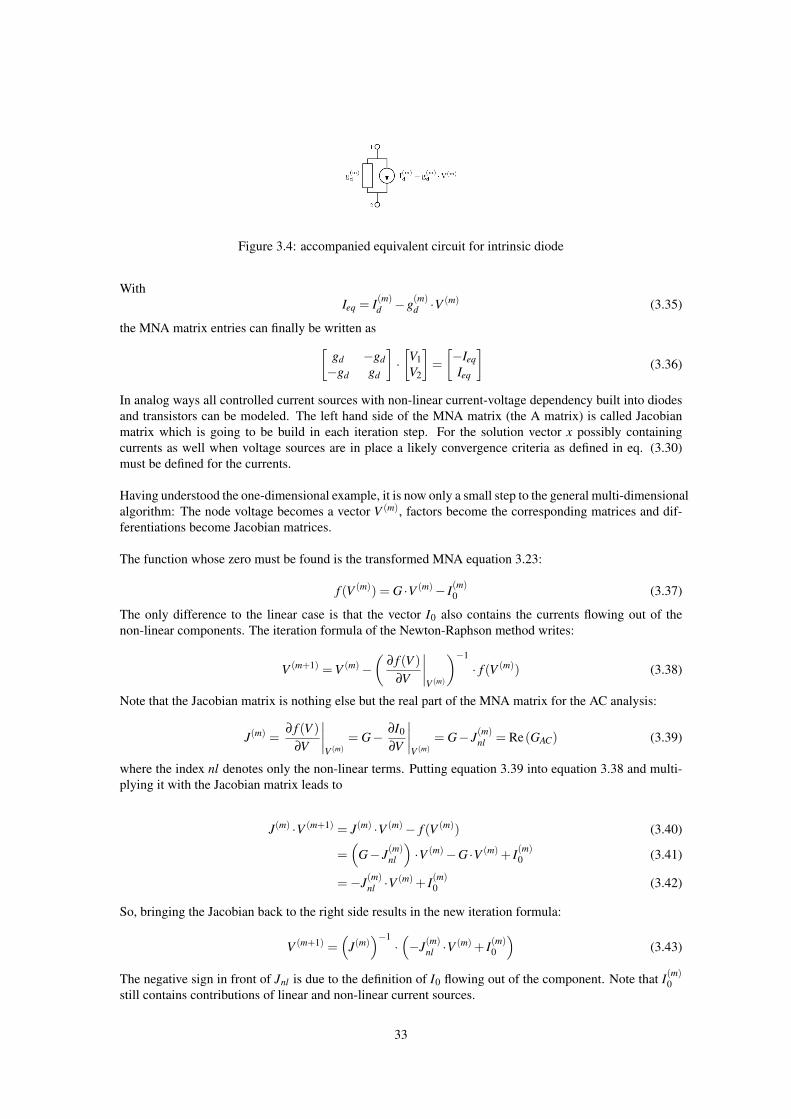
Figure 3.4: accompanied equivalent circuit for intrinsic diode
WithIeq = I(m)
d −g(m)d ·V
(m) (3.35)
the MNA matrix entries can finally be written as[gd −gd−gd gd
]·[V1V2
]=[−IeqIeq
](3.36)
In analog ways all controlled current sources with non-linear current-voltage dependency built into diodesand transistors can be modeled. The left hand side of the MNA matrix (the A matrix) is called Jacobianmatrix which is going to be build in each iteration step. For the solution vector x possibly containingcurrents as well when voltage sources are in place a likely convergence criteria as defined in eq. (3.30)must be defined for the currents.
Having understood the one-dimensional example, it is now only a small step to the general multi-dimensionalalgorithm: The node voltage becomes a vector V (m), factors become the corresponding matrices and dif-ferentiations become Jacobian matrices.
The function whose zero must be found is the transformed MNA equation 3.23:
f (V (m)) = G ·V (m)− I(m)0 (3.37)
The only difference to the linear case is that the vector I0 also contains the currents flowing out of thenon-linear components. The iteration formula of the Newton-Raphson method writes:
V (m+1) = V (m)−(
∂ f (V )∂V
∣∣∣∣V (m)
)−1
· f (V (m)) (3.38)
Note that the Jacobian matrix is nothing else but the real part of the MNA matrix for the AC analysis:
J(m) =∂ f (V )
∂V
∣∣∣∣V (m)
= G− ∂I0
∂V
∣∣∣∣V (m)
= G− J(m)nl = Re(GAC) (3.39)
where the index nl denotes only the non-linear terms. Putting equation 3.39 into equation 3.38 and multi-plying it with the Jacobian matrix leads to
J(m) ·V (m+1) = J(m) ·V (m)− f (V (m)) (3.40)
=(
G− J(m)nl
)·V (m)−G ·V (m) + I(m)
0 (3.41)
=−J(m)nl ·V
(m) + I(m)0 (3.42)
So, bringing the Jacobian back to the right side results in the new iteration formula:
V (m+1) =(
J(m))−1·(−J(m)
nl ·V(m) + I(m)
0
)(3.43)
The negative sign in front of Jnl is due to the definition of I0 flowing out of the component. Note that I(m)0
still contains contributions of linear and non-linear current sources.
33
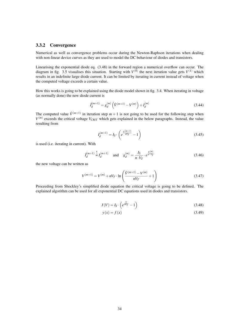
3.3.2 ConvergenceNumerical as well as convergence problems occur during the Newton-Raphson iterations when dealingwith non-linear device curves as they are used to model the DC behaviour of diodes and transistors.
Linearising the exponential diode eq. (3.48) in the forward region a numerical overflow can occur. Thediagram in fig. 3.5 visualises this situation. Starting with V (0) the next iteration value gets V (1) whichresults in an indefinite large diode current. It can be limited by iterating in current instead of voltage whenthe computed voltage exceeds a certain value.
How this works is going to be explained using the diode model shown in fig. 3.4. When iterating in voltage(as normally done) the new diode current is
I(m+1)d = g(m)
d
(V (m+1)−V (m)
)+ I(m)
d (3.44)
The computed value V (m+1) in iteration step m + 1 is not going to be used for the following step whenV (m) exceeds the critical voltage VCRIT which gets explained in the below paragraphs. Instead, the valueresulting from
I(m+1)d = IS ·
(e
V (m+1)nVT −1
)(3.45)
is used (i.e. iterating in current). With
I(m+1)d
!= I(m+1)
d and g(m)d =
IS
n ·VT·e
V (m)n·VT (3.46)
the new voltage can be written as
V (m+1) = V (m) +nVT · ln
(V (m+1)−V (m)
nVT+1
)(3.47)
Proceeding from Shockley’s simplified diode equation the critical voltage is going to be defined. Theexplained algorithm can be used for all exponential DC equations used in diodes and transistors.
I (V ) = IS ·(
eV
nVT −1)
(3.48)
y(x) = f (x) (3.49)
34
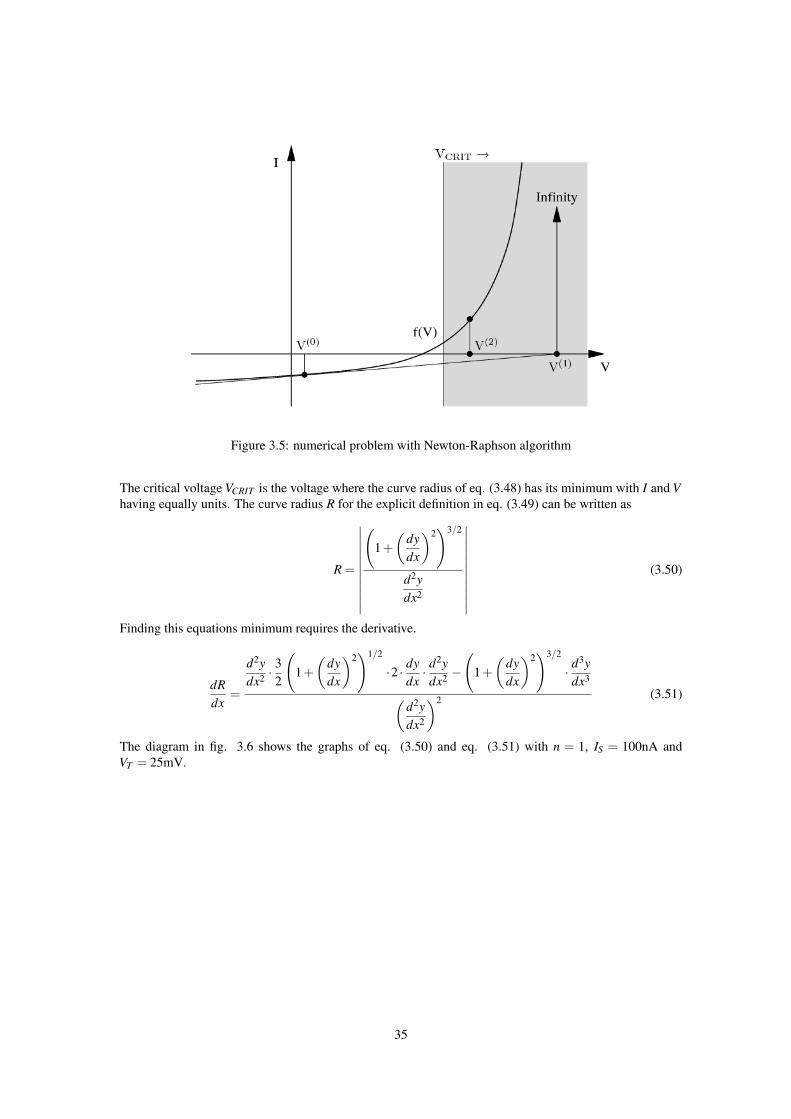
Figure 3.5: numerical problem with Newton-Raphson algorithm
The critical voltage VCRIT is the voltage where the curve radius of eq. (3.48) has its minimum with I and Vhaving equally units. The curve radius R for the explicit definition in eq. (3.49) can be written as
R =
∣∣∣∣∣∣∣∣∣∣∣
(1+(
dydx
)2)3/2
d2ydx2
∣∣∣∣∣∣∣∣∣∣∣(3.50)
Finding this equations minimum requires the derivative.
dRdx
=
d2ydx2 ·
32
(1+(
dydx
)2)1/2
·2 · dydx· d
2ydx2 −
(1+(
dydx
)2)3/2
· d3y
dx3(d2ydx2
)2 (3.51)
The diagram in fig. 3.6 shows the graphs of eq. (3.50) and eq. (3.51) with n = 1, IS = 100nA andVT = 25mV.
35
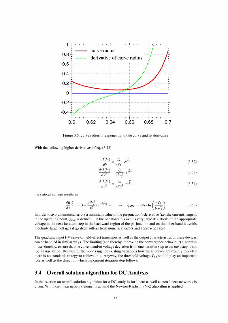
Figure 3.6: curve radius of exponential diode curve and its derivative
With the following higher derivatives of eq. (3.48)
dI (V )dV
=IS
nVT·e
VnVT (3.52)
d2I (V )dV 2 =
IS
n2V 2T·e
VnVT (3.53)
d3I (V )dV 3 =
IS
n3V 3T·e
VnVT (3.54)
the critical voltage results in
dRdx
!= 0 = 3− n2V 2
T
I2S·e−2 V
nVT −1 → VCRIT = nVT · ln(
nVT
IS√
2
)(3.55)
In order to avoid numerical errors a minimum value of the pn-junction’s derivative (i.e. the currents tangentin the operating point) gmin is defined. On the one hand this avoids very large deviations of the appropriatevoltage in the next iteration step in the backward region of the pn-junction and on the other hand it avoidsindefinite large voltages if gd itself suffers from numerical errors and approaches zero.
The quadratic input I-V curve of field-effect transistors as well as the output characteristics of these devicescan be handled in similar ways. The limiting (and thereby improving the convergence behaviour) algorithmmust somehow ensure that the current and/or voltage deviation from one iteration step to the next step is nottoo a large value. Because of the wide range of existing variations how these curves are exactly modeledthere is no standard strategy to achieve this. Anyway, the threshold voltage VT h should play an importantrole as well as the direction which the current iteration step follows.
3.4 Overall solution algorithm for DC AnalysisIn this section an overall solution algorithm for a DC analysis for linear as well as non-linear networks isgiven. With non-linear network elements at hand the Newton-Raphson (NR) algorithm is applied.
36
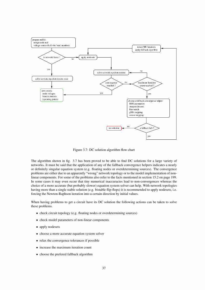
Figure 3.7: DC solution algorithm flow chart
The algorithm shown in fig. 3.7 has been proved to be able to find DC solutions for a large variety ofnetworks. It must be said that the application of any of the fallback convergence helpers indicates a nearlyor definitely singular equation system (e.g. floating nodes or overdetermining sources). The convergenceproblems are either due to an apparently “wrong” network topology or to the model implementation of non-linear components. For some of the problems also refer to the facts mentioned in section 15.2 on page 199.In some cases it may even occur that tiny numerical inaccuracies lead to non-convergences whereas thechoice of a more accurate (but probably slower) equation system solver can help. With network topologieshaving more than a single stable solution (e.g. bistable flip-flops) it is recommended to apply nodesets, i.e.forcing the Newton-Raphson iteration into a certain direction by initial values.
When having problems to get a circuit have its DC solution the following actions can be taken to solvethese problems.
• check circuit topology (e.g. floating nodes or overdetermining sources)
• check model parameters of non-linear components
• apply nodesets
• choose a more accurate equation system solver
• relax the convergence tolerances if possible
• increase the maximum iteration count
• choose the prefered fallback algorithm
37

The presented concepts are common to most circuit simulators each having to face the mentioned aspects.And probably facing it in a different manner with more or less big differences in their implementationdetails especially regarding the (fallback) convergence helpers. None of the algorithms based on Newton-Raphson ensures global convergence, thus very few documents have been published either for the complex-ity of the topic or for uncertainties in the detailed implementation each carrying the attribute “can help” or“may help”.
So for now the application of a circuit simulator to find the DC solution of a given network sometimeskeeps being a task for people knowing what they want to achieve and what they can roughly expect.
38
Chapter 4
AC Analysis
The AC analysis is a small signal analysis in the frequency domain. Basically this type of simulation usesthe same algorithms as the DC analysis (section 3.1 on page 25). The AC analysis is a linear modifiednodal analysis. Thus no iterative process is necessary. With the Y-matrix of the components, i.e. now acomplex matrix, and the appropriate extensions it is necessary to solve the equation system (4.1) similar tothe (linear) DC analysis.
[A] · [x] = [z] with A =[Y BC D
](4.1)
Non-linear components have to be linearized at the DC bias point. That is, before an AC simulation withnon-linear components can be performed, a DC simulation must be completed successfully. Then, theMNA stamp of the non-linear components equals their entries of the Jacobian matrix, which was alreadycomputed during the DC simulation. In addition to this real-valued elements, a further stamp has to beapplied: The Jacobian matrix of the non-linear charges multiplied by jω (see also section 10.7).
39
Chapter 5
AC Noise Analysis
5.1 DefinitionsFirst some definition must be done:
Reciprocal Networks:Two networks A and B are reciprocal to each other if their transimpedances have the following relation:
Zmn,A = Znm,B (5.1)
That means: Drive the current I into node n of circuit A and at node m the voltage I ·Zmn,A appears. Incircuit B it is just the way around.
Adjoint Networks:Network A and network B are adjoint to each other if the following equation holds for their MNA matrices:
[A]T = [B] (5.2)
5.2 The AlgorithmTo calculate the small signal noise of a circuit, the AC noise analysis has to be applied [6]. This techniqueuses the principle of the AC analysis described in chapter 4 on page 39. In addition to the MNA matrix Aone needs the noise current correlation matrix CY of the circuit, that contains the equivalent noise currentsources for every node on its main diagonal and their correlation on the other positions.
The basic concept of the AC noise analysis is as follows: The noise voltage at node i should be calculated,so the voltage arising due to the noise source at node j is calculated first. This has to be done for everyn nodes and after that adding all the noise voltages (by paying attention to their correlation) leads to theoverall voltage. But that would mean to solve the MNA equation n times. Fortunately there is a more easyway. One can perform the above-mentioned n steps in one single step, if the reciprocal MNA matrix isused. This matrix equals the MNA matrix itself, if the network is reciprocal. A network that only containsresistors, capacitors, inductors, gyrators and transformers is reciprocal.
The question that needs to be answered now is: How to get the reciprocal MNA matrix for an arbitrarynetwork? This is equivalent to the question: How to get the MNA matrix of the adjoint network. Theanswer is quite simple: Just transpose the MNA matrix!
40
For any network, calculating the noise voltage at node i is done by the following three steps:
1. Solving MNA equation: [A]T · [x] = [A]T ·[
vj
]=
0...0−10...0
← i-th row (5.3)
2. Creating noise correlation matrix: (CY ) (5.4)
3. Calculating noise voltage: vnoise,i =√
[v]T · (CY ) · [v]∗ (5.5)
If the correlation between several noise voltages is also wanted, the procedure is straight forward: Performstep 1 for every desired node, put the results into a matrix and replace the vector [v] in step 3 by thismatrix. This results in the complete correlation matrix. Indeed, the above-mentioned algorithm is only aspecialisation of transforming the noise correlation matrices (see section 2.4.2).
If the normal AC analysis has already be done with LU decomposition, then the most time consuming workof step 1 has already be done.
instead of Y = L ·U we have Y T = UT ·LT (5.6)
I.e. UT becomes the new L matrix and LT becomes the new U matrix, and the matrix equation do not needto be solved again, because only the right-hand side was changed. So altogether this is a quickly done task.(Note that in step 3, only the subvector [v] of vector [x] is used. See section 3.1.3 for details on this.)
If the noise voltage at another node needs to be known, only the right-hand side of step 1 changes. That is,a new LU decomposition is not needed.
Reusing the LU decomposed MNA matrix of the usual AC analysis is possible if there has been no pivotingnecessary during the decomposition.
When using either Crout’s or Doolittle’s definition of the LU decomposition during the AC analysis thedecomposition representation changes during the AC noise analysis as the matrix A gets transposed. Thismeans:
A = L ·U with L =
l11 0 . . . 0
l21 l22. . .
......
. . . 0ln1 . . . . . . lnn
and U =
1 u12 . . . u1n
0 1...
.... . . . . .
...0 . . . 0 1
(5.7)
becomes
AT = UT ·LT with L =
1 0 . . . 0
l21 1. . .
......
. . . 0ln1 . . . . . . 1
and U =
u11 u12 . . . u1n
0 u22...
.... . . . . .
...0 . . . 0 unn
(5.8)
Thus the forward substitution (as described in section 15.2.4) and the backward substitution (as describedin section 15.2.4) must be slightly modified.
yi = zi−i−1
∑k=1
yk · lik i = 1, . . . ,n (5.9)
41
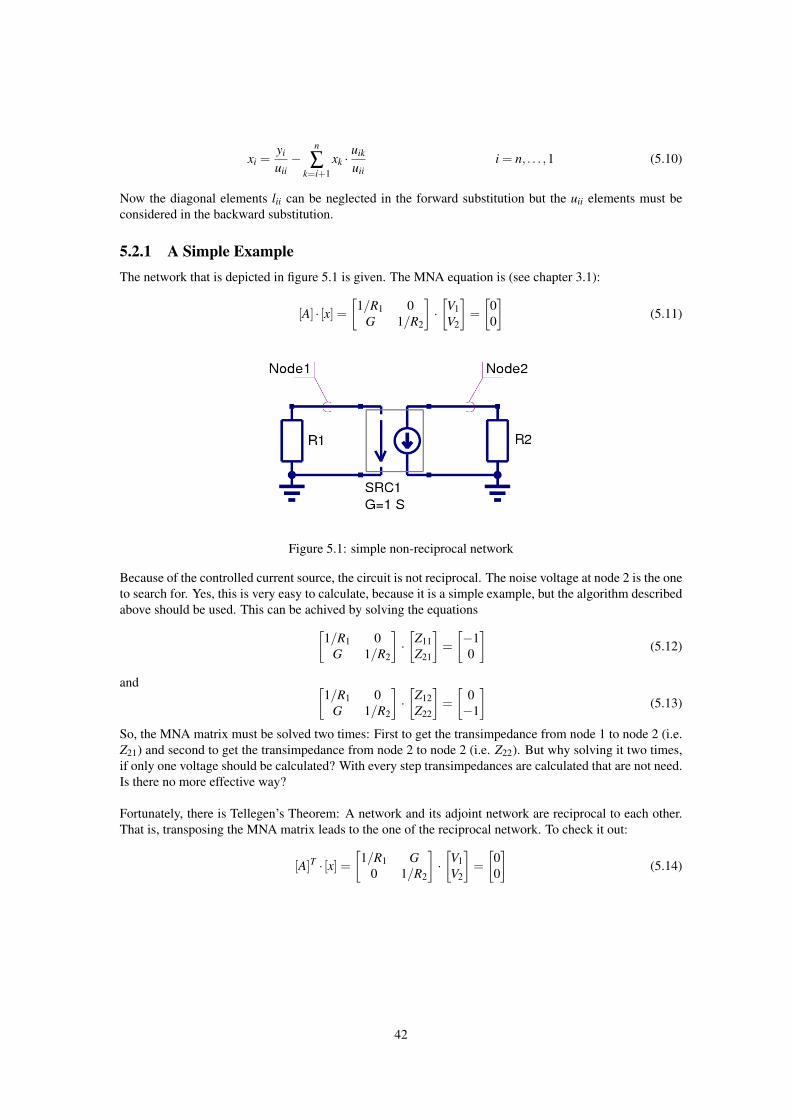
xi =yi
uii−
n
∑k=i+1
xk ·uik
uiii = n, . . . ,1 (5.10)
Now the diagonal elements lii can be neglected in the forward substitution but the uii elements must beconsidered in the backward substitution.
5.2.1 A Simple ExampleThe network that is depicted in figure 5.1 is given. The MNA equation is (see chapter 3.1):
[A] · [x] =[
1/R1 0G 1/R2
]·[V1V2
]=[
00
](5.11)
Figure 5.1: simple non-reciprocal network
Because of the controlled current source, the circuit is not reciprocal. The noise voltage at node 2 is the oneto search for. Yes, this is very easy to calculate, because it is a simple example, but the algorithm describedabove should be used. This can be achived by solving the equations[
1/R1 0G 1/R2
]·[
Z11Z21
]=[−10
](5.12)
and [1/R1 0
G 1/R2
]·[
Z12Z22
]=[
0−1
](5.13)
So, the MNA matrix must be solved two times: First to get the transimpedance from node 1 to node 2 (i.e.Z21) and second to get the transimpedance from node 2 to node 2 (i.e. Z22). But why solving it two times,if only one voltage should be calculated? With every step transimpedances are calculated that are not need.Is there no more effective way?
Fortunately, there is Tellegen’s Theorem: A network and its adjoint network are reciprocal to each other.That is, transposing the MNA matrix leads to the one of the reciprocal network. To check it out:
[A]T · [x] =[
1/R1 G0 1/R2
]·[V1V2
]=[
00
](5.14)
42
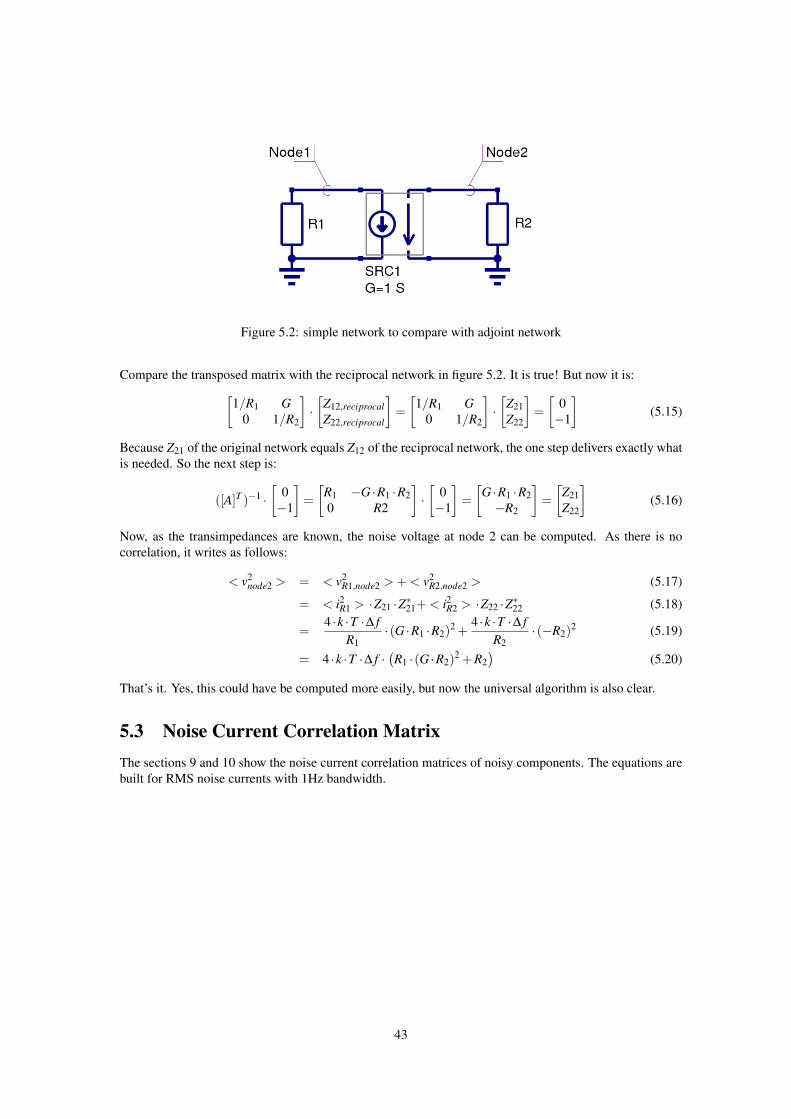
Figure 5.2: simple network to compare with adjoint network
Compare the transposed matrix with the reciprocal network in figure 5.2. It is true! But now it is:[1/R1 G
0 1/R2
]·[
Z12,reciprocalZ22,reciprocal
]=[
1/R1 G0 1/R2
]·[
Z21Z22
]=[
0−1
](5.15)
Because Z21 of the original network equals Z12 of the reciprocal network, the one step delivers exactly whatis needed. So the next step is:
([A]T )−1 ·[
0−1
]=[
R1 −G ·R1 ·R20 R2
]·[
0−1
]=[
G ·R1 ·R2−R2
]=[
Z21Z22
](5.16)
Now, as the transimpedances are known, the noise voltage at node 2 can be computed. As there is nocorrelation, it writes as follows:
< v2node2 > = < v2
R1,node2 > + < v2R2,node2 > (5.17)
= < i2R1 > ·Z21 ·Z∗21+ < i2R2 > ·Z22 ·Z∗22 (5.18)
=4 ·k ·T ·∆ f
R1·(G ·R1 ·R2)2 +
4 ·k ·T ·∆ fR2
·(−R2)2 (5.19)
= 4 ·k ·T ·∆ f ·(R1 ·(G ·R2)2 +R2
)(5.20)
That’s it. Yes, this could have be computed more easily, but now the universal algorithm is also clear.
5.3 Noise Current Correlation MatrixThe sections 9 and 10 show the noise current correlation matrices of noisy components. The equations arebuilt for RMS noise currents with 1Hz bandwidth.
43
Chapter 6
Transient Analysis
The transient simulation is the calculation of a networks response on arbitrary excitations. The results arenetwork quantities (branch currents and node voltages) as a function of time. Substantial for the transientanalysis is the consideration of energy storing components, i.e. inductors and capacitors.
The relations between current and voltage of ideal capacitors and inductors are given by
VC(t) =1C
ZIC(t) ·dt and IL(t) =
1L
ZVL(t) ·dt (6.1)
or in terms of differential equations
IC(t) = C · dVC
dtand VL(t) = L · dIL
dt(6.2)
To calculate these quantities in a computer program numerical integration methods are required. With thecurrent-voltage relations of these components at hand it is possible to apply the modified nodal analysisalgorithm in order to calculate the networks response. This means the transient analysis attempts to find anapproximation to the analytical solution at discrete time points using numeric integration.
6.1 Integration methodsThe following differential equation is going to be solved.
dxdt
= x(t) = f (x, t) (6.3)
This differential equation is transformed into an algorithm-dependent finite difference equation by quan-tizing and replacing
x(t) = limh→0
x(t +h)− x(t)h
(6.4)
by the following equation.
xn =xn+1− xn
hn (6.5)
There are several linear single- and multi-step numerical integration methods available, each having ad-vantages and disadvantages concerning aspects of stability and accuracy. Integration methods can also beclassified into implicit and explicit methods. Explicit methods are inexpensive per step but limited in stabil-ity and therefore not used in the field of circuit simulation to obtain a correct and stable solution. Implicitmethods are more expensive per step, have better stability and therefore suitable for circuit simulation.
44
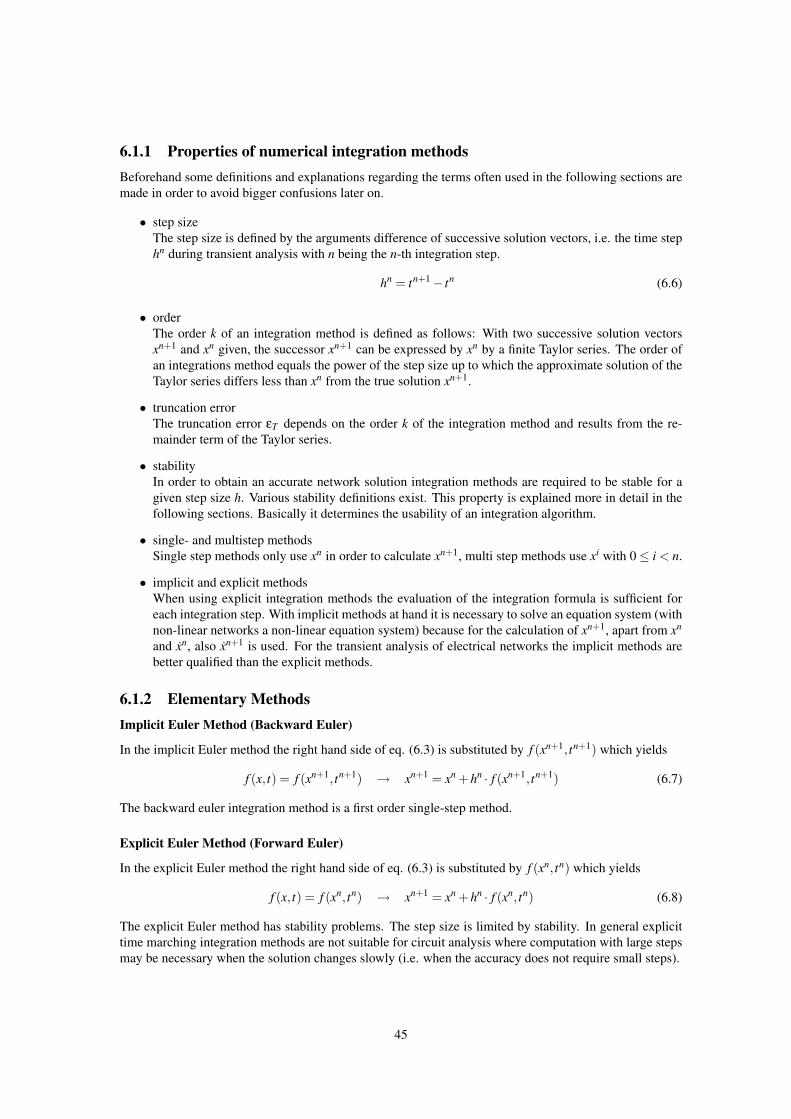
6.1.1 Properties of numerical integration methodsBeforehand some definitions and explanations regarding the terms often used in the following sections aremade in order to avoid bigger confusions later on.
• step sizeThe step size is defined by the arguments difference of successive solution vectors, i.e. the time stephn during transient analysis with n being the n-th integration step.
hn = tn+1− tn (6.6)
• orderThe order k of an integration method is defined as follows: With two successive solution vectorsxn+1 and xn given, the successor xn+1 can be expressed by xn by a finite Taylor series. The order ofan integrations method equals the power of the step size up to which the approximate solution of theTaylor series differs less than xn from the true solution xn+1.
• truncation errorThe truncation error εT depends on the order k of the integration method and results from the re-mainder term of the Taylor series.
• stabilityIn order to obtain an accurate network solution integration methods are required to be stable for agiven step size h. Various stability definitions exist. This property is explained more in detail in thefollowing sections. Basically it determines the usability of an integration algorithm.
• single- and multistep methodsSingle step methods only use xn in order to calculate xn+1, multi step methods use xi with 0≤ i < n.
• implicit and explicit methodsWhen using explicit integration methods the evaluation of the integration formula is sufficient foreach integration step. With implicit methods at hand it is necessary to solve an equation system (withnon-linear networks a non-linear equation system) because for the calculation of xn+1, apart from xn
and xn, also xn+1 is used. For the transient analysis of electrical networks the implicit methods arebetter qualified than the explicit methods.
6.1.2 Elementary MethodsImplicit Euler Method (Backward Euler)
In the implicit Euler method the right hand side of eq. (6.3) is substituted by f (xn+1, tn+1) which yields
f (x, t) = f (xn+1, tn+1) → xn+1 = xn +hn · f (xn+1, tn+1) (6.7)
The backward euler integration method is a first order single-step method.
Explicit Euler Method (Forward Euler)
In the explicit Euler method the right hand side of eq. (6.3) is substituted by f (xn, tn) which yields
f (x, t) = f (xn, tn) → xn+1 = xn +hn · f (xn, tn) (6.8)
The explicit Euler method has stability problems. The step size is limited by stability. In general explicittime marching integration methods are not suitable for circuit analysis where computation with large stepsmay be necessary when the solution changes slowly (i.e. when the accuracy does not require small steps).
45
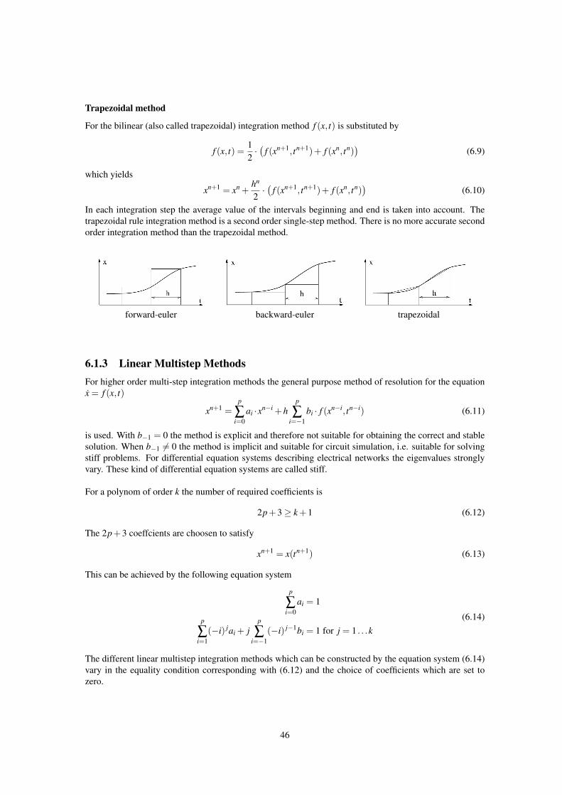
Trapezoidal method
For the bilinear (also called trapezoidal) integration method f (x, t) is substituted by
f (x, t) =12·(
f (xn+1, tn+1)+ f (xn, tn))
(6.9)
which yields
xn+1 = xn +hn
2·(
f (xn+1, tn+1)+ f (xn, tn))
(6.10)
In each integration step the average value of the intervals beginning and end is taken into account. Thetrapezoidal rule integration method is a second order single-step method. There is no more accurate secondorder integration method than the trapezoidal method.
forward-euler backward-euler trapezoidal
6.1.3 Linear Multistep MethodsFor higher order multi-step integration methods the general purpose method of resolution for the equationx = f (x, t)
xn+1 =p
∑i=0
ai ·xn−i +hp
∑i=−1
bi · f (xn−i, tn−i) (6.11)
is used. With b−1 = 0 the method is explicit and therefore not suitable for obtaining the correct and stablesolution. When b−1 6= 0 the method is implicit and suitable for circuit simulation, i.e. suitable for solvingstiff problems. For differential equation systems describing electrical networks the eigenvalues stronglyvary. These kind of differential equation systems are called stiff.
For a polynom of order k the number of required coefficients is
2p+3≥ k +1 (6.12)
The 2p+3 coeffcients are choosen to satisfy
xn+1 = x(tn+1) (6.13)
This can be achieved by the following equation system
p
∑i=0
ai = 1
p
∑i=1
(−i) jai + jp
∑i=−1
(−i) j−1bi = 1 for j = 1 . . .k(6.14)
The different linear multistep integration methods which can be constructed by the equation system (6.14)vary in the equality condition corresponding with (6.12) and the choice of coefficients which are set tozero.
46
Gear
The Gear [7] formulae (also called BDF - backward differentiation formulae) have great importance withinthe multi-step integration methods used in transient analysis programs. The conditions
p = k−1 and b0 = b1 = . . . = bk−1 = 0 (6.15)
due to the following equation system0 1 1 1 11 0 −1 −2 −32 0 1 4 93 0 −1 −8 −274 0 1 16 81
·
b−1a0a1a2a3
=
11111
(6.16)
for the Gear formulae of order 4. Order k = 1 yields the implicit Euler method. The example given in theequation system (6.16) results in the following integration formula.
xn+1 = a0 ·xn +a1 ·xn−1 +a2 ·xn−2 +a3 ·xn−3 +h ·b−1 · f (xn+1, tn+1)
=4825·xn− 36
25·xn−1 +
1625·xn−2− 3
25·xn−3 +h · 12
25· f (xn+1, tn+1)
(6.17)
There is no more stable second order integration method than the Gear’s method of second order. Onlyimplicit Gear methods with order k ≤ 6 are zero stable.
Adams-Bashford
The Adams-Bashford algorithm is an explicit multi-step integration method whence
p = k−1 and a1 = a2 = . . . = ak−1 = 0 and b−1 = 0 (6.18)
is set to satisfy the equation system (6.14). The equation system of the Adams-Bashford coefficients oforder 4 is as follows.
1 0 0 0 00 1 1 1 10 0 −2 −4 −60 0 3 12 270 0 −4 −32 −108
·
a0b0b1b2b3
=
11111
(6.19)
This equation system results in the following integration formula.
xn+1 = a0 ·xn +h ·b0 · f n +h ·b1 · f n−1 +h ·b2 · f n−2 +h ·b3 · f n−3
= xn +h · 5524· f n−h · 59
24· f n−1 +h · 37
24· f n−2−h · 9
24· f n−3
(6.20)
The Adams-Bashford formula of order 1 yields the (explicit) forward Euler integration method.
Adams-Moulton
The Adams-Moulton algorithm is an implicit multi-step integration method whence
p = k−2 and a1 = a2 = . . . = ak−2 = 0 (6.21)
is set to satisfy the equation system (6.14). The equation system of the Adams-Moulton coefficients oforder 4 is as follows.
1 0 0 0 00 1 1 1 10 2 0 −2 −40 3 0 3 120 4 0 −4 −32
·
a0b−1b0b1b2
=
11111
(6.22)
47
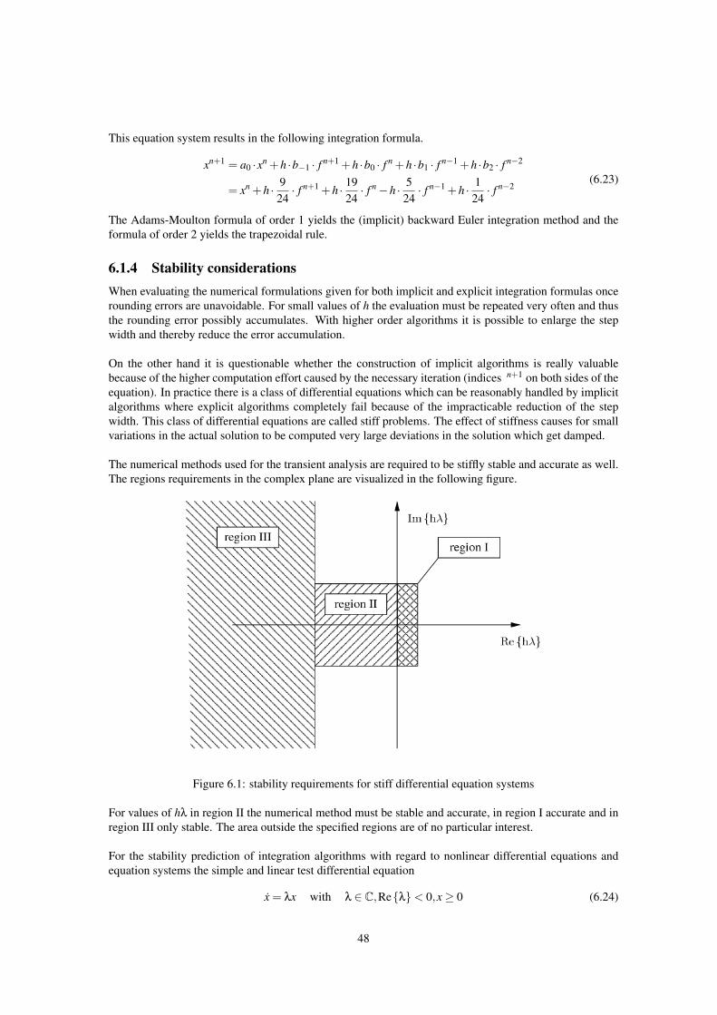
This equation system results in the following integration formula.
xn+1 = a0 ·xn +h ·b−1 · f n+1 +h ·b0 · f n +h ·b1 · f n−1 +h ·b2 · f n−2
= xn +h · 924· f n+1 +h · 19
24· f n−h · 5
24· f n−1 +h · 1
24· f n−2
(6.23)
The Adams-Moulton formula of order 1 yields the (implicit) backward Euler integration method and theformula of order 2 yields the trapezoidal rule.
6.1.4 Stability considerationsWhen evaluating the numerical formulations given for both implicit and explicit integration formulas oncerounding errors are unavoidable. For small values of h the evaluation must be repeated very often and thusthe rounding error possibly accumulates. With higher order algorithms it is possible to enlarge the stepwidth and thereby reduce the error accumulation.
On the other hand it is questionable whether the construction of implicit algorithms is really valuablebecause of the higher computation effort caused by the necessary iteration (indices n+1 on both sides of theequation). In practice there is a class of differential equations which can be reasonably handled by implicitalgorithms where explicit algorithms completely fail because of the impracticable reduction of the stepwidth. This class of differential equations are called stiff problems. The effect of stiffness causes for smallvariations in the actual solution to be computed very large deviations in the solution which get damped.
The numerical methods used for the transient analysis are required to be stiffly stable and accurate as well.The regions requirements in the complex plane are visualized in the following figure.
Figure 6.1: stability requirements for stiff differential equation systems
For values of hλ in region II the numerical method must be stable and accurate, in region I accurate and inregion III only stable. The area outside the specified regions are of no particular interest.
For the stability prediction of integration algorithms with regard to nonlinear differential equations andequation systems the simple and linear test differential equation
x = λx with λ ∈ C,Reλ< 0,x≥ 0 (6.24)
48
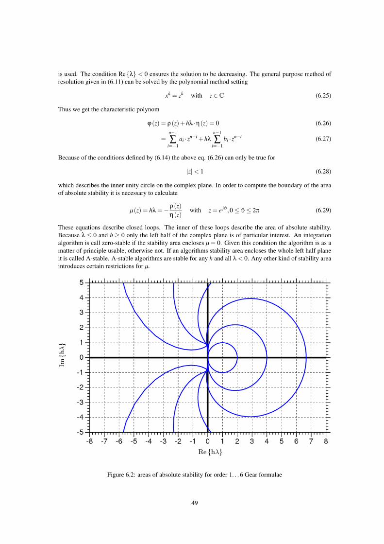
is used. The condition Reλ < 0 ensures the solution to be decreasing. The general purpose method ofresolution given in (6.11) can be solved by the polynomial method setting
xk = zk with z ∈ C (6.25)
Thus we get the characteristic polynom
ϕ(z) = ρ(z)+hλ ·η(z) = 0 (6.26)
=n−1
∑i=−1
ai ·zn−i +hλ
n−1
∑i=−1
bi ·zn−i (6.27)
Because of the conditions defined by (6.14) the above eq. (6.26) can only be true for
|z|< 1 (6.28)
which describes the inner unity circle on the complex plane. In order to compute the boundary of the areaof absolute stability it is necessary to calculate
µ(z) = hλ =−ρ(z)η(z)
with z = e jϑ,0≤ ϑ≤ 2π (6.29)
These equations describe closed loops. The inner of these loops describe the area of absolute stability.Because λ ≤ 0 and h ≥ 0 only the left half of the complex plane is of particular interest. An integrationalgorithm is call zero-stable if the stability area encloses µ = 0. Given this condition the algorithm is as amatter of principle usable, otherwise not. If an algorithms stability area encloses the whole left half planeit is called A-stable. A-stable algorithms are stable for any h and all λ < 0. Any other kind of stability areaintroduces certain restrictions for µ.
Figure 6.2: areas of absolute stability for order 1. . . 6 Gear formulae
49
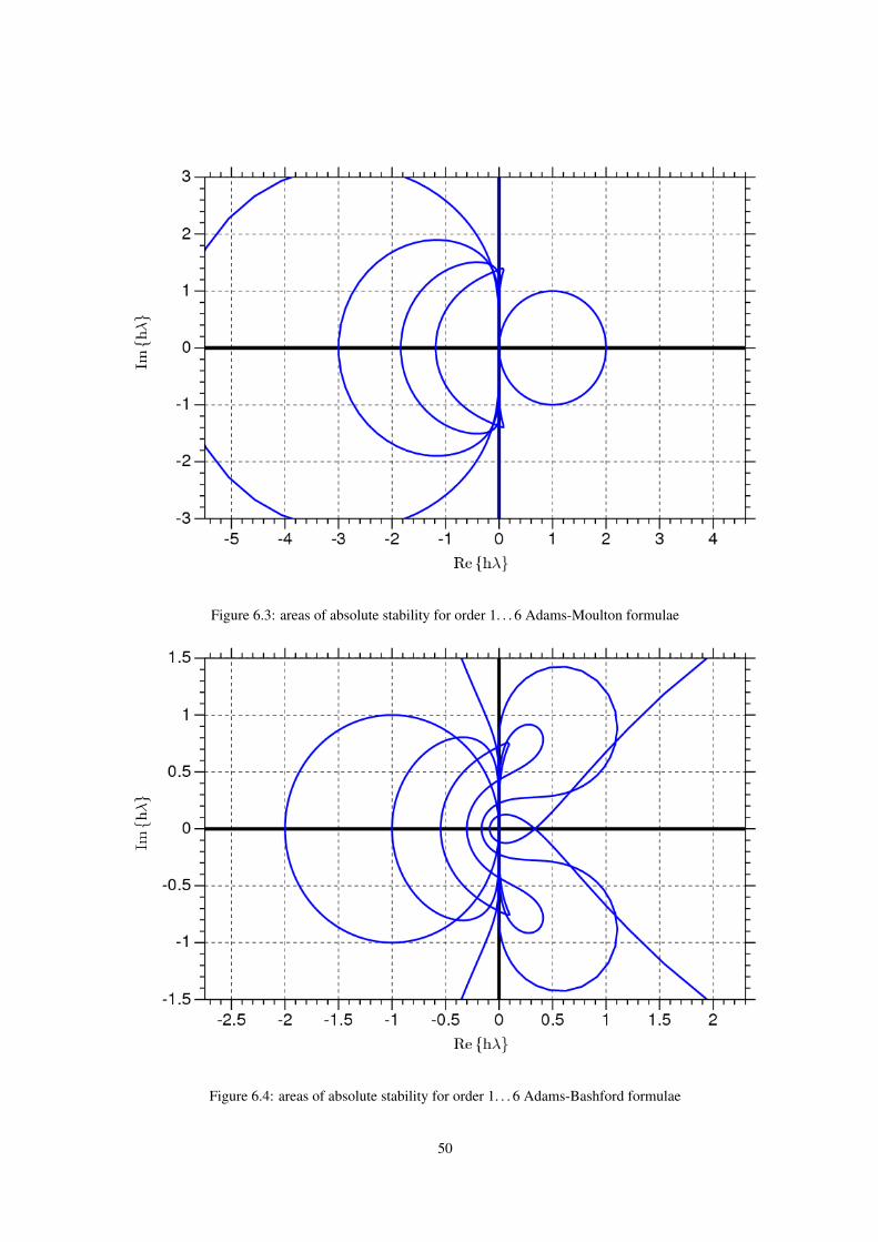
Figure 6.3: areas of absolute stability for order 1. . . 6 Adams-Moulton formulae
Figure 6.4: areas of absolute stability for order 1. . . 6 Adams-Bashford formulae
50
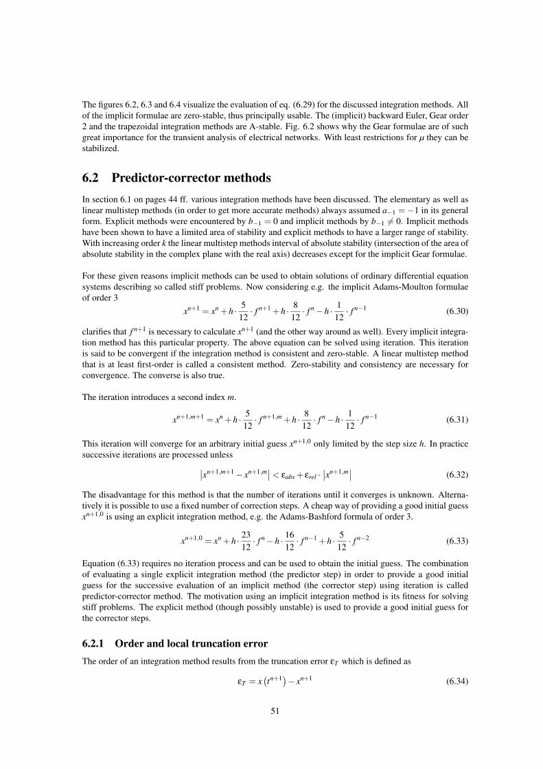
The figures 6.2, 6.3 and 6.4 visualize the evaluation of eq. (6.29) for the discussed integration methods. Allof the implicit formulae are zero-stable, thus principally usable. The (implicit) backward Euler, Gear order2 and the trapezoidal integration methods are A-stable. Fig. 6.2 shows why the Gear formulae are of suchgreat importance for the transient analysis of electrical networks. With least restrictions for µ they can bestabilized.
6.2 Predictor-corrector methodsIn section 6.1 on pages 44 ff. various integration methods have been discussed. The elementary as well aslinear multistep methods (in order to get more accurate methods) always assumed a−1 =−1 in its generalform. Explicit methods were encountered by b−1 = 0 and implicit methods by b−1 6= 0. Implicit methodshave been shown to have a limited area of stability and explicit methods to have a larger range of stability.With increasing order k the linear multistep methods interval of absolute stability (intersection of the area ofabsolute stability in the complex plane with the real axis) decreases except for the implicit Gear formulae.
For these given reasons implicit methods can be used to obtain solutions of ordinary differential equationsystems describing so called stiff problems. Now considering e.g. the implicit Adams-Moulton formulaeof order 3
xn+1 = xn +h · 512· f n+1 +h · 8
12· f n−h · 1
12· f n−1 (6.30)
clarifies that f n+1 is necessary to calculate xn+1 (and the other way around as well). Every implicit integra-tion method has this particular property. The above equation can be solved using iteration. This iterationis said to be convergent if the integration method is consistent and zero-stable. A linear multistep methodthat is at least first-order is called a consistent method. Zero-stability and consistency are necessary forconvergence. The converse is also true.
The iteration introduces a second index m.
xn+1,m+1 = xn +h · 512· f n+1,m +h · 8
12· f n−h · 1
12· f n−1 (6.31)
This iteration will converge for an arbitrary initial guess xn+1,0 only limited by the step size h. In practicesuccessive iterations are processed unless∣∣xn+1,m+1− xn+1,m∣∣< εabs + εrel ·
∣∣xn+1,m∣∣ (6.32)
The disadvantage for this method is that the number of iterations until it converges is unknown. Alterna-tively it is possible to use a fixed number of correction steps. A cheap way of providing a good initial guessxn+1,0 is using an explicit integration method, e.g. the Adams-Bashford formula of order 3.
xn+1,0 = xn +h · 2312· f n−h · 16
12· f n−1 +h · 5
12· f n−2 (6.33)
Equation (6.33) requires no iteration process and can be used to obtain the initial guess. The combinationof evaluating a single explicit integration method (the predictor step) in order to provide a good initialguess for the successive evaluation of an implicit method (the corrector step) using iteration is calledpredictor-corrector method. The motivation using an implicit integration method is its fitness for solvingstiff problems. The explicit method (though possibly unstable) is used to provide a good initial guess forthe corrector steps.
6.2.1 Order and local truncation errorThe order of an integration method results from the truncation error εT which is defined as
εT = x(tn+1)− xn+1 (6.34)
51
meaning the deviation of the exact solution x(tn+1
)from the approximate solution xn+1 obtained by the
integration method. For explicit integration methods with b−1 = 0 the local truncation error εLT E yields
εLT E = x(tn+1)− xn+1 (6.35)
and for implicit integration methods with b−1 6= 0 it is
εLT E ≈ x(tn+1)− xn+1 (6.36)
Going into equation (6.11) and setting a−1 =−1 the truncation error is defined as
εLT E =p
∑i=−1
ai ·x(tn−i)+h
p
∑i=−1
bi · f (x(tn−i) , tn−i) (6.37)
With the Taylor series expansions
x(tn+i)= x(tn)+
(ih)1!
x(tn)+(ih)2
2!x(tn)+ . . . (6.38)
f (x(tn+i) , tn+i) = x
(tn+i)= x(tn)+
(ih)1!
x(tn)+(ih)2
2!...x (tn)+ . . . (6.39)
the local truncation error as defined by eq. (6.37) can be written as
εLT E = C0 ·x(tn)+C1h · x(tn)+C2h2 · x(tn)+ . . . (6.40)
The error terms C0, C1 and C2 in their general form can then be expressed by the following equation.
Cq =− 1q!·
p−1
∑i=−1
ai · (p− i)q− 1(q−1)!
p−1
∑i=−1
bi · (p− i)q−1 (6.41)
A linear multistep integration method is of order k if
εLT E = Ck+1 ·hk+1 ·x(k+1) (tn)+O(
hk+2)
(6.42)
The error constant Ck+1 of an p-step integration method of order k is then defined as
Ck+1 =− 1(k +1)!
·p−1
∑i=−1
ai · (p− i)k+1− 1k!
p−1
∑i=−1
bi · (p− i)k (6.43)
The practical computation of these error constants is now going to be explained using the Adams-Moultonformula of order 3 given by eq. (6.30). For this third order method with a−1 = −1, a0 = 1, b−1 = 5/12,b0 = 8/12 and b1 =−1/12 the following values are obtained using eq. (6.41).
C0 =− 10!·(−1 ·20 +1 ·10)= 0 (6.44)
C1 =− 11!·(−1 ·21 +1 ·11)− 1
0!·(
512
20 +8
1210− 1
1200)
= 0 (6.45)
C2 =− 12!·(−1 ·22 +1 ·12)− 1
1!·(
512
21 +8
1211− 1
1201)
= 0 (6.46)
C3 =− 13!·(−1 ·23 +1 ·13)− 1
2!·(
512
22 +8
1212− 1
1202)
= 0 (6.47)
C4 =− 14!·(−1 ·24 +1 ·14)− 1
3!·(
512
23 +8
1213− 1
1203)
=− 124
(6.48)
In similar ways it can be verified for each of the discussed linear multistep integration methods that
Cp = 0 ∀ 0≤ p≤ k (6.49)
The following table summarizes the error constants for the implicit Gear formulae (also called BDF -backward differention formulae).
52
implicit Gear formulae (BDF)steps n 1 2 3 4 5 6
order k 1 2 3 4 5 6
error constant Ck+1 −12−2
9− 3
22− 12
125− 10
137− 20
343
The following table summarizes the error constants for the explicit Gear formulae.
explicit Gear formulaesteps n 2 3 4 5 6 7
order k 1 2 3 4 5 6error constant Ck+1 +1 +1 +1 +1 +1 +1
The following table summarizes the error constants for the explicit Adams-Bashford formulae.
explicit Adams-Bashfordsteps n 1 2 3 4 5 6
order k 1 2 3 4 5 6
error constant Ck+112
512
38
251720
95288
1908760480
The following table summarizes the error constants for the implicit Adams-Moulton formulae.
implicit Adams-Moultonsteps n 1 1 2 3 4 5
order k 1 2 3 4 5 6
error constant Ck+1 −12− 1
12− 1
24− 19
720− 3
160− 863
60480
6.2.2 Milne’s estimateThe locale truncation error of the predictor of order k∗ may be defined as
ε∗LT E = C∗k∗+1 ·hk∗+1 ·x(k∗+1) (tn)+O
(hk∗+2
)(6.50)
and that of the corresponding corrector method of order k
εLT E = Ck+1 ·hk+1 ·x(k+1) (tn)+O(
hk+2)
(6.51)
If a predictor and a corrector method with same orders k = k∗ are used the locale truncation error of thepredictor-corrector method yields
εLT E ≈Ck+1
C∗k+1−Ck+1·(xn+1,m− xn+1,0) (6.52)
This approximation is called Milne’s estimate.
6.2.3 Adaptive step-size controlFor all numerical integration methods used for the transient analysis of electrical networks the choice of aproper step-size is essential. If the step-size is too large, the results become inaccurate or even completelywrong when the region of absolute stability is left. And if the step-size is too small the calculation requiresmore time than necessary without raising the accuracy. Usually a chosen initial step-size cannot be usedoverall the requested time of calculation.
53
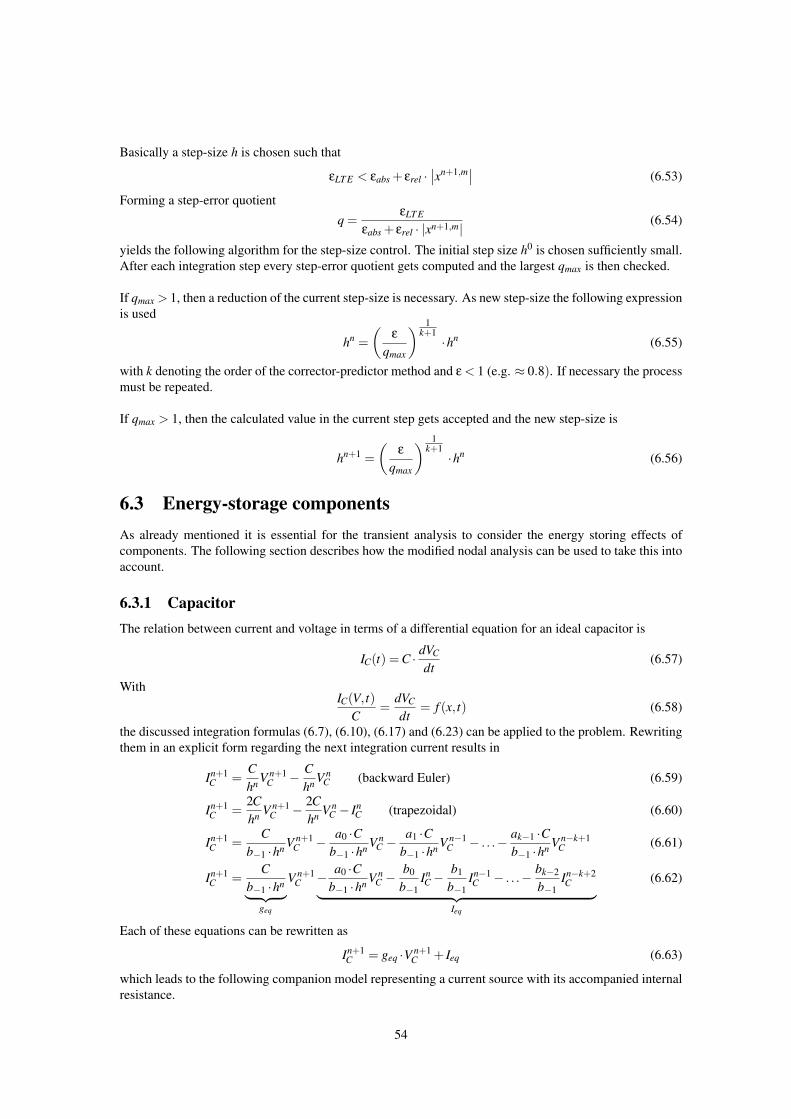
Basically a step-size h is chosen such that
εLT E < εabs + εrel ·∣∣xn+1,m∣∣ (6.53)
Forming a step-error quotientq =
εLT E
εabs + εrel · |xn+1,m|(6.54)
yields the following algorithm for the step-size control. The initial step size h0 is chosen sufficiently small.After each integration step every step-error quotient gets computed and the largest qmax is then checked.
If qmax > 1, then a reduction of the current step-size is necessary. As new step-size the following expressionis used
hn =(
ε
qmax
) 1k+1·hn (6.55)
with k denoting the order of the corrector-predictor method and ε < 1 (e.g. ≈ 0.8). If necessary the processmust be repeated.
If qmax > 1, then the calculated value in the current step gets accepted and the new step-size is
hn+1 =(
ε
qmax
) 1k+1·hn (6.56)
6.3 Energy-storage componentsAs already mentioned it is essential for the transient analysis to consider the energy storing effects ofcomponents. The following section describes how the modified nodal analysis can be used to take this intoaccount.
6.3.1 CapacitorThe relation between current and voltage in terms of a differential equation for an ideal capacitor is
IC(t) = C · dVC
dt(6.57)
WithIC(V, t)
C=
dVC
dt= f (x, t) (6.58)
the discussed integration formulas (6.7), (6.10), (6.17) and (6.23) can be applied to the problem. Rewritingthem in an explicit form regarding the next integration current results in
In+1C =
Chn V n+1
C − Chn V n
C (backward Euler) (6.59)
In+1C =
2Chn V n+1
C − 2Chn V n
C − InC (trapezoidal) (6.60)
In+1C =
Cb−1 ·hn V n+1
C − a0 ·Cb−1 ·hn V n
C −a1 ·C
b−1 ·hn V n−1C − . . .− ak−1 ·C
b−1 ·hn V n−k+1C (6.61)
In+1C =
Cb−1 ·hn︸ ︷︷ ︸
geq
V n+1C − a0 ·C
b−1 ·hn V nC −
b0
b−1InC−
b1
b−1In−1C − . . .− bk−2
b−1In−k+2C︸ ︷︷ ︸
Ieq
(6.62)
Each of these equations can be rewritten as
In+1C = geq ·V n+1
C + Ieq (6.63)
which leads to the following companion model representing a current source with its accompanied internalresistance.
54
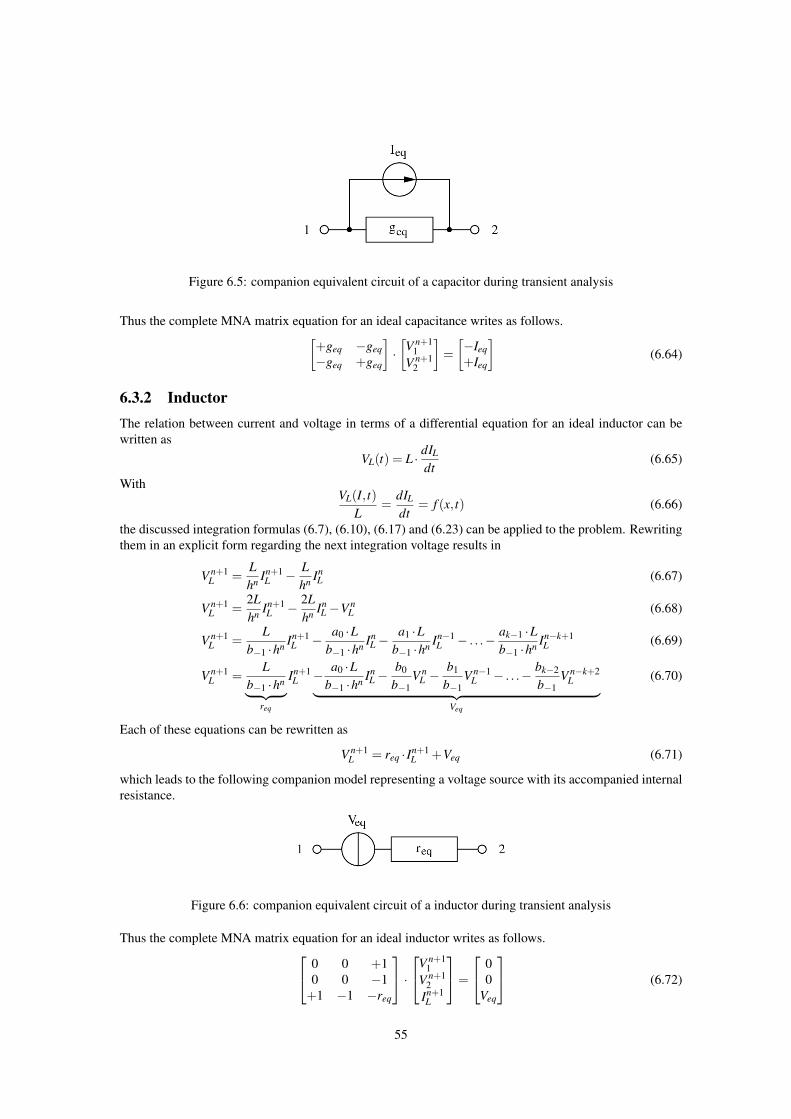
Figure 6.5: companion equivalent circuit of a capacitor during transient analysis
Thus the complete MNA matrix equation for an ideal capacitance writes as follows.[+geq −geq−geq +geq
]·[V n+1
1V n+1
2
]=[−Ieq+Ieq
](6.64)
6.3.2 InductorThe relation between current and voltage in terms of a differential equation for an ideal inductor can bewritten as
VL(t) = L · dIL
dt(6.65)
WithVL(I, t)
L=
dIL
dt= f (x, t) (6.66)
the discussed integration formulas (6.7), (6.10), (6.17) and (6.23) can be applied to the problem. Rewritingthem in an explicit form regarding the next integration voltage results in
V n+1L =
Lhn In+1
L − Lhn In
L (6.67)
V n+1L =
2Lhn In+1
L − 2Lhn In
L−V nL (6.68)
V n+1L =
Lb−1 ·hn In+1
L − a0 ·Lb−1 ·hn In
L−a1 ·L
b−1 ·hn In−1L − . . .− ak−1 ·L
b−1 ·hn In−k+1L (6.69)
V n+1L =
Lb−1 ·hn︸ ︷︷ ︸
req
In+1L − a0 ·L
b−1 ·hn InL−
b0
b−1V n
L −b1
b−1V n−1
L − . . .− bk−2
b−1V n−k+2
L︸ ︷︷ ︸Veq
(6.70)
Each of these equations can be rewritten as
V n+1L = req · In+1
L +Veq (6.71)
which leads to the following companion model representing a voltage source with its accompanied internalresistance.
Figure 6.6: companion equivalent circuit of a inductor during transient analysis
Thus the complete MNA matrix equation for an ideal inductor writes as follows. 0 0 +10 0 −1
+1 −1 −req
·V n+1
1V n+1
2In+1L
=
00
Veq
(6.72)
55
It is also possible to model the ideal inductor as a current source with an internal resistance which wouldyield a similar equivalent circuit as for the capacitor. But with the proposed model it is possible to usealike computation schemes for capacitors and inductors. Charges become flues, capacitances become in-ductances and finally voltages become currents and the other way around. Everything else (especially thecoeffcients in the integration formulas) can be reused.
6.3.3 Coupled InductorsIn a non-ideal transformer, there are two (or more) coupled inductors. The model for the transient simula-tion is not very different from the one of a single inductor. In addition to each coil, the mutal inductancehas to be counted for.
VL1 = L1 ·dIL1
dt+M12 ·
dIL2
dt+ IL1 ·R1 (6.73)
with M12 = k ·√
L1 ·L2 (6.74)and R1 ohmic resistance of coil 1 (6.75)
So it is:
V n+1L1 = req11 · In+1
L1 + req12 · In+1L2 +Veq(In
L1, InL2, ...) (6.76)
Note that req11 includes the ohmic resistance R1. For backward Euler, it therefore follows:
V n+1L1 =
(L1
hn +R1
)︸ ︷︷ ︸
req11
· In+1L1 +
k ·√
L1 ·L2
hn︸ ︷︷ ︸req12
· In+1L2 −
(L1
hn +R1
)· In
L1−k ·√
L1 ·L2
hn · InL2︸ ︷︷ ︸
Veq1
(6.77)
The voltage across the secondary coil V n+1L2 goes likewise by just changing the indices. Finally, the MNA
matrix writes (port numbers are according to figure 9.2):0 0 0 0 +1 00 0 0 0 0 +10 0 0 0 0 −10 0 0 0 −1 0
+1 0 0 −1 −req11 −req120 +1 −1 0 −req21 −req22
·
V n+11
V n+12
V n+13
V n+14
In+1L1
In+1L2
=
0000
Veq1Veq2
(6.78)
These equations can also give an idea on how to model more than two coupled inductors. For three coupledinductors, the voltage across coil 1 writes:
VL1 = L1 ·dIL1
dt+M12 ·
dIL2
dt+M13 ·
dIL3
dt+ IL1 ·R1 (6.79)
VL2 = L2 ·dIL2
dt+M12 ·
dIL1
dt+M23 ·
dIL3
dt+ IL2 ·R2 (6.80)
VL3 = L3 ·dIL3
dt+M13 ·
dIL1
dt+M23 ·
dIL2
dt+ IL3 ·R3 (6.81)
with M12 = k12 ·√
L1 ·L2 (6.82)
and M13 = k13 ·√
L1 ·L3 (6.83)
and M23 = k23 ·√
L2 ·L3 (6.84)
This can be easily extended to an arbitrary number of coupled inductors.
56
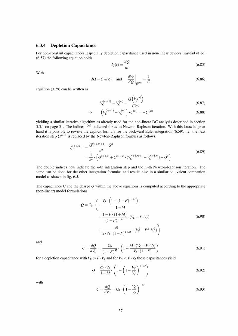
6.3.4 Depletion CapacitanceFor non-constant capacitances, especially depletion capacitance used in non-linear devices, instead of eq.(6.57) the following equation holds.
IC(t) =dQdt
(6.85)
With
dQ = C ·dVC anddVC
dQ
∣∣∣∣Q(m)
=1C
(6.86)
equation (3.29) can be written as
V (m+1)C = V (m)
C −Q(
V (m)C
)C(m) (6.87)
⇒(
V (m+1)C −V (m)
C
)·C(m) =−Q(m) (6.88)
yielding a similar iterative algorithm as already used for the non-linear DC analysis described in section3.3.1 on page 31. The indices (m) indicated the m-th Newton-Raphson iteration. With this knowledge athand it is possible to rewrite the explicit formula for the backward Euler integration (6.59), i.e. the nextiteration step Qm+1 is replaced by the Newton-Raphson formula as follows.
In+1,m+1C =
Qn+1,m+1−Qn
hn
=1hn ·
(Qn+1,m +Cn+1,m ·(V n+1,m+1
C −V n+1,mC )−Qn
) (6.89)
The double indices now indicate the n-th integration step and the m-th Newton-Raphson iteration. Thesame can be done for the other integration formulas and results also in a similar equivalent companionmodel as shown in fig. 6.5.
The capacitance C and the charge Q within the above equations is computed according to the appropriate(non-linear) model formulations.
Q = C0 ·
(+
VJ ·(
1− (1−F)1−M)
1−M
+1−F · (1+M)
(1−F)1+M · (VC−F ·VJ)
+M
2 ·VJ · (1−F)1+M ·(V 2
C −F2 ·V 2J))
(6.90)
and
C =dQdVC
=C0
(1−F)M ·(
1+M · (VC−F ·VJ)
VJ · (1−F)
)(6.91)
for a depletion capacitance with VC > F ·VJ and for VC < F ·VJ those capacitances yield
Q =C0 ·VJ
1−M·
(1−(
1− VC
VJ
)1−M)
(6.92)
with
C =dQdVC
= C0 ·(
1− VC
VJ
)−M
(6.93)
57
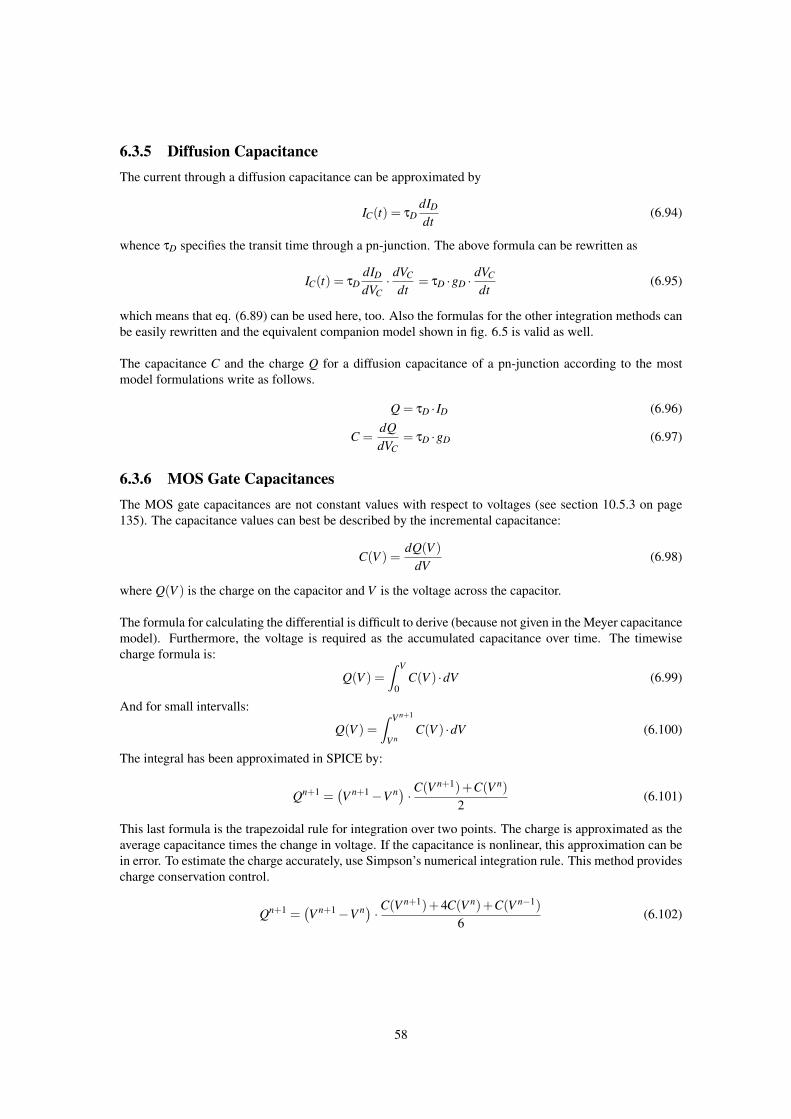
6.3.5 Diffusion CapacitanceThe current through a diffusion capacitance can be approximated by
IC(t) = τDdID
dt(6.94)
whence τD specifies the transit time through a pn-junction. The above formula can be rewritten as
IC(t) = τDdID
dVC· dVC
dt= τD ·gD ·
dVC
dt(6.95)
which means that eq. (6.89) can be used here, too. Also the formulas for the other integration methods canbe easily rewritten and the equivalent companion model shown in fig. 6.5 is valid as well.
The capacitance C and the charge Q for a diffusion capacitance of a pn-junction according to the mostmodel formulations write as follows.
Q = τD · ID (6.96)
C =dQdVC
= τD ·gD (6.97)
6.3.6 MOS Gate CapacitancesThe MOS gate capacitances are not constant values with respect to voltages (see section 10.5.3 on page135). The capacitance values can best be described by the incremental capacitance:
C(V ) =dQ(V )
dV(6.98)
where Q(V ) is the charge on the capacitor and V is the voltage across the capacitor.
The formula for calculating the differential is difficult to derive (because not given in the Meyer capacitancemodel). Furthermore, the voltage is required as the accumulated capacitance over time. The timewisecharge formula is:
Q(V ) =Z V
0C(V ) ·dV (6.99)
And for small intervalls:
Q(V ) =Z V n+1
V nC(V ) ·dV (6.100)
The integral has been approximated in SPICE by:
Qn+1 =(V n+1−V n) ·C(V n+1)+C(V n)
2(6.101)
This last formula is the trapezoidal rule for integration over two points. The charge is approximated as theaverage capacitance times the change in voltage. If the capacitance is nonlinear, this approximation can bein error. To estimate the charge accurately, use Simpson’s numerical integration rule. This method providescharge conservation control.
Qn+1 =(V n+1−V n) ·C(V n+1)+4C(V n)+C(V n−1)
6(6.102)
58
6.4 Special time-domain models
6.4.1 AM modulated AC sourceAn AC voltage source in the time-domain is characterized by its frequency f , the initial phase φ and theamplitude A. During amplitude modulation the modulation level M must be considered. The output voltageof the source is determined by the following equation.
V1 (t)−V2 (t) = (1+M ·V3 (t)) ·A · sin(ω · t +φ) (6.103)
Figure 6.7: AM modulated AC source
The appropriate MNA matrix entries during the transient analysis decribing a simple linear operation canbe written as
. . . 1
. . . −1
. . . 01 −1 −M ·A · sin(ω · t +φ) 0
·
V1 (t)V2 (t)V3 (t)J1 (t)
=
I1 (t)I2 (t)I3 (t)
A · sin(ω · t +φ)
(6.104)
6.4.2 PM modulated AC sourceThe phase modulated AC source is also characterized by the frequency f , the amplidude A and by an initialphase φ. The output voltage in the time-domain is determinded by the following equation
V1 (t)−V2 (t) = A · sin(ω · t +φ+M ·V3 (t)) (6.105)
whereas M denotes the modulation index and V3 the modulating voltage.
Figure 6.8: PM modulated AC source
The component is non-linear in the frequency- as well in the time-domain. In order to prepare the sourcefor subsequent Newton-Raphson iterations the derivative
g =∂(V1−V2)
∂V3= M ·A · cos(ω · t +φ+M ·V3) (6.106)
is required. With this at hand the MNA matrix entries of the PM modulated AC voltage source during thetransient analysis can be written as
. . . +1
. . . −1
. . . 0+1 −1 g 0
·
V1 (t)V2 (t)V3 (t)J1 (t)
=
I1 (t)I2 (t)I3 (t)
g ·V3−A · sin(ω · t +φ+M ·V3)
(6.107)
59
6.5 Components defined in the frequency domainThe time-domain simulation of components defined in the frequency-domain can be performed using aninverse Fourier transformation of the Y-parameters of the component (giving the impulse response) and anadjacent convolution with the prior node voltages (or branch currents) of the component.
This requires a memory of the node voltages and branch currents for each component defined in thefrequency-domain. During a transient simulation the time steps are not equidistant and the maximumrequired memory length Tend of a component may not correspond with the time grid produced by the timestep control (see section 6.2.3 on page 53) of the transient simulation. That is why an interpolation of exactvalues (voltage or current) at a given point in time is necessary.
Components defined in the frequency-domain can be divided into two major classes.
• Components with frequency-independent (non-dispersive) delay times and with or without constantlosses.
• Components with frequency-dependent (dispersive) delay times and losses.
6.5.1 Components with frequency-independent delay timesComponents with constant delay times are a special case. The impulse response corresponds to the nodevoltages and/or branch currents at some prior point in time optionally multiplied with a constant loss factor.
Voltage controlled current source
With no constant delay time the MNA matrix entries of a voltage controlled current source is determinedby the following equations according to the node numbering in fig. 9.8 on page 96.
I2 =−I3 = G · (V1−V4) (6.108)
The equations yield the following MNA entries during the transient analysis.0 0 0 0
+G 0 0 −G−G 0 0 +G0 0 0 0
·
V1V2V3V4
=
I1I2I3I4
(6.109)
With a constant delay time τ eq. (6.108) rewrites as
I2 (t) =−I3 (t) = G · (V1 (t− τ)−V4 (t− τ)) (6.110)
which yields the following MNA entries during the transient analysis.0 0 0 00 0 0 00 0 0 00 0 0 0
·
V1 (t)V2 (t)V3 (t)V4 (t)
=
I1 (t)
−G · (V1 (t− τ)−V4 (t− τ))+G · (V1 (t− τ)−V4 (t− τ))
I4 (t)
(6.111)
Voltage controlled voltage source
The MNA matrix entries of a voltage controlled voltage source are determined by the following character-istic equation according to the node numbering in fig. 9.10 on page 98.
V2−V3 = G · (V4−V1) (6.112)
60
This equation yields the following augmented MNA matrix entries with a single extra branch equation.0 0 0 0 00 0 0 0 −10 0 0 0 10 0 0 0 0G −1 1 −G 0
·
V1V2V3V4J1
=
I1I2I3I40
(6.113)
When considering an additional constant time delay τ eq. (6.112) must be rewritten as
V2 (t)−V3 (t) = G · (V4 (t− τ)−V1 (t− τ)) (6.114)
This representation requires a change of the MNA matrix entries which now yield the following matrixequation.
0 0 0 0 00 0 0 0 −10 0 0 0 10 0 0 0 00 −1 1 0 0
·
V1 (t)V2 (t)V3 (t)V4 (t)J1 (t)
=
I1 (t)I2 (t)I3 (t)I4 (t)
G · (V4 (t− τ)−V1 (t− τ))
(6.115)
Current controlled current source
With no time delay the MNA matrix entries of a current controlled current source are determined by thefollowing equations according to the node numbering in fig. 9.9 on page 97.
I2 =−I3 = G · I1 =−G · I4 (6.116)V1 = V4 (6.117)
These equations yield the following MNA matrix entries using a single extra branch equation.0 0 0 0 1/G0 0 0 0 10 0 0 0 −10 0 0 0 −1/G1 0 0 −1 0
·
V1V2V3V4J1
=
I1I2I3I40
(6.118)
When additional considering a constant delay time τ eq. (6.116) must be rewritten as
I2 (t) =−I3 (t) = G · I1 (t− τ) =−G · I4 (t− τ) (6.119)
Thus the MNA matrix entries change as well yielding0 0 0 0 10 0 0 0 00 0 0 0 00 0 0 0 −11 0 0 −1 0
·
V1 (t)V2 (t)V3 (t)V4 (t)J1 (t)
=
I1 (t)
−G ·J1 (t− τ)+G ·J1 (t− τ)
I4 (t)0
(6.120)
Current controlled voltage source
The MNA matrix entries for a current controlled voltage source are determined by the following character-istic equations according to the node numbering in fig. 9.11 on page 98.
V2−V3 = G · I2 =−G · I3 (6.121)V1 = V4 (6.122)
61
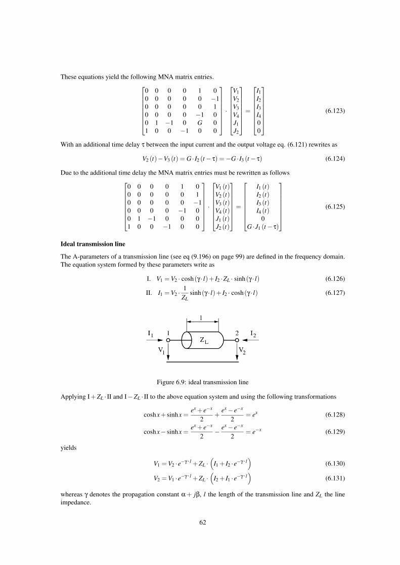
These equations yield the following MNA matrix entries.0 0 0 0 1 00 0 0 0 0 −10 0 0 0 0 10 0 0 0 −1 00 1 −1 0 G 01 0 0 −1 0 0
·
V1V2V3V4J1J2
=
I1I2I3I400
(6.123)
With an additional time delay τ between the input current and the output voltage eq. (6.121) rewrites as
V2 (t)−V3 (t) = G · I2 (t− τ) =−G · I3 (t− τ) (6.124)
Due to the additional time delay the MNA matrix entries must be rewritten as follows0 0 0 0 1 00 0 0 0 0 10 0 0 0 0 −10 0 0 0 −1 00 1 −1 0 0 01 0 0 −1 0 0
·
V1 (t)V2 (t)V3 (t)V4 (t)J1 (t)J2 (t)
=
I1 (t)I2 (t)I3 (t)I4 (t)
0G ·J1 (t− τ)
(6.125)
Ideal transmission line
The A-parameters of a transmission line (see eq (9.196) on page 99) are defined in the frequency domain.The equation system formed by these parameters write as
I. V1 = V2 · cosh(γ · l)+ I2 ·ZL · sinh(γ · l) (6.126)
II. I1 = V2 ·1
ZLsinh(γ · l)+ I2 · cosh(γ · l) (6.127)
Figure 6.9: ideal transmission line
Applying I+ZL · II and I−ZL · II to the above equation system and using the following transformations
coshx+ sinhx =ex + e−x
2+
ex− e−x
2= ex (6.128)
coshx− sinhx =ex + e−x
2− ex− e−x
2= e−x (6.129)
yields
V1 = V2 ·e−γ· l +ZL ·(
I1 + I2 ·e−γ· l)
(6.130)
V2 = V1 ·e−γ· l +ZL ·(
I2 + I1 ·e−γ· l)
(6.131)
whereas γ denotes the propagation constant α + jβ, l the length of the transmission line and ZL the lineimpedance.
62
These equations can be transformed from the frequency domain into the time domain using the inverseFourier transformation. The frequency independent loss α 6= f (ω) gives the constant factor
A = e−α· l (6.132)
The only remaining frequency dependent term is
e− jβ· l = e− jω·τ with β =ω
vph=
ω
c0=
ω ·τl
(6.133)
which yields the following transformation
f (ω) ·e−γ· l = A · f (ω) ·e− jω·τ⇐⇒ A · f (t− τ) (6.134)
All the presented time-domain models with a frequency-independent delay time are based on this simpletransformation. It can be applied since the phase velocity vph 6= f (ω) is not a function of the frequency.This is true for all non-dispersive transmission media, e.g. air or vacuum. The given transformation cannow be applied to the eq. (6.130) and eq. (6.131) defined in the frequency-domain to obtain equations inthe time-domain.
The length Tend of the memory needed by the ideal transmission line can be easily computed by
Tend = τ =l
vph=
lc0
(6.135)
whereas c0 denotes the speed of light in free space (since there is no dielectric involved during transmission)and l the physical length of the transmission line.
The MNA matrix for a lossy (or lossless with α = 0) transmission line during the transient analysis isaugmented by two new rows and columns in order to consider the following branch equations.
V1 (t) = ZL · I1 (t)+A · (ZL · I2 (t− τ)+V2 (t− τ)) (6.136)V2 (t) = ZL · I2 (t)+A · (ZL · I1 (t− τ)+V1 (t− τ)) (6.137)
Thus the MNA matrix entries can be written as0 0 1 00 0 0 11 0 −ZL 00 1 0 −ZL
·
V1 (t)V2 (t)J1 (t)J2 (t)
=
I1 (t)I2 (t)
A · (V2 (t− τ)+ZL ·J2 (t− τ))A · (V1 (t− τ)+ZL ·J1 (t− τ))
(6.138)
with A denoting the loss factor derived from the constant (and frequency independent) line attenuation α
and the transmission line length l.
A = e−α
2 · l (6.139)
Ideal 4-terminal transmission line
The ideal 4-terminal transmission line is a two-port as well. It differs from the 2-terminal line as shown infig. 6.5.1 in two new node voltages and branch currents.
63
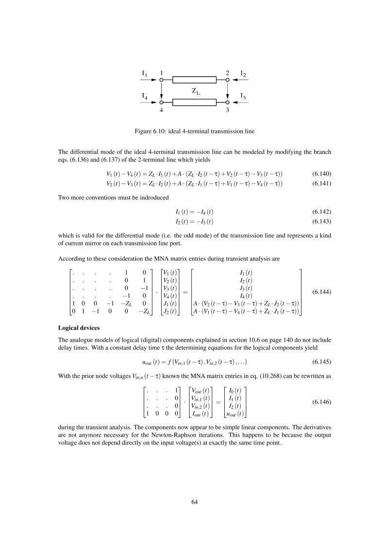
Figure 6.10: ideal 4-terminal transmission line
The differential mode of the ideal 4-terminal transmission line can be modeled by modifying the brancheqs. (6.136) and (6.137) of the 2-terminal line which yields
V1 (t)−V4 (t) = ZL · I1 (t)+A · (ZL · I2 (t− τ)+V2 (t− τ)−V3 (t− τ)) (6.140)V2 (t)−V3 (t) = ZL · I2 (t)+A · (ZL · I1 (t− τ)+V1 (t− τ)−V4 (t− τ)) (6.141)
Two more conventions must be indroduced
I1 (t) =−I4 (t) (6.142)I2 (t) =−I3 (t) (6.143)
which is valid for the differential mode (i.e. the odd mode) of the transmission line and represents a kindof current mirror on each transmission line port.
According to these consideration the MNA matrix entries during transient analysis are. . . . 1 0. . . . 0 1. . . . 0 −1. . . . −1 01 0 0 −1 −ZL 00 1 −1 0 0 −ZL
·
V1 (t)V2 (t)V3 (t)V4 (t)J1 (t)J2 (t)
=
I1 (t)I2 (t)I3 (t)I4 (t)
A · (V2 (t− τ)−V3 (t− τ)+ZL ·J2 (t− τ))A · (V1 (t− τ)−V4 (t− τ)+ZL ·J1 (t− τ))
(6.144)
Logical devices
The analogue models of logical (digital) components explained in section 10.6 on page 140 do not includedelay times. With a constant delay time τ the determining equations for the logical components yield
uout (t) = f (Vin,1 (t− τ) ,Vin,2 (t− τ) , . . .) (6.145)
With the prior node voltages Vin,n (t− τ) known the MNA matrix entries in eq. (10.268) can be rewritten as. . . 1. . . 0. . . 01 0 0 0
·
Vout (t)Vin,1 (t)Vin,2 (t)Iout (t)
=
I0 (t)I1 (t)I2 (t)
uout (t)
(6.146)
during the transient analysis. The components now appear to be simple linear components. The derivativesare not anymore necessary for the Newton-Raphson iterations. This happens to be because the outputvoltage does not depend directly on the input voltage(s) at exactly the same time point.
64
6.5.2 Components with frequency-dependent delay times and lossesIn the general case a component with P ports which is defined in the frequency-domain can be representedby the following matrix equation.
Y11 Y12 . . . Y1PY21 Y22 Y2P
.... . .
...YP1 YP2 . . . YPP
·
V1V2...
VP
=
I1I2...
IP
(6.147)
This matrix representation is the MNA representation during the AC analysis. With no specific time-domainmodel at hand the equation [
Y ( jω)]·[V ( jω)
]=[I ( jω)
](6.148)
must be transformed into the time-domain using a Fourier transformation.
The convolution integral
The multiplication in the frequency-domain is equivalent to a convolution in the time-domain after thetransformation. It yields the following matrix equation[
H (t)]∗[V (t)
]=[I (t)
](6.149)
whereas H (t) is the impulse response based on the frequency-domain model and the ∗ operator denotesthe convolution integral
H (t)∗V (t) =Z +∞
−∞
H (τ) ·V (t− τ)dτ (6.150)
The lower bound of the given integral is set to zero since both the impulse response as well as the nodevoltages are meant to deliver no contribution to the integral. Otherwise the circuit appears to be unphysical.The upper limit should be bound to a maximum impulse response time Tend
H (t)∗V (t) =Z Tend
0H (τ) ·V (t− τ)dτ (6.151)
withH (τ) = 0 ∀ τ > Tend (6.152)
Since there is no analytic represention for the impulse response as well as for the node voltages eq. (6.151)must be rewritten to
H (n ·∆t)∗V (n ·∆t) =N−1
∑k=0
H (k ·∆t) ·V ((n− k) ·∆t) (6.153)
with∆t =
Tend
N(6.154)
whereas N denotes the number of samples to be used during numerical convolution. Using the current timestep t = n ·∆t it is possible to express eq. (6.153) as
I (t) = H (0) ·V (t)+N−1
∑k=1
H (k ·∆t) ·V (t− k ·∆t)︸ ︷︷ ︸Ieq
(6.155)
With G = H (0) the resulting MNA matrix equation during the transient analysis gets[G]·[V (t)
]=[I (t)
]−[Ieq]
(6.156)
65
This means, the component defined in the frequency-domain can be expressed with an equivalent DCadmittance G and additional independent current sources in the time-domain. Each independent currentsource at node r delivers the following current
Ieqr =P
∑c=1
N−1
∑k=1
Hrc (k ·∆t) ·Vc (t− k ·∆t) (6.157)
whereas Vc denotes the node voltage at node c at some prior time and Hrc the impulse response of thecomponent based on the frequency-domain representation. The MNA matrix equation during transientanalysis can thus be written as
G11 G12 . . . G1PG21 G22 G2P
.... . .
...GP1 GP2 . . . GPP
·
V1 (t)V2 (t)
...VP (t)
=
I1 (t)I2 (t)
...IP (t)
−
Ieq1
Ieq2...
IeqP
(6.158)
Frequency- to time-domain transformation
With the number of samples N being a power of two it is possible to use the Inverse Fast Fourier Transfor-mation (IFFT). The transformation to be performed is
Y ( jω)⇔ H (t) (6.159)
The maximum impulse response time of the component is specified by Tend requiring the following trans-formation pairs.
Y ( jωi)⇔ H (ti) with i = 0,1,2, . . . ,N−1 (6.160)
with
ti = 0,∆t,2 ·∆t, . . . ,(N−1) ·∆t (6.161)
ωi = 0,1
Tend,
1Tend
, . . . ,N/2Tend
(6.162)
The frequency samples in eq. (6.162) indicate that only half the values are required to obtain the appropriateimpulse response. This is because the impulse response H (t) is real valued and that is why
Y ( jω) = Y ∗ (− jω) (6.163)
The maximum frequency considered is determined by the maximum impulse response time Tend and thenumber of time samples N.
fmax =N/2
2π ·Tend=
14π ·∆t
(6.164)
It could prove useful to weight the Y-parameter samples in the frequency-domain by multiplying them withan appropriate windowing function (e.g. Kaiser-Bessel).
Implementation considerations
For the method presented the Y-parameters of a component must be finite for f → 0 as well as for f → fmax.To obtain G = H (0) the Y-parameters at f = 0 are required. This cannot be ensured for the general case(e.g. for an ideal inductor).
66
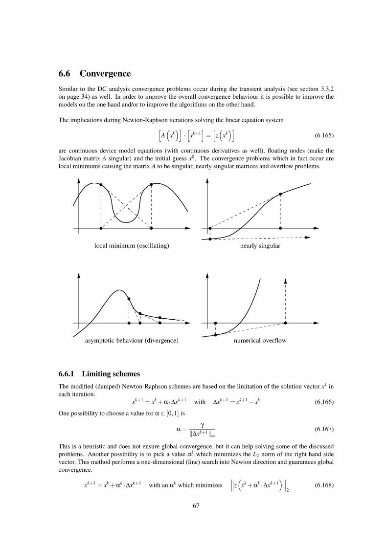
6.6 ConvergenceSimilar to the DC analysis convergence problems occur during the transient analysis (see section 3.3.2on page 34) as well. In order to improve the overall convergence behaviour it is possible to improve themodels on the one hand and/or to improve the algorithms on the other hand.
The implications during Newton-Raphson iterations solving the linear equation system[A(
xk)]·[xk+1
]=[z(
xk)]
(6.165)
are continuous device model equations (with continuous derivatives as well), floating nodes (make theJacobian matrix A singular) and the initial guess x0. The convergence problems which in fact occur arelocal minimums causing the matrix A to be singular, nearly singular matrices and overflow problems.
6.6.1 Limiting schemesThe modified (damped) Newton-Raphson schemes are based on the limitation of the solution vector xk ineach iteration.
xk+1 = xk +α ·∆xk+1 with ∆xk+1 = xk+1− xk (6.166)
One possibility to choose a value for α ∈ [0,1] is
α =γ
‖∆xk+1‖∞
(6.167)
This is a heuristic and does not ensure global convergence, but it can help solving some of the discussedproblems. Another possibility is to pick a value αk which minimizes the L2 norm of the right hand sidevector. This method performs a one-dimensional (line) search into Newton direction and guarantees globalconvergence.
xk+1 = xk +αk ·∆xk+1 with an α
k which minimizes∥∥∥z(
xk +αk ·∆xk+1
)∥∥∥2
(6.168)
67
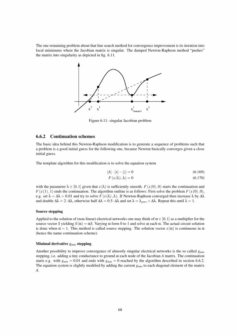
The one remaining problem about that line search method for convergence improvement is its iteration intolocal minimums where the Jacobian matrix is singular. The damped Newton-Raphson method “pushes”the matrix into singularity as depicted in fig. 6.11.
Figure 6.11: singular Jacobian problem
6.6.2 Continuation schemesThe basic idea behind this Newton-Raphson modification is to generate a sequence of problems such thata problem is a good initial guess for the following one, because Newton basically converges given a closeinitial guess.
The template algorithm for this modification is to solve the equation system
[A] · [x]− [z] = 0 (6.169)F (x(λ) ,λ) = 0 (6.170)
with the parameter λ ∈ [0,1] given that x(λ) is sufficiently smooth. F (x(0) ,0) starts the continuation andF (x(1) ,1) ends the continuation. The algorithm outline is as follows: First solve the problem F (x(0) ,0),e.g. set λ = ∆λ = 0.01 and try to solve F (x(λ) ,λ). If Newton-Raphson converged then increase λ by ∆λ
and double ∆λ = 2 ·∆λ, otherwise half ∆λ = 0.5 ·∆λ and set λ = λprev +∆λ. Repeat this until λ = 1.
Source stepping
Applied to the solution of (non-linear) electrical networks one may think of α∈ [0,1] as a multiplier for thesource vector S yielding S (α) = αS. Varying α form 0 to 1 and solve at each α. The actual circuit solutionis done when α = 1. This method is called source stepping. The solution vector x(α) is continuous in α
(hence the name continuation scheme).
Minimal derivative gmin stepping
Another possibility to improve convergence of almostly singular electrical networks is the so called gminstepping, i.e. adding a tiny conductance to ground at each node of the Jacobian A matrix. The continuationstarts e.g. with gmin = 0.01 and ends with gmin = 0 reached by the algorithm described in section 6.6.2.The equation system is slightly modified by adding the current gmin to each diagonal element of the matrixA.
68
Chapter 7
Harmonic Balance Analysis
Harmonic balance is a non-linear, frequency-domain, steady-state simulation. The voltage and currentsources create discrete frequencies resulting in a spectrum of discrete frequencies at every node in thecircuit. Linear circuit components are solely modeled in frequency domain. Non-linear components aremodeled in time domain and Fourier-transformed before each solving step. The informations in this chapterare taken from [8] (chapter 3) which is a very nice and well-written publication on this topic.
The harmonic balance simulation is ideal for situations where transient simulation methods are problematic.These are:
• components modeled in frequency domain, for instance (dispersive) transmission lines
• circuit time constants large compared to period of simulation frequency
• circuits with lots of reactive components
Harmonic balance methods, therefore, are the best choice for most microwave circuits excited with sinu-soidal signals (e.g. mixers, power amplifiers).
7.1 The Basic ConceptAs the non-linear elements are still modeled in time domain, the circuit first must be separated into a linearand a non-linear part. The internal impedances Zi of the voltage sources are put into the linear part as well.Figure 7.1 illustrates the concept. Let us define the following symbols:
M = number of (independent) voltage sources
N = number of connections between linear and non-linear subcircuit
K = number of calculated harmonics
L = number of nodes in linear subcircuit
69
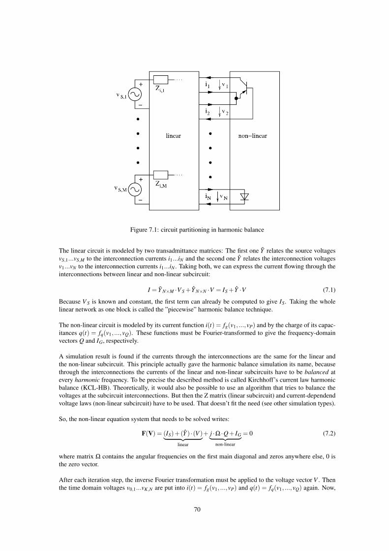
Figure 7.1: circuit partitioning in harmonic balance
The linear circuit is modeled by two transadmittance matrices: The first one Y relates the source voltagesvS,1...vS,M to the interconnection currents i1...iN and the second one Y relates the interconnection voltagesv1...vN to the interconnection currents i1...iN . Taking both, we can express the current flowing through theinterconnections between linear and non-linear subcircuit:
I = Y N×M ·V S + Y N×N ·V = IS + Y ·V (7.1)
Because V S is known and constant, the first term can already be computed to give IS. Taking the wholelinear network as one block is called the ”piecewise” harmonic balance technique.
The non-linear circuit is modeled by its current function i(t) = fg(v1, ...,vP) and by the charge of its capac-itances q(t) = fq(v1, ...,vQ). These functions must be Fourier-transformed to give the frequency-domainvectors Q and IG, respectively.
A simulation result is found if the currents through the interconnections are the same for the linear andthe non-linear subcircuit. This principle actually gave the harmonic balance simulation its name, becausethrough the interconnections the currents of the linear and non-linear subcircuits have to be balanced atevery harmonic frequency. To be precise the described method is called Kirchhoff’s current law harmonicbalance (KCL-HB). Theoretically, it would also be possible to use an algorithm that tries to balance thevoltages at the subcircuit interconnections. But then the Z matrix (linear subcircuit) and current-dependendvoltage laws (non-linear subcircuit) have to be used. That doesn’t fit the need (see other simulation types).
So, the non-linear equation system that needs to be solved writes:
F(V) = (IS)+(Y ) ·(V )︸ ︷︷ ︸linear
+ j ·Ω ·Q+ IG︸ ︷︷ ︸non-linear
= 0 (7.2)
where matrix Ω contains the angular frequencies on the first main diagonal and zeros anywhere else, 0 isthe zero vector.
After each iteration step, the inverse Fourier transformation must be applied to the voltage vector V . Thenthe time domain voltages v0,1...vK,N are put into i(t) = fg(v1, ...,vP) and q(t) = fq(v1, ...,vQ) again. Now,
70
a Fourier transformation gives the vectors Q and IG for the next iteration step. After repeating this severaltimes, a simulation result has hopefully be found.
Having found this result means having got the voltages v1...vN at the interconnections of the two subcircuits.With these values the voltages at all nodes can be calculated: Forget about the non-linear subcircuit, putcurrent sources at the former interconnections (using the calculated values) and perform a normal ACsimulation. After that the simulation is complete.
A short note to the construction of the quantities: One big difference between the HB and the conventionalsimulation types like a DC or an AC simulation is the structure of the matrices and vectors. A vectorused in a conventional simulation contains one value for each node. In an HB simulation there are manyharmonics and thus, a vector contains K values for each node. This means that within a matrix, there is aK×K diagonal submatrix for each node. Using this structure, all equations can be written in the usual way,i.e. without paying attention to the special matrix and vector structure. In a computer program, however, aspecial matrix class is needed in order to not waste memory for the off-diagonal zeros.
7.2 Going through each Step
7.2.1 Creating Transadmittance MatrixIt needs several steps to get the transadmittance matrices [Y ] and [Y ] mentioned in equation (7.1). Firstthe MNA matrix of the linear subcircuit (figure 7.1) is created (chapter 3.1) without the voltage sourcesS1...SM and without the non-linear components. Note that all nodes must appear in the matrix, even thosewhere only non-linear components are connected. Then the transimpedance matrix is derived by excitingone by one the port nodes of the MNA matrix with unity current. After that the transadmittance matrixis calculated by inverting the transimpedance matrix. Finally the matrices [Y ] and [Y ] are filled with thecorresponding elements of the overall transadmittance matrix.
Note: The MNA matrix of the linear subcircuit has L nodes. Every node, that is connected to the non-linearsubcircuit or/and is connected to a voltage source, is called ”port” in the following text. So, there are M +Nports. All these ports need to be differential ones, i.e. without ground reference. Otherwise problemes mayoccur due to singular matrices when calculating [Y ] or [Y ].
Now this should be described in more detail: By use of the MNA matrix [A], the n-th column of thetransimpedance matrix [Z] should be calculated. The voltage source at port n is connected to node i (positiveterminal) and to node j (negative terminal). This results in the following equation. (If port n is referencedto ground, the -1 is simply omitted.)
[A] ·
V1...
VL
=
0...1...−1
...0
← i-th row
← j-th row(7.3)
After having solved it, Z1,n...ZN+M,n are obtained simply by subtraction of the node voltages:
Zm,n = Vk−Vl (7.4)
Here the voltage source at port m is connected to node k (positive terminal) and to node l (negative termi-nal).
71
The next column of [Z] is obtained by changing the right-hand side of equation (7.3) appropriately. As thishas to be done N +M times, it is strongly recommended to use LU decomposition.
As [Y ] is not square, problems encounter by trying to build its inverse matrix. Therefore, the followingprocedure is recommended:
• Create the transimpedance matrix for all ports (sources and interconnections).
• Compute the inverse matrix (transadmittance matrix).
• The upper left and upper right corner contains [Y ] and [Y ].
• The lower left and lower right corner contains the transadmittance matrices to calculate the currentsthrough the sources. They can be used to simplify the AC simulation at the very end.
One further thing must be mentioned: Because the non-linear components and the sources are missing inthe linear MNA matrix, there are often components that are completely disconnected from the rest of thecircuit. The resulting MNA matrix cannot be solved. To avoid this problem, shunt each port with a 100Ω
resistor, i.e. place a resistor in parallel to each non-linear component and to each source. The effect of theseresistors can be easily removed by subtracting 10mS from the first main diagonal of the transadmittancematrix.
7.2.2 Starting ValuesA difficult question is how to find appropriate start values for the harmonic balance simulation. It isrecommended to first perform a DC analysis and start the algorithm with this result. In many situation(perhaps always) an even better starting point can be achieved by also using the result of a linear ACsimulation. However with a large signal strength and strong non-linearities, convergence may still fail.Then, the following procedure might succeed: Perform HB simulation by applying half of the desiredsignal levels. If convergence is reached, the result can be used as start values for the simulation with thefull signal levels. Otherwise the amplitude of the signals can be further decreased in order to repeat theabove-mentioned procedure.
7.2.3 Solution algorithmTo perform a HB simulation, the multi-dimensional, non-linear function 7.2 has to be solved. One of thebest possibilities to do so is the Newton method:
Vn+1 = Vn−JF(Vn)−1 ·F(Vn) (7.5)
⇒ JF(Vn) ·Vn+1 = JF(Vn) ·Vn−F(Vn) (7.6)
with JF being the Jacobian matrix. DC and transient simulation also use this technique, but here a problemappears: The derivatives of the component models are not given in frequency domain. Thus, the Jacobianmust be calculated starting at the HB equation 7.2:
JF(V n) =dF(V )
dV= Y N×N +
∂IG
∂V+ j ·Ω∂Q
∂V= Y N×N + JF,G + j ·Ω ·JF,Q (7.7)
So, two Jacobian matrices have to be built, one for the current IG and one for the charge Q. Both resultedfrom a Fourier Transformation. The two operations (Fourier Transformation and differentiation) are linearand thus, can be exchanged. Hence, the Jacobian matrices are built in time domain and transformed intofrequency domain afterwards.
To obtain a practical algorithm of this procedure, the DFT is best written as matrix equation. By havinga look at equation 15.180 and 15.181, it becomes clear how this works. The harmonic factors exp( jωktn)
72
build the matrix Γ:
DFT: U( jω) = Γ ·u(t) (7.8)
IDFT: u(t) = Γ−1 ·U( jω) (7.9)
with u and U being the vectors of the time and frequency values, respectively. Now, it is possible totransform the desired Jacobian matrix into frequency domain:
JF,G =∂IG
∂V=
∂(Γ · i)∂(Γ ·v)
= Γ · ∂i∂v·Γ−1 (7.10)
Here i is a vector with length K ·N, i.e. first all time values of the first node are inserted, then all time valuesof the second node etc. The Jacobi matrix of i is defined as:
JF,G(u) =
∂i1∂u1
. . .∂i1∂un
.... . .
...∂in∂u1
. . .∂in∂un
(7.11)
Hence this matrix consists of K×K blocks (one for each node) that are diagonal matrices with time valuesof the derivatives in it. (Components exists that create non-diagonal blocks, but these are so special onesthat they do not appear in this document.)
The formula 7.10 seems to be quite clear, but it has to be pointed out how this works with FFT algorithm.With Γ
−1 = (Γ−1)T (see equation 15.181) and (A ·B)T = BT ·AT , it follows:
JF,G = Γ · ∂i∂v·Γ−1 =
(Γ−1 ·
(Γ · ∂i
∂v
)T)T
(7.12)
So, there are two steps to perform an FFT-based transformation of the time domain Jacobian matrix intothe frequency domain Jacobian:
1. Perform an FFT on every column of the Jacobian and build a new matrix A with this result, i.e. thefirst column of A is the FFTed first column of the Jacobian and so on.
2. Perform an IFFT on every row of the matrix A and build a new matrix B with this result, i.e. the firstrow of B is the IFFTed first row of A and so on.
As the Fourier transformation has to be applied to diagonal sub-matrices, the whole above-mentionedprocess can be performed by one single FFT. This is done by taking the ∂i/∂v values in a vector Ji andcalculating:
1K·FFT(Ji) (7.13)
The result is the first column of JF,G. The second column equals the first one rotated down by one element.The third column is the second one rotated down by one element etc. A matrix obeying this structure iscalled Toeplitz matrix.
So, finally the complete HB Newton iteration step can be written down. Putting 7.2 and 7.7 into 7.6 leadsto
JF(Vn) ·Vn+1 = JF,G ·Vn− IG + j ·Ω ·(JF,Q ·Vn−Q)− IS (7.14)
This is important to notice, because many non-linear components cannot be processed at every bias point(see figure 3.5). These components create a new voltage estimate across their nodes, whereas the newestimated absolute voltages at their nodes are not known. Thus, the term JF,G ·Vn can only be created inone single step, leading to the vector IG,J . Luckily, this procedure also saves computation time, as thematrix multiplication need not to be performed. The same is true for the term JF,Q ·Vn, leading to thevector QJ . So it is:
JF ·Vn+1 = IG,J− IG + j ·Ω ·(QJ−Q)− IS (7.15)
73
7.2.4 Termination CriteriaFrequency components with very different magnitude appear in harmonic balance simulation. In order todetect when the solver has found an accurate solution, an absolute as well as relative criteria must be usedon all nodes and at all frequencies. The analysis is regarded as finished if one of the criteria is satisfied.
The absolute and relative criteria write as follows:∣∣In,k + In,k∣∣< εabs ∀ n,k (7.16)
2 ·∣∣∣∣ In,k + In,k
In,k− In,k
∣∣∣∣< εrel ∀ n,k (7.17)
where In,k is the current of the linear circuit partition for node n and frequency k and In,k is the current ofthe non-linear circuit partition.
7.3 A Symbolic HB AlgorithmIn this final section, a harmonic balance algorithm in symbolic language is presented.
Listing 7.1: symbolic HB algorithm
i n i t ( ) ; / / s e p a r a t e l i n e a r and non− l i n e a r d e v i c e sY = c a l c T r a n s M a t r i x ( ) ; / / t r a n s a d m i t t a n c e m a t r i x o f l i n e a r c i r c u i tI s = c a l c S o u r c e C u r r e n t ( ) ; / / s o u r c e c u r r e n t o f l i n e a r s u b c i r c u i t( v , i , q ) = c a l c u l a t e D C ( ) ; / / DC s i m u l a t i o n as i n i t i a l HB e s t i m a t eV = FFT ( v ) ; / / t r a n s f o r m v o l t a g e i n t o f r e q u e n c y domain
l oop :I = FFT ( i ) ; / / c u r r e n t i n t o f r e q u e n c y domainQ = FFT ( q ) ; / / charge i n t o f r e q u e n c y domainE = I s + Y∗V + j ∗Ω∗Q + I ; / / HB e q u a t i o ni f ( abs ( E ) < Eterm ) break ; / / c o n v e r g e n c e reached ?JG = mFFT( GJacob ian ( v ) ) ; / / c r e a t e J a c o b i a n s and t r a n s f o r m . . .JQ = mFFT( QJacob ian ( v ) ) ; / / . . . them i n t o f r e q u e n c y domainJ = Y + j ∗Ω∗JQ + JG ; / / c a l c u l a t e o v e r a l l J a c o b i a nV = V − i n v e r t ( J ) ∗ E ; / / Newton Raphson i t e r a t i o n s t e pv = IFFT (V ) ; / / v o l t a g e i n t o t i m e domaini = n o n l i n e a r C u r r e n t ( v ) ; / / u se component models t o g e t . . .q = n o n l i n e a r C h a r g e ( v ) ; / / . . . v a l u e s f o r n e x t i t e r a t i o ngoto l oop ;
Va = i n v e r t ( Ya ) ∗ I a ; / / AC s i m u l a t i o n t o g e t a l l v o l t a g e s
7.4 Large-Signal S-Parameter SimulationUsing harmonic balance techniques, it is also possible to perform an S-parameter simulation in the large-signal regime. This is called LSSP (large-signal s-parameter). Figure 7.2 shows the principle. The portn excites the circuit with the simulation frequency f0; meanwhile the power of all other ports is set tozero. Having voltage and current of the fundamental frequency f0 at the ports, the S-parameters can becalculated:
Smn =Um( f0)− Im( f0) ·Zm
Un( f0)+ In( f0) ·Zn·√
Zn
Zm(7.18)
74
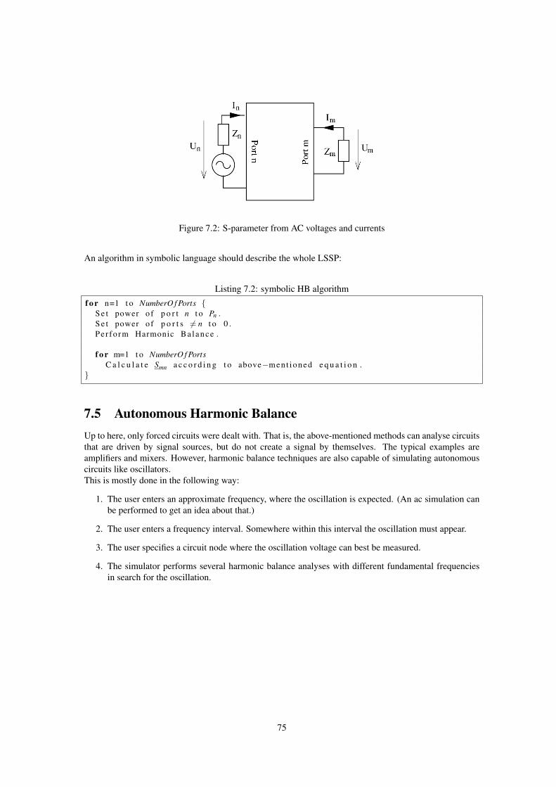
Figure 7.2: S-parameter from AC voltages and currents
An algorithm in symbolic language should describe the whole LSSP:
Listing 7.2: symbolic HB algorithm
f o r n=1 t o NumberO f Ports S e t power o f p o r t n t o Pn .S e t power o f p o r t s 6= n t o 0 .Per fo rm Harmonic Ba lance .
f o r m=1 t o NumberO f PortsC a l c u l a t e Smn a c c o r d i n g t o above−ment ioned e q u a t i o n .
7.5 Autonomous Harmonic BalanceUp to here, only forced circuits were dealt with. That is, the above-mentioned methods can analyse circuitsthat are driven by signal sources, but do not create a signal by themselves. The typical examples areamplifiers and mixers. However, harmonic balance techniques are also capable of simulating autonomouscircuits like oscillators.This is mostly done in the following way:
1. The user enters an approximate frequency, where the oscillation is expected. (An ac simulation canbe performed to get an idea about that.)
2. The user enters a frequency interval. Somewhere within this interval the oscillation must appear.
3. The user specifies a circuit node where the oscillation voltage can best be measured.
4. The simulator performs several harmonic balance analyses with different fundamental frequenciesin search for the oscillation.
75
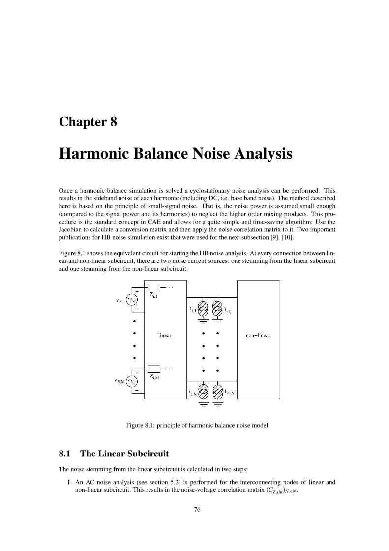
Chapter 8
Harmonic Balance Noise Analysis
Once a harmonic balance simulation is solved a cyclostationary noise analysis can be performed. Thisresults in the sideband noise of each harmonic (including DC, i.e. base band noise). The method describedhere is based on the principle of small-signal noise. That is, the noise power is assumed small enough(compared to the signal power and its harmonics) to neglect the higher order mixing products. This pro-cedure is the standard concept in CAE and allows for a quite simple and time-saving algorithm: Use theJacobian to calculate a conversion matrix and then apply the noise correlation matrix to it. Two importantpublications for HB noise simulation exist that were used for the next subsection [9], [10].
Figure 8.1 shows the equivalent circuit for starting the HB noise analysis. At every connection between lin-ear and non-linear subcircuit, there are two noise current sources: one stemming from the linear subcircuitand one stemming from the non-linear subcircuit.
Figure 8.1: principle of harmonic balance noise model
8.1 The Linear SubcircuitThe noise stemming from the linear subcircuit is calculated in two steps:
1. An AC noise analysis (see section 5.2) is performed for the interconnecting nodes of linear andnon-linear subcircuit. This results in the noise-voltage correlation matrix (CZ,lin)N×N .
76
2. The matrix (CZ,lin)N×N is converted into a noise-current correlation matrix (see section 2.4.2):
(CY,lin)N×N = Y ·CZ,lin ·Y+ (8.1)
where Y is taken from equation 7.2.
Remark: If no explicit noise sources exist in the linear subcircuit, (CZ,lin)N×N can be computed much fasterby using Bosma’s theorem (equation 2.38).
8.2 The Non-Linear SubcircuitThe noise in the non-linear part of the circuit is calculated by using the quasi-static approach, i.e. for everymoment in time the voltages and currents are regarded as a time-dependend bias point. The noise propertiesof these bias points are used for the noise calculation.
Remark: It is not clear whether this approach creates a valid result for noise with long-time correlation(e.g. 1/f noise), too. But up to now, no other methods were proposed and some publications reported tohave achieved reasonable results with this approach and 1/f noise.
Calculating the noise-current correlation matrix (CY,nl)N×N needs several steps. The DC bias point takenfrom the result of the HB simulation is the beginning. Its values are the bias used to build the correlationmatrix (CY,DC). Each part is a K×K diagonal submatrix. The values are the power-spectral densities (PSD)for each harmonic frequency:
CY,DC(ωR) CY,DC(ω0 +ωR) CY,DC(2 ·ω0 +ωR) . . . (8.2)
where ωR is the desired noise frequency.
The second step creates the cyclostationary modulation that is applied to the DC correlation matrix. Themodulation factor M(t) originates from the current power spectral density Si of each time step normalizedto its DC bias value:
M(t) =Si (u(t))Si(uDC)
=Si (u(t))CY,DC
(8.3)
Note that this equation only holds if the frequency dependency of Si is the same for every bias, so thatM(t) is frequency independent. This demand is fullfilled for all practical models. So the above-mentionedequation can be derived for an arbitrary noise frequency ωR.
The third step transforms M(t) into frequency domain. This is done by the procedure described in equation7.13, resulting in a Toeplitz matrix.The fourth and final step calculates the desired correlation matrix:
(CY,nl) = M ·(CY,DC) ·M+ (8.4)
8.3 Noise ConversionAs the noise of linear and non-linear components are uncorrelated, the noise-voltage correlation matrix atthe interconnecting ports can now be calculated:
CZ = J−1F ·(CY,lin +CY,nl) ·(J−1
F )+ (8.5)
here J−1F is the inverse of the Jacobian matrix taken from the last HB iteration step (where it already was
inverted). Note that it needs to be the precise Jacobian matrix. I.e. it must be taken from an iteration stepvery close to the solution, without any convergence helpers, and with a precise FFT algorithm (e.g. themulti-dimensional FFT).
77
Finally, the noise voltages from the interconnecting ports have to be used to compute all other noise volt-ages. This is straight forward:
1. Convert the noise-voltage correlation matrix into the noise-current correlation matrix.
2. Expand the matrix to the whole circuit, i.e. fill it up with zeros.
3. Perform an AC noise analysis for all nodes of interest.
The whole algorithm has to be performed for every noise frequency ωR of interest.
8.4 Phase and Amplitude NoiseThe harmonic balance noise analysis calculates the noise power spectral density Suu,k(ωR) at the noisefrequency ωR of the k-th harmonic. The SSB phase and amplitude noise normalized to the carrier can beobtained by using the symmetry between positive and negative harmonic numbers:
⟨ΦkΦ
∗−k⟩
=Suu,k +Suu,−k−2 ·Re(CZ,k,−k · exp(− j ·2 ·φk))
|Uk|2(8.6)
⟨AkA∗−k
⟩=
Suu,k +Suu,−k +2 ·Re(CZ,k,−k · exp(− j ·2 ·φk))|Uk|2
(8.7)
with Uk = |Uk| · exp( j ·φk) being the k-th harmonic.
78
Chapter 9
Linear devices
As the MNA matrix is the y-parameter matrix of the whole circuit, components that are defined by y-parameters can be easily inserted by adding these parameters to the MNA matrix elements (so-called’stamping’).
Components that cannot be defined by y-parameters need to add additional columns and rows to the MNAmatrix. Components defined by z-parameters can be added in the following way (example for a 2-port). Itis easily extendable for any port number.
. . 1 0
. . 0 1−1 0 Z11 Z120 −1 Z21 Z22
·
V1V2IinIout
=
I1I200
(9.1)
Components that are characterized by S-parameters (normalized to Z0) can be put into the MNA matrix bythe following scheme (example for a 3-port). It is easily extendable for any port number.
. . . 1 0 0. . . 0 1 0. . . 0 0 1
S11−1 S12 S13 Z0 ·(S11 +1) Z0 ·S12 Z0 ·S13S21 S22−1 S23 Z0 ·S21 Z0 ·(S22 +1) Z0 ·S23S31 S32 S33−1 Z0 ·S31 Z0 ·S32 Z0 ·(S33 +1)
·
V1V2V3II1II2II3
=
I1I2I3000
(9.2)
9.1 ResistorFor DC and AC simulation an ideal resistor with resistance R yields:
Y =1R·(
1 −1−1 1
)(9.3)
The noise correlation matrix at temperature T yields:
(CY ) =4 ·k ·T
R·(
1 −1−1 1
)(9.4)
The scattering parameters normalized to impedance Z0 writes as follows.
S11 = S22 =R
2 ·Z0 +R(9.5)
S12 = S21 = 1−S11 =2 ·Z0
2 ·Z0 +R(9.6)
79
Being on temperature T , the noise wave correlation matrix writes as follows.
(C) = k ·T · 4 ·R ·Z0
(2 ·Z0 +R)2 ·(
1 −1−1 1
)(9.7)
The noise wave correlation matrix of a parallel resistor with resistance R writes as follows.
(C) = k ·T · 4 ·R ·Z0
(2 ·R+Z0)2 ·(
1 11 1
)(9.8)
The noise wave correlation matrix of a grounded resistor with resistance R is a matrix consisting of oneelement and writes as follows.
(C) = k ·T · 4 ·R ·Z0
(R+Z0)2 (9.9)
9.2 CapacitorDuring DC simulation the capacitor is an open circuit. Thus, its MNA entries are all zero.
During AC simulation the y-parameter matrix of an ideal capacitor with the capacitance C writes as follows.
Y =(
+ jωC − jωC− jωC + jωC
)(9.10)
The scattering parameters (normalized to Z0) of an ideal capacitor with capacitance C writes as follows.
S11 = S22 =1
2 ·Z0 · jωC +1(9.11)
S12 = S21 = 1−S11 (9.12)
An ideal capacitor is noise free. Its noise correlation matrices are, therefore, zero.
9.3 InductorDuring DC simulation an inductor is a short circuit, thus, its MNA matrix entries need an additional rowand column. . . +1
. . −1+1 −1 0
·V1
V2Ibr
=
I1I20
=
000
(9.13)
During AC simulation the Y-parameter matrix of an ideal inductor with the inductance L writes as follows.
Y =
+1
jωL− 1
jωL
− 1jωL
+1
jωL
(9.14)
The scattering parameters of an ideal inductor with inductance L writes as follows.
S11 = S22 =jωL
2 ·Z0 + jωL(9.15)
S12 = S21 = 1−S11 (9.16)
An ideal inductor is noise free.
80
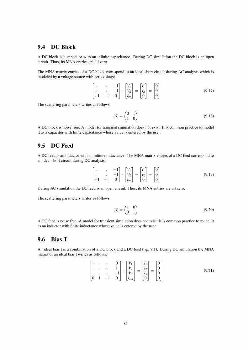
9.4 DC BlockA DC block is a capacitor with an infinite capacitance. During DC simulation the DC block is an opencircuit. Thus, its MNA entries are all zero.
The MNA matrix entries of a DC block correspond to an ideal short circuit during AC analysis which ismodeled by a voltage source with zero voltage. . . +1
. . −1+1 −1 0
·V1
V2Ibr
=
I1I20
=
000
(9.17)
The scattering parameters writes as follows.
(S) =(
0 11 0
)(9.18)
A DC block is noise free. A model for transient simulation does not exist. It is common practice to modelit as a capacitor with finite capacitance whose value is entered by the user.
9.5 DC FeedA DC feed is an inductor with an infinite inductance. The MNA matrix entries of a DC feed correspond toan ideal short circuit during DC analysis: . . +1
. . −1+1 −1 0
·V1
V2Ibr
=
I1I20
=
000
(9.19)
During AC simulation the DC feed is an open circuit. Thus, its MNA entries are all zero.
The scattering parameters writes as follows.
(S) =(
1 00 1
)(9.20)
A DC feed is noise free. A model for transient simulation does not exist. It is common practice to model itas an inductor with finite inductance whose value is entered by the user.
9.6 Bias TAn ideal bias t is a combination of a DC block and a DC feed (fig. 9.1). During DC simulation the MNAmatrix of an ideal bias t writes as follows:
. . . 0
. . . 1
. . . −10 1 −1 0
·
V1V2V3Iout
=
I1I2I30
=
0000
(9.21)
81
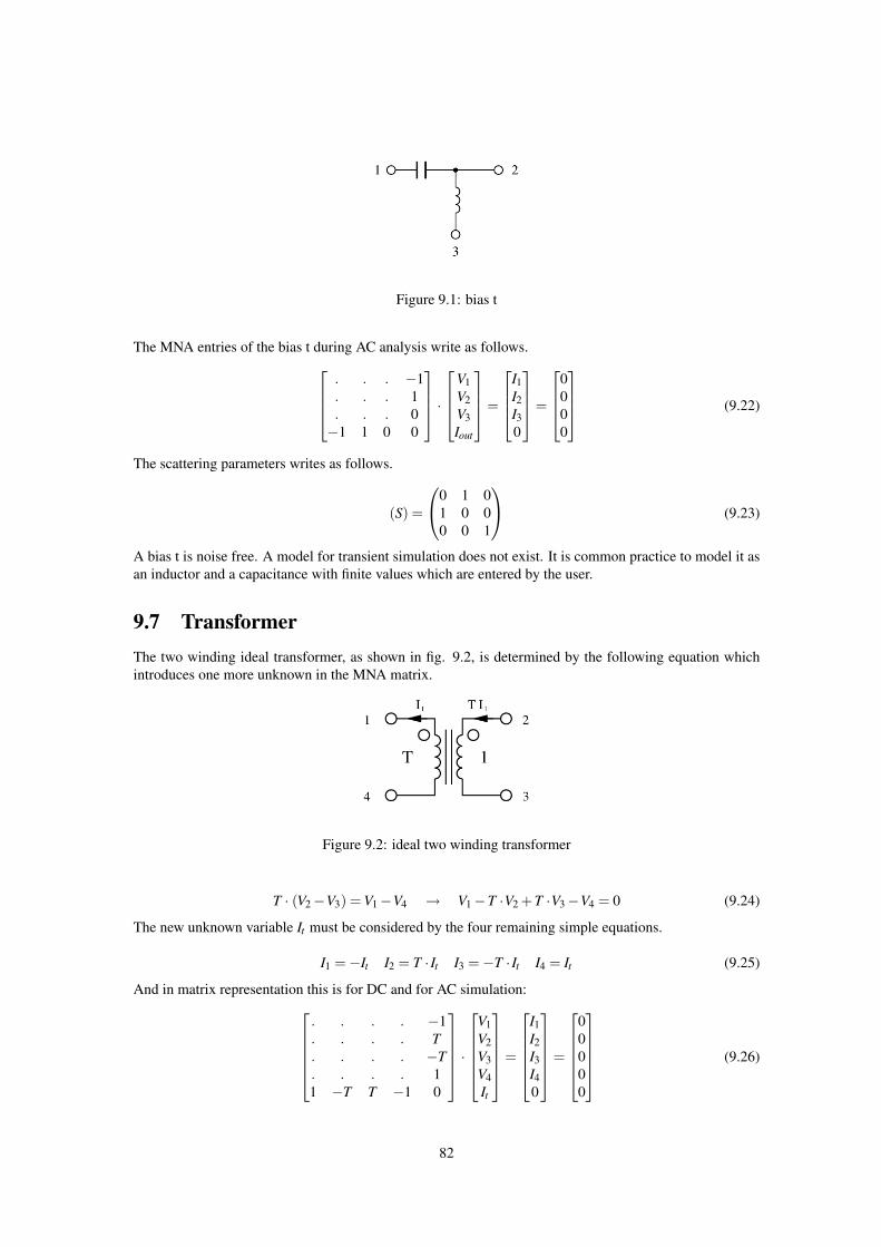
Figure 9.1: bias t
The MNA entries of the bias t during AC analysis write as follows.. . . −1. . . 1. . . 0−1 1 0 0
·
V1V2V3Iout
=
I1I2I30
=
0000
(9.22)
The scattering parameters writes as follows.
(S) =
0 1 01 0 00 0 1
(9.23)
A bias t is noise free. A model for transient simulation does not exist. It is common practice to model it asan inductor and a capacitance with finite values which are entered by the user.
9.7 TransformerThe two winding ideal transformer, as shown in fig. 9.2, is determined by the following equation whichintroduces one more unknown in the MNA matrix.
Figure 9.2: ideal two winding transformer
T · (V2−V3) = V1−V4 → V1−T ·V2 +T ·V3−V4 = 0 (9.24)
The new unknown variable It must be considered by the four remaining simple equations.
I1 =−It I2 = T · It I3 =−T · It I4 = It (9.25)
And in matrix representation this is for DC and for AC simulation:. . . . −1. . . . T. . . . −T. . . . 11 −T T −1 0
·
V1V2V3V4It
=
I1I2I3I40
=
00000
(9.26)
82
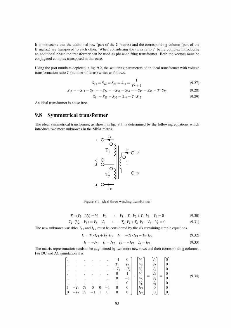
It is noticeable that the additional row (part of the C matrix) and the corresponding column (part of theB matrix) are transposed to each other. When considering the turns ratio T being complex introducingan additional phase the transformer can be used as phase-shifting transformer. Both the vectors must beconjugated complex transposed in this case.
Using the port numbers depicted in fig. 9.2, the scattering parameters of an ideal transformer with voltagetransformation ratio T (number of turns) writes as follows.
S14 = S22 = S33 = S41 =1
T 2 +1(9.27)
S12 =−S13 = S21 =−S24 =−S31 = S34 =−S42 = S43 = T ·S22 (9.28)
S11 = S23 = S32 = S44 = T ·S12 (9.29)
An ideal transformer is noise free.
9.8 Symmetrical transformerThe ideal symmetrical transformer, as shown in fig. 9.3, is determined by the following equations whichintroduce two more unknowns in the MNA matrix.
Figure 9.3: ideal three winding transformer
T1 · (V2−V3) = V1−V6 → V1−T1 ·V2 +T1 ·V3−V6 = 0 (9.30)
T2 · (V2−V3) = V5−V4 → −T2 ·V2 +T2 ·V3−V4 +V5 = 0 (9.31)
The new unknown variables IT 1 and IT 2 must be considered by the six remaining simple equations.
I2 = T1 · IT 1 +T2 · IT 2 I3 =−T1 · IT 1−T2 · IT 2 (9.32)
I1 =−IT 1 I4 = IT 2 I5 =−IT 2 I6 = IT 1 (9.33)
The matrix representation needs to be augmented by two more new rows and their corresponding columns.For DC and AC simulation it is:
. . . . . . −1 0
. . . . . . T1 T2
. . . . . . −T1 −T2
. . . . . . 0 1
. . . . . . 0 −1
. . . . . . 1 01 −T1 T1 0 0 −1 0 00 −T2 T2 −1 1 0 0 0
·
V1V2V3V4V5V6IT 1IT 2
=
I1I2I3I4I5I600
=
00000000
(9.34)
83
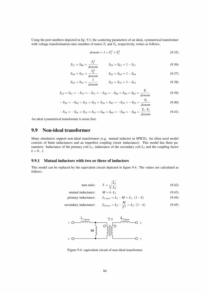
Using the port numbers depicted in fig. 9.3, the scattering parameters of an ideal, symmetrical transformerwith voltage transformation ratio (number of turns) T1 and T2, respectively, writes as follows.
denom = 1+T 21 +T 2
2 (9.35)
S11 = S66 =T 2
1denom
S16 = S61 = 1−S11 (9.36)
S44 = S55 =T 2
2denom
S45 = S54 = 1−S44 (9.37)
S22 = S33 =1
denomS23 = S32 = 1−S22 (9.38)
S12 = S21 =−S13 =−S31 =−S26 =−S62 = S36 = S63 =T1
denom(9.39)
−S24 =−S42 = S25 = S52 = S34 = S43 =−S35 =−S53 =T2
denom(9.40)
−S14 =−S41 = S15 = S51 = S46 = S64 =−S56 =−S65 =T1 ·T2
denom(9.41)
An ideal symmetrical transformer is noise free.
9.9 Non-ideal transformerMany simulators support non-ideal transformers (e.g. mutual inductor in SPICE). An often used modelconsists of finite inductances and an imperfect coupling (straw inductance). This model has three pa-rameters: Inductance of the primary coil L1, inductance of the secondary coil L2 and the coupling factork = 0...1.
9.9.1 Mutual inductors with two or three of inductorsThis model can be replaced by the equivalent circuit depicted in figure 9.4. The values are calculated asfollows.
turn ratio: T =√
L1
L2(9.42)
mutual inductance: M = k ·L1 (9.43)primary inductance: L1,new = L1−M = L1 ·(1− k) (9.44)
secondary inductance: L2,new = L2−MT 2 = L2 ·(1− k) (9.45)
Figure 9.4: equivalent circuit of non-ideal transformer
84
The Y-parameters of this component are:
Y11 = Y44 =−Y41 =−Y14 =1
jω ·L1 ·(1− k2)(9.46)
Y22 = Y33 =−Y23 =−Y32 =1
jω ·L2 ·(1− k2)(9.47)
Y13 = Y31 = Y24 = Y42 =−Y12 =−Y21 =−Y34 =−Y43 =k
jω ·√
L1 ·L2 ·(1− k2)(9.48)
Furthermore, its S-parameters are:
D = (k2−1) · ω2 ·L1 ·L2
2 ·Z0+ jωL1 + jωL2 +2 ·Z0 (9.49)
S14 = S41 =jωL2 +2 ·Z0
D(9.50)
S11 = S44 = 1−S14 (9.51)
S23 = S32 =jωL1 +2 ·Z0
D(9.52)
S22 = S33 = 1−S23 (9.53)
S12 =−S13 = S21 =−S24 =−S31 = S34 =−S42 = S43 =jω ·k ·
√L1 ·L2
D(9.54)
Also including an ohmic resistance R1 and R2 for each coil, leads to the following Y-parameters:
Y11 = Y44 =−Y41 =−Y14 =1
jω ·L1 ·(
1− k2 · jωL2
jωL2 +R2
)+R1
(9.55)
Y22 = Y33 =−Y23 =−Y32 =1
jω ·L2 ·(
1− k2 · jωL1
jωL1 +R1
)+R2
(9.56)
Y13 = Y31 = Y24 = Y42 =−Y12 =−Y21 =−Y34 =−Y43 = k · jω√
L1 ·L2
jω ·L2 +R2·Y11 (9.57)
Building the S-parameters leads to too large equations. Numerically converting the Y-parameters intoS-parameters is therefore recommended.
The MNA matrix entries during DC analysis and the noise correlation matrices of this transformer are:
(Y ) =
1/R1 0 0 −1/R1
0 1/R2 −1/R2 00 −1/R2 1/R2 0
−1/R1 0 0 1/R1
(9.58)
(CY ) = 4 ·k ·T ·
1/R1 0 0 −1/R1
0 1/R2 −1/R2 00 −1/R2 1/R2 0
−1/R1 0 0 1/R1
(9.59)
(CS) = 4 ·k ·T ·Z0 ·
R1
(2·Z0+R1)2 0 0 − R1(2·Z0+R1)2
0 R2(2·Z0+R2)2 − R2
(2·Z0+R2)2 0
0 − R2(2·Z0+R2)2
R2(2·Z0+R2)2 0
− R1(2·Z0+R1)2 0 0 R1
(2·Z0+R1)2
(9.60)
85
A transformer with three coupled inductors has three coupling factors k12, k13 and k23. Its Y-parameterswrite as follows (port numbers are according to figure 9.3).
A = jω ·(1− k212− k2
13− k223 +2 ·k12 ·k13 ·k23) (9.61)
Y11 = Y66 =−Y16 =−Y61 =1− k2
23L1 ·A
(9.62)
Y22 = Y33 =−Y23 =−Y32 =1− k2
12L3 ·A
(9.63)
Y44 = Y55 =−Y45 =−Y54 =1− k2
13L2 ·A
(9.64)
Y12 = Y21 = Y36 = Y63 =−Y13 =−Y31 =−Y26 =−Y62 =k12 ·k23− k13√
L1 ·L3 ·A(9.65)
Y15 = Y51 = Y46 = Y64 =−Y14 =−Y41 =−Y56 =−Y65 =k13 ·k23− k12√
L1 ·L2 ·A(9.66)
Y25 = Y52 = Y43 = Y34 =−Y24 =−Y42 =−Y53 =−Y35 =k12 ·k13− k23√
L2 ·L3 ·A(9.67)
9.9.2 Mutual inductors with any number of inductorsA more general approach for coupled inductors can be obtained by using the induction law:
VL = jωL · IL + jω ·N
∑n=1
kn ·√
L ·Ln · IL,n (9.68)
where VL and IL is the voltage across and the current through the inductor, respectively. L is its inductance.The inductor is coupled with N other inductances Ln. The corresponding coupling factors are kn and IL,nare the currents through the inductors.
Realizing this approach with the MNA matrix is straight forward: Every inductance L needs an additionalmatrix row. The corresponding element in the D matrix is jωL. If two inductors are coupled the crosselement in the D matrix is jωk ·
√L1 ·L2. For two coupled inductors this yields:
. . . . +1 0
. . . . −1 0
. . . . 0 +1
. . . . 0 −1+1 −1 0 0 jωL1 jωk ·
√L1 ·L2
0 0 +1 −1 jωk ·√
L1 ·L2 jωL2
·
V1V2V3V4Ibr1Ibr2
=
I1I2I3I400
=
000000
(9.69)
Obviously, this approach has an advantage: It also works for zero inductances and for unity coupling factorsand is extendible for any number of inductors. It has the disadvantage that it enlarges the MNA matrix.
The S-parameter matrix of this component is obtained by converting the Z-parameter matrix of the compo-nent. The Z-parameter matrix can be constructed using the following scheme: The self-inductances on themain diagonal and the mutual inductances in the off-diagonal entries.
(Z′)
= jω ·[
L1 k ·√
L1 ·L2k ·√
L1 ·L2 L2
](9.70)
This matrix representation does not contain the second terminals of the inductances. That’s why the Z-parameter matrix must be converted into the Y-parameter matrix representation which is then extended to
86
contain the additional terminals.
(Z′)→(Y ′)
=[
y11 y12y21 y22
]→ (Y ) =
+y11 −y11 +y12 −y12−y11 +y11 −y12 +y12+y21 −y21 +y22 −y22−y21 +y21 −y22 +y22
(9.71)
The resulting Y-parameter matrix can be converted into the appropriate S-parameters numerically byeqn. (15.7).
9.10 AttenuatorThe ideal attenuator with (power) attenuation L is frequency independent and the model is valid for DCand for AC simulation. It is determined by the following Z parameters.
Z11 = Z22 = Zre f ·L+1L−1
(9.72)
Z12 = Z21 = Zre f ·2 ·√
LL−1
(9.73)
The Z parameter representation is not very practical as new lines in the MNA matrix have to be added.More useful are the Y parameters.
(Y ) =1
Zre f ·(L−1)·(
L+1 −2 ·√
L−2 ·√
L L+1
)(9.74)
Attenuator with (power) attenuation L, reference impedance Zre f and temperature T :
(CY ) = 4 ·k ·T ·Re(Y ) =4 ·k ·T
Zre f ·(L−1)·(
L+1 −2 ·√
L−2 ·√
L L+1
)(9.75)
The scattering parameters and noise wave correlation matrix of an ideal attenuator with (power) attenuationL (loss) (or power gain G = 1/L) in reference to the impedance Zre f writes as follows.
S11 = S22 =r ·(L−1)
L− r2 =r ·(1−G)1− r2 ·G
(9.76)
S12 = S21 =√
L ·(1− r2)L− r2 =
√G ·(1− r2)1− r2 ·G
(9.77)
(C) = k ·T · (L−1) ·(r2−1)(L− r2)2 ·
(−r2−L 2 ·r
√L
2 ·r√
L −r2−L
)(9.78)
withr =
Zre f −Z0
Zre f +Z0(9.79)
9.11 AmplifierAn ideal amplifier increases signal strength from input to output and blocks all signals flowing into theoutput. The ideal amplifier is an isolator with voltage gain G and is determined by the following Z or Yparameters (valid for DC and AC simulation).
Z11 = Z1 Z12 = 0 (9.80)
Z21 = 2 ·√
Z1 ·Z2 ·G Z22 = Z2 (9.81)
87
Y11 =1Z1
Y12 = 0 (9.82)
Y21 =− 2 ·G√Z1 ·Z2
Y22 =1Z2
(9.83)
With the reference impedance of the input Z1 and the one of the output Z2 and the voltage amplification G,the scattering parameters of an ideal amplifier write as follows.
S11 =Z1−Z0
Z1 +Z0(9.84)
S12 = 0 (9.85)
S22 =Z2−Z0
Z2 +Z0(9.86)
S21 =4 ·Z0 ·
√Z1 ·Z2 ·G
(Z1 +Z0) ·(Z2 +Z0)(9.87)
9.12 IsolatorAn isolator is a one-way two-port, transporting incoming waves lossless from the input (port 1) to the output(port 2), but dissipating all waves flowing into the output. The ideal isolator with reference impedances Z1(input) and Z2 (output) is determined by the following Z parameters (for DC and AC simulation).
Z11 = Z1 Z12 = 0 (9.88)
Z21 = 2 ·√
Z1 ·Z2 Z22 = Z2 (9.89)
A more useful MNA representation is with Y parameters.
(Y ) =
1Z1
0−2√Z1 ·Z2
1Z2
(9.90)
Isolator with reference impedance Z1 (input) and Z2 (output) and temperature T :
(CY ) = 4 ·k ·T ·
1Z1
0−2√Z1 ·Z2
1Z2
(9.91)
With the reference impedance of the input Z1 and the one of the output Z2, the scattering parameters of anideal isolator writes as follows.
S11 =Z1−Z0
Z1 +Z0(9.92)
S12 = 0 (9.93)
S22 =Z2−Z0
Z2 +Z0(9.94)
S21 =√
1− (S11)2 ·√
1− (S22)2 (9.95)
Being on temperature T , the noise wave correlation matrix of an ideal isolator with reference impedanceZ1 and Z2 (input and output) writes as follows.
(C) =4 ·k ·T ·Z0
(Z1 +Z0)2 ·
Z1√
Z1 ·Z2 ·Z0−Z1
Z0 +Z2√
Z1 ·Z2 ·Z0−Z1
Z0 +Z2Z2 ·
(Z1−Z0
Z2 +Z0
)2
(9.96)
88
9.13 CirculatorA circulator is a 3-port device, transporting incoming waves lossless from port 1 to port 2, from port 2 toport 3 and from port 3 to port 1. In all other directions, there is no energy flow. The ideal circulator cannotbe characterized with Z or Y parameters, because their values are partly infinite. But implementing with Sparameters is practical (see equation 9.2).
With the reference impedances Z1, Z2 and Z3 for the ports 1, 2 and 3 the scattering matrix of an idealcirculator writes as follows.
denom = 1− r1 ·r2 ·r3 (9.97)
r1 =Z0−Z1
Z0 +Z1, r2 =
Z0−Z2
Z0 +Z2, r3 =
Z0−Z3
Z0 +Z3(9.98)
S11 =r2 ·r3− r1
denom, S22 =
r1 ·r3− r2
denom, S33 =
r1 ·r2− r3
denom(9.99)
S12 =√
Z2
Z1· Z1 +Z0
Z2 +Z0· r3 ·(1− r2
1)denom
, S13 =√
Z3
Z1· Z1 +Z0
Z3 +Z0· 1− r2
1denom
(9.100)
S21 =√
Z1
Z2· Z2 +Z0
Z1 +Z0· 1− r2
2denom
, S23 =√
Z3
Z2· Z2 +Z0
Z3 +Z0· r1 ·(1− r2
2)denom
(9.101)
S31 =√
Z1
Z3· Z3 +Z0
Z1 +Z0·
r2 ·(1− r23)
denom, S32 =
√Z2
Z3· Z3 +Z0
Z2 +Z0·
1− r23
denom(9.102)
An ideal circulator is noise free.
9.14 Phase shifterA phase shifter alters the phase of the input signal independently on the frequency. As a result the relationbetween input and output signal is complex. To get the DC model, some simulators use the AC formulas andcreate the real part or the magnitude. This procedure has no physical reason, because it uses an operationthat is not defined for DC. But one can think in the following direction: As a DC quantity is constant, itdoesn’t change if it is phase-shifted. (An AC quantity doesn’t change its magnitude, too.) Or to say it withother words, for a DC simulation the phase to shift is always zero. That leads to the result that the phaseshifter is a short circuit for DC. So, this is true for all reference impedances.
For an AC simulation, the Z-parameters of a phase shifter writes as follows.
Z11 = Z22 =j ·Zre f
tan(φ)(9.103)
Z12 = Z21 =j ·Zre f
sin(φ)(9.104)
The admittance parameters required for the AC analysis result in
Y11 = Y22 =j
Zre f · tan(φ)(9.105)
Y12 = Y21 =1
j ·Zre f · sin(φ)(9.106)
where φ denotes the actual phase shift of the device. For a zero phase shift (φ = 0) neither the Z- nor theY-parameters are defined. That is why during AC analysis a phase shifter with zero phase shift representsan ideal short circuit regardless its reference impedance.
89
The MNA matrix entries of an ideal short circuit during AC and DC analysis correspond to a voltage sourcewith zero voltage. The complete MNA matrix representation writes as follows . . +1
. . −1+1 −1 0
·V1
V2Ibr
=
I1I20
=
000
(9.107)
whence Ibr denote the branch current through the voltage source.
The scattering parameters of an ideal phase shifter with phase shift φ and reference impedance Zre f writesas follows.
r =Zre f −Z0
Zre f +Z0(9.108)
S11 = S22 =r · (1− exp( j ·2φ))1− r2 · exp( j ·2φ)
(9.109)
S12 = S21 =(1− r2) · exp( j ·φ)1− r2 · exp( j ·2φ)
(9.110)
An ideal phase shifter is noise free.
9.15 CouplerAccording to the port numbers in fig. 9.5 the Y-parameters of a coupler write as follows.
Y11 = Y22 = Y33 = Y44 =A · (2−A)
D(9.111)
Y12 = Y21 = Y34 = Y43 =−A ·B
D(9.112)
Y13 = Y31 = Y24 = Y42 =C · (A−2)
D(9.113)
Y14 = Y41 = Y23 = Y32 =B ·C
D(9.114)
(9.115)
with
A = k2 · (1+ exp( j ·2φ)) (9.116)
B = 2 ·√
1− k2 (9.117)C = 2 ·k · exp( j ·φ) (9.118)
D = Zre f ·(A2−C2) (9.119)
(9.120)
whereas 0 < k < 1 denotes the coupling factor, φ the phase shift of the coupling path and Zre f the referenceimpedance. The coupler can also be used as hybrid by setting k = 1/
√2. For a 90 degree hybrid, for
example, set φ to π/2. Note that for most couplers no real DC model exists. Taking the real part of the ACmatrix often leads to non-logical results. Thus, it is better to model the coupler for DC by making a shortbetween port 1 and port 2 and between port 3 and port 4. The rest should be an open. This leads to thefollowing MNA matrix.
. . . . 1 0
. . . . −1 0
. . . . 0 1
. . . . 0 −11 −1 0 0 0 00 0 1 −1 0 0
·
V1V2V3V4
Iout1Iout4
=
I1I2I3I400
=
000000
(9.121)
90
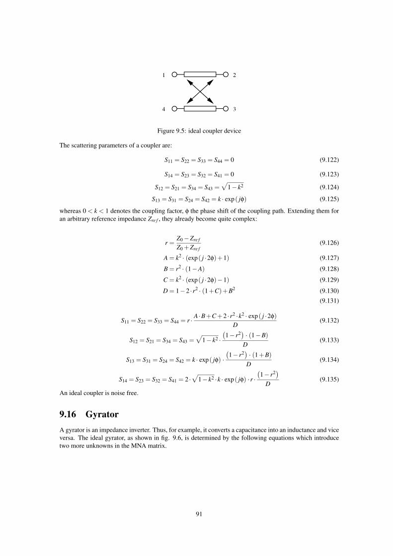
Figure 9.5: ideal coupler device
The scattering parameters of a coupler are:
S11 = S22 = S33 = S44 = 0 (9.122)
S14 = S23 = S32 = S41 = 0 (9.123)
S12 = S21 = S34 = S43 =√
1− k2 (9.124)
S13 = S31 = S24 = S42 = k · exp( jφ) (9.125)
whereas 0 < k < 1 denotes the coupling factor, φ the phase shift of the coupling path. Extending them foran arbitrary reference impedance Zre f , they already become quite complex:
r =Z0−Zre f
Z0 +Zre f(9.126)
A = k2 · (exp( j ·2φ)+1) (9.127)
B = r2 · (1−A) (9.128)
C = k2 · (exp( j ·2φ)−1) (9.129)
D = 1−2 ·r2 · (1+C)+B2 (9.130)(9.131)
S11 = S22 = S33 = S44 = r · A ·B+C +2 ·r2 ·k2 · exp( j ·2φ)D
(9.132)
S12 = S21 = S34 = S43 =√
1− k2 ·(1− r2
)· (1−B)
D(9.133)
S13 = S31 = S24 = S42 = k · exp( jφ) ·(1− r2
)· (1+B)
D(9.134)
S14 = S23 = S32 = S41 = 2 ·√
1− k2 ·k · exp( jφ) ·r ·(1− r2
)D
(9.135)
An ideal coupler is noise free.
9.16 GyratorA gyrator is an impedance inverter. Thus, for example, it converts a capacitance into an inductance and viceversa. The ideal gyrator, as shown in fig. 9.6, is determined by the following equations which introducetwo more unknowns in the MNA matrix.
91
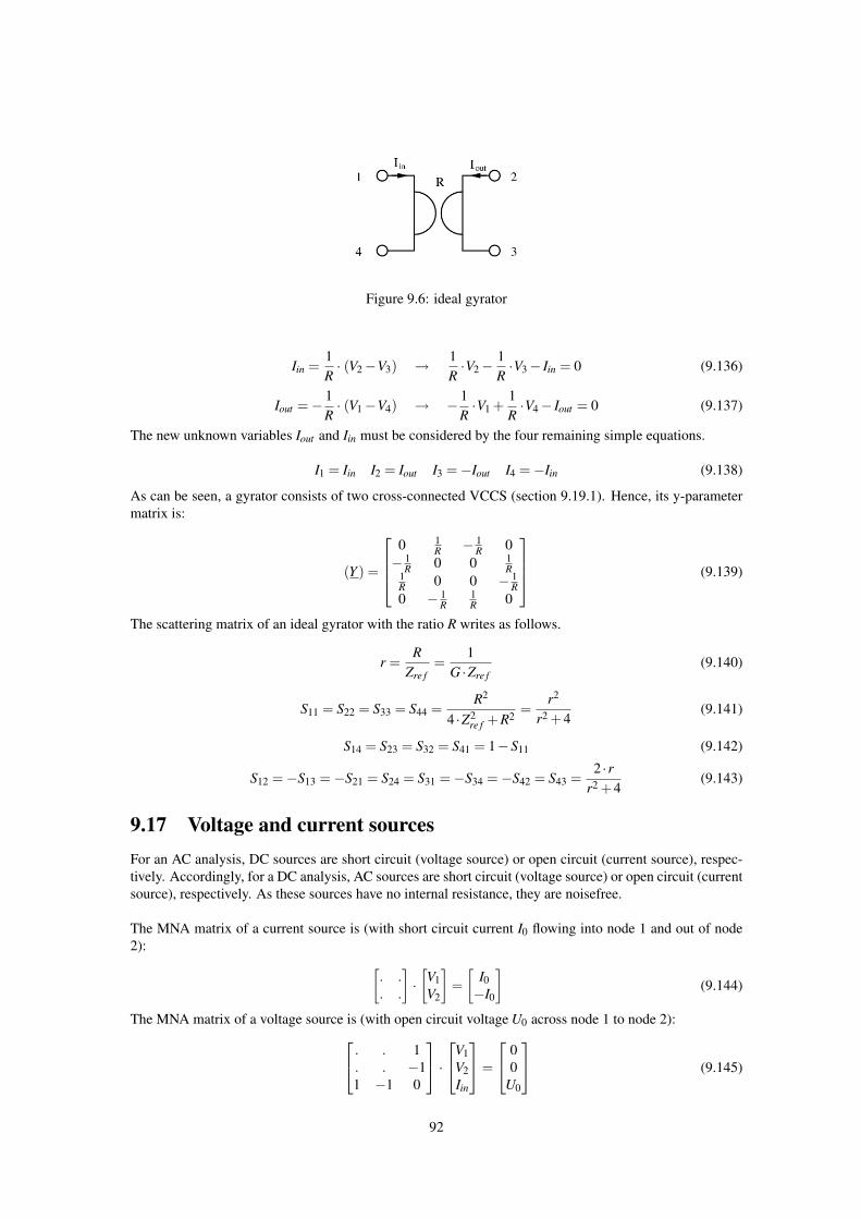
Figure 9.6: ideal gyrator
Iin =1R· (V2−V3) → 1
R·V2−
1R·V3− Iin = 0 (9.136)
Iout =− 1R· (V1−V4) → − 1
R·V1 +
1R·V4− Iout = 0 (9.137)
The new unknown variables Iout and Iin must be considered by the four remaining simple equations.
I1 = Iin I2 = Iout I3 =−Iout I4 =−Iin (9.138)
As can be seen, a gyrator consists of two cross-connected VCCS (section 9.19.1). Hence, its y-parametermatrix is:
(Y ) =
0 1
R − 1R 0
− 1R 0 0 1
R1R 0 0 − 1
R0 − 1
R1R 0
(9.139)
The scattering matrix of an ideal gyrator with the ratio R writes as follows.
r =R
Zre f=
1G ·Zre f
(9.140)
S11 = S22 = S33 = S44 =R2
4 ·Z2re f +R2
=r2
r2 +4(9.141)
S14 = S23 = S32 = S41 = 1−S11 (9.142)
S12 =−S13 =−S21 = S24 = S31 =−S34 =−S42 = S43 =2 ·r
r2 +4(9.143)
9.17 Voltage and current sourcesFor an AC analysis, DC sources are short circuit (voltage source) or open circuit (current source), respec-tively. Accordingly, for a DC analysis, AC sources are short circuit (voltage source) or open circuit (currentsource), respectively. As these sources have no internal resistance, they are noisefree.
The MNA matrix of a current source is (with short circuit current I0 flowing into node 1 and out of node2): [
. .
. .
]·[V1V2
]=[
I0−I0
](9.144)
The MNA matrix of a voltage source is (with open circuit voltage U0 across node 1 to node 2): . . 1. . −11 −1 0
·V1
V2Iin
=
00
U0
(9.145)
92
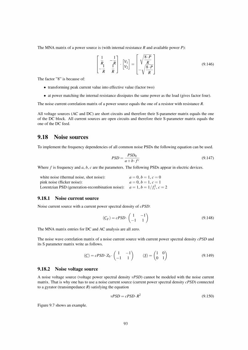
The MNA matrix of a power source is (with internal resistance R and available power P): 1R
− 1R
− 1R
1R
· [V1V2
]=
√
8 ·PR
−√
8 ·PR
(9.146)
The factor ”8” is because of:
• transforming peak current value into effective value (factor two)
• at power matching the internal resistance dissipates the same power as the load (gives factor four).
The noise current correlation matrix of a power source equals the one of a resistor with resistance R.
All voltage sources (AC and DC) are short circuits and therefore their S-parameter matrix equals the oneof the DC block. All current sources are open circuits and therefore their S-parameter matrix equals theone of the DC feed.
9.18 Noise sourcesTo implement the frequency dependencies of all common noise PSDs the following equation can be used.
PSD =PSD0
a+b · f c (9.147)
Where f is frequency and a, b, c are the parameters. The following PSDs appear in electric devices.
white noise (thermal noise, shot noise): a = 0, b = 1, c = 0pink noise (flicker noise): a = 0, b = 1, c = 1Lorentzian PSD (generation-recombination noise): a = 1, b = 1/ f 2
c , c = 2
9.18.1 Noise current sourceNoise current source with a current power spectral density of cPSD:
(CY ) = cPSD ·(
1 −1−1 1
)(9.148)
The MNA matrix entries for DC and AC analysis are all zero.
The noise wave correlation matrix of a noise current source with current power spectral density cPSD andits S parameter matrix write as follows.
(C) = cPSD ·Z0 ·(
1 −1−1 1
)(S) =
(1 00 1
)(9.149)
9.18.2 Noise voltage sourceA noise voltage source (voltage power spectral density vPSD) cannot be modeled with the noise currentmatrix. That is why one has to use a noise current source (current power spectral density cPSD) connectedto a gyrator (transimpedance R) satisfying the equation
vPSD = cPSD ·R2 (9.150)
Figure 9.7 shows an example.
93
Figure 9.7: noise voltage source (left-hand side) and its equivalent circuit (right-hand side)
The MNA matrix entries of the above construct (gyrator ratio R = 1) is similiar to a voltage source withzero voltage. . . −1
. . 11 −1 0
·V1
V2Ix
=
I1I20
=
000
(9.151)
The appropriate noise current correlation matrix yields:
(CY ) = cPSD ·
0 0 00 0 00 0 1
(9.152)
The noise wave correlation matrix of a noise voltage source with voltage power spectral density vPSD andits S parameter matrix write as follows.
(C) =vPSD4 ·Z0
·(
1 −1−1 1
)(S) =
(0 11 0
)(9.153)
9.18.3 Correlated noise sourcesFor two correlated noise current sources the (normalized) correlation coefficient K must be known (with|K| = 0 . . .1). If the first noise source has the current power spectral density Si1 and is connected to node1 and 2, and if furthermore the second noise source has the spectral density Si2 and is connected to node 3and 4, then the correlation matrix writes:
(CY ) =
Si1 −Si1 K ·
√Si1 ·Si2 −K ·
√Si1 ·Si2
−Si1 Si1 −K ·√
Si1 ·Si2 K ·√
Si1 ·Si2K ·√
Si1 ·Si2 −K ·√
Si1 ·Si2 Si2 −Si2−K ·√
Si1 ·Si2 K ·√
Si1 ·Si2 −Si2 Si2
(9.154)
The MNA matrix entries for DC and AC analysis are all zero.
The noise wave correlation matrix of two correlated noise current sources with current power spectraldensities Si1 and Si2 and correlation coefficient K writes as follows.
(C) = Z0 ·
Si1 −Si1 K ·
√Si1 ·Si2 −K ·
√Si1 ·Si2
−Si1 Si1 −K ·√
Si1 ·Si2 K ·√
Si1 ·Si2K ·√
Si1 ·Si2 −K ·√
Si1 ·Si2 Si2 −Si2−K ·√
Si1 ·Si2 K ·√
Si1 ·Si2 −Si2 Si2
(9.155)
(S) =
1 0 0 00 1 0 00 0 1 00 0 0 1
(9.156)
For two correlated noise voltage sources two extra rows and columns are needed in the MNA matrix:
94
. . . . −1 0. . . . 1 0. . . . 0 −1. . . . 0 11 −1 0 0 0 00 0 1 −1 0 0
·
V1V2V3V4Ix1Ix2
=
I1I2I3I400
=
000000
(9.157)
The appropriate noise current correlation matrix (with the noise voltage power spectral densities Sv1 andSv2 and the correlation coefficient K) yields:
(CY ) =
0 0 0 0 0 00 0 0 0 0 00 0 0 0 0 00 0 0 0 0 00 0 0 0 Sv1 K ·
√Sv1 ·Sv2
0 0 0 0 K ·√
Sv1 ·Sv2 Sv2
(9.158)
The noise wave correlation matrix of two correlated noise voltage sources with voltage power spectraldensities Sv1 and Sv2 and correlation coefficient K and its S parameter matrix write as follows.
(C) =1
4 ·Z0·
Sv1 −Sv1 K ·
√Sv1 ·Sv2 −K ·
√Sv1 ·Sv2
−Sv1 Sv1 −K ·√
Sv1 ·Sv2 K ·√
Sv1 ·Sv2K ·√
Sv1 ·Sv2 −K ·√
Sv1 ·Sv2 Sv2 −Sv2−K ·√
Sv1 ·Sv2 K ·√
Sv1 ·Sv2 −Sv2 Sv2
(9.159)
(S) =
0 1 0 01 0 0 00 0 0 10 0 1 0
(9.160)
If a noise current source (ports 1 and 2) and a noise voltage source (ports 3 and 4) are correlated, the MNAmatrix entries are as follows.
. . . . 0
. . . . 0
. . . . −1
. . . . 10 0 1 −1 0
·
V1V2V3V4Ix
=
I1I2I3I40
=
00000
(9.161)
The appropriate noise current correlation matrix (with the noise power spectral densities Si1 and Sv2 andthe correlation coefficient K) yields:
(CY ) =
Si1 −Si1 0 0 K ·
√Si1 ·Sv2
−Si1 Si1 0 0 00 0 0 0 00 0 0 0 0
K ·√
Si1 ·Sv2 0 0 0 Sv2
(9.162)
Note: Because the gyrator factor (It is unity.) has been omitted in the above matrix the units are not correct.This can be ignored.
The noise wave correlation matrix of one correlated noise current source Si1 and one noise voltage sourceSv2 with correlation coefficient K writes as follows.
(C) =
Z0 ·Si1 −Z0 ·Si1 K/2 ·
√Si1 ·Sv2 −K/2 ·
√Si1 ·Sv2
−Z0 ·Si1 Z0 ·Si1 −K/2 ·√
Si1 ·Sv2 K/2 ·√
Si1 ·Sv2K/2 ·
√Si1 ·Sv2 −K/2 ·
√Si1 ·Sv2 Sv2/4/Z0 −Sv2/4/Z0
−K/2 ·√
Si1 ·Sv2 K/2 ·√
Si1 ·Sv2 −Sv2/4/Z0 Sv2/4/Z0
(9.163)
95
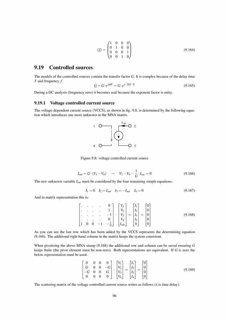
(S) =
1 0 0 00 1 0 00 0 0 10 0 1 0
(9.164)
9.19 Controlled sourcesThe models of the controlled sources contain the transfer factor G. It is complex because of the delay timeT and frequency f .
G = G ·e jωT = G ·e j ·2π f ·T (9.165)
During a DC analysis (frequency zero) it becomes real because the exponent factor is unity.
9.19.1 Voltage controlled current sourceThe voltage-dependent current source (VCCS), as shown in fig. 9.8, is determined by the following equa-tion which introduces one more unknown in the MNA matrix.
Figure 9.8: voltage controlled current source
Iout = G · (V1−V4) → V1−V4−1G· Iout = 0 (9.166)
The new unknown variable Iout must be considered by the four remaining simple equations.
I1 = 0 I2 = Iout I3 =−Iout I4 = 0 (9.167)
And in matrix representation this is:. . . . 0. . . . 1. . . . −1. . . . 01 0 0 −1 − 1
G
·
V1V2V3V4Iout
=
I1I2I3I40
=
00000
(9.168)
As you can see the last row which has been added by the VCCS represents the determining equation(9.166). The additional right hand column in the matrix keeps the system consistent.
When pivotising the above MNA stamp (9.168) the additional row and column can be saved ensuring Gkeeps finite (the pivot element must be non-zero). Both representations are equivalent. If G is zero thebelow representation must be used.
0 0 0 0G 0 0 −G−G 0 0 G0 0 0 0
·
V1V2V3V4
=
I1I2I3I4
=
0000
(9.169)
The scattering matrix of the voltage controlled current source writes as follows (τ is time delay).
96
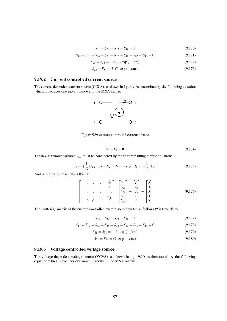
S11 = S22 = S33 = S44 = 1 (9.170)
S12 = S13 = S14 = S23 = S32 = S41 = S42 = S43 = 0 (9.171)
S21 = S34 =−2 ·G · exp(− jωτ) (9.172)
S24 = S31 = 2 ·G · exp(− jωτ) (9.173)
9.19.2 Current controlled current sourceThe current-dependent current source (CCCS), as shown in fig. 9.9, is determined by the following equationwhich introduces one more unknown in the MNA matrix.
Figure 9.9: current controlled current source
V1−V4 = 0 (9.174)
The new unknown variable Iout must be considered by the four remaining simple equations.
I1 = +1G· Iout I2 = Iout I3 =−Iout I4 =− 1
G· Iout (9.175)
And in matrix representation this is:. . . . 1
G. . . . 1. . . . −1. . . . − 1
G1 0 0 −1 0
·
V1V2V3V4Iout
=
I1I2I3I40
=
00000
(9.176)
The scattering matrix of the current controlled current source writes as follows (τ is time delay).
S14 = S22 = S33 = S41 = 1 (9.177)
S11 = S12 = S13 = S23 = S32 = S42 = S43 = S44 = 0 (9.178)
S21 = S34 =−G · exp(− jωτ) (9.179)
S24 = S31 = G · exp(− jωτ) (9.180)
9.19.3 Voltage controlled voltage sourceThe voltage-dependent voltage source (VCVS), as shown in fig. 9.10, is determined by the followingequation which introduces one more unknown in the MNA matrix.
97
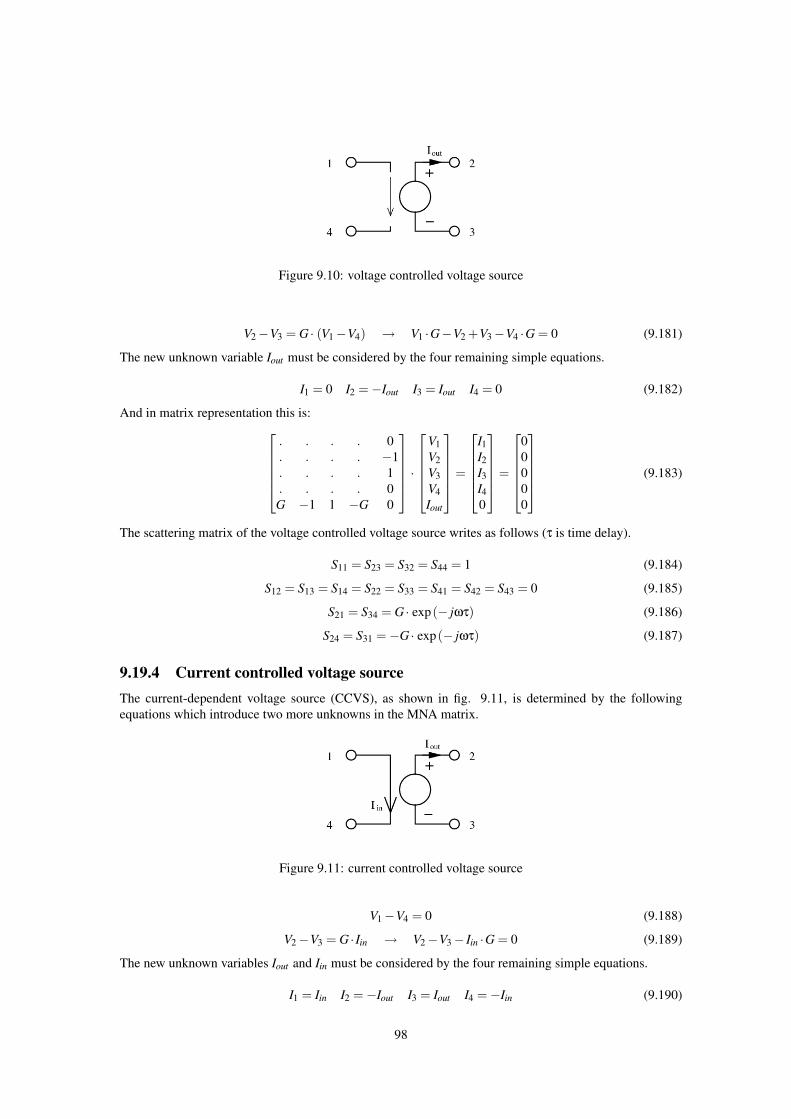
Figure 9.10: voltage controlled voltage source
V2−V3 = G · (V1−V4) → V1 ·G−V2 +V3−V4 ·G = 0 (9.181)
The new unknown variable Iout must be considered by the four remaining simple equations.
I1 = 0 I2 =−Iout I3 = Iout I4 = 0 (9.182)
And in matrix representation this is:. . . . 0. . . . −1. . . . 1. . . . 0G −1 1 −G 0
·
V1V2V3V4Iout
=
I1I2I3I40
=
00000
(9.183)
The scattering matrix of the voltage controlled voltage source writes as follows (τ is time delay).
S11 = S23 = S32 = S44 = 1 (9.184)
S12 = S13 = S14 = S22 = S33 = S41 = S42 = S43 = 0 (9.185)
S21 = S34 = G · exp(− jωτ) (9.186)
S24 = S31 =−G · exp(− jωτ) (9.187)
9.19.4 Current controlled voltage sourceThe current-dependent voltage source (CCVS), as shown in fig. 9.11, is determined by the followingequations which introduce two more unknowns in the MNA matrix.
Figure 9.11: current controlled voltage source
V1−V4 = 0 (9.188)
V2−V3 = G · Iin → V2−V3− Iin ·G = 0 (9.189)
The new unknown variables Iout and Iin must be considered by the four remaining simple equations.
I1 = Iin I2 =−Iout I3 = Iout I4 =−Iin (9.190)
98
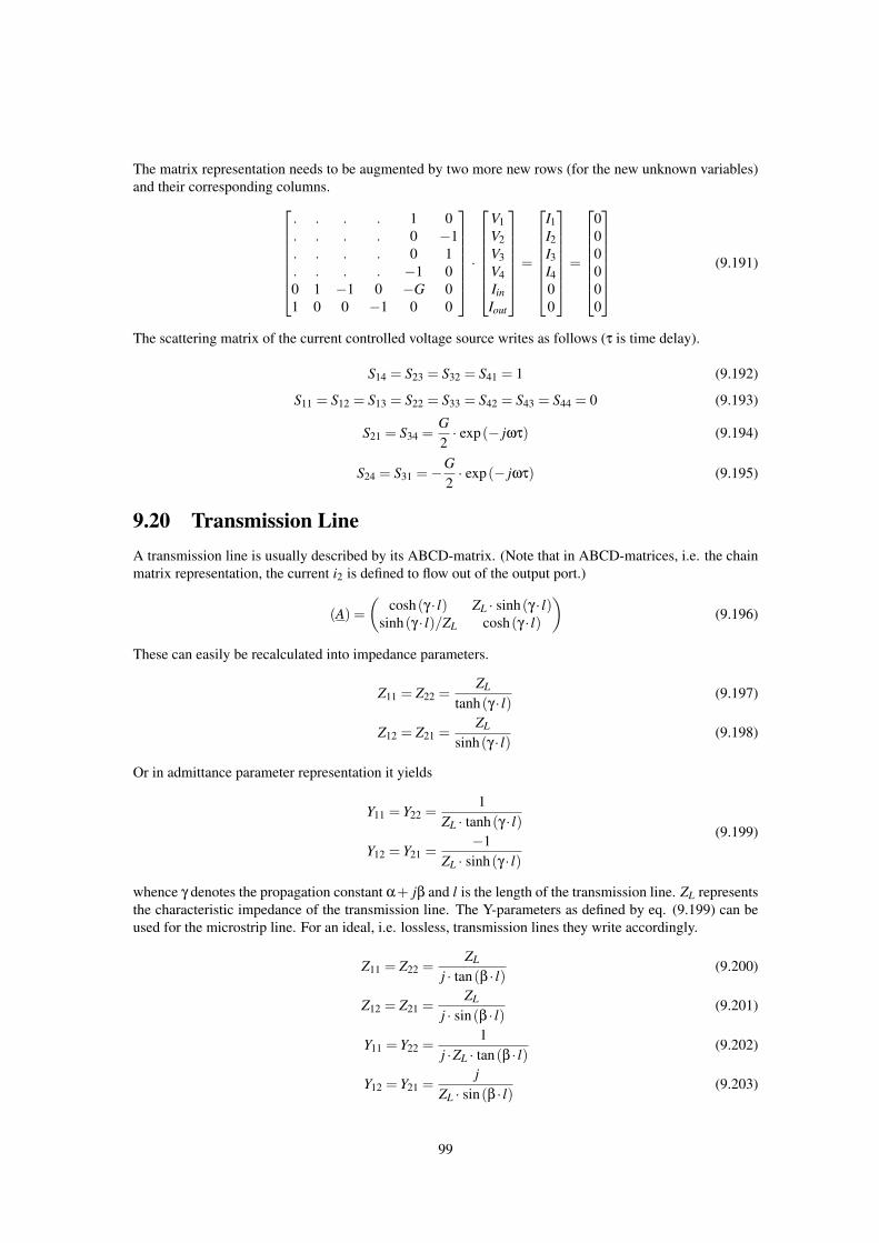
The matrix representation needs to be augmented by two more new rows (for the new unknown variables)and their corresponding columns.
. . . . 1 0
. . . . 0 −1
. . . . 0 1
. . . . −1 00 1 −1 0 −G 01 0 0 −1 0 0
·
V1V2V3V4IinIout
=
I1I2I3I400
=
000000
(9.191)
The scattering matrix of the current controlled voltage source writes as follows (τ is time delay).
S14 = S23 = S32 = S41 = 1 (9.192)
S11 = S12 = S13 = S22 = S33 = S42 = S43 = S44 = 0 (9.193)
S21 = S34 =G2· exp(− jωτ) (9.194)
S24 = S31 =−G2· exp(− jωτ) (9.195)
9.20 Transmission LineA transmission line is usually described by its ABCD-matrix. (Note that in ABCD-matrices, i.e. the chainmatrix representation, the current i2 is defined to flow out of the output port.)
(A) =(
cosh(γ · l) ZL · sinh(γ · l)sinh(γ · l)/ZL cosh(γ · l)
)(9.196)
These can easily be recalculated into impedance parameters.
Z11 = Z22 =ZL
tanh(γ · l)(9.197)
Z12 = Z21 =ZL
sinh(γ · l)(9.198)
Or in admittance parameter representation it yields
Y11 = Y22 =1
ZL · tanh(γ · l)
Y12 = Y21 =−1
ZL · sinh(γ · l)
(9.199)
whence γ denotes the propagation constant α+ jβ and l is the length of the transmission line. ZL representsthe characteristic impedance of the transmission line. The Y-parameters as defined by eq. (9.199) can beused for the microstrip line. For an ideal, i.e. lossless, transmission lines they write accordingly.
Z11 = Z22 =ZL
j · tan(β · l)(9.200)
Z12 = Z21 =ZL
j · sin(β · l)(9.201)
Y11 = Y22 =1
j ·ZL · tan(β · l)(9.202)
Y12 = Y21 =j
ZL · sin(β · l)(9.203)
99
The scattering matrix of an ideal, lossless transmission line with impedance Z and electrical length l writesas follows.
r =Z−Z0
Z +Z0(9.204)
p = exp(− jω
lc0
)(9.205)
S11 = S22 =r ·(1− p2)1− r2 · p2 , S12 = S21 =
p ·(1− r2)1− r2 · p2 (9.206)
With c0 = 299 792 458 m/s being the vacuum light velocity. Adding attenuation to the transmission line,the quantity p extends to:
p = exp(− jω
lc0−α · l
)(9.207)
Another equivalent equation set for the calculation of the scattering parameters is the following: With thephysical length l of the component, its impedance ZL and propagation constant γ, the complex propagationconstant γ is given by
γ = α+ jβ (9.208)
where α is the attenuation factor and β is the (real) propagation constant given by
β =√
εre f f (ω) ·k0 (9.209)
where εre f f (ω) is the effective dielectric constant and k0 is the TEM propagation constant k0 for the equiv-alent transmission line with an air dielectric.
k0 = ω√
ε0µ0 (9.210)
The expressions used to calculate the scattering parameters are given by
S11 = S22 =(z− y)sinhγl
2coshγl +(z+ y)sinhγl(9.211)
S12 = S21 =2
2coshγl +(z+ y)sinhγl(9.212)
with z being the normalized impedance and y is the normalized admittance.
9.21 Differential Transmission LineA differential (4-port) transmission line is not referenced to ground potential, i.e. the wave from the input(port 1 and 4) is distributed to the output (port 2 and 3). Its admittance parameters are:
Y11 = Y22 = Y33 = Y44 =−Y14 =−Y41 =−Y23 =−Y32 =1
ZL · tanh(γ · l)(9.213)
Y13 = Y31 = Y24 = Y42 =−Y12 =−Y21 =−Y34 =−Y43 =1
ZL · sinh(γ · l)(9.214)
The scattering parameters writes:
S11 = S22 = S33 = S44 = ZL ·(2 ·Z0 +ZL) · exp(2 ·γ · l)+(2 ·Z0−ZL)
(2 ·Z0 +ZL)2 · exp(2 ·γ · l)− (2 ·Z0−ZL)2 (9.215)
S14 = S41 = S23 = S32 = 1−S11 (9.216)
100
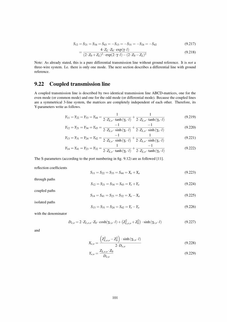
S12 = S21 = S34 = S43 =−S13 =−S31 =−S24 =−S42 (9.217)
=4 ·ZL ·Z0 · exp(γ · l)
(2 ·Z0 +ZL)2 · exp(2 ·γ · l)− (2 ·Z0−ZL)2 (9.218)
Note: As already stated, this is a pure differential transmission line without ground reference. It is not athree-wire system. I.e. there is only one mode. The next section describes a differential line with groundreference.
9.22 Coupled transmission lineA coupled transmission line is described by two identical transmission line ABCD-matrices, one for theeven mode (or common mode) and one for the odd mode (or differential mode). Because the coupled linesare a symmetrical 3-line system, the matrices are completely independent of each other. Therefore, itsY-parameters write as follows.
Y11 = Y22 = Y33 = Y44 =1
2 ·ZL,e · tanh(γe · l)+
12 ·ZL,o · tanh(γo · l)
(9.219)
Y12 = Y21 = Y34 = Y43 =−1
2 ·ZL,e · sinh(γe · l)+
−12 ·ZL,o · sinh(γo · l)
(9.220)
Y13 = Y31 = Y24 = Y42 =−1
2 ·ZL,e · sinh(γe · l)+
12 ·ZL,o · sinh(γo · l)
(9.221)
Y14 = Y41 = Y23 = Y32 =1
2 ·ZL,e · tanh(γe · l)+
−12 ·ZL,o · tanh(γo · l)
(9.222)
The S-parameters (according to the port numbering in fig. 9.12) are as followed [11].
reflection coefficientsS11 = S22 = S33 = S44 = Xe +Xo (9.223)
through pathsS12 = S21 = S34 = S43 = Ye +Yo (9.224)
coupled pathsS14 = S41 = S23 = S32 = Xe−Xo (9.225)
isolated pathsS13 = S31 = S24 = S42 = Ye−Yo (9.226)
with the denominator
De,o = 2 ·ZL,e,o ·Z0 · cosh(γe,o · l)+(Z2
L,e,o +Z20)· sinh(γe,o · l) (9.227)
and
Xe,o =
(Z2
L,e,o−Z20
)· sinh(γe,o · l)
2 ·De,o(9.228)
Ye,o =ZL,e,o ·Z0
De,o(9.229)
101
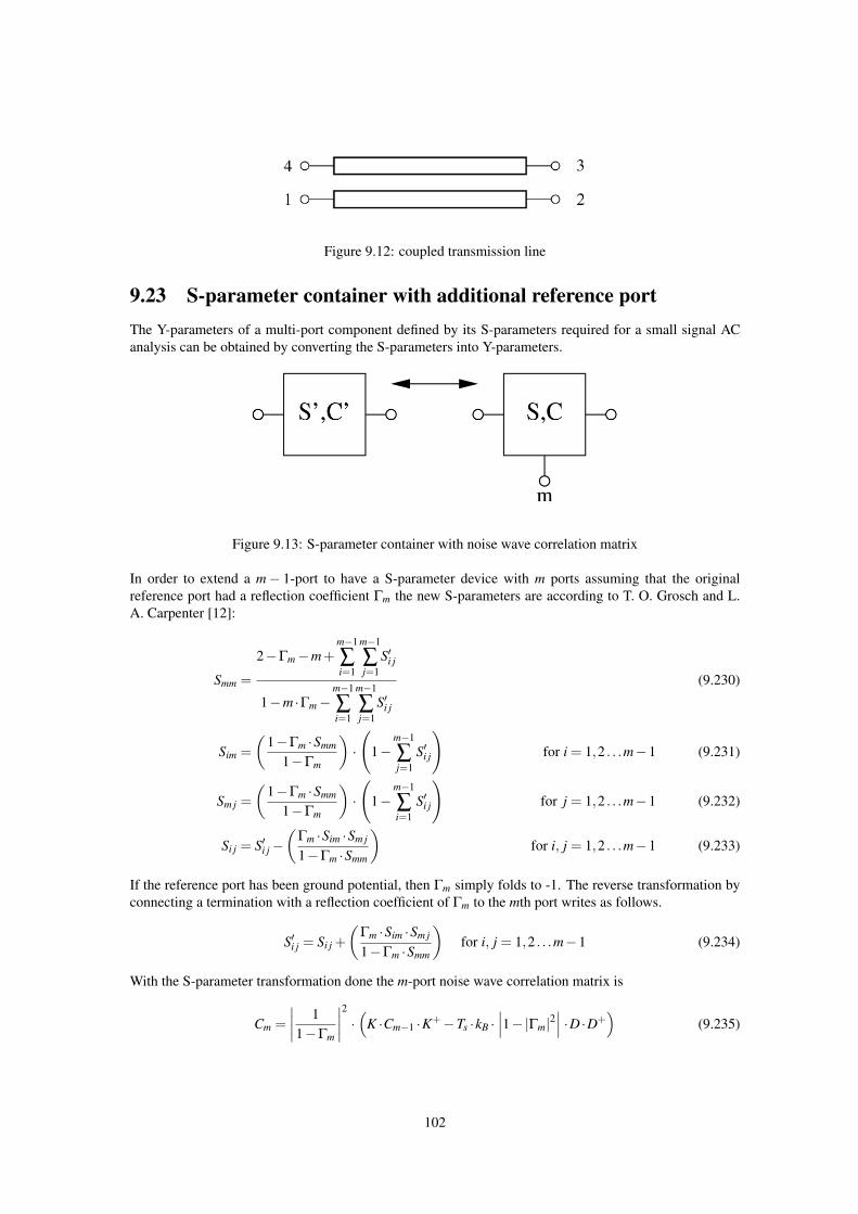
Figure 9.12: coupled transmission line
9.23 S-parameter container with additional reference portThe Y-parameters of a multi-port component defined by its S-parameters required for a small signal ACanalysis can be obtained by converting the S-parameters into Y-parameters.
Figure 9.13: S-parameter container with noise wave correlation matrix
In order to extend a m− 1-port to have a S-parameter device with m ports assuming that the originalreference port had a reflection coefficient Γm the new S-parameters are according to T. O. Grosch and L.A. Carpenter [12]:
Smm =
2−Γm−m+m−1
∑i=1
m−1
∑j=1
S′i j
1−m ·Γm−m−1
∑i=1
m−1
∑j=1
S′i j
(9.230)
Sim =(
1−Γm ·Smm
1−Γm
)·
(1−
m−1
∑j=1
S′i j
)for i = 1,2 . . .m−1 (9.231)
Sm j =(
1−Γm ·Smm
1−Γm
)·
(1−
m−1
∑i=1
S′i j
)for j = 1,2 . . .m−1 (9.232)
Si j = S′i j−(
Γm ·Sim ·Sm j
1−Γm ·Smm
)for i, j = 1,2 . . .m−1 (9.233)
If the reference port has been ground potential, then Γm simply folds to -1. The reverse transformation byconnecting a termination with a reflection coefficient of Γm to the mth port writes as follows.
S′i j = Si j +(
Γm ·Sim ·Sm j
1−Γm ·Smm
)for i, j = 1,2 . . .m−1 (9.234)
With the S-parameter transformation done the m-port noise wave correlation matrix is
Cm =∣∣∣∣ 11−Γm
∣∣∣∣2 · (K ·Cm−1 ·K+−Ts ·kB ·∣∣∣1−|Γm|2
∣∣∣ ·D ·D+)
(9.235)
102
with
K =
1+Γm (S1m−1) ΓmS1m . . . ΓmS1m
ΓmS2m 1+Γm (S2m−1) . . . ΓmS2m...
.... . .
...ΓmS(m−1)m ΓmS(m−1)m . . . 1+Γm
(S(m−1)m−1
)ΓmSmm−1 ΓmSmm−1 . . . ΓmSmm−1
(9.236)
D =
S1mS2m
...S(m−1)mSmm−1
(9.237)
whence Ts denotes the equivalent noise temperature of the original reference port and the + operator indi-cates the transposed conjugate matrix (also called adjoint or adjugate).
The reverse transformation can be written as
Cm−1 = K′ ·Cm ·K′+ +Ts ·kB ·
∣∣∣1−|Γm|2∣∣∣
|1−ΓmSmm|2·D′ ·D′+ (9.238)
with
K′ =
1 0 . . . 0ΓmS1m
1−ΓmSmm
0 1 . . . 0ΓmS2m
1−ΓmSmm
. .. . . .
...
0 0 . . . 1ΓmS(m−1)m
1−ΓmSmm
(9.239)
D′ =
S1mS2m
...S(m−1)m
(9.240)
9.24 Real-Life ModelsNon-ideal electronic components exhibit parasitic effects. Depending on the usage, they may show avery different behaviour than the ideal ones. More precise models can sometimes be obtained from theirmanufacturers or vendors. However, first oder approximations exists that can give satisfactory result inmany cases. A few of these simple models are presented in this chapter.
103
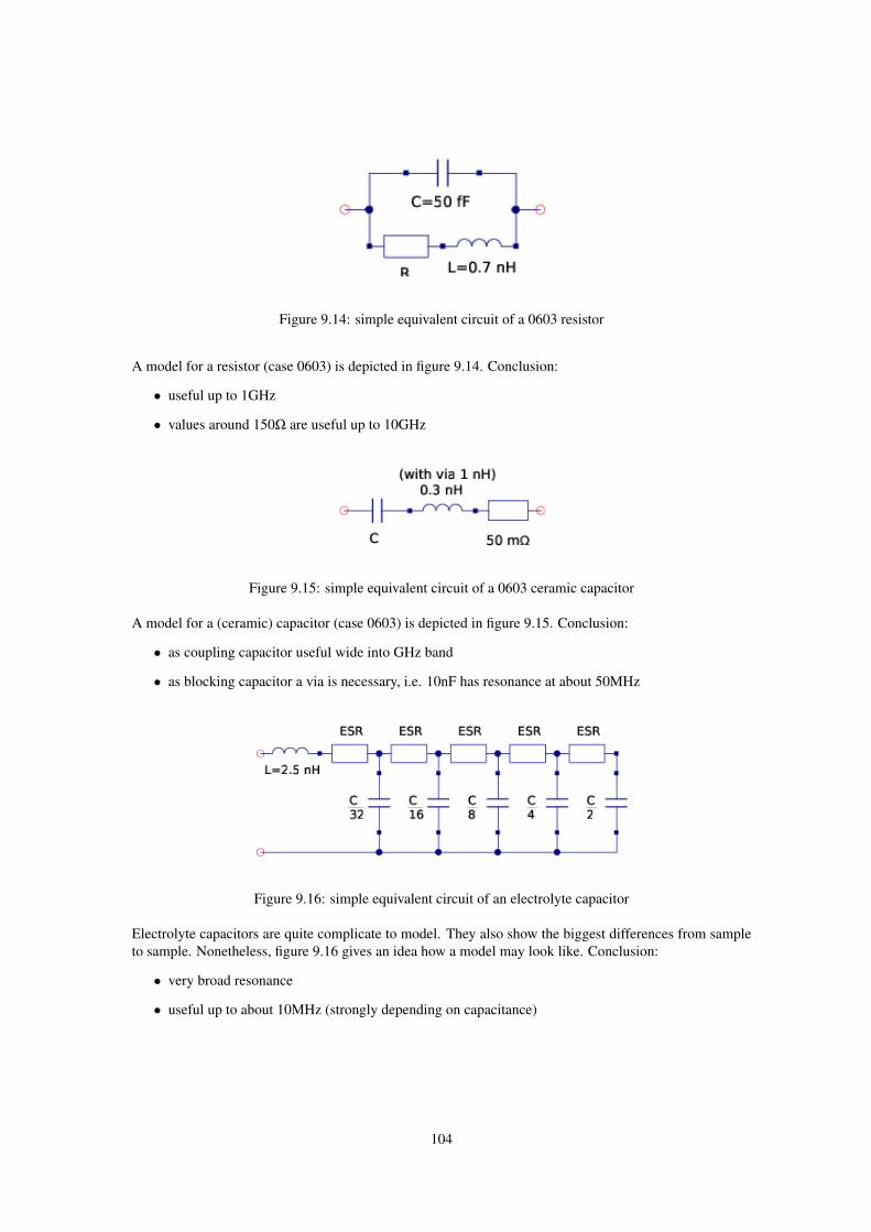
Figure 9.14: simple equivalent circuit of a 0603 resistor
A model for a resistor (case 0603) is depicted in figure 9.14. Conclusion:
• useful up to 1GHz
• values around 150Ω are useful up to 10GHz
Figure 9.15: simple equivalent circuit of a 0603 ceramic capacitor
A model for a (ceramic) capacitor (case 0603) is depicted in figure 9.15. Conclusion:
• as coupling capacitor useful wide into GHz band
• as blocking capacitor a via is necessary, i.e. 10nF has resonance at about 50MHz
Figure 9.16: simple equivalent circuit of an electrolyte capacitor
Electrolyte capacitors are quite complicate to model. They also show the biggest differences from sampleto sample. Nonetheless, figure 9.16 gives an idea how a model may look like. Conclusion:
• very broad resonance
• useful up to about 10MHz (strongly depending on capacitance)
104
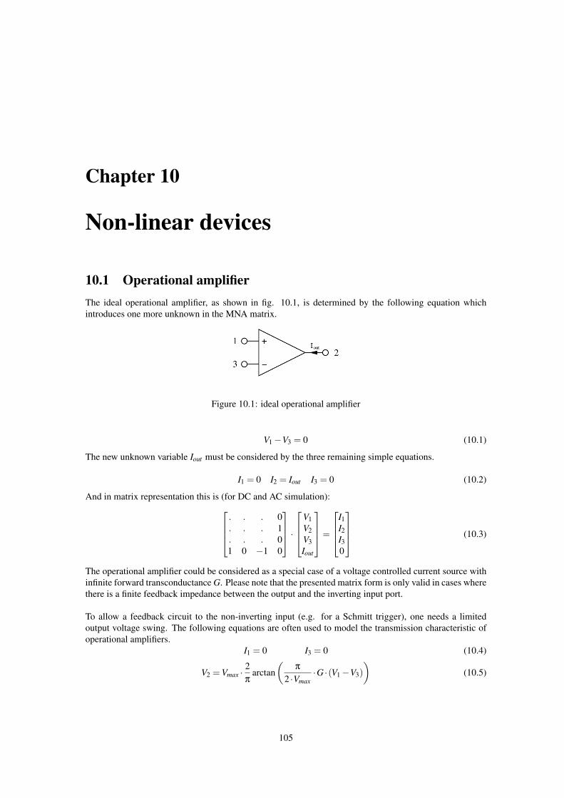
Chapter 10
Non-linear devices
10.1 Operational amplifierThe ideal operational amplifier, as shown in fig. 10.1, is determined by the following equation whichintroduces one more unknown in the MNA matrix.
Figure 10.1: ideal operational amplifier
V1−V3 = 0 (10.1)
The new unknown variable Iout must be considered by the three remaining simple equations.
I1 = 0 I2 = Iout I3 = 0 (10.2)
And in matrix representation this is (for DC and AC simulation):. . . 0. . . 1. . . 01 0 −1 0
·
V1V2V3Iout
=
I1I2I30
(10.3)
The operational amplifier could be considered as a special case of a voltage controlled current source withinfinite forward transconductance G. Please note that the presented matrix form is only valid in cases wherethere is a finite feedback impedance between the output and the inverting input port.
To allow a feedback circuit to the non-inverting input (e.g. for a Schmitt trigger), one needs a limitedoutput voltage swing. The following equations are often used to model the transmission characteristic ofoperational amplifiers.
I1 = 0 I3 = 0 (10.4)
V2 = Vmax ·2π
arctan(
π
2 ·Vmax·G ·(V1−V3)
)(10.5)
105
with Vmax being the maximum output voltage swing and G the voltage amplification. To model the small-signal behaviour (AC analysis), it is necessary to differentiate:
g =∂V2
∂(V1−V3)=
G
1+(
π
2 ·Vmax·G ·(V1−V3)
)2 (10.6)
This leads to the following matrix representation being a specialised three node voltage controlled voltagesource (see section 9.19.3 on page 97).
. . . 0
. . . 1
. . . 0g −1 −g 0
·
V1V2V3Iout
=
I1I2I30
(10.7)
The above MNA matrix entries are also used during the non-linear DC analysis with the 0 in the right handside vector replaced by an equivalent voltage
Veq = g · (V1−V3)−Vout (10.8)
with Vout computed using eq. (10.5).
With the given small-signal matrix representation, building the S-parameters is easy.
(S) =
1 0 04g −1 −4g0 0 1
(10.9)
10.2 PN-Junction DiodeThe following table contains the model parameters for the pn-junction diode model.
Name Symbol Description Unit DefaultIs IS saturation current A 10−14
N N emission coefficient 1.0Isr ISR recombination current parameter A 0.0Nr NR emission coefficient for Isr 2.0Rs RS ohmic resistance Ω 0.0
Cj0 C j0 zero-bias junction capacitance F 0.0M M grading coefficient 0.5Vj Vj junction potential V 0.7Fc Fc forward-bias depletion capacitance coefficient 0.5Cp Cp linear capacitance F 0.0Tt τ transit time s 0.0
Bv Bv reverse breakdown voltage V ∞
Ibv IBv current at reverse breakdown voltage A 0.001Kf KF flicker noise coefficient 0.0Af AF flicker noise exponent 1.0
Ffe FFE flicker noise frequency exponent 1.0Temp T device temperature C 26.85
Xti XT I saturation current exponent 3.0Eg EG energy bandgap eV 1.11
Tbv TBv Bv linear temperature coefficient 1/C 0.0Trs TRS Rs linear temperature coefficient 1/C 0.0
106
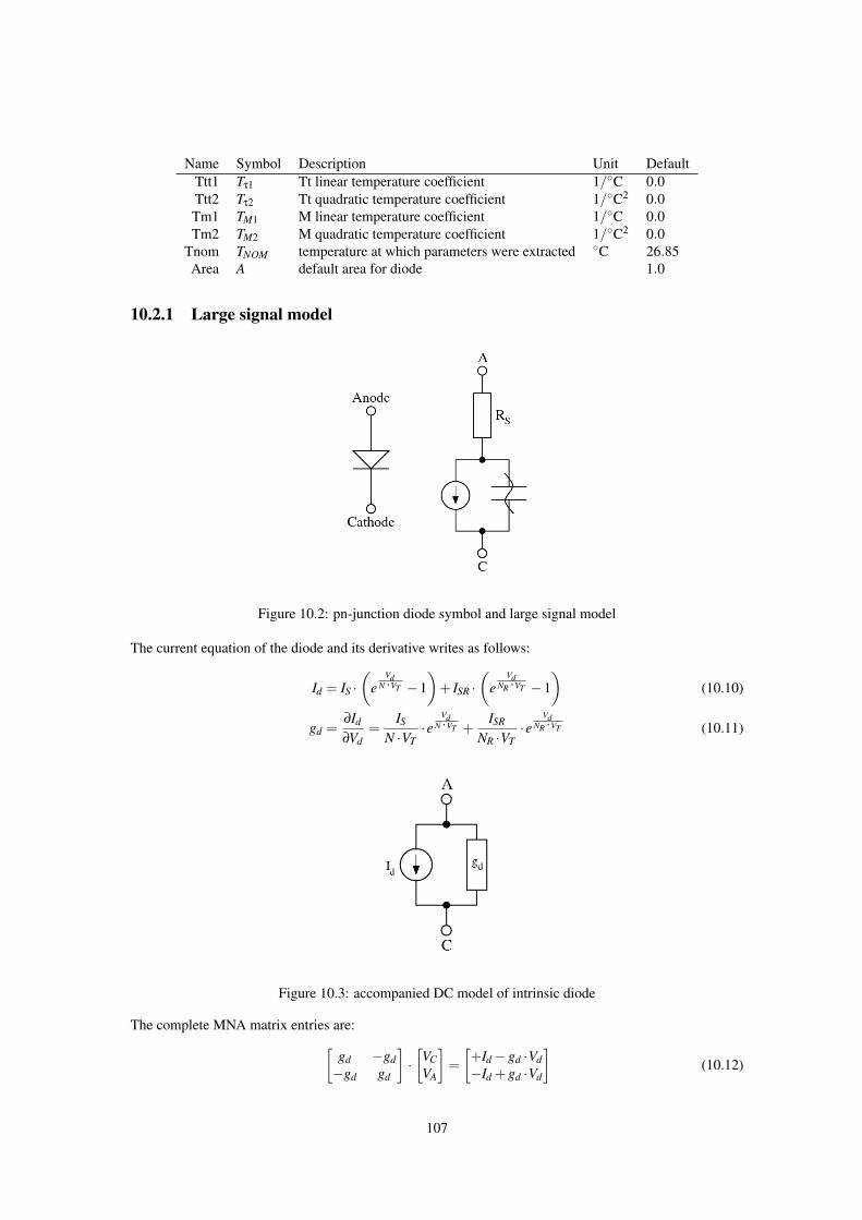
Name Symbol Description Unit DefaultTtt1 Tτ1 Tt linear temperature coefficient 1/C 0.0Ttt2 Tτ2 Tt quadratic temperature coefficient 1/C2 0.0Tm1 TM1 M linear temperature coefficient 1/C 0.0Tm2 TM2 M quadratic temperature coefficient 1/C2 0.0
Tnom TNOM temperature at which parameters were extracted C 26.85Area A default area for diode 1.0
10.2.1 Large signal model
Figure 10.2: pn-junction diode symbol and large signal model
The current equation of the diode and its derivative writes as follows:
Id = IS ·(
eVd
N ·VT −1)
+ ISR ·(
eVd
NR ·VT −1)
(10.10)
gd =∂Id
∂Vd=
IS
N ·VT·e
VdN ·VT +
ISR
NR ·VT·e
VdNR ·VT (10.11)
Figure 10.3: accompanied DC model of intrinsic diode
The complete MNA matrix entries are:[gd −gd−gd gd
]·[VCVA
]=[+Id−gd ·Vd−Id +gd ·Vd
](10.12)
107
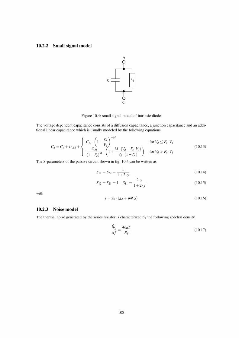
10.2.2 Small signal model
Figure 10.4: small signal model of intrinsic diode
The voltage dependent capacitance consists of a diffusion capacitance, a junction capacitance and an addi-tional linear capacitance which is usually modeled by the following equations.
Cd = Cp + τ ·gd +
C j0 ·
(1− Vd
Vj
)−M
for Vd ≤ Fc ·Vj
C j0
(1−Fc)M ·(
1+M · (Vd−Fc ·Vj)
Vj · (1−Fc)
)for Vd > Fc ·Vj
(10.13)
The S-parameters of the passive circuit shown in fig. 10.4 can be written as
S11 = S22 =1
1+2 ·y(10.14)
S12 = S21 = 1−S11 =2 ·y
1+2 ·y(10.15)
withy = Z0 · (gd + jωCd) (10.16)
10.2.3 Noise modelThe thermal noise generated by the series resistor is characterized by the following spectral density.
i2RS
∆ f=
4kBTRS
(10.17)
108
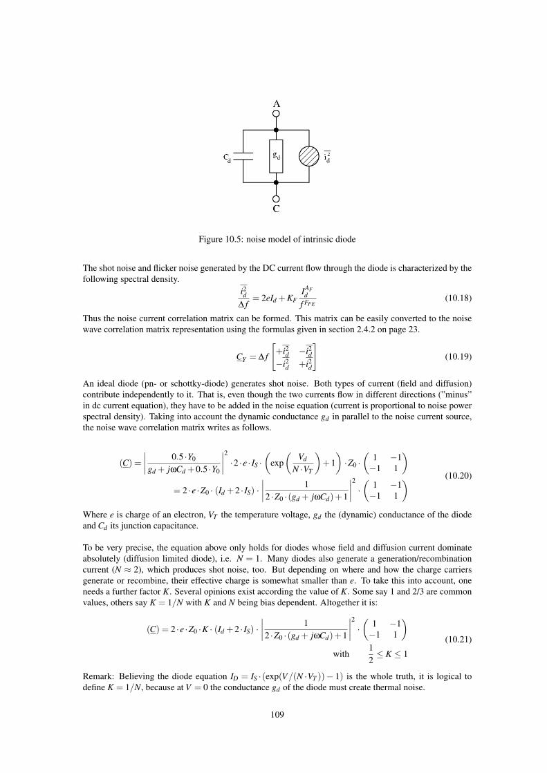
Figure 10.5: noise model of intrinsic diode
The shot noise and flicker noise generated by the DC current flow through the diode is characterized by thefollowing spectral density.
i2d∆ f
= 2eId +KFIAFd
f FFE(10.18)
Thus the noise current correlation matrix can be formed. This matrix can be easily converted to the noisewave correlation matrix representation using the formulas given in section 2.4.2 on page 23.
CY = ∆ f
[+i2d −i2d−i2d +i2d
](10.19)
An ideal diode (pn- or schottky-diode) generates shot noise. Both types of current (field and diffusion)contribute independently to it. That is, even though the two currents flow in different directions (”minus”in dc current equation), they have to be added in the noise equation (current is proportional to noise powerspectral density). Taking into account the dynamic conductance gd in parallel to the noise current source,the noise wave correlation matrix writes as follows.
(C) =∣∣∣∣ 0.5 ·Y0
gd + jωCd +0.5 ·Y0
∣∣∣∣2 ·2 ·e · IS ·(
exp(
Vd
N ·VT
)+1)·Z0 ·
(1 −1−1 1
)= 2 ·e ·Z0 · (Id +2 · IS) ·
∣∣∣∣ 12 ·Z0 ·(gd + jωCd)+1
∣∣∣∣2 · ( 1 −1−1 1
) (10.20)
Where e is charge of an electron, VT the temperature voltage, gd the (dynamic) conductance of the diodeand Cd its junction capacitance.
To be very precise, the equation above only holds for diodes whose field and diffusion current dominateabsolutely (diffusion limited diode), i.e. N = 1. Many diodes also generate a generation/recombinationcurrent (N ≈ 2), which produces shot noise, too. But depending on where and how the charge carriersgenerate or recombine, their effective charge is somewhat smaller than e. To take this into account, oneneeds a further factor K. Several opinions exist according the value of K. Some say 1 and 2/3 are commonvalues, others say K = 1/N with K and N being bias dependent. Altogether it is:
(C) = 2 ·e ·Z0 ·K · (Id +2 · IS) ·∣∣∣∣ 12 ·Z0 ·(gd + jωCd)+1
∣∣∣∣2 · ( 1 −1−1 1
)with
12≤ K ≤ 1
(10.21)
Remark: Believing the diode equation ID = IS ·(exp(V/(N ·VT ))− 1) is the whole truth, it is logical todefine K = 1/N, because at V = 0 the conductance gd of the diode must create thermal noise.
109
Some special diodes have additional current or noise components (tunnel diodes, avalanche diodes etc.).All these mechanisms are not taken into account in equation (10.21).
The parasitic ohmic resistance in a non-ideal diode, of course, creates thermal noise.Noise current correlation matrix (for details on the parameters see above):
(CY ) = 2 ·e ·K · (Id +2 · IS) ·(
1 −1−1 1
)(10.22)
10.2.4 Temperature modelThis section mathematically describes the dependencies of the diode characterictics on temperature. Fora junction diode a typical value for XT I is 3.0, for a Schottky barrier diode it is 2.0. The energy band gapat zero temperature EG is by default 1.11eV. For other materials than Si, 0.69eV (for a Schottky barrierdiode), 0.67eV (for Ge) and 1.43eV (for GaAs) should be used.
n2i (T ) = B ·T 3 ·e−EG(T )/kBT (10.23)
ni (T ) = 1.45 ·1010 ·(
T300K
)1.5
· exp(
e ·EG (300K)2 ·kB ·300K
− e ·EG (T )2 ·kB ·T
)(10.24)
EG (T ) = EG−α ·T 2
β+T(10.25)
with experimental values for Si given by
α = 7.02 ·10−4
β = 1108EG = 1.16eV
The following equations show the temperature dependencies of the diode parameters. The reference tem-perature T1 in these equations denotes the nominal temperature TNOM specified by the diode model.
IS (T2) = IS (T1) ·(
T2
T1
)XT I/N
· exp[−e ·EG (300K)
N ·kB ·T2·(
1− T2
T1
)](10.26)
Vj (T2) =T2
T1·Vj (T1)+
2 ·kB ·T2
e· ln(
ni (T1)ni (T2)
)(10.27)
=T2
T1·Vj (T1)−
2 ·kB ·T2
e· ln(
T2
T1
)1.5
−(
T2
T1·EG (T1)−EG (T2)
)(10.28)
C j0 (T2) = C j0 (T1) ·(
1+M ·(
400 ·10−6 · (T2−T1)−Vj (T2)−Vj (T1)
Vj (T1)
))(10.29)
Some additionial temperature coefficients determine the temperature dependence of even more model pa-rameters.
Bv (T2) = Bv (T1)−TBv · (T2−T1) (10.30)
τ(T2) = τ(T1) ·(
1+Tτ1 · (T2−T1)+Tτ2 · (T2−T1)2)
(10.31)
M (T2) = M (T1) ·(
1+TM1 · (T2−T1)+TM2 · (T2−T1)2)
(10.32)
RS (T2) = RS (T1) · (1+TRS · (T2−T1)) (10.33)
110
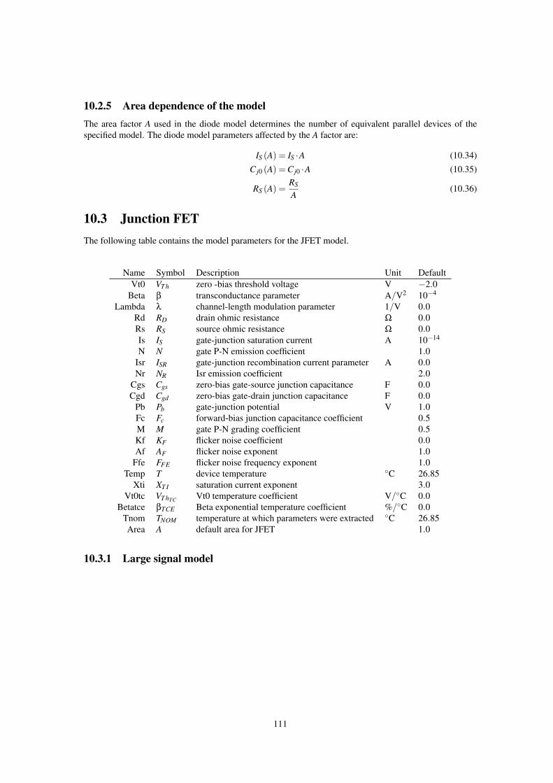
10.2.5 Area dependence of the modelThe area factor A used in the diode model determines the number of equivalent parallel devices of thespecified model. The diode model parameters affected by the A factor are:
IS (A) = IS ·A (10.34)C j0 (A) = C j0 ·A (10.35)
RS (A) =RS
A(10.36)
10.3 Junction FETThe following table contains the model parameters for the JFET model.
Name Symbol Description Unit DefaultVt0 VT h zero -bias threshold voltage V −2.0
Beta β transconductance parameter A/V2 10−4
Lambda λ channel-length modulation parameter 1/V 0.0Rd RD drain ohmic resistance Ω 0.0Rs RS source ohmic resistance Ω 0.0Is IS gate-junction saturation current A 10−14
N N gate P-N emission coefficient 1.0Isr ISR gate-junction recombination current parameter A 0.0Nr NR Isr emission coefficient 2.0
Cgs Cgs zero-bias gate-source junction capacitance F 0.0Cgd Cgd zero-bias gate-drain junction capacitance F 0.0
Pb Pb gate-junction potential V 1.0Fc Fc forward-bias junction capacitance coefficient 0.5M M gate P-N grading coefficient 0.5Kf KF flicker noise coefficient 0.0Af AF flicker noise exponent 1.0
Ffe FFE flicker noise frequency exponent 1.0Temp T device temperature C 26.85
Xti XT I saturation current exponent 3.0Vt0tc VT hTC Vt0 temperature coefficient V/C 0.0
Betatce βTCE Beta exponential temperature coefficient %/C 0.0Tnom TNOM temperature at which parameters were extracted C 26.85Area A default area for JFET 1.0
10.3.1 Large signal model
111
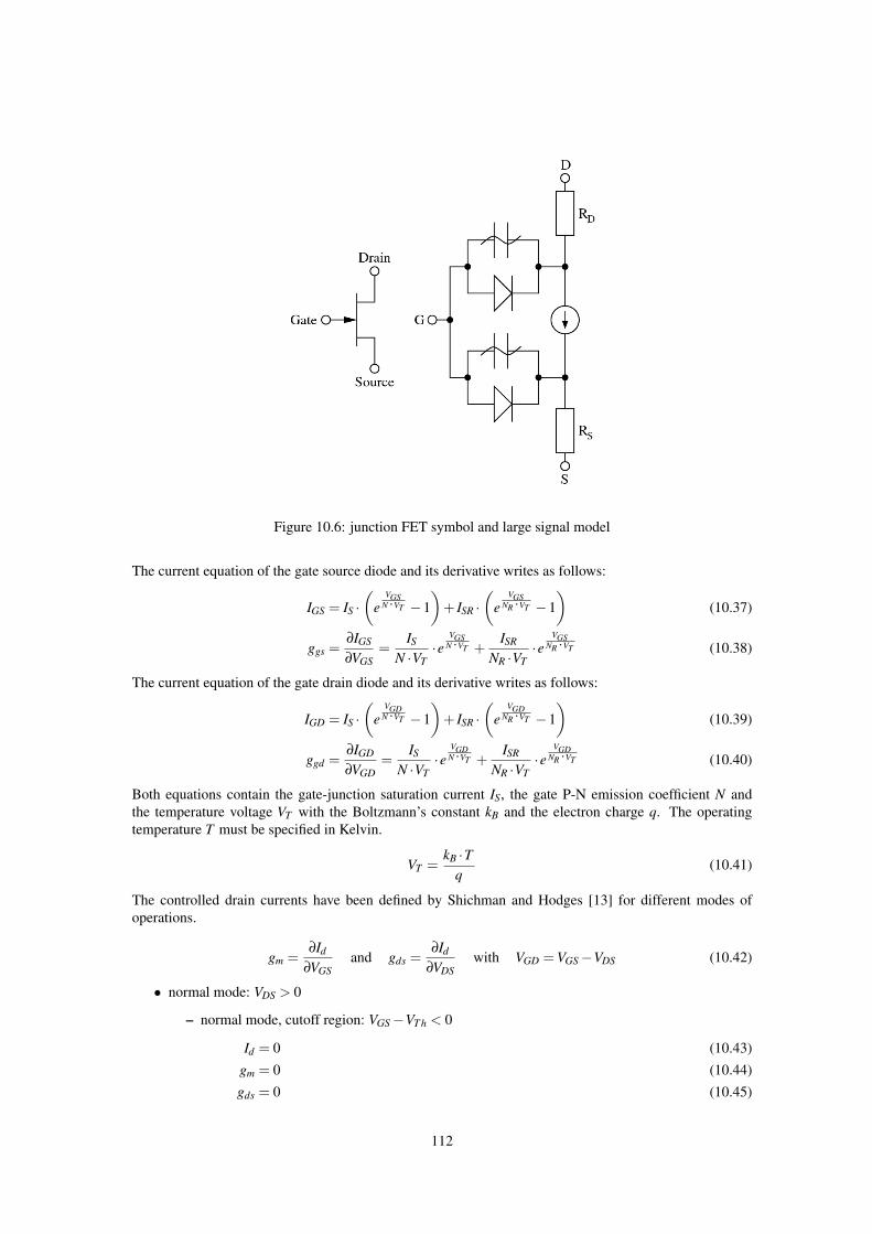
Figure 10.6: junction FET symbol and large signal model
The current equation of the gate source diode and its derivative writes as follows:
IGS = IS ·(
eVGS
N ·VT −1)
+ ISR ·(
eVGS
NR ·VT −1)
(10.37)
ggs =∂IGS
∂VGS=
IS
N ·VT·e
VGSN ·VT +
ISR
NR ·VT·e
VGSNR ·VT (10.38)
The current equation of the gate drain diode and its derivative writes as follows:
IGD = IS ·(
eVGD
N ·VT −1)
+ ISR ·(
eVGD
NR ·VT −1)
(10.39)
ggd =∂IGD
∂VGD=
IS
N ·VT·e
VGDN ·VT +
ISR
NR ·VT·e
VGDNR ·VT (10.40)
Both equations contain the gate-junction saturation current IS, the gate P-N emission coefficient N andthe temperature voltage VT with the Boltzmann’s constant kB and the electron charge q. The operatingtemperature T must be specified in Kelvin.
VT =kB ·T
q(10.41)
The controlled drain currents have been defined by Shichman and Hodges [13] for different modes ofoperations.
gm =∂Id
∂VGSand gds =
∂Id
∂VDSwith VGD = VGS−VDS (10.42)
• normal mode: VDS > 0
– normal mode, cutoff region: VGS−VT h < 0
Id = 0 (10.43)gm = 0 (10.44)gds = 0 (10.45)
112
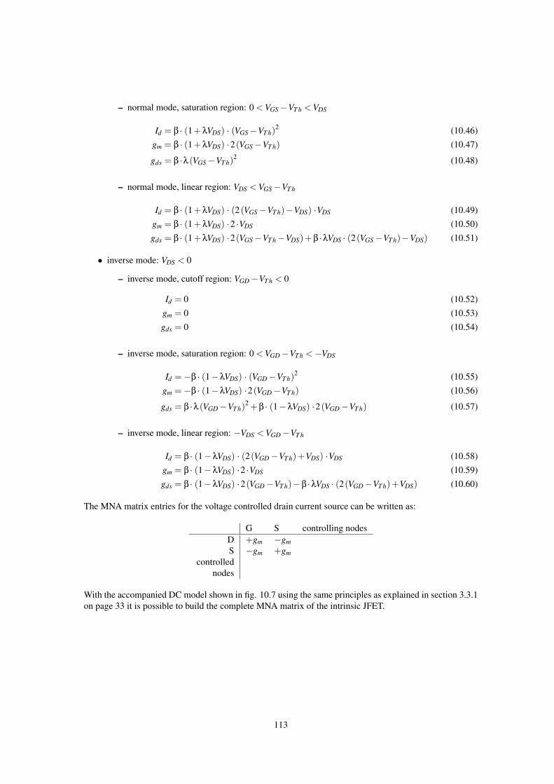
– normal mode, saturation region: 0 < VGS−VT h < VDS
Id = β · (1+λVDS) · (VGS−VT h)2 (10.46)
gm = β · (1+λVDS) ·2(VGS−VT h) (10.47)
gds = β ·λ(VGS−VT h)2 (10.48)
– normal mode, linear region: VDS < VGS−VT h
Id = β · (1+λVDS) · (2(VGS−VT h)−VDS) ·VDS (10.49)gm = β · (1+λVDS) ·2 ·VDS (10.50)gds = β · (1+λVDS) ·2(VGS−VT h−VDS)+β ·λVDS · (2(VGS−VT h)−VDS) (10.51)
• inverse mode: VDS < 0
– inverse mode, cutoff region: VGD−VT h < 0
Id = 0 (10.52)gm = 0 (10.53)gds = 0 (10.54)
– inverse mode, saturation region: 0 < VGD−VT h <−VDS
Id =−β · (1−λVDS) · (VGD−VT h)2 (10.55)
gm =−β · (1−λVDS) ·2(VGD−VT h) (10.56)
gds = β ·λ(VGD−VT h)2 +β · (1−λVDS) ·2(VGD−VT h) (10.57)
– inverse mode, linear region: −VDS < VGD−VT h
Id = β · (1−λVDS) · (2(VGD−VT h)+VDS) ·VDS (10.58)gm = β · (1−λVDS) ·2 ·VDS (10.59)gds = β · (1−λVDS) ·2(VGD−VT h)−β ·λVDS · (2(VGD−VT h)+VDS) (10.60)
The MNA matrix entries for the voltage controlled drain current source can be written as:
G S controlling nodesD +gm −gmS −gm +gm
controllednodes
With the accompanied DC model shown in fig. 10.7 using the same principles as explained in section 3.3.1on page 33 it is possible to build the complete MNA matrix of the intrinsic JFET.
113
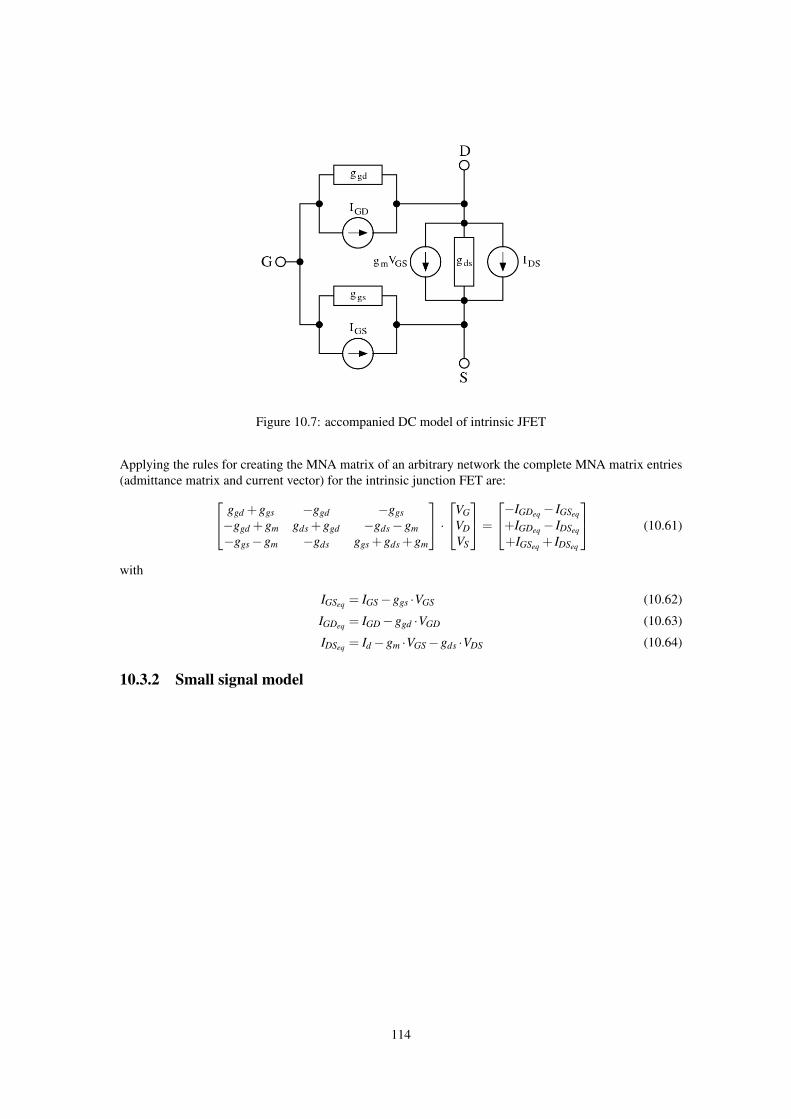
Figure 10.7: accompanied DC model of intrinsic JFET
Applying the rules for creating the MNA matrix of an arbitrary network the complete MNA matrix entries(admittance matrix and current vector) for the intrinsic junction FET are: ggd +ggs −ggd −ggs
−ggd +gm gds +ggd −gds−gm−ggs−gm −gds ggs +gds +gm
·VG
VDVS
=
−IGDeq − IGSeq
+IGDeq − IDSeq
+IGSeq + IDSeq
(10.61)
with
IGSeq = IGS−ggs ·VGS (10.62)
IGDeq = IGD−ggd ·VGD (10.63)
IDSeq = Id−gm ·VGS−gds ·VDS (10.64)
10.3.2 Small signal model
114
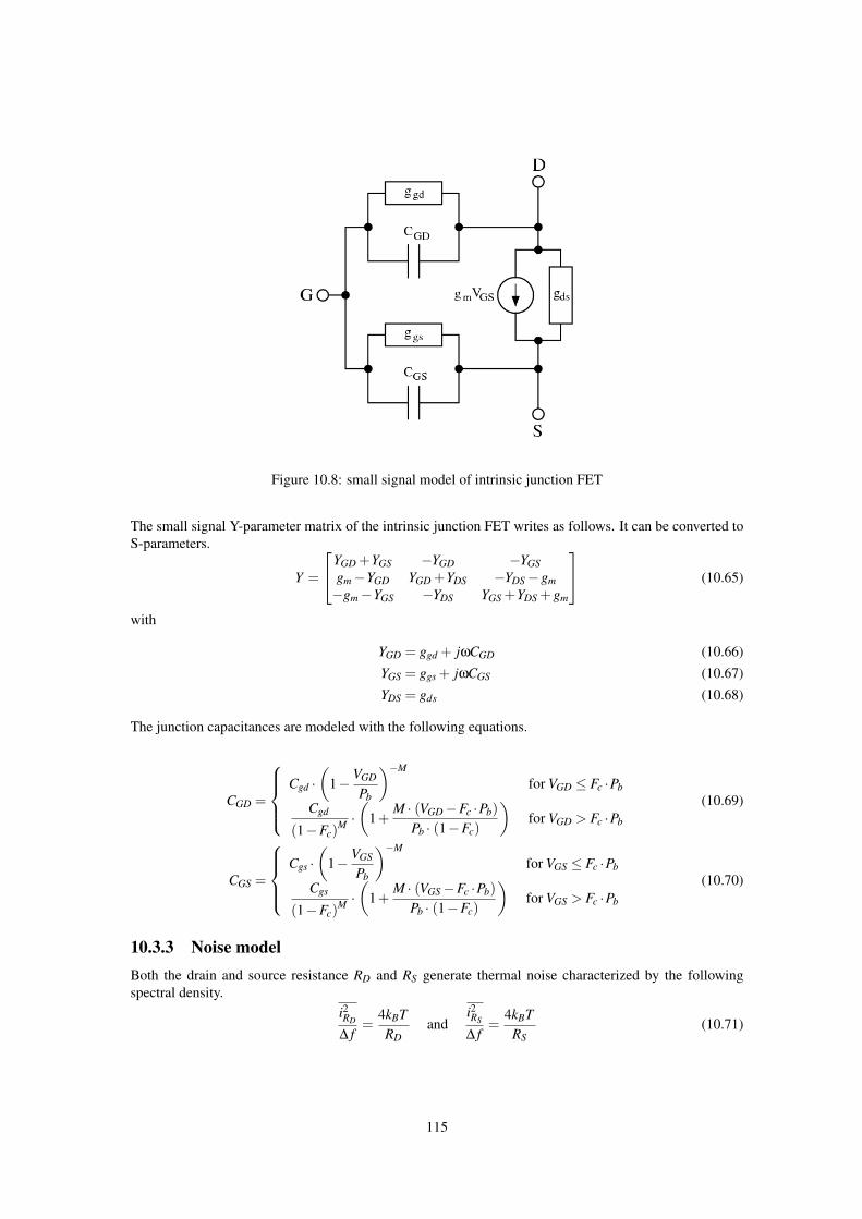
Figure 10.8: small signal model of intrinsic junction FET
The small signal Y-parameter matrix of the intrinsic junction FET writes as follows. It can be converted toS-parameters.
Y =
YGD +YGS −YGD −YGSgm−YGD YGD +YDS −YDS−gm−gm−YGS −YDS YGS +YDS +gm
(10.65)
with
YGD = ggd + jωCGD (10.66)YGS = ggs + jωCGS (10.67)YDS = gds (10.68)
The junction capacitances are modeled with the following equations.
CGD =
Cgd ·
(1− VGD
Pb
)−M
for VGD ≤ Fc ·Pb
Cgd
(1−Fc)M ·(
1+M · (VGD−Fc ·Pb)
Pb · (1−Fc)
)for VGD > Fc ·Pb
(10.69)
CGS =
Cgs ·
(1− VGS
Pb
)−M
for VGS ≤ Fc ·Pb
Cgs
(1−Fc)M ·(
1+M · (VGS−Fc ·Pb)
Pb · (1−Fc)
)for VGS > Fc ·Pb
(10.70)
10.3.3 Noise modelBoth the drain and source resistance RD and RS generate thermal noise characterized by the followingspectral density.
i2RD
∆ f=
4kBTRD
andi2RS
∆ f=
4kBTRS
(10.71)
115
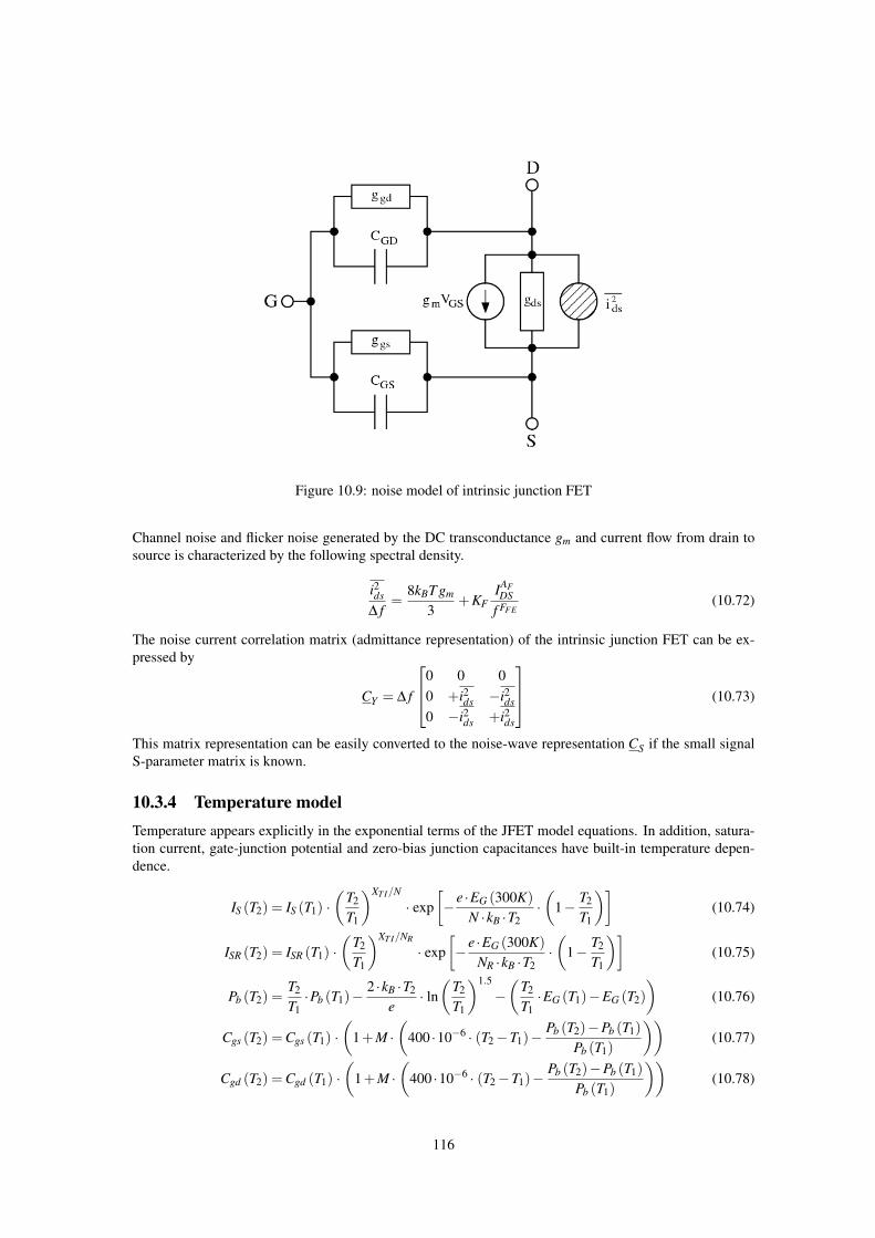
Figure 10.9: noise model of intrinsic junction FET
Channel noise and flicker noise generated by the DC transconductance gm and current flow from drain tosource is characterized by the following spectral density.
i2ds∆ f
=8kBT gm
3+KF
IAFDS
f FFE(10.72)
The noise current correlation matrix (admittance representation) of the intrinsic junction FET can be ex-pressed by
CY = ∆ f
0 0 00 +i2ds −i2ds0 −i2ds +i2ds
(10.73)
This matrix representation can be easily converted to the noise-wave representation CS if the small signalS-parameter matrix is known.
10.3.4 Temperature modelTemperature appears explicitly in the exponential terms of the JFET model equations. In addition, satura-tion current, gate-junction potential and zero-bias junction capacitances have built-in temperature depen-dence.
IS (T2) = IS (T1) ·(
T2
T1
)XT I/N
· exp[−e ·EG (300K)
N ·kB ·T2·(
1− T2
T1
)](10.74)
ISR (T2) = ISR (T1) ·(
T2
T1
)XT I/NR
· exp[−e ·EG (300K)
NR ·kB ·T2·(
1− T2
T1
)](10.75)
Pb (T2) =T2
T1·Pb (T1)−
2 ·kB ·T2
e· ln(
T2
T1
)1.5
−(
T2
T1·EG (T1)−EG (T2)
)(10.76)
Cgs (T2) = Cgs (T1) ·(
1+M ·(
400 ·10−6 · (T2−T1)−Pb (T2)−Pb (T1)
Pb (T1)
))(10.77)
Cgd (T2) = Cgd (T1) ·(
1+M ·(
400 ·10−6 · (T2−T1)−Pb (T2)−Pb (T1)
Pb (T1)
))(10.78)
116
where the EG (T ) dependency has already been described in section 10.2.4 on page 110. Also the thresholdvoltage as well as the transconductance parameter have a temperature dependence determined by
VT h (T2) = VT h (T1)+VT hTC · (T2−T1) (10.79)
β(T2) = β(T1) ·1.01βTCE ·(T2−T1) (10.80)
10.3.5 Area dependence of the modelThe area factor A used for the JFET model determines the number of equivalent parallel devices of aspecified model. The following parameters are affected by the area factor.
β(A) = β ·A IS (A) = IS ·A (10.81)
RD (A) =RD
ARS (A) =
RS
A(10.82)
Cgs (A) = Cgs ·A Cgd (A) = Cgd ·A (10.83)
10.4 Homo-Junction Bipolar TransistorThe following table contains the model parameters for the BJT (Spice Gummel-Poon) model.
Name Symbol Description Unit DefaultIs IS saturation current A 10−16
Nf NF forward emission coefficient 1.0Nr NR reverse emission coefficient 1.0Ikf IKF high current corner for forward beta A ∞
Ikr IKR high current corner for reverse beta A ∞
Vaf VAF forward early voltage V ∞
Var VAR reverse early voltage V ∞
Ise ISE base-emitter leakage saturation current A 0Ne NE base-emitter leakage emission coefficient 1.5Isc ISC base-collector leakage saturation current A 0Nc NC base-collector leakage emission coefficient 2.0Bf BF forward beta 100Br BR reverse beta 1
Rbm RBm minimum base resistance for high currents Ω 0.0Irb IRB current for base resistance midpoint A ∞
Rc RC collector ohmic resistance Ω 0.0Re RE emitter ohmic resistance Ω 0.0Rb RB zero-bias base resistance (may be high-current Ω 0.0
dependent)Cje CJE base-emitter zero-bias depletion capacitance F 0.0Vje VJE base-emitter junction built-in potential V 0.75Mje MJE base-emitter junction exponential factor 0.33Cjc CJC base-collector zero-bias depletion capacitance F 0.0Vjc VJC base-collector junction built-in potential V 0.75Mjc MJC base-collector junction exponential factor 0.33
Xcjc XCJC fraction of Cjc that goes to internal base pin 1.0Cjs CJS zero-bias collector-substrate capacitance F 0.0Vjs VJS substrate junction built-in potential V 0.75Mjs MJS substrate junction exponential factor 0.0
Fc FC forward-bias depletion capacitance coefficient 0.5Tf TF ideal forward transit time s 0.0
117
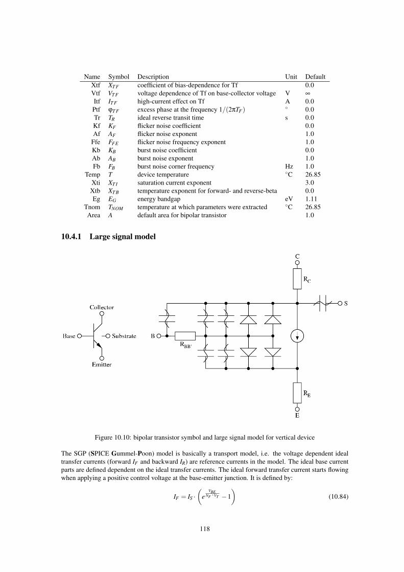
Name Symbol Description Unit DefaultXtf XT F coefficient of bias-dependence for Tf 0.0Vtf VT F voltage dependence of Tf on base-collector voltage V ∞
Itf IT F high-current effect on Tf A 0.0Ptf ϕT F excess phase at the frequency 1/(2πTF) 0.0Tr TR ideal reverse transit time s 0.0Kf KF flicker noise coefficient 0.0Af AF flicker noise exponent 1.0
Ffe FFE flicker noise frequency exponent 1.0Kb KB burst noise coefficient 0.0Ab AB burst noise exponent 1.0Fb FB burst noise corner frequency Hz 1.0
Temp T device temperature C 26.85Xti XT I saturation current exponent 3.0Xtb XT B temperature exponent for forward- and reverse-beta 0.0Eg EG energy bandgap eV 1.11
Tnom TNOM temperature at which parameters were extracted C 26.85Area A default area for bipolar transistor 1.0
10.4.1 Large signal model
Figure 10.10: bipolar transistor symbol and large signal model for vertical device
The SGP (SPICE Gummel-Poon) model is basically a transport model, i.e. the voltage dependent idealtransfer currents (forward IF and backward IR) are reference currents in the model. The ideal base currentparts are defined dependent on the ideal transfer currents. The ideal forward transfer current starts flowingwhen applying a positive control voltage at the base-emitter junction. It is defined by:
IF = IS ·(
eVBE
NF ·VT −1)
(10.84)
118
The ideal base current components are defined by the ideal transfer currents. The non-ideal componentsare independently defined by dedicated saturation currents and emission coefficients.
IBEI =IF
BFgBEI =
∂IBEI
∂VBE=
IS
NF ·VT ·BF·e
VBENF ·VT (10.85)
IBEN = ISE ·(
eVBE
NE ·VT −1)
gBEN =∂IBEN
∂VBE=
ISE
NE ·VT·e
VBENE ·VT (10.86)
IBE = IBEI + IBEN (10.87)gπ = gBE = gBEI +gBEN (10.88)
The ideal backward transfer current arises when applying a positive control voltage at the base-collectorjunction (e.g. in the active inverse mode). It is defined by:
IR = IS ·(
eVBC
NR ·VT −1)
(10.89)
Again, the ideal base current component through the base-collector junction is defined in reference to theideal backward transfer current and the non-ideal component is defined by a dedicated saturation currentand emission coefficient.
IBCI =IR
BRgBCI =
∂IBCI
∂VBC=
IS
NR ·VT ·BR·e
VBCNR ·VT (10.90)
IBCN = ISC ·(
eVBC
NC ·VT −1)
gBCN =∂IBCN
∂VBC=
ISC
NC ·VT·e
VBCNC ·VT (10.91)
IBC = IBCI + IBCN (10.92)gµ = gBC = gBCI +gBCN (10.93)
With these definitions it is possible to calculate the overall base current flowing into the device using allthe base current components.
IB = IBE + IBC = IBEI + IBEN + IBCI + IBCN (10.94)
The overall transfer current IT can be calculated using the normalized base charge QB and the ideal forwardand backward transfer currents.
IT = IT F − IT R =IF − IR
QB(10.95)
The normalized base charge QB has no dimension and has the value 1 for VBE = VBC = 0. It is used tomodel two effects: the influence of the base width modulation on the transfer current (Early effect) and theideal transfer currents deviation at high currents, i.e. the decreasing current gain at high currents.
QB =Q1
2·(
1+√
1+4 ·Q2
)(10.96)
The Q1 term is used to describe the Early effect and Q2 is responsible for the high current effects.
Q1 =1
1− VBC
VAF− VBE
VAR
and Q2 =IF
IKF+
IR
IKR(10.97)
The transfer current IT depends on VBE and VBC by the normalized base charge QB and the forward transfercurrent IF and the backward transfer current IR. That is why both of the partial derivatives are required.
119
The forward transconductance gm f of the transfer current IT is obtained by differentiating it with respect toVBE . The reverse transconductance gmr can be calculated by differentiating the transfer current with respectto VBC.
gm f =∂IT
∂VBE=
∂IT F
∂VBE− ∂IT R
∂VBE=
1QB·(
+gIF − IT ·∂QB
∂VBE
)(10.98)
gmr =∂IT
∂VBC=
∂IT F
∂VBC− ∂IT R
∂VBC=
1QB·(−gIR− IT ·
∂QB
∂VBC
)(10.99)
With gIF being the forward conductance of the ideal forward transfer current and gIR being the reverseconductance of the ideal backward transfer current.
gIF =∂IF
∂VBE= gBEI ·BF (10.100)
gIR =∂IR
∂VBC= gBCI ·BR (10.101)
The remaining derivatives in eq. (10.98), (10.99), (10.119) and (10.120) can be written as
∂QB
∂VBE= Q1 ·
(QB
VAR+
gIF
IKF ·√
1+4 ·Q2
)(10.102)
∂QB
∂VBC= Q1 ·
(QB
VAF+
gIR
IKR ·√
1+4 ·Q2
)(10.103)
For the calculation of the bias dependent base resistance RBB′ there are two different ways within theSGP model. If the model parameter IRB is not given it is determined by the normalized base charge QB.Otherwise IRB specifies the base current at which the base resistance drops half way to the minimum (i.e.the constant component) base resistance RBm.
RBB′ =
RBm +
RB−RBm
QBfor IRB = ∞
RBm +3 · (RB−RBm) · tanz− zz · tan2 z
for IRB 6= ∞
(10.104)
with z =
√1+
144π2 ·
IB
IRB−1
24π2 ·
√IB
IRB
(10.105)
120
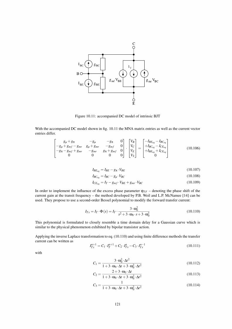
Figure 10.11: accompanied DC model of intrinsic BJT
With the accompanied DC model shown in fig. 10.11 the MNA matrix entries as well as the current vectorentries differ.
gµ +gπ −gµ −gπ 0−gµ +gm f −gmr gµ +gmr −gm f 0−gπ−gm f +gmr −gmr gπ +gm f 0
0 0 0 0
·
VBVCVEVS
=
−IBEeq − IBCeq
+IBCeq − ICEeq
+IBEeq + ICEeq
0
(10.106)
IBEeq = IBE −gπ ·VBE (10.107)
IBCeq = IBC−gµ ·VBC (10.108)
ICEeq = IT −gm f ·VBE +gmr ·VBC (10.109)
In order to implement the influence of the excess phase parameter ϕT F – denoting the phase shift of thecurrent gain at the transit frequency – the method developed by P.B. Weil and L.P. McNamee [14] can beused. They propose to use a second-order Bessel polynomial to modify the forward transfer current:
IT x = IT ·Φ(s) = IT ·3 ·ω2
0
s2 +3 ·ω0 ·s+3 ·ω20
(10.110)
This polynomial is formulated to closely resemble a time domain delay for a Gaussian curve which issimilar to the physical phenomenon exhibited by bipolar transistor action.
Applying the inverse Laplace transformation to eq. (10.110) and using finite difference methods the transfercurrent can be written as
In+1T x = C1 · In+1
T +C2 · InT x−C3 · In−1
T x (10.111)
with
C1 =3 ·ω2
0 ·∆t2
1+3 ·ω0 ·∆t +3 ·ω20 ·∆t2
(10.112)
C2 =2+3 ·ω0 ·∆t
1+3 ·ω0 ·∆t +3 ·ω20 ·∆t2
(10.113)
C3 =1
1+3 ·ω0 ·∆t +3 ·ω20 ·∆t2
(10.114)
121
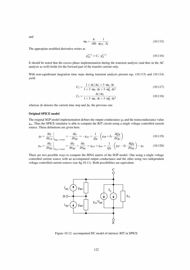
andω0 =
π
180· 1
ϕT F ·TF(10.115)
The appropiate modified derivative writes as
gn+1mx = C1 ·gn+1
m (10.116)
It should be noted that the excess phase implementation during the transient analysis (and thus in the ACanalysis as well) holds for the forward part of the transfer current only.
With non-equidistant inegration time steps during transient analysis present eqs. (10.113) and (10.114)yield
C2 =1+∆t/∆t1 +3 ·ω0 ·∆t
1+3 ·ω0 ·∆t +3 ·ω20 ·∆t2
(10.117)
C3 =∆t/∆t1
1+3 ·ω0 ·∆t +3 ·ω20 ·∆t2
(10.118)
whereas ∆t denotes the current time step and ∆t1 the previous one.
Original SPICE model
The original SGP model implementation defines the output conductance g0 and the transconductance valuegm. Thus the SPICE simulator is able to compute the BJT circuit using a single voltage controlled currentsource. These definitions are given here.
g0 =∂IT
∂VCE
∣∣∣∣VBE=const
=− ∂IT
∂VBC=−gmr =
1QB·(
gIR + IT ·∂QB
∂VBC
)(10.119)
gm =∂IT
∂VBE
∣∣∣∣VCE=const
=∂IT
∂VBE+
∂IT
∂VBC= gm f +gmr =
1QB·(
gIF − IT ·∂QB
∂VBE
)−g0 (10.120)
There are two possible ways to compute the MNA matrix of the SGP model. One using a single voltagecontrolled current source with an accompanied output conductance and the other using two independentvoltage controlled current sources (see fig.10.11). Both possibilities are equivalent.
Figure 10.12: accompanied DC model of intrinsic BJT in SPICE
122
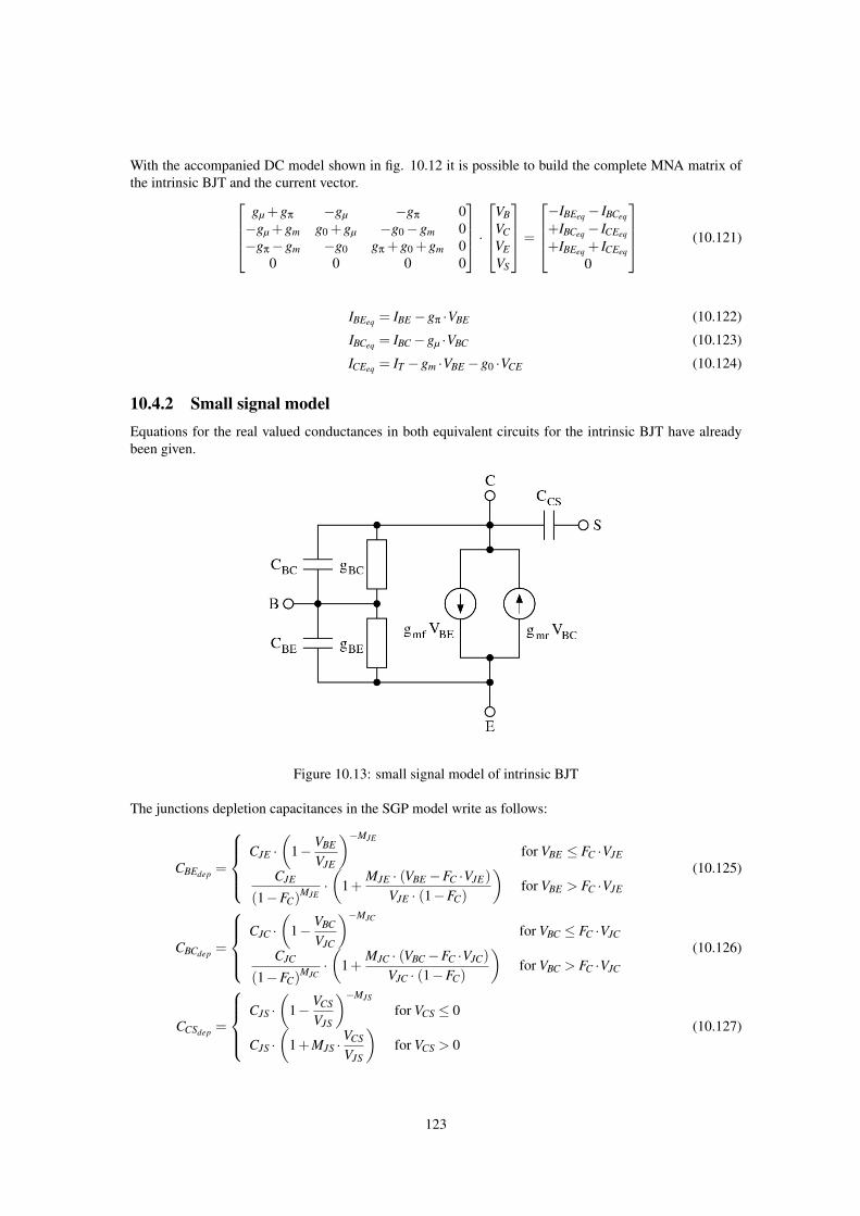
With the accompanied DC model shown in fig. 10.12 it is possible to build the complete MNA matrix ofthe intrinsic BJT and the current vector.
gµ +gπ −gµ −gπ 0−gµ +gm g0 +gµ −g0−gm 0−gπ−gm −g0 gπ +g0 +gm 0
0 0 0 0
·
VBVCVEVS
=
−IBEeq − IBCeq
+IBCeq − ICEeq
+IBEeq + ICEeq
0
(10.121)
IBEeq = IBE −gπ ·VBE (10.122)
IBCeq = IBC−gµ ·VBC (10.123)
ICEeq = IT −gm ·VBE −g0 ·VCE (10.124)
10.4.2 Small signal modelEquations for the real valued conductances in both equivalent circuits for the intrinsic BJT have alreadybeen given.
Figure 10.13: small signal model of intrinsic BJT
The junctions depletion capacitances in the SGP model write as follows:
CBEdep =
CJE ·
(1− VBE
VJE
)−MJE
for VBE ≤ FC ·VJE
CJE
(1−FC)MJE·(
1+MJE · (VBE −FC ·VJE)
VJE · (1−FC)
)for VBE > FC ·VJE
(10.125)
CBCdep =
CJC ·
(1− VBC
VJC
)−MJC
for VBC ≤ FC ·VJC
CJC
(1−FC)MJC·(
1+MJC · (VBC−FC ·VJC)
VJC · (1−FC)
)for VBC > FC ·VJC
(10.126)
CCSdep =
CJS ·
(1− VCS
VJS
)−MJS
for VCS ≤ 0
CJS ·(
1+MJS ·VCS
VJS
)for VCS > 0
(10.127)
123
The base-collector depletion capacitance is split into two components: an external and an internal.
CBCIdep = XCJC ·CBCdep (10.128)
CBCXdep = (1−XCJC) ·CBCdep (10.129)
The base-emitter diffusion capacitance can be obtained using the following equation.
CBEdi f f =∂QBE
∂VBEwith QBE =
IF
QB·TFF (10.130)
Thus the diffusion capacitance depends on the bias-dependent effective forward transit time TFF which isdefined as:
TFF = TF ·
(1+XT F ·
(IF
IF + IT F
)2
· exp(
VBC
1.44 ·VT F
))(10.131)
With∂TFF
∂VBE=
TF ·XT F ·2 ·gIF · IF · IT F
(IF + IT F)3 · exp(
VBC
1.44 ·VT F
)(10.132)
the base-emitter diffusion capacitance can finally be written as:
CBEdi f f =∂QBE
∂VBE=
1QB·(
IF ·∂TFF
∂VBE+TFF ·
(gIF −
IF
QB· ∂QB
∂VBE
))(10.133)
Because the base-emitter charge QBE in eq. (10.130) also depends on the voltage across the base-collectorjunction, it is necessary to find the appropriate derivative as well:
CBEBC =∂QBE
∂VBC=
IF
QB·(
∂TFF
∂VBC− TFF
QB· ∂QB
∂VBC
)(10.134)
which turns out to be a so called transcapacitance. It additionally requires:
∂TFF
∂VBC=
TF ·XT F
1.44 ·VT F·(
IF
IF + IT F
)2
· exp(
VBC
1.44 ·VT F
)(10.135)
The base-collector diffusion capacitance writes as follows:
CBCdi f f =∂QBC
∂VBC= TR ·gIR (10.136)
To take the excess phase parameter ϕT F into account the forward transconductance is going to be a complexquantity.
gm f = gm f ·e− jϕex with ϕex =(
π
180·ϕT F
)·TF ·2π f (10.137)
With these calculations made it is now possible to define the small signal Y-parameters of the intrinsic BJT.The Y-parameter matrix can be converted to S-parameters.
Y =
YBC +YBE +YBEBC −YBC−YBEBC −YBE 0gm f −YBC−gmr YCS +YBC +gmr −gm f −YCS
gmr−gm f −YBE −YBEBC −gmr +YBEBC YBE +gm f 00 −YCS 0 YCS
(10.138)
with
YBC = gµ + jω(
CBCIdep +CBCdi f f
)(10.139)
YBE = gπ + jω(
CBEdep +CBEdi f f
)(10.140)
YCS = jω ·CCSdep (10.141)
YBEBC = jω ·CBEBC (10.142)
The external capacitance CBCX connected between the internal collector node and the external base node isseparately modeled if it is non-zero and if there is a non-zero base resistance.
124
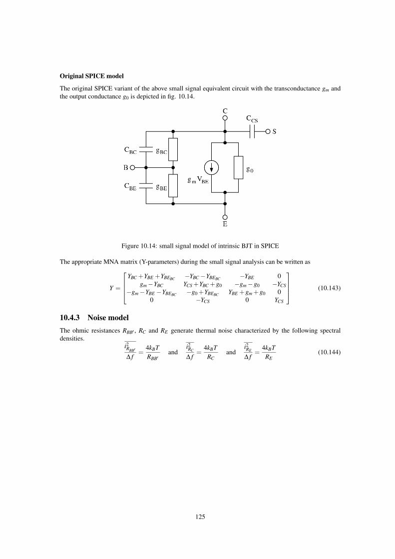
Original SPICE model
The original SPICE variant of the above small signal equivalent circuit with the transconductance gm andthe output conductance g0 is depicted in fig. 10.14.
Figure 10.14: small signal model of intrinsic BJT in SPICE
The appropriate MNA matrix (Y-parameters) during the small signal analysis can be written as
Y =
YBC +YBE +YBEBC −YBC−YBEBC −YBE 0
gm−YBC YCS +YBC +g0 −gm−g0 −YCS−gm−YBE −YBEBC −g0 +YBEBC YBE +gm +g0 0
0 −YCS 0 YCS
(10.143)
10.4.3 Noise modelThe ohmic resistances RBB′ , RC and RE generate thermal noise characterized by the following spectraldensities.
i2RBB′
∆ f=
4kBTRBB′
andi2RC
∆ f=
4kBTRC
andi2RE
∆ f=
4kBTRE
(10.144)
125
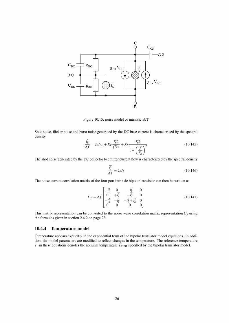
Figure 10.15: noise model of intrinsic BJT
Shot noise, flicker noise and burst noise generated by the DC base current is characterized by the spectraldensity
i2b∆ f
= 2eIBE +KFIAFBE
f FFE+KB
IABBE
1+(
fFB
)2 (10.145)
The shot noise generated by the DC collector to emitter current flow is characterized by the spectral density
i2c∆ f
= 2eIT (10.146)
The noise current correlation matrix of the four port intrinsic bipolar transistor can then be written as
CY = ∆ f
+i2b 0 −i2b 00 +i2c −i2c 0−i2b −i2c +i2c + i2b 00 0 0 0
(10.147)
This matrix representation can be converted to the noise wave correlation matrix representation CS usingthe formulas given in section 2.4.2 on page 23.
10.4.4 Temperature modelTemperature appears explicitly in the exponential term of the bipolar transistor model equations. In addi-tion, the model parameters are modified to reflect changes in the temperature. The reference temperatureT1 in these equations denotes the nominal temperature TNOM specified by the bipolar transistor model.
126
IS (T2) = IS (T1) ·(
T2
T1
)XT I
· exp[−e ·EG (300K)
kB ·T2·(
1− T2
T1
)](10.148)
VJE (T2) =T2
T1·VJE (T1)−
2 ·kB ·T2
e· ln(
T2
T1
)1.5
−(
T2
T1·EG (T1)−EG (T2)
)(10.149)
VJC (T2) =T2
T1·VJC (T1)−
2 ·kB ·T2
e· ln(
T2
T1
)1.5
−(
T2
T1·EG (T1)−EG (T2)
)(10.150)
VJS (T2) =T2
T1·VJS (T1)−
2 ·kB ·T2
e· ln(
T2
T1
)1.5
−(
T2
T1·EG (T1)−EG (T2)
)(10.151)
where the EG (T ) dependency has already been described in section 10.2.4 on page 110. The temperaturedependence of BF and BR is determined by
BF (T2) = BF (T1) ·(
T2
T1
)XT B
(10.152)
BR (T2) = BR (T1) ·(
T2
T1
)XT B
(10.153)
Through the parameters ISE and ISC, respectively, the temperature dependence of the non-ideal saturationcurrents is determined by
ISE (T2) = ISE (T1) ·(
T2
T1
)−XT B
·[
IS (T2)IS (T1)
]1/NE
(10.154)
ISC (T2) = ISC (T1) ·(
T2
T1
)−XT B
·[
IS (T2)IS (T1)
]1/NC
(10.155)
The temperature dependence of the zero-bias depletion capacitances CJE , CJC and CJS are determined by
CJE (T2) = CJE (T1) ·(
1+MJE ·(
400 ·10−6 · (T2−T1)−VJE (T2)−VJE (T1)
VJE (T1)
))(10.156)
CJC (T2) = CJC (T1) ·(
1+MJC ·(
400 ·10−6 · (T2−T1)−VJC (T2)−VJC (T1)
VJC (T1)
))(10.157)
CJS (T2) = CJS (T1) ·(
1+MJS ·(
400 ·10−6 · (T2−T1)−VJS (T2)−VJS (T1)
VJS (T1)
))(10.158)
10.4.5 Area dependence of the modelThe area factor A used in the bipolar transistor model determines the number of equivalent parallel devicesof a specified model. The bipolar transistor model parameters affected by the A factor are:
IS (A) = IS ·A (10.159)ISE (A) = ISE ·A ISC (A) = ISC ·A (10.160)IKF (A) = IKF ·A IKR (A) = IKR ·A (10.161)IRB (A) = IRB ·A IT F (A) = IT F ·A (10.162)
CJE (A) = CJE ·A CJC (A) = CJC ·A (10.163)CJS (A) = CJS ·A (10.164)
RB (A) =RB
ARBm (A) =
RBm
A(10.165)
RE (A) =RE
ARC (A) =
RC
A(10.166)
127
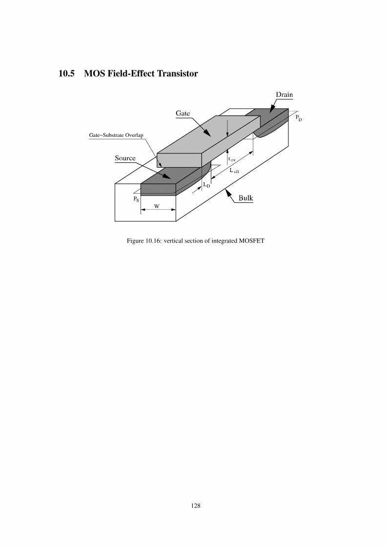
10.5 MOS Field-Effect Transistor
Figure 10.16: vertical section of integrated MOSFET
128
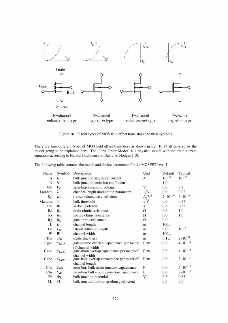
Figure 10.17: four types of MOS field effect transistors and their symbols
There are four different types of MOS field effect transistors as shown in fig. 10.17 all covered by themodel going to be explained here. The “First Order Model” is a physical model with the drain currentequations according to Harold Shichman and David A. Hodges [13].
The following table contains the model and device parameters for the MOSFET level 1.
Name Symbol Description Unit Default TypicalIs IS bulk junction saturation current A 10−14 10−15
N N bulk junction emission coefficient 1.0Vt0 VT 0 zero-bias threshold voltage V 0.0 0.7
Lambda λ channel-length modulation parameter 1/V 0.0 0.02Kp KP transconductance coefficient A/V2 2 ·10−5 6 ·10−5
Gamma γ bulk threshold√
V 0.0 0.37Phi Φ surface potential V 0.6 0.65Rd RD drain ohmic resistance Ω 0.0 1.0Rs RS source ohmic resistance Ω 0.0 1.0Rg RG gate ohmic resistance Ω 0.0
L L channel length m 100µ
Ld LD lateral diffusion length m 0.0 10−7
W W channel width m 100µ
Tox TOX oxide thickness m 0.1µ 2 ·10−8
Cgso CGSO gate-source overlap capacitance per meterof channel width
F/m 0.0 4 ·10−11
Cgdo CGDO gate-drain overlap capacitance per meter ofchannel width
F/m 0.0 4 ·10−11
Cgbo CGBO gate-bulk overlap capacitance per meter ofchannel length
F/m 0.0 2 ·10−10
Cbd CBD zero-bias bulk-drain junction capacitance F 0.0 6 ·10−17
Cbs CBS zero-bias bulk-source junction capacitance F 0.0 6 ·10−17
Pb ΦB bulk junction potential V 0.8 0.87Mj MJ bulk junction bottom grading coefficient 0.5 0.5
129
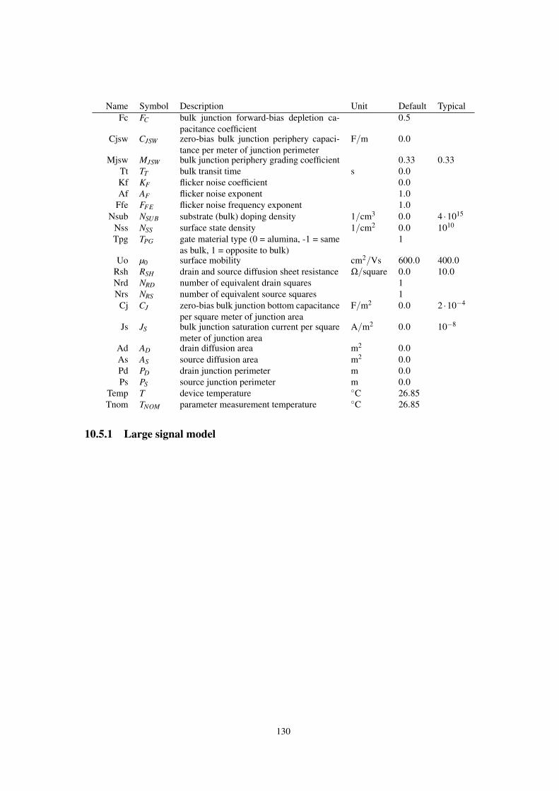
Name Symbol Description Unit Default TypicalFc FC bulk junction forward-bias depletion ca-
pacitance coefficient0.5
Cjsw CJSW zero-bias bulk junction periphery capaci-tance per meter of junction perimeter
F/m 0.0
Mjsw MJSW bulk junction periphery grading coefficient 0.33 0.33Tt TT bulk transit time s 0.0Kf KF flicker noise coefficient 0.0Af AF flicker noise exponent 1.0
Ffe FFE flicker noise frequency exponent 1.0Nsub NSUB substrate (bulk) doping density 1/cm3 0.0 4 ·1015
Nss NSS surface state density 1/cm2 0.0 1010
Tpg TPG gate material type (0 = alumina, -1 = sameas bulk, 1 = opposite to bulk)
1
Uo µ0 surface mobility cm2/Vs 600.0 400.0Rsh RSH drain and source diffusion sheet resistance Ω/square 0.0 10.0Nrd NRD number of equivalent drain squares 1Nrs NRS number of equivalent source squares 1Cj CJ zero-bias bulk junction bottom capacitance
per square meter of junction areaF/m2 0.0 2 ·10−4
Js JS bulk junction saturation current per squaremeter of junction area
A/m2 0.0 10−8
Ad AD drain diffusion area m2 0.0As AS source diffusion area m2 0.0Pd PD drain junction perimeter m 0.0Ps PS source junction perimeter m 0.0
Temp T device temperature C 26.85Tnom TNOM parameter measurement temperature C 26.85
10.5.1 Large signal model
130
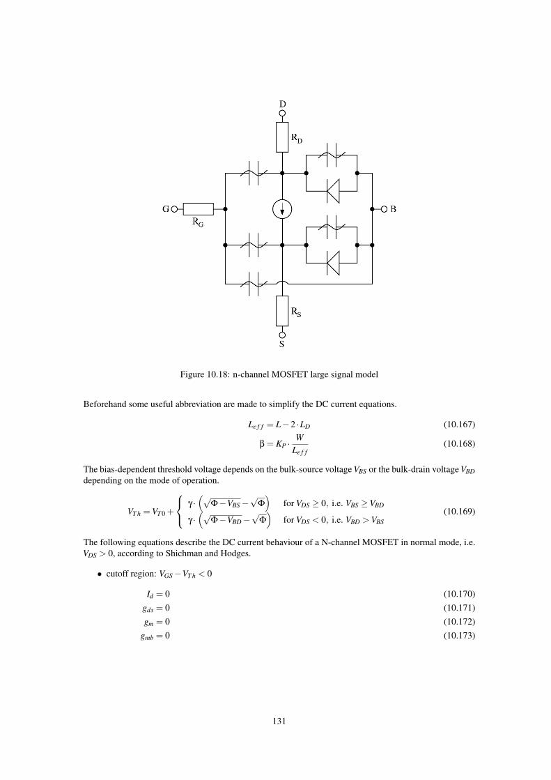
Figure 10.18: n-channel MOSFET large signal model
Beforehand some useful abbreviation are made to simplify the DC current equations.
Le f f = L−2 ·LD (10.167)
β = KP ·W
Le f f(10.168)
The bias-dependent threshold voltage depends on the bulk-source voltage VBS or the bulk-drain voltage VBDdepending on the mode of operation.
VT h = VT 0 +
γ ·(√
Φ−VBS−√
Φ
)for VDS ≥ 0, i.e. VBS ≥VBD
γ ·(√
Φ−VBD−√
Φ
)for VDS < 0, i.e. VBD > VBS
(10.169)
The following equations describe the DC current behaviour of a N-channel MOSFET in normal mode, i.e.VDS > 0, according to Shichman and Hodges.
• cutoff region: VGS−VT h < 0
Id = 0 (10.170)gds = 0 (10.171)gm = 0 (10.172)
gmb = 0 (10.173)
131
• saturation region: 0 < VGS−VT h < VDS
Id = β/2 · (1+λVDS) · (VGS−VT h)2 (10.174)
gds = β/2 ·λ(VGS−VT h)2 (10.175)
gm = β · (1+λVDS)(VGS−VT h) (10.176)
gmb = gm ·γ
2√
Φ−VBS(10.177)
• linear region: VDS < VGS−VT h
Id = β · (1+λVDS) · (VGS−VT h−VDS/2) ·VDS (10.178)gds = β · (1+λVDS) · (VGS−VT h−VDS)+β ·λVDS · (VGS−VT h−VDS/2) (10.179)gm = β · (1+λVDS) ·VDS (10.180)
gmb = gm ·γ
2√
Φ−VBS(10.181)
with
gds =∂Id
∂VDSand gm =
∂Id
∂VGSand gmb =
∂Id
∂VBS(10.182)
In the inverse mode of operation, i.e. VDS < 0, the same equations can be applied with the followingmodifications. Replace VBS with VBD, VGS with VGD and VDS with−VDS. The drain current Id gets reversed.Furthermore the transconductances alter their controlling nodes, i.e.
gm =∂Id
∂VGDand gmb =
∂Id
∂VBD(10.183)
The current equations of the two parasitic diodes at the bulk node and their derivatives write as follows.
IBD = ISD ·(
eVBD
N ·VT −1)
gbd =∂IBD
∂VBD=
ISD
N ·VT·e
VBDN ·VT (10.184)
IBS = ISS ·(
eVBS
N ·VT −1)
gbs =∂IBS
∂VBS=
ISS
N ·VT·e
VBSN ·VT (10.185)
withISD = IS and ISS = IS (10.186)
132
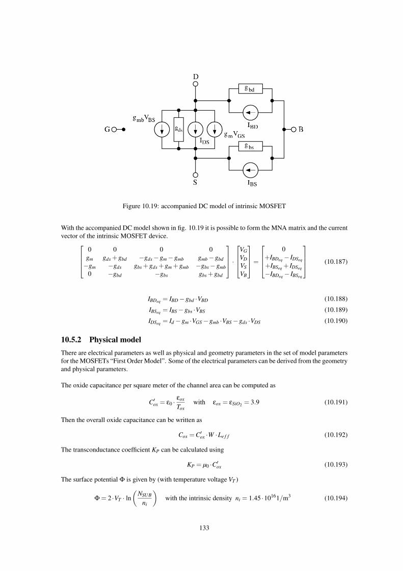
Figure 10.19: accompanied DC model of intrinsic MOSFET
With the accompanied DC model shown in fig. 10.19 it is possible to form the MNA matrix and the currentvector of the intrinsic MOSFET device.
0 0 0 0gm gds +gbd −gds−gm−gmb gmb−gbd−gm −gds gbs +gds +gm +gmb −gbs−gmb
0 −gbd −gbs gbs +gbd
·
VGVDVSVB
=
0
+IBDeq − IDSeq
+IBSeq + IDSeq
−IBDeq − IBSeq
(10.187)
IBDeq = IBD−gbd ·VBD (10.188)
IBSeq = IBS−gbs ·VBS (10.189)
IDSeq = Id−gm ·VGS−gmb ·VBS−gds ·VDS (10.190)
10.5.2 Physical modelThere are electrical parameters as well as physical and geometry parameters in the set of model parametersfor the MOSFETs “First Order Model”. Some of the electrical parameters can be derived from the geometryand physical parameters.
The oxide capacitance per square meter of the channel area can be computed as
C′ox = ε0 ·εox
Toxwith εox = εSiO2 = 3.9 (10.191)
Then the overall oxide capacitance can be written as
Cox = C′ox ·W ·Le f f (10.192)
The transconductance coefficient KP can be calculated using
KP = µ0 ·C′ox (10.193)
The surface potential Φ is given by (with temperature voltage VT )
Φ = 2 ·VT · ln(
NSUB
ni
)with the intrinsic density ni = 1.45 ·10161/m3 (10.194)
133
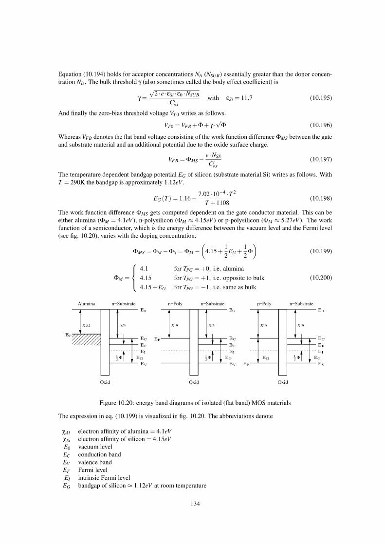
Equation (10.194) holds for acceptor concentrations NA (NSUB) essentially greater than the donor concen-tration ND. The bulk threshold γ (also sometimes called the body effect coefficient) is
γ =√
2 ·e ·εSi ·ε0 ·NSUB
C′oxwith εSi = 11.7 (10.195)
And finally the zero-bias threshold voltage VT 0 writes as follows.
VT 0 = VFB +Φ+ γ ·√
Φ (10.196)
Whereas VFB denotes the flat band voltage consisting of the work function difference ΦMS between the gateand substrate material and an additional potential due to the oxide surface charge.
VFB = ΦMS−e ·NSS
C′ox(10.197)
The temperature dependent bandgap potential EG of silicon (substrate material Si) writes as follows. WithT = 290K the bandgap is approximately 1.12eV .
EG (T ) = 1.16− 7.02 ·10−4 ·T 2
T +1108(10.198)
The work function difference ΦMS gets computed dependent on the gate conductor material. This can beeither alumina (ΦM = 4.1eV ), n-polysilicon (ΦM ≈ 4.15eV ) or p-polysilicon (ΦM ≈ 5.27eV ). The workfunction of a semiconductor, which is the energy difference between the vacuum level and the Fermi level(see fig. 10.20), varies with the doping concentration.
ΦMS = ΦM−ΦS = ΦM−(
4.15+12
EG +12
Φ
)(10.199)
ΦM =
4.1 for TPG = +0, i.e. alumina4.15 for TPG = +1, i.e. opposite to bulk4.15+EG for TPG =−1, i.e. same as bulk
(10.200)
Figure 10.20: energy band diagrams of isolated (flat band) MOS materials
The expression in eq. (10.199) is visualized in fig. 10.20. The abbreviations denote
χAl electron affinity of alumina = 4.1eVχSi electron affinity of silicon = 4.15eVE0 vacuum levelEC conduction bandEV valence bandEF Fermi levelEI intrinsic Fermi level
EG bandgap of silicon ≈ 1.12eV at room temperature
134
Please note that the potential 1/2 ·Φ is positive in p-MOS and negative in n-MOS as the following equationreveals.
ΦF =EF −EI
e(10.201)
When the gate conductor material is a heavily doped polycrystalline silicon (also called polysilicon) thenthe model assumes that the Fermi level of this semiconductor is the same as the conduction band (for n-poly) or the valence band (for p-poly). In alumina the Fermi level, valence and conduction band all equalthe electron affinity.
If the zero-bias bulk junction bottom capacitance per square meter of junction area CJ is not given it can becomputed as follows.
CJ =√
εSi ·ε0 ·e ·NSUB
2 ·ΦB(10.202)
That’s it for the physical parameters. The geometry parameters account for the electrical parameters perlength, area or volume. Thus the MOS model is scalable.
The diffusion resistances at drain and gate are computed as follows. The sheet resistance RSH refers to thethickness of the diffusion area.
RD = NRD ·RSH and RS = NRS ·RSH (10.203)
If the bulk junction saturation current per square meter of the junction area JS and the drain and sourceareas are given the according saturation currents are calculated with the following equations.
ISD = AD ·JS and ISS = AS ·JS (10.204)
If the parameters CBD and CBS are not given the zero-bias depletion capacitances for the bottom and sidewallcapacitances are computed as follows.
CBD = CJ ·AD (10.205)CBS = CJ ·AS (10.206)
CBDS = CJSW ·PD (10.207)CBSS = CJSW ·PS (10.208)
10.5.3 Small signal model
135
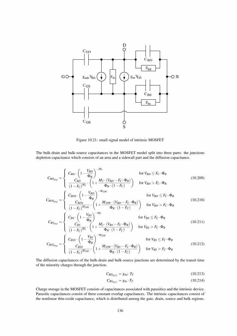
Figure 10.21: small signal model of intrinsic MOSFET
The bulk-drain and bulk-source capacitances in the MOSFET model split into three parts: the junctionsdepletion capacitance which consists of an area and a sidewall part and the diffusion capacitance.
CBDdep =
CBD ·
(1− VBD
ΦB
)−MJ
for VBD ≤ FC ·ΦB
CBD
(1−FC)MJ·(
1+MJ · (VBD−FC ·ΦB)
ΦB · (1−FC)
)for VBD > FC ·ΦB
(10.209)
CBDSdep =
CBDS ·
(1− VBD
ΦB
)−MJSW
for VBD ≤ FC ·ΦB
CBDS
(1−FC)MJSW·(
1+MJSW · (VBD−FC ·ΦB)
ΦB · (1−FC)
)for VBD > FC ·ΦB
(10.210)
CBSdep =
CBS ·
(1− VBS
ΦB
)−MJ
for VBS ≤ FC ·ΦB
CBS
(1−FC)MJ·(
1+MJ · (VBS−FC ·ΦB)
ΦB · (1−FC)
)for VBS > FC ·ΦB
(10.211)
CBSSdep =
CBSS ·
(1− VBS
ΦB
)−MJSW
for VBS ≤ FC ·ΦB
CBSS
(1−FC)MJSW·(
1+MJSW · (VBS−FC ·ΦB)
ΦB · (1−FC)
)for VBS > FC ·ΦB
(10.212)
The diffusion capacitances of the bulk-drain and bulk-source junctions are determined by the transit timeof the minority charges through the junction.
CBDdi f f = gbd ·TT (10.213)
CBSdi f f = gbs ·TT (10.214)
Charge storage in the MOSFET consists of capacitances associated with parasitics and the intrinsic device.Parasitic capacitances consist of three constant overlap capacitances. The intrinsic capacitances consist ofthe nonlinear thin-oxide capacitance, which is distributed among the gate, drain, source and bulk regions.
136
The MOS gate capacitances, as a nonlinear function of the terminal voltages, are modeled by J.E. Meyer’spiece-wise linear model [15].
The bias-dependent gate-oxide capacitances distribute according to the Meyer model [15] as follows.
• cutoff regions: VGS−VT h < 0
– VGS−VT h ≤−Φ
CGS = 0 (10.215)CGD = 0 (10.216)CGB = Cox (10.217)
– −Φ < VGS−VT h ≤−Φ/2
CGS = 0 (10.218)CGD = 0 (10.219)
CGB =−Cox ·VGS−VT h
Φ(10.220)
– −Φ/2 < VGS−VT h ≤ 0
CGS =23·Cox +
43·Cox ·
VGS−VT h
Φ(10.221)
CGD = 0 (10.222)
CGB =−Cox ·VGS−VT h
Φ(10.223)
• saturation region: 0 < VGS−VT h < VDS
CGS =23·Cox (10.224)
CGD = 0 (10.225)CGB = 0 (10.226)
• linear region: VDS < VGS−VT h
CGS =23·Cox ·
(1− (VDsat −VDS)
2
(2 ·VDsat −VDS)2
)(10.227)
CGD =23·Cox ·
(1− V 2
Dsat
(2 ·VDsat −VDS)2
)(10.228)
CGB = 0 (10.229)
with
VDsat =
VGS−VT h for VGS−VT h > 00 otherwise
(10.230)
In the inverse mode of operation VGS and VGD need to be exchanged, VDS changes its sign, then the aboveformulas can be applied as well.
137
The constance overlap capacitances compute as follows.
CGSOV L = CGSO ·W (10.231)CGDOV L = CGDO ·W (10.232)CGBOV L = CGBO ·Le f f (10.233)
With these definitions it is possible to form the small signal Y-parameter matrix of the intrinsic MOSFETdevice in an operating point which can be converted into S-parameters.
Y =
YGS +YGD +
YGB
−YGD −YGS −YGB
gm−YGD YGD +YBD +YDS −YDS−gm−gmb −YBD +gmb−gm−YGS −YDS YGS +YDS +
YBS +gm +gmb
−YBS−gmb
−YGB −YBD −YBS YBD +YBS +YGB
(10.234)
with
YGS = jω(CGS +CGSOV L) (10.235)YGD = jω(CGD +CGDOV L) (10.236)YGB = jω(CGB +CGBOV L) (10.237)
YBD = gbd + jω(
CBDdep +CBDSdep +CBDdi f f
)(10.238)
YBS = gbs + jω(
CBSdep +CBSSdep +CBSdi f f
)(10.239)
YDS = gds (10.240)
10.5.4 Noise modelThe thermal noise generated by the external resistors RG, RS and RD is characterized by the followingspectral density.
i2RG
∆ f=
4kBTRG
andi2RD
∆ f=
4kBTRD
andi2RS
∆ f=
4kBTRS
(10.241)
138
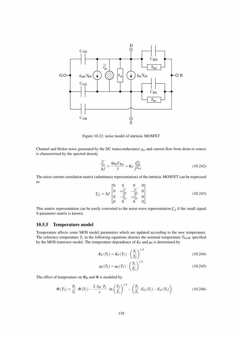
Figure 10.22: noise model of intrinsic MOSFET
Channel and flicker noise generated by the DC transconductance gm and current flow from drain to sourceis characterized by the spectral density
i2ds∆ f
=8kBT gm
3+KF
IAFDS
f FFE(10.242)
The noise current correlation matrix (admittance representation) of the intrinsic MOSFET can be expressedas
CY = ∆ f
0 0 0 00 +i2ds −i2ds 00 −i2ds +i2ds 00 0 0 0
(10.243)
This matrix representation can be easily converted to the noise-wave representation CS if the small signalS-parameter matrix is known.
10.5.5 Temperature modelTemperature affects some MOS model parameters which are updated according to the new temperature.The reference temperature T1 in the following equations denotes the nominal temperature TNOM specifiedby the MOS transistor model. The temperature dependence of KP and µ0 is determined by
KP (T2) = KP (T1) ·(
T1
T2
)1.5
(10.244)
µ0 (T2) = µ0 (T1) ·(
T1
T2
)1.5
(10.245)
The effect of temperature on ΦB and Φ is modeled by
Φ(T2) =T2
T1·Φ(T1)−
2 ·kB ·T2
e· ln(
T2
T1
)1.5
−(
T2
T1·EG (T1)−EG (T2)
)(10.246)
139
where the EG (T ) dependency has already been described in section 10.2.4 on page 110. The temperaturedependence of CBD, CBS, CJ and CJSW is described by the following relations
CBD (T2) = CBD (T1) ·(
1+MJ ·(
400 ·10−6 · (T2−T1)−ΦB (T2)−ΦB (T1)
ΦB (T1)
))(10.247)
CBS (T2) = CBS (T1) ·(
1+MJ ·(
400 ·10−6 · (T2−T1)−ΦB (T2)−ΦB (T1)
ΦB (T1)
))(10.248)
CJ (T2) = CJ (T1) ·(
1+MJ ·(
400 ·10−6 · (T2−T1)−ΦB (T2)−ΦB (T1)
ΦB (T1)
))(10.249)
CJSW (T2) = CJSW (T1) ·(
1+MJSW ·(
400 ·10−6 · (T2−T1)−ΦB (T2)−ΦB (T1)
ΦB (T1)
))(10.250)
The temperature dependence of IS is given by the relation
IS (T2) = IS (T1) · exp[− e
kB ·T2·(
T2
T1·EG (T1)−EG (T2)
)](10.251)
An analogue dependence holds for JS.
10.6 Models for boolean devicesLogical (boolean) functions (OR, AND, XOR etc.) can be modeled using macro models. Here, each inputgets the transfer characteristic and its derivative described as follows:
ui = tanh(10 ·(uin−0.5)) (10.252)
u′i = 10 ·(1− tanh2(10 ·(uin−0.5))
)(10.253)
The resulting voltages ui for each input are combined to create the wanted function for a device with Ninputs:
Inverter: uout = 0.5 ·(1−ui) (10.254)
NOR: uout =N
∑m
21−ui,m
(10.255)
OR: uout = 1−uout,NOR (10.256)
AND: uout =N
∑m
21+ui,m
(10.257)
NAND: uout = 1−uout,AND (10.258)
XOR: uout = 0.5 ·(
1−∏m−ui,m
)(10.259)
XNOR: uout = 0.5 ·(
1+∏m
ui,m
)(10.260)
The above-mentioned functions model devices with 0V as logical low-level and 1V as logical high-level.Of course, they can be easily transformed into higher voltage levels by multiplying the desired high-levelvoltage to the output voltage uout and dividing the input voltages uin by the desired high-level voltage.Note: The derivatives also get uin divided by the desired high-level voltage, but they are not multiplied bythe desired high-level voltage.
140
To perform a simulation on these devices, the first derivatives are also needed:
Inverter:∂uout
∂uin=−0.5 ·u′i (10.261)
OR:∂uout
∂uin,n=
2 ·N ·u′i,n((1−ui,n) · ∑
m
21−ui,m
)2 (10.262)
NOR:∂uout
∂uin,n=− ∂uout
∂uin,n
∣∣∣∣OR
(10.263)
AND:∂uout
∂uin,n=
2 ·N ·u′i,n((1+ui,n) · ∑
m
21+ui,m
)2 (10.264)
NAND:∂uout
∂uin,n=− ∂uout
∂uin,n
∣∣∣∣AND
(10.265)
XOR:∂uout
∂uin,n= 0.5 ·u′i,n · ∏
m 6=n−ui,m (10.266)
XNOR:∂uout
∂uin,n= 0.5 ·u′i,n · ∏
m 6=nui,m (10.267)
A problem of these macro models are the numbers of input ports. The output voltage levels worsen withincreasing number of ports. The practical limit lies around eight input ports.
With that knowledge it is now easy to create the MNA matrix. The first port is the output port of the device.So, for a 2-input port device, it is:
. . . 1
. . . 0
. . . 0−1 ∂uout/∂uin,1 ∂uout/∂uin,1 0
·
VoutVin,1Vin,2Iout
=
I0I1I20
(10.268)
The above MNA matrix entries are also used during the non-linear DC and transient analysis with the 0 inthe right hand side vector replaced by an equivalent voltage
Veq =∂uout
∂uin,1·Vin,1 +
∂uout
∂uin,2·Vin,2−uout (10.269)
with uout computed using equations (10.254) to (10.260).
With the given small-signal matrix representation, building the S-parameters is easy.
(S) =
−1 4 ·∂uout/∂uin,1 4 ·∂uout/∂uin,20 1 00 0 1
(10.270)
These matrices can easily extended to any number of input ports.
10.7 Equation defined modelsOften it will happen that a user needs to implement his own model. Therefore, it is useful to supply devicesthat are defined by arbitrary equations.
141
10.7.1 Models with Explicit EquationsFor example the user must enter an equation i(V ) describing how the port current I depends on the portvoltage V = V1−V2 and an equation q(V ) describing how much charge Q is held due to the voltage V .These are time domain equations. The most simple way then is a device with two nodes. Defining
I = i(V ) and g =∂I∂V
= limh→0
I(V +h)− I(V )h
(10.271)
as well as
Q = q(V ) and c =∂Q∂V
= limh→0
Q(V +h)−Q(V )h
(10.272)
the MNA matrix for a (non-linear) DC analysis writes:
[+g(m) −g(m)
−g(m) +g(m)
]·
[V (m+1)
1
V (m+1)2
]=[−I(m) +g(m) ·V (m)
+I(m)−g(m) ·V (m)
]
=
[−I(m) +g(m) ·(V (m)
1 −V (m)2 )
+I(m)−g(m) ·(V (m)1 −V (m)
2 )
] (10.273)
For a transient simulation, equation (6.89) on page 57 has to be used with Q and c.
For an AC analysis the MNA matrix writes:
(Y ) = (g+ jω ·c) ·[+1 −1−1 +1
](10.274)
And the S-parameter matrix writes:
S11 = S22 =1
2 ·Z0 ·Y +1(10.275)
S12 = S21 = 1−S11 (10.276)Y = g+ jω ·c (10.277)
The simulator needs to create the derivatives g and c by its own. This can be done numerically or symboli-cally. One might ask why the non-linear capacitance is modeled as charge, not as capacitance. Indeed thismay be changed, but with a computer algorithm, creating the derivative is easier than to integrate.
The component described above can be expanded to one with two ports (two pairs of terminals: terminal 1and 2 and terminal 3 and 4). That is, the currents and charges of both ports depend on both port voltagesV12 = V1−V2 and V34 = V3−V4. Thus, the defining equations are:
I1 = i1(V12,V34) and g11 =∂I1
∂V12and g12 =
∂I1
∂V34(10.278)
I2 = i2(V12,V34) and g21 =∂I2
∂V12and g22 =
∂I2
∂V34(10.279)
as well as
Q1 = q1(V12,V34) and c11 =∂Q1
∂V12and c12 =
∂Q1
∂V34(10.280)
Q2 = q2(V12,V34) and c21 =∂Q2
∂V12and c22 =
∂Q2
∂V34(10.281)
The MNA matrix for the DC analysis writes:
142
+g(m)
11 −g(m)11 +g(m)
12 −g(m)12
−g(m)11 +g(m)
11 −g(m)12 +g(m)
12
+g(m)21 −g(m)
21 +g(m)22 −g(m)
22
−g(m)21 +g(m)
21 −g(m)22 +g(m)
22
·
V (m+1)1
V (m+1)2
V (m+1)3
V (m+1)4
=
−I(m)
1 +g(m)11 ·V
(m)12 +g(m)
12 ·V(m)34
+I(m)1 −g(m)
11 ·V(m)12 −g(m)
12 ·V(m)34
−I(m)2 +g(m)
21 ·V(m)12 +g(m)
22 ·V(m)34
+I(m)2 −g(m)
21 ·V(m)12 −g(m)
22 ·V(m)34
(10.282)
For a transient simulation, the DC equations have to be extended by the non-linear (trans-) capacitances,e.g. for backward Euler:
In+1,mC11 =
c11(Vn+1,m12 )hn︸ ︷︷ ︸
geq,11
·V n+112 −
c11(V n12)
hn ·V n12︸ ︷︷ ︸
Ieq,11
(10.283)
In+1,mC12 =
c12(Vn+1,m12 )hn︸ ︷︷ ︸
geq,12
·V n+112 −
c12(V n12)
hn ·V n12︸ ︷︷ ︸
Ieq,12
(10.284)
In+1,mC21 =
c21(Vn+1,m34 )hn︸ ︷︷ ︸
geq,21
·V n+134 −
c21(V n34)
hn ·V n34︸ ︷︷ ︸
Ieq,21
(10.285)
In+1,mC22 =
c22(Vn+1,m34 )hn︸ ︷︷ ︸
geq,22
·V n+134 −
c22(V n34)
hn ·V n34︸ ︷︷ ︸
Ieq,22
(10.286)
So with gtr = g+geq it is:+g(m)
tr,11 −g(m)tr,11 +g(m)
tr,12 −g(m)tr,12
−g(m)tr,11 +g(m)
tr,11 −g(m)tr,12 +g(m)
tr,12
+g(m)tr,21 −g(m)
tr,21 +g(m)tr,22 −g(m)
tr,22
−g(m)tr,21 +g(m)
tr,21 −g(m)tr,22 +g(m)
tr,22
·
V (n+1,m+1)1
V (n+1,m+1)2
V (n+1,m+1)3
V (n+1,m+1)4
=
−I(m)
1 +g(m)11 ·V
(m)12 +g(m)
12 ·V(m)34 − I(n)
eq,11− I(n)eq,12
+I(m)1 −g(m)
11 ·V(m)12 −g(m)
12 ·V(m)34 + I(n)
eq,12 + I(n)eq,12
−I(m)2 +g(m)
21 ·V(m)12 +g(m)
22 ·V(m)34 − I(n)
eq,21− I(n)eq,22
+I(m)2 −g(m)
21 ·V(m)12 −g(m)
22 ·V(m)34 + I(n)
eq,21 + I(n)eq,22
(10.287)
For an AC analysis the MNA matrix writes:
(Y ) =
+g11 + jω ·c11 −g11− jω ·c11 +g12 + jω ·c12 −g12− jω ·c12−g11− jω ·c11 +g11 + jω ·c11 −g12− jω ·c12 +g12 + jω ·c12+g21 + jω ·c21 −g21− jω ·c21 +g22 + jω ·c22 −g22− jω ·c22−g21− jω ·c21 +g21 + jω ·c21 −g22− jω ·c22 +g22 + jω ·c22
(10.288)
As can bee seen, this scheme can be expanded to any number of ports. The matrices soon become quitecomplex, but fortunately modern computers are able to cope with this complexity. S-parameters must beobtained numerical by setting equation 10.288 into equation 15.7.
10.7.2 Models with Implicit EquationsThe above-mentioned explicit models are not useable for all components. If the Y-parameters do not existor if the equations cannot be analytically transformed into the explicit form, then an implicit representationmust be taken. hat is, for a one-port (two-terminal) component the following formulas are defined by theuser:
143
0 = f (V, I) and gV =∂ f (V, I)
∂V= lim
h→0
f (V +h, I)− f (V, I)h
(10.289)
and gI =∂ f (V, I)
∂I= lim
h→0
f (V, I +h)− f (V, I)h
(10.290)
The MNA matrix for the AC analysis writes as follows: . . +1. . −1
+gV −gV gI
·V1
V2Iout
=
000
(10.291)
As usual, for the DC analysis the last zero on the right hand side has to be replaced by the iteration formula:
gV ·(V1−V2)+gI · Iout − f (V1−V2, Iout) (10.292)
The S-parameters are:
S11 = S22 =gI
gI−2 ·Z0 ·gV(10.293)
S12 = S21 = 1−S11 (10.294)
Consequently, for a two-port device two equation are necessary: One for first port and one for second port:
0 = f1(V12,V34, I1, I2) (10.295)0 = f2(V12,V34, I1, I2) (10.296)
Building the MNA matrix is again straight forward:
. . . . +1 0. . . . −1 0. . . . 0 +1. . . . 0 −1
+g f 1,V 12 −g f 1,V 12 +g f 1,V 34 −g f 1,V 34 g f 1,I1 g f 1,I2+g f 2,V 12 −g f 2,V 12 +g f 2,V 34 −g f 2,V 34 g f 2,I1 g f 2,I2
·
V (m+1)1
V (m+1)2
V (m+1)3
V (m+1)4
I(m+1)out1
I(m+1)out2
=[
g f 1,V 12 ·V12 +g f 1,V 34 ·V34 +g f 1,I1 · Iout1 +g f 1,I2 · Iout2− f1(V12,V34, Iout1, Iout2)g f 2,V 12 ·V12 +g f 2,V 34 ·V34 +g f 2,I1 · Iout1 +g f 2,I2 · Iout2− f2(V12,V34, Iout1, Iout2)
](10.297)
Once more, this concept can easily expanded to any number of ports. It is also possible mix implicit andexplicit definitions, i.e. some ports of the device may be defined by explicit equations whereas the othersare defined by implicit equations.
The calculation of the S-parameters is not that trival. The Y-parameters as well as the Z-parameters mightbe infinite. A small trick can avoid this problem, as will be shown in the following 2-port example. First,the small-signal Y-parameters should be derived by using the law about implicit functions:
(J) =(
y11 y12y21 y22
)=−
∂ f1
∂I1
∂ f1
∂I2∂ f2
∂I1
∂ f2
∂I2
︸ ︷︷ ︸
Ji
−1
·
∂ f1
∂V1
∂ f1
∂V2∂ f2
∂V1
∂ f2
∂V2
︸ ︷︷ ︸
Jv
(10.298)
The equation reveals immediately the difficulty: The inverse of the current Jocobi matrix Ji may not exist.But this problem can be outsourced to one single scalar number by using Cramer’s rule for matrix inversion:
144
J−1i =
1∆Ji·AJi (10.299)
The matrix AJi is built of the sub-determinantes of Ji in the way that a(n,m) is the determinante of Ji withoutrow m and without column n but multiplied with (−1)n+m. It therefore always exists, whereas dividing bythe determinante of Ji may become infinity. Now parameters can be defined as follows:
(J′) =(
y′11 y′12y′21 y′22
)=−AJi ·Jv (10.300)
Before converting to S-parameters the matrix must be expanded to a 4-port matrix, because the 2-ports arenot referenced to ground:
(J′′) =
+y′11 −y′11 +y′12 −y′12−y′11 +y′11 −y′12 +y′12+y′21 −y′21 +y′22 −y′22−y′21 +y′21 −y′22 +y′22
=−A′Ji ·J′v (10.301)
Finally, equation (15.7) converts the parameters to S-parameters:
(S) = ((E)−Z0 ·(Y )) · ((E)+Z0 ·(Y ))−1 (10.302)
=(
(E)+Z0 ·1
∆Ji·A′Ji ·J′v
)·(
(E)−Z0 ·1
∆Ji·A′Ji ·J′v
)−1
(10.303)
=(∆Ji ·(E)+Z0 ·A′Ji ·J′v
)·(∆Ji ·(E)−Z0 ·A′Ji ·J′v
)−1 (10.304)
The calculations proofs that the critical factor 1/∆Ji disappears and a solution exists if and only if theS-parameters of this device exist.
145
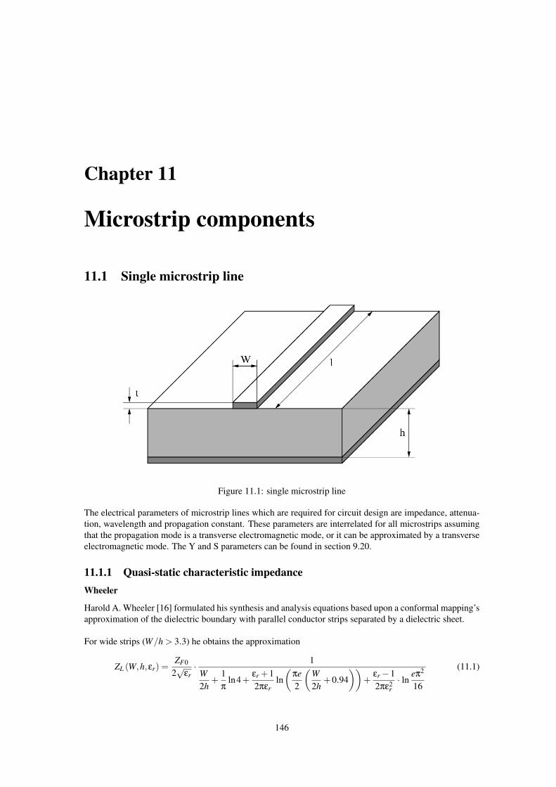
Chapter 11
Microstrip components
11.1 Single microstrip line
Figure 11.1: single microstrip line
The electrical parameters of microstrip lines which are required for circuit design are impedance, attenua-tion, wavelength and propagation constant. These parameters are interrelated for all microstrips assumingthat the propagation mode is a transverse electromagnetic mode, or it can be approximated by a transverseelectromagnetic mode. The Y and S parameters can be found in section 9.20.
11.1.1 Quasi-static characteristic impedanceWheeler
Harold A. Wheeler [16] formulated his synthesis and analysis equations based upon a conformal mapping’sapproximation of the dielectric boundary with parallel conductor strips separated by a dielectric sheet.
For wide strips (W/h > 3.3) he obtains the approximation
ZL (W,h,εr) =ZF0
2√
εr· 1
W2h
+1π
ln4+εr +12πεr
ln(
πe2
(W2h
+0.94))
+εr−12πε2
r· ln eπ2
16
(11.1)
146
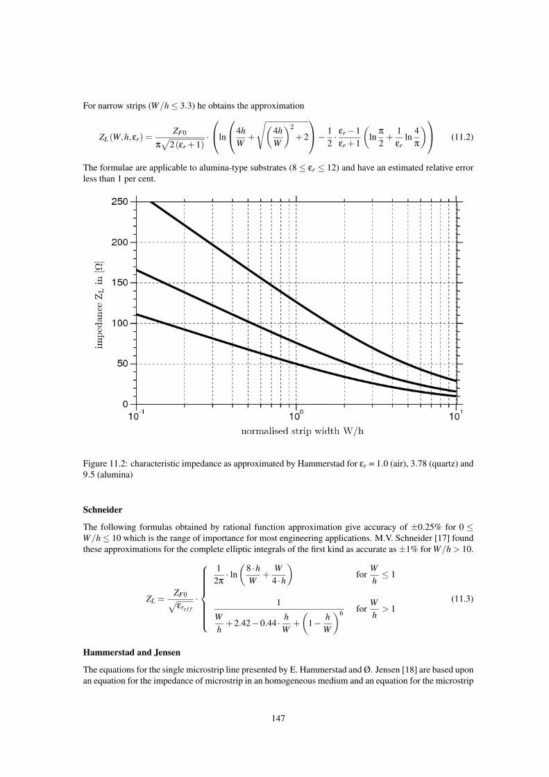
For narrow strips (W/h≤ 3.3) he obtains the approximation
ZL (W,h,εr) =ZF0
π√
2(εr +1)·
ln
4hW
+
√(4hW
)2
+2
− 12· εr−1
εr +1
(ln
π
2+
1εr
ln4π
) (11.2)
The formulae are applicable to alumina-type substrates (8 ≤ εr ≤ 12) and have an estimated relative errorless than 1 per cent.
Figure 11.2: characteristic impedance as approximated by Hammerstad for εr = 1.0 (air), 3.78 (quartz) and9.5 (alumina)
Schneider
The following formulas obtained by rational function approximation give accuracy of ±0.25% for 0 ≤W/h≤ 10 which is the range of importance for most engineering applications. M.V. Schneider [17] foundthese approximations for the complete elliptic integrals of the first kind as accurate as ±1% for W/h > 10.
ZL =ZF0√εre f f
·
12π· ln(
8 ·hW
+W4 ·h
)for
Wh≤ 1
1
Wh
+2.42−0.44 · hW
+(
1− hW
)6 forWh
> 1(11.3)
Hammerstad and Jensen
The equations for the single microstrip line presented by E. Hammerstad and Ø. Jensen [18] are based uponan equation for the impedance of microstrip in an homogeneous medium and an equation for the microstrip
147
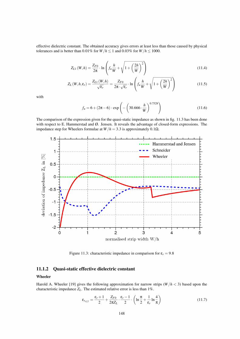
effective dielectric constant. The obtained accuracy gives errors at least less than those caused by physicaltolerances and is better than 0.01% for W/h≤ 1 and 0.03% for W/h≤ 1000.
ZL1 (W,h) =ZF0
2π· ln
fuh
W+
√1+(
2hW
)2 (11.4)
ZL (W,h,εr) =ZL1 (W,h)√
εr=
ZF0
2π ·√
εr· ln
fuh
W+
√1+(
2hW
)2 (11.5)
with
fu = 6+(2π−6) · exp
(−(
30.666 · hW
)0.7528)
(11.6)
The comparison of the expression given for the quasi-static impedance as shown in fig. 11.3 has been donewith respect to E. Hammerstad and Ø. Jensen. It reveals the advantage of closed-form expressions. Theimpedance step for Wheelers formulae at W/h = 3.3 is approximately 0.1Ω.
Figure 11.3: characteristic impedance in comparison for εr = 9.8
11.1.2 Quasi-static effective dielectric constantWheeler
Harold A. Wheeler [19] gives the following approximation for narrow strips (W/h < 3) based upon thecharacteristic impedance ZL. The estimated relative error is less than 1%.
εre f f =εr +1
2+
ZF0
2πZL· εr−1
2·(
lnπ
2+
1εr
ln4π
)(11.7)
148
For narrow strips (W/h≤ 1.3):
εre f f =1+ εr
2·(
AA−B
)2
(11.8)
with
A = ln(
8h
W
)+
132·(
Wh
)2
(11.9)
B =12· εr−1
εr +1·(
lnπ
2+
1εr
ln4π
)(11.10)
For wide strips (W/h > 1.3):
εre f f = εr ·(
E−DE
)2
(11.11)
with
D =εr−12πεr
·(
ln(
πe2
(W2h
+0.94))− 1
εrln
eπ2
16
)(11.12)
E =12·W
h+
1π· ln(
πeWh
+16.0547)
(11.13)
Schneider
The approximate function found by M.V. Schneider [17] is meant to have an accuracy of±2% for εre f f andan accuracy of ±1% for
√εre f f .
εre f f =εr +1
2+
εr−12· 1√
1+10h
W
(11.14)
Hammerstad and Jensen
The accuracy of the E. Hammerstad and Ø. Jensen [18] model is better than 0.2% at least for εr < 128 and0.01≤W/h≤ 100.
εre f f (W,h,εr) =εr +1
2+
εr−12·(
1+10h
W
)−ab
(11.15)
with
a(u) = 1+1
49· ln
(u4 +(u/52)2
u4 +0.432
)+
118.7
· ln(
1+( u
18.1
)3)
(11.16)
b(εr) = 0.564 ·(
εr−0.9εr +3
)0.053
(11.17)
u =Wh
(11.18)
11.1.3 Strip thickness correctionThe formulas given for the quasi-static characteristic impedance and effective dielectric constant in theprevious sections are based upon an infinite thin microstrip line thickness t = 0. A finite thickness t canbe compensated by a reduction of width. That means a strip with the width W and the finite thickness tappears to be a wider strip.
149
Wheeler
Harold A. Wheeler [19] proposes the following equation to account for the strip thickness effect based onfree space without dielectric.
∆W1 =tπ
ln4e√( t
h
)2+(
1/π
W/t +1.10
) (11.19)
For the mixed media case with dielectric he obtains the approximation
∆Wr =12
∆W1
(1+
1εr
)(11.20)
Schneider
M.V. Schneider [17] derived the following approximate expressions.
∆W =
tπ·(
1+ ln4 ·π ·W
t
)for
Wh≤ 1
2π
tπ·(
1+ ln2 ·h
t
)for
Wh
>1
2π
(11.21)
Additional restrictions for applying these expressions are t h, t < W/2 and t/∆W < 0.75. Notice alsothat the ratio ∆W/t is divergent for t→ 0.
Hammerstad and Jensen
E. Hammerstad and Ø. Jensen are using the method described by Wheeler [19] to account for a non-zerostrip thickness. However, some modifications in his equations have been made, which give better accuracyfor narrow strips and for substrates with low dielectric constant. For the homogeneous media the correctionis
∆W1 =t
h ·πln
1+4e
th· coth2√6.517W
(11.22)
and for the mixed media the correction is
∆Wr =12
∆W1
(1+ sech
√εr−1
)(11.23)
By defining corrected strip widths, W1 = W +∆W1 and Wr = W +∆Wr, the effect of strip thickness may beincluded in the equations (11.4) and (11.15).
ZL (W,h, t,εr) =ZL1 (Wr,h)√
εre f f (Wr,h,εr)(11.24)
εre f f (W,h, t,εr) = εre f f (Wr,h,εr) ·(
ZL1 (W1,h)ZL1 (Wr,h)
)2
(11.25)
11.1.4 DispersionDispersion can be a strong effect in microstrip transmission lines due to their inhomogeneity. Typically, asfrequency is increased, εre f f increases in a non-linear manner, approaching an asymptotic value. Dispersionaffects characteristic impedance in a similar way.
150
Kirschning and Jansen
The dispersion formulae given by Kirschning and Jansen [20] is meant to have an accuracy better than0.6% in the range 0.1≤W/h≤ 100, 1≤ εr ≤ 20 and 0≤ h/λ0 ≤ 0.13, i.e. up to about 60GHz for 25mmsubstrates.
εr( f ) = εr−εr− εre f f
1+P( f )(11.26)
with
P( f ) = P1P2 · ((0.1844+P3P4) · fn)1.5763 (11.27)
P1 = 0.27488+
(0.6315+
0.525
(1+0.0157 · fn)20
)·W
h−0.065683 · exp
(−8.7513
Wh
)(11.28)
P2 = 0.33622 · (1− exp(−0.03442 ·εr)) (11.29)
P3 = 0.0363 · exp(−4.6
Wh
)·
(1− exp
(−(
fn
38.7
)4.97))
(11.30)
P4 = 1+2.751 ·(
1− exp(−(
εr
15.916
)8))
(11.31)
fn = f ·h = normalised frequency in [GHz ·mm] (11.32)
Dispersion of the characteristic impedance according to [21] can be applied for the range 0≤ h/λ0 ≤ 0.1,0.1≤W/h≤ 10 and for substrates with 1≤ εr ≤ 18 and is is given by the following set of equations.
R1 = 0.03891 ·ε1.4r (11.33)
R2 = 0.267 ·u7.0 (11.34)
R3 = 4.766 · exp(−3.228 ·u0.641
)(11.35)
R4 = 0.016+(0.0514 ·εr)4.524 (11.36)
R5 = ( fn/28.843)12.0 (11.37)
R6 = 22.20 ·u1.92 (11.38)
and
R7 = 1.206−0.3144 · exp(−R1) · (1− exp(−R2)) (11.39)
R8 = 1+1.275 ·(
1− exp(−0.004625 ·R3 ·ε1.674
r
)· ( fn/18.365)2.745
)(11.40)
R9 = 5.086 · R4 ·R5
0.3838+0.386 ·R4· exp(−R6)
1+1.2992 ·R5· (εr−1)6
1+10 · (εr−1)6 (11.41)
151
and
R10 = 0.00044 ·ε2.136r +0.0184 (11.42)
R11 =( fn/19.47)6
1+0.0962 · ( fn/19.47)6 (11.43)
R12 =1
1+0.00245 ·u2 (11.44)
R13 = 0.9408 ·εr( f )R8 −0.9603 (11.45)
R14 = (0.9408−R9) ·εR8re f f−0.9603 (11.46)
R15 = 0.707 ·R10 · ( fn/12.3)1.097 (11.47)
R16 = 1+0.0503 ·ε2r ·R11 ·
(1− exp
(−(u/15)6
))(11.48)
R17 = R7 ·(
1−1.1241 · R12
R16· exp
(−0.026 · f 1.15656
n −R15
))(11.49)
Finally the frequency-dependent characteristic impedance can be written as
ZL( fn) = ZL(0) ·(
R13
R14
)R17
(11.50)
The abbreviations used in these expressions are fn for the normalized frequency as denoted in eq. (11.32)and u = W/h for the microstrip width normalised with respect to the substrate height. The terms ZL(0) andεre f f denote the static values of microstrip characteristic impedance and effective dielectric constant. Thevalue εr( f ) is the frequency dependent effective dielectric constant computed according to [20].
R.H. Jansen and M. Kirschning remark in [21] for the implementation of the expressions on a computer,R1, R2 and R6 should be restricted to numerical values less or equal 20 in order to prevent overflow.
Yamashita
The values obtained by the approximate dispersion formula as given by E. Yamashita [22] deviate within1% in a wide frequency range compared to the integral equation method used to derive the functionalapproximation. The formula assumes the knowledge of the quasi-static effective dielectric constant. Theapplicable ranges of the formula are 2 < εr < 16, 0.06 <W/h < 16 and 0.1GHz < f < 100GHz. Though thelowest usable frequency is limited by 0.1GHz, the propagation constant for frequencies less than 0.1GHzhas been given as the quasi-static one.
εr( f ) = εre f f ·
1+14·k ·F1.5
1+14·F1.5
2
(11.51)
with
k =
√εr
εre f f
(11.52)
F =4 ·h · f ·
√εr−1
c0·
(0.5+
(1+2 · log
(1+
Wh
))2)
(11.53)
Kobayashi
The dispersion formula presented by M. Kobayashi [23], derived by comparison to a numerical model, hasa high degree of accuracy, better than 0.6% in the range 0.1 ≤W/h ≤ 10, 1 < εr ≤ 128 and any h/λ0 (no
152
frequency limits).
εr( f ) = εr−εr− εre f f
1+(
ff50
)m (11.54)
with
f50 =c0
2π ·h ·(
0.75+(
0.75− 0.332ε1.73
r
)Wh
) · arctan
(εr ·√
εre f f −1εr− εre f f
)√
εr− εre f f
(11.55)
m = m0 ·mc (≤ 2.32) (11.56)
m0 = 1+1
1+√
Wh
+0.32 ·
1
1+√
Wh
3
(11.57)
mc =
1+
1.4
1+Wh
·(
0.15−0.235 · exp(−0.45
ff50
))for W/h≤ 0.7
1 for W/h≥ 0.7
(11.58)
Getsinger
Based upon measurements of dispersion curves for microstrip lines on alumina substrates 0.025 and 0.050inch thick W. J. Getsinger [24] developed a very simple , closed-form expression that allow slide-ruleprediction of microstrip dispersion.
εr( f ) = εr−εr− εre f f
1+G ·(
ffp
)2 (11.59)
with
fp =ZL
2µ0h(11.60)
G = 0.6+0.009 ·ZL (11.61)
Also based upon measurements of microstrip lines 0.1, 0.25 and 0.5 inch in width on a 0.250 inch thick alu-mina substrate Getsinger [25] developed two different dispersion models for the characteristic impedance.
• wave impedance model published in [25]
ZL( f ) = ZL ·
√εre f f
εr( f )(11.62)
• group-delay model published in [26]
ZL( f ) = ZL ·
√εr( f )εre f f
· 11+D( f )
(11.63)
with
D( f ) =(εr− εr( f )) ·
(εr( f )− εre f f
)εr( f ) ·
(εr− εre f f
) (11.64)
153
Hammerstad and Jensen
The dispersion formulae of E. Hammerstad and Ø. Jensen [18] give good results for all types of substrates(not as limited as Getsinger’s formulae). The impedance dispersion model is based upon a parallel-platemodel using the theory of dielectrics.
εr( f ) = εr−εr− εre f f
1+G ·(
ffp
)2 (11.65)
with
fp =ZL
2µ0h(11.66)
G =π2
12· εr−1
εre f f
·√
2π ·ZL
ZF0(11.67)
ZL( f ) = ZL ·
√εre f f
εr( f )· εr( f )−1
εre f f −1(11.68)
Edwards and Owens
The authors T. C. Edwards and R. P. Owens [27] developed a dispersion formula based upon measurementsof microstrip lines on sapphire in the range 10Ω ≤ ZL ≤ 100Ω and up to 18GHz. The procedure wasrepeated for several microstrip width-to-substrate-height ratios (W/h) between 0.1 and 10.
εr( f ) = εr−εr− εre f f
1+P(11.69)
with
P =(
hZL
)1.33
·(0.43 f 2−0.009 f 3) (11.70)
where h is in millimeters and f is in gigahertz. Their new dispersion equation involving the polynomial,which was developed to predict the fine detail of the experimental εr( f ) versus frequency curves, includestwo empicical parameters. However, it seems the formula is not too sensitive to changes in substrateparameters.
Pramanick and Bhartia
P. Bhartia and P. Pramanick [28] developed dispersion equations without any empirical quantity. Their workexpresses dispersion of the dielectric constant and characteristic impedance in terms of a single inflectionfrequency.
For the frequency-dependent relative dielectric constant they propose
εr( f ) = εr−εr− εre f f
1+(
ffT
)2 (11.71)
where
fT =
√εr
εre f f
· ZL
2µ0h(11.72)
Dispersion of the characteristic impedance is accounted by
ZL( f ) =ZF0 ·h
We( f ) ·√
εr( f )(11.73)
154
whenceWe( f ) = W +
We f f −W
1+(
ffT
)2 and We f f =ZF0 ·h
ZL ·√
εre f f
(11.74)
Schneider
Martin V. Schneider [29] proposed the following equation for the dispersion of the effective dielectricconstant of a single microstrip line. The estimated error is less than 3%.
εr( f ) = εre f f ·(
1+ f 2n
1+ k · f 2n
)2
(11.75)
with
fn =4h · f ·
√εr−1
c0and k =
√εre f f
εr(11.76)
For the dispersion of the characteristic impedance he uses the same wave guide impedance model asGetsinger in his first approach to the problem.
ZL( f ) = ZL ·
√εre f f
εr( f )(11.77)
11.1.5 Transmission lossesThe attenuation of a microstrip line consists of conductor (ohmic) losses, dielectric (substrate) losses, lossesdue to radiation and propagation of surface waves and higher order modes.
α = αc +αd +αr +αs (11.78)
Dielectric losses
Dielectric loss is due to the effects of finite loss tangent tanδd . Basically the losses rise proportionalover the operating frequency. For common microwave substrate materials like Al2O3 ceramics with a losstangent δd less than 10−3 the dielectric losses can be neglected compared to the conductor losses.
For the inhomogeneous line, an effective dielectric filling fraction give that proportion of the transmissionline’s cross section not filled by air. For microstrip lines, the result is
αd =εr√εre f f
·εre f f −1εr−1
· π
λ0· tanδd (11.79)
whereas
δd dielectric loss tangent
Conductor losses
E. Hammerstad and Ø. Jensen [18] proposed the following equation for the conductor losses. The surfaceroughness of the substrate is necessary to account for an asymptotic increase seen in the apparent surfaceresistance with decreasing skin depth. This effect is considered by the correction factor Kr. The currentdistribution factor Ki is a very good approximation provided that the strip thickness exceeds three skindepths (t > 3δ).
αc =R
ZL ·W·Kr ·Ki (11.80)
155
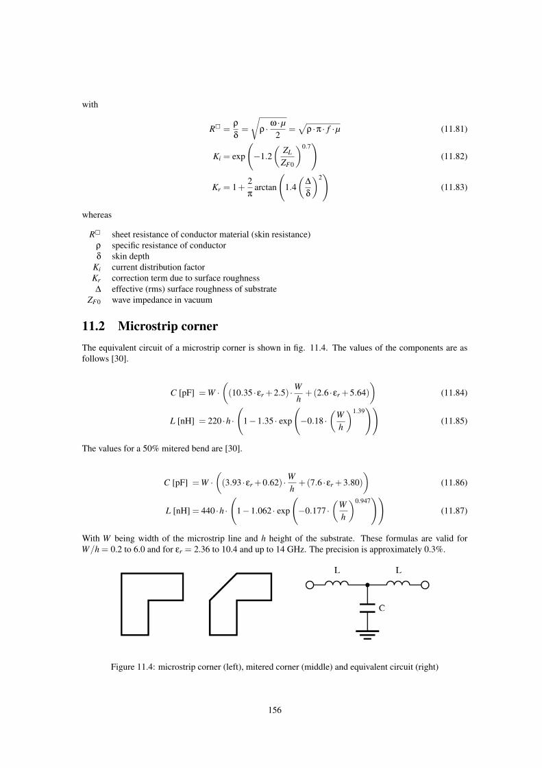
with
R =ρ
δ=√
ρ · ω ·µ2
=√
ρ ·π · f ·µ (11.81)
Ki = exp
(−1.2
(ZL
ZF0
)0.7)
(11.82)
Kr = 1+2π
arctan
(1.4(
∆
δ
)2)
(11.83)
whereas
R sheet resistance of conductor material (skin resistance)ρ specific resistance of conductorδ skin depth
Ki current distribution factorKr correction term due to surface roughness∆ effective (rms) surface roughness of substrate
ZF0 wave impedance in vacuum
11.2 Microstrip cornerThe equivalent circuit of a microstrip corner is shown in fig. 11.4. The values of the components are asfollows [30].
C [pF] = W ·(
(10.35 ·εr +2.5) ·Wh
+(2.6 ·εr +5.64))
(11.84)
L [nH] = 220 ·h ·
(1−1.35 · exp
(−0.18 ·
(Wh
)1.39))
(11.85)
The values for a 50% mitered bend are [30].
C [pF] = W ·(
(3.93 ·εr +0.62) ·Wh
+(7.6 ·εr +3.80))
(11.86)
L [nH] = 440 ·h ·
(1−1.062 · exp
(−0.177 ·
(Wh
)0.947))
(11.87)
With W being width of the microstrip line and h height of the substrate. These formulas are valid forW/h = 0.2 to 6.0 and for εr = 2.36 to 10.4 and up to 14 GHz. The precision is approximately 0.3%.
Figure 11.4: microstrip corner (left), mitered corner (middle) and equivalent circuit (right)
156
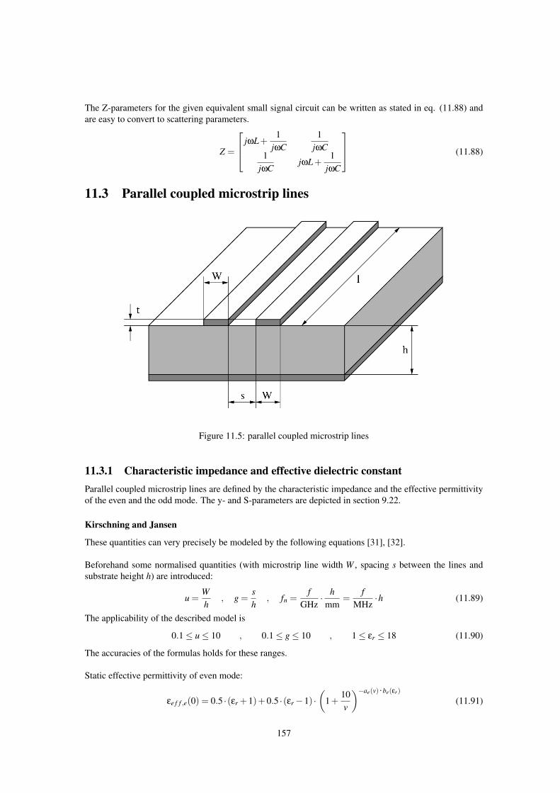
The Z-parameters for the given equivalent small signal circuit can be written as stated in eq. (11.88) andare easy to convert to scattering parameters.
Z =
jωL+1
jωC1
jωC1
jωCjωL+
1jωC
(11.88)
11.3 Parallel coupled microstrip lines
Figure 11.5: parallel coupled microstrip lines
11.3.1 Characteristic impedance and effective dielectric constantParallel coupled microstrip lines are defined by the characteristic impedance and the effective permittivityof the even and the odd mode. The y- and S-parameters are depicted in section 9.22.
Kirschning and Jansen
These quantities can very precisely be modeled by the following equations [31], [32].
Beforehand some normalised quantities (with microstrip line width W , spacing s between the lines andsubstrate height h) are introduced:
u =Wh
, g =sh
, fn =f
GHz· h
mm=
fMHz
·h (11.89)
The applicability of the described model is
0.1≤ u≤ 10 , 0.1≤ g≤ 10 , 1≤ εr ≤ 18 (11.90)
The accuracies of the formulas holds for these ranges.
Static effective permittivity of even mode:
εe f f ,e(0) = 0.5 ·(εr +1)+0.5 ·(εr−1) ·(
1+10v
)−ae(v)·be(εr)
(11.91)
157
with
v = u · 20+g2
10+g2 +g · exp(−g) (11.92)
ae (v) = 1+149· ln
(v4 +(v/52)2
v4 +0.432
)+
118.7
· ln(
1+( v
18.1
)3)
(11.93)
be (εr) = 0.564 ·(
εr−0.9εr +3
)0.053
(11.94)
Static effective permittivity of odd mode:
εe f f ,o(0) = (0.5 · (εr +1)+ao (u,εr)− εe f f (0)) · exp(−co ·gdo
)+ εe f f (0) (11.95)
with
ao (u,εr) = 0.7287 · (εe f f (0)−0.5 · (εr +1)) · (1− exp(−0.179 ·u)) (11.96)
bo (εr) = 0.747 · εr
0.15+ εr(11.97)
co = bo(εr)− (bo (εr)−0.207) · exp(−0.414 ·u) (11.98)do = 0.593+0.694 · exp(−0.562 ·u) (11.99)
whence εe f f (0) refers to the zero-thickness single microstrip line of width W according to [18] (see alsoeq. (11.15)).
The dispersion formulae for the odd and even mode write as follows.
εe f f ,e,o ( fn) = εr−εr− εe f f ,e,o(0)
1+Fe,o ( fn)(11.100)
The frequency dependence for the even mode is
Fe ( fn) = P1 ·P2 · ((P3 ·P4 +0.1844 ·P7) · fn)1.5763 (11.101)
with
P1 = 0.27488+(
0.6315+0.525
(1+0.0157 · fn)20
)·u−0.065683 · exp(−8.7513 ·u) (11.102)
P2 = 0.33622 · (1− exp(−0.03442 ·εr)) (11.103)
P3 = 0.0363 · exp(−4.6 ·u) ·(
1− exp(−( fn/38.7)4.97
))(11.104)
P4 = 1+2.751 ·(
1− exp(−(εr/15.916)8
))(11.105)
P5 = 0.334 · exp(−3.3 · (εr/15)3
)+0.746 (11.106)
P6 = P5 · exp(−( fn/18)0.368
)(11.107)
P7 = 1+4.069 ·P6 ·g0.479 · exp(−1.347 ·g0.595−0.17 ·g2.5
)(11.108)
The frequency dependence for the odd mode is
Fo ( fn) = P1 ·P2 · ((P3 ·P4 +0.1844) · fn ·P15)1.5763 (11.109)
158
with
P8 = 0.7168 ·(
1+1.076
1+0.0576 · (εr−1)
)(11.110)
P9 = P8−0.7913 ·(
1− exp(−( fn/20)1.424
))· arctan
(2.481 · (εr/8)0.946
)(11.111)
P10 = 0.242 · (εr−1)0.55 (11.112)
P11 = 0.6366 · (exp(−0.3401 · fn)−1) · arctan(
1.263 · (u/3)1.629)
(11.113)
P12 = P9 +1−P9
1+1.183 ·u1.376 (11.114)
P13 = 1.695 · P10
0.414+1.605 ·P10(11.115)
P14 = 0.8928+0.1072 ·(
1− exp(−0.42 · ( fn/20)3.215
))(11.116)
P15 =∣∣1−0.8928 · (1+P11) · exp
(−P13 ·g1.092) ·P12/P14
∣∣ (11.117)
Up to fn = 25 the maximum error of these equations is 1.4%.
The static characteristic impedance for the even mode writes as follows.
ZL,e(0) =
√εe f f (0)
εe f f ,e(0)· ZL(0)
1− ZL(0)377Ω
·√
εe f f (0) ·Q4
(11.118)
with
Q1 = 0.8695 ·u0.194 (11.119)
Q2 = 1+0.7519 ·g+0.189 ·g2.31 (11.120)
Q3 = 0.1975+(
16.6+(8.4/g)6)−0.387
+1
241· ln
(g10
1+(g/3.4)10
)(11.121)
Q4 =Q1
Q2· 2
exp(−g) ·uQ3 +(2− exp(−g)) ·u−Q3(11.122)
with ZL(0) and εe f f (0) being again quantities for a zero-thickness single microstrip line of width W ac-cording to [18] (see also eq. (11.15) and (11.5)).
The static characteristic impedance for the odd mode writes as follows.
ZL,o(0) =
√εe f f (0)
εe f f ,o(0)· ZL(0)
1− ZL(0)377Ω
·√
εe f f (0) ·Q10
(11.123)
159
with
Q5 = 1.794+1.14 · ln(
1+0.638
g+0.517 ·g2.43
)(11.124)
Q6 = 0.2305+1
281.3· ln
(g10
1+(g/5.8)10
)+
15.1· ln(
1+0.598 ·g1.154)
(11.125)
Q7 =10+190 ·g2
1+82.3 ·g3 (11.126)
Q8 = exp(−6.5−0.95 · ln(g)− (g/0.15)5
)(11.127)
Q9 = ln(Q7) · (Q8 +1/16.5) (11.128)
Q10 =Q2 ·Q4−Q5 · exp
(ln(u) ·Q6 ·u−Q9
)Q2
= Q4−Q5
Q2·uQ6 ·u−Q9 (11.129)
The accuracy of the static impedances is better than 0.6%.
Dispersion of the characteristic impedance for the even mode can be modeled by the following equations.
ZL,e( fn) = ZL,e(0) ·
(0.9408 ·(εe f f ( fn))Ce −0.9603
(0.9408−de) · (εe f f (0))Ce −0.9603
)Q0
(11.130)
with
Ce = 1+1.275 ·(
1− exp(−0.004625 · pe ·ε1.674
r · ( fn/18.365)2.745))
−Q12 +Q16−Q17 +Q18 +Q20
(11.131)
de = 5.086 ·qe ·re
0.3838+0.386 ·qe·
exp(−22.2 ·u1.92
)1+1.2992 ·re
· (εr−1)6
1+10 ·(εr−1)6 (11.132)
pe = 4.766 · exp(−3.228 ·u0.641
)(11.133)
qe = 0.016+(0.0514 ·εr ·Q21)4.524 (11.134)
re = ( fn/28.843)12 (11.135)
160
and
Q11 = 0.893 ·(
1− 0.31+0.7 · (εr−1)
)(11.136)
Q12 = 2.121 · ( fn/20)4.91
1+Q11 · ( fn/20)4.91 · exp(−2.87 ·g) ·g0.902 (11.137)
Q13 = 1+0.038 · (εr/8)5.1 (11.138)
Q14 = 1+1.203 · (εr/15)4
1+ · (εr/15)4 (11.139)
Q15 =1.887 · exp
(−1.5 ·g0.84
)·gQ14
1+0.41 · ( fn/15)3 · u2/Q13
0.125+u1.626/Q13
(11.140)
Q16 = Q15 ·
(1+
9
1+0.403 · (εr−1)2
)(11.141)
Q17 = 0.394 ·(
1− exp(−1.47 · (u/7)0.672
))·(
1− exp(−4.25( fn/20)1.87
))(11.142)
Q18 = 0.61 ·1− exp
(−2.13 · (u/8)1.593
)1+6.544 ·g4.17 (11.143)
Q19 =0.21 ·g4
(1+0.18 ·g4.9) · (1+0.1 ·u2) ·(
1+( fn/24)3) (11.144)
Q20 = Q19 ·
(0.09+
1
1+0.1 · (εr−1)2.7
)(11.145)
Q21 =∣∣∣∣1−42.54 ·g0.133 · exp(−0.812 ·g) · u2.5
1+0.033 ·u2.5
∣∣∣∣ (11.146)
With εe f f ( fn) being the single microstrip effective dielectric constant according to [20] (see eq. (11.26))and Q0 single microstrip impedance dispersion according to [21] (there denoted as R17, see eq. (11.49)).
Dispersion of the characteristic impedance for the odd mode can be modeled by the following equations.
ZL,o( fn) = ZL( fn)+ZL,o(0) ·
(εe f f ,o( fn)εe f f ,o(0)
)Q22
−ZL( fn) ·Q23
1+Q24 +(0.46 ·g)2.2 ·Q25(11.147)
161
with
Q22 = 0.925 · ( fn/Q26)1.536
1+0.3 · ( fn/30)1.536 (11.148)
Q23 = 1+0.005 · fn ·Q27(
1+0.812 · ( fn/15)1.9)· (1+0.025 ·u2)
(11.149)
Q24 =2.506 ·Q28 ·u0.894
3.575+u0.894 ·(
(1+1.3 ·u) · fn
99.25
)4.29
(11.150)
Q25 =0.3 · f 2
n
10+ f 2n·
(1+
2.333 · (εr−1)2
5+(εr−1)2
)(11.151)
Q26 = 30−22.2 ·
(εr−1
13
)12
1+3 ·(
εr−113
)12 −Q29 (11.152)
Q27 = 0.4 ·g0.84 ·
(1+
2.5 · (εr−1)1.5
5+(εr−1)1.5
)(11.153)
Q28 = 0.149 · (εr−1)3
94.5+0.038 · (εr−1)3 (11.154)
Q29 =15.16
1+0.196 · (εr−1)2 (11.155)
with ZL( fn) being the frequency-dependent power-current characteristic impedance formulation of a singlemicrostrip with width W according to [21] (see eq. (11.50)). Up to fn = 20, the numerical error of ZL,o( fn)and ZL,e( fn) is less than 2.5%.
Hammerstad and Jensen
The equations given by E. Hammerstad and Ø. Jensen [18] represent the first generally valid model ofcoupled microstrips with an acceptable accuracy. The model equations have been validated in the range0.1≤ u≤ 10 and g≥ 0.01, a range which should cover that used in practice.
The homogeneous mode impedances are
ZL,e,o (u,g) =ZL(u)
1−ZL(u) ·Φe,o (u,g)/ZF0(11.156)
The effective dielectric constants are
εe f f ,e,o (u,g,εr) =εr +1
2+
εr−12·Fe,o (u,g,εr) (11.157)
with
Fe (u,g,εr) =(
1+10
µ(u,g)
)−a(µ)·b(εr)
(11.158)
Fo (u,g,εr) = fo (u,g,εr) ·(
1+10u
)−a(u)·b(εr)
(11.159)
whence a(u) and b(εr) denote eqs. (11.16) and (11.17) of the single microstrip line. The characteristicimpedance of the single microstrip line ZL (u) also defined in [18] is given by eq. (11.5). The modifying
162
equations for the even mode are as follows
Φe (u,g) =ϕ(u)
Ψ(g) ·(α(g) ·um(g) +(1−α(g)) ·u−m(g)
) (11.160)
ϕ(u) = 0.8645 ·u0.172 (11.161)
Ψ(g) = 1+g
1.45+
g2.09
3.95(11.162)
α(g) = 0.5 ·e−g (11.163)
m(g) = 0.2175+(
4.113+(20.36/g)6)−0.251
+1
323· ln
(g10
1+(g/13.8)10
)(11.164)
The modifying equations for the odd mode are as follows
Φo (u,g) = Φe (u,g)− θ(g)Ψ(g)
· exp(
β(g) ·u−n(g) · lnu)
(11.165)
θ(g) = 1.729+1.175 · ln(
1+0.627
g+0.327 ·g2.17
)(11.166)
β(g) = 0.2306+1
301.8· ln
(g10
1+(g/3.73)10
)+
15.3· ln(
1+0.646 ·g1.175)
(11.167)
n(g) =(
117.7
+ exp(−6.424−0.76 · lng− (g/0.23)5
))· ln(
10+68.3 ·g2
1+32.5 ·g3.093
)(11.168)
Furthermore
µ(u,g) = g ·e−g +u · 20+g2
10+g2 (11.169)
fo (u,g,εr) = fo1 (g,εr) · exp(p(g) · lnu+q(g) · sin(π · logu)) (11.170)
p(g) =exp(−0.745 ·g0.295
)cosh(g0.68)
(11.171)
q(g) = exp(−1.366−g) (11.172)
fo1 (g,εr) = 1− exp
−0.179 ·g0.15− 0.328 ·gr(g,εr)
ln(
e+(g/7)2.8) (11.173)
r (g,εr) = 1+0.15 ·
1−exp(
1− (εr−1)2 /8.2)
1+g−6
(11.174)
The quasi-static characteristic impedance ZL(u) of a zero-thickness single microstrip line denoted in eq.(11.156) can either be calculated using the below equations with εre f f being the quasi-static effective di-electric constant defined by eq. (11.15) or using eqs. (11.5) and (11.15).
ZL1(u) =ZF0
u+1.98 ·u0.172 (11.175)
ZL(u) =ZL1(u)√
εre f f
(11.176)
The errors in the even and odd mode impedances ZL,e and ZL,e were found to be less than 0.8% and lessthan 0.3% for the wavelengths.
The model does not include the effect of non-zero strip thickness or asymmetry. Dispersion is also notincluded. W. J. Getsinger [33] has proposed modifications to his single strip dispersion model, but unfor-tunately it is easily shown that the results are asymptotically wrong for extreme values of gap width.
163
In fact he correctly assumes that in the even mode the two strips are at the same potential, and the totalcurrent is twice that on a single strip, and dispersion for even-mode propagation is computed by substitutingZL,e/2 for ZL in eqs. (11.60) and (11.61). In the odd mode the two strips are at opposite potentials, and thevoltage between strips is twice that of a single strip to ground. Thus the total mode impedance is twice thatof a single strip, and the dispersion for odd-mode propagation is computed substituting 2ZL,o for ZL in eqs.(11.60) and (11.61).
εr,e,o ( f ) = εr−εr− εre f f ,e,o
1+G ·(
ffp
)2 (11.177)
with
fp =
ZL,e
4µ0heven mode
ZL,o
µ0hodd mode
(11.178)
G =
0.6+ZL,e ·0.0045 even mode
0.6+ZL,o ·0.018 odd mode(11.179)
11.3.2 Strip thickness correctionAccording to R.H. Jansen [34] corrected strip width values have been found in the range of technologicallymeaningful geometries to be
Wt,e = W +∆W ·(
1−0.5 · exp(−0.69 · ∆W
∆t
))(11.180)
Wt,o = Wt,e +∆t (11.181)
with∆t =
2 · t ·hs ·εr
for s 2t (11.182)
The author refers to the modifications of the strip width of a single microstrip line ∆W given by Hammerstadand Bekkadal. See also eq. (11.21) on page 150.
∆W =
tπ·(
1+ ln(
2ht
))for W >
h2π
> 2t
tπ·(
1+ ln(
4πWt
))for
h2π≥W > 2t
(11.183)
For large spacings s the single line formulae (11.183) applies.
11.3.3 Transmission lossesThe loss equations given by E. Hammerstad and Ø. Jensen [18] for the single microstrip line are also validfor coupled microstrips, provided that the dielectric filling factor, homogeneous impedance, and currentdistribution factor of the actual mode are used. The following approximation gives good results for oddand even current distribution factors (modification of eq. (11.82)).
Ki,e = Ki,o = exp
(−1.2 ·
(ZL,e +ZL,o
2 ·ZF0
)0.7)
(11.184)
164
11.4 Microstrip openA microstrip open end can be modeled by a longer effective microstrip line length ∆l as described by M.Kirschning, R.H. Jansen and N.H.L. Koster [35].
∆lh
=Q1 ·Q3 ·Q5
Q4(11.185)
with
Q1 = 0.434907 ·ε0.81
r,e f f +0.26
ε0.81r,e f f −0.189
· (W/h)0.8544 +0.236
(W/h)0.8544 +0.87(11.186)
Q2 = 1+(W/h)0.371
2.358 ·εr +1(11.187)
Q3 = 1+0.5274ε
0.9236r,e f f
· arctan(
0.084 · (W/h)1.9413
Q2
)(11.188)
Q4 = 1+0.0377 · (6−5 · exp(0.036 · (1− εr))) · arctan(
0.067 · (W/h)1.456)
(11.189)
Q5 = 1−0.218 · exp(−7.5 ·W/h) (11.190)
The numerical error is less than 2.5% for 0.01≤W/h≤ 100 and 1≤ εr ≤ 50.
Another microstrip open end model was published by E. Hammerstad [36]:
∆lh
= 0.102 ·W/h+0.106W/h+0.264
·(
1.166+εr +1
εr· (0.9+ ln(W/h+2.475))
)(11.191)
Here the numerical error is less than 1.7% for W/h < 20.
In order to simplify calculations, the equivalent additional line length ∆l can be transformed into an equiv-alent open end capacitance Cend :
Cend = C′ ·∆l =√
εr,e f f
c0 ·ZL∆l (11.192)
With C′ being the capacitance per length and c0 = 299 792 458 m/s being the vacuum light velocity.
11.5 Microstrip gapA symmetrical microstrip gap can be modeled by two open ends with a capacitive series coupling betweenthe two ends. The physical layout is shown in fig. 11.6.
165
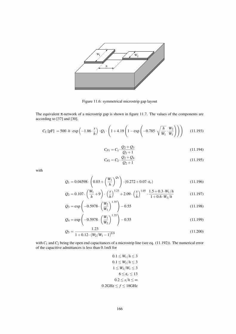
Figure 11.6: symmetrical microstrip gap layout
The equivalent π-network of a microstrip gap is shown in figure 11.7. The values of the components areaccording to [37] and [30].
CS [pF] = 500 ·h · exp(−1.86 · s
h
)·Q1 ·
(1+4.19
(1− exp
(−0.785 ·
√h
W1·W2
W1
)))(11.193)
CP1 = C1 ·Q2 +Q3
Q2 +1(11.194)
CP2 = C2 ·Q2 +Q4
Q2 +1(11.195)
with
Q1 = 0.04598 ·
(0.03+
(W1
h
)Q5)·(0.272+0.07 ·εr) (11.196)
Q2 = 0.107 ·(
W1
h+9)·( s
h
)3.23+2.09 ·
( sh
)1.05· 1.5+0.3 ·W1/h
1+0.6 ·W1/h(11.197)
Q3 = exp
(−0.5978 ·
(W2
W1
)1.35)−0.55 (11.198)
Q4 = exp
(−0.5978 ·
(W1
W2
)1.35)−0.55 (11.199)
Q5 =1.23
1+0.12 · (W2/W1−1)0.9 (11.200)
with C1 and C2 being the open end capacitances of a microstrip line (see eq. (11.192)). The numerical errorof the capacitive admittances is less than 0.1mS for
0.1≤W1/h≤ 30.1≤W2/h≤ 31≤W2/W1 ≤ 3
6≤ εr ≤ 130.2≤ s/h≤ ∞
0.2GHz≤ f ≤ 18GHz
166
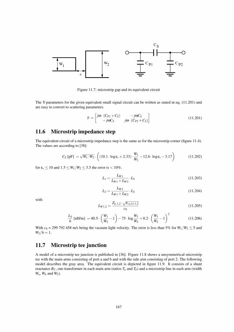
Figure 11.7: microstrip gap and its equivalent circuit
The Y-parameters for the given equivalent small signal circuit can be written as stated in eq. (11.201) andare easy to convert to scattering parameters.
Y =[
jω · (CP1 +CS) − jωCS− jωCS jω · (CP2 +CS)
](11.201)
11.6 Microstrip impedance stepThe equivalent circuit of a microstrip impedance step is the same as for the microstrip corner (figure 11.4).The values are according to [38]:
CS [pF] =√
W1 ·W2 ·(
(10.1 · logεr +2.33) ·W1
W2−12.6 · logεr−3.17
)(11.202)
for εr ≤ 10 and 1.5≤W1/W2 ≤ 3.5 the error is < 10%.
L1 =LW1
LW1 +LW2·LS (11.203)
L2 =LW2
LW1 +LW2·LS (11.204)
with
LW1,2 =ZL,1,2 ·
√εr,e f f ,1,2
c0(11.205)
LS
h[nH/m] = 40.5 ·
(W1
W2−1)−75 · log
W1
W2+0.2 ·
(W1
W2−1)2
(11.206)
With c0 = 299 792 458 m/s being the vacuum light velocity. The error is less than 5% for W1/W2 ≤ 5 andW2/h = 1.
11.7 Microstrip tee junctionA model of a microstrip tee junction is published in [36]. Figure 11.8 shows a unsymmetrical microstriptee with the main arms consisting of port a and b and with the side arm consisting of port 2. The followingmodel describes the gray area. The equivalent circuit is depicted in figure 11.9. It consists of a shuntreactance BT , one transformer in each main arm (ratios Ta and Tb) and a microstrip line in each arm (widthWa, Wb and W2).
167
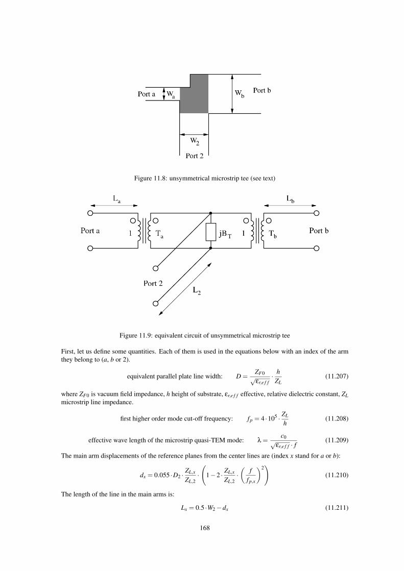
Figure 11.8: unsymmetrical microstrip tee (see text)
Figure 11.9: equivalent circuit of unsymmetrical microstrip tee
First, let us define some quantities. Each of them is used in the equations below with an index of the armthey belong to (a, b or 2).
equivalent parallel plate line width: D =ZF0√εr,e f f
· hZL
(11.207)
where ZF0 is vacuum field impedance, h height of substrate, εr,e f f effective, relative dielectric constant, ZLmicrostrip line impedance.
first higher order mode cut-off frequency: fp = 4 ·105 · ZL
h(11.208)
effective wave length of the microstrip quasi-TEM mode: λ =c0√
εr,e f f · f(11.209)
The main arm displacements of the reference planes from the center lines are (index x stand for a or b):
dx = 0.055 ·D2 ·ZL,x
ZL,2·
(1−2 ·
ZL,x
ZL,2·(
ffp,x
)2)
(11.210)
The length of the line in the main arms is:
Lx = 0.5 ·W2−dx (11.211)
168
where f is frequency.
The side arm displacement of the reference planes from the center lines is:
d2 =√
Da ·Db · (0.5−R · (0.05+0.7 · exp(−1.6 ·R)+0.25 ·R ·Q−0.17 · lnR)) (11.212)
The length of the line in the side arm is:
L2 = 0.5 ·max(Wa,Wb)−d2 (11.213)
where max(x,y) is the larger of the both quantities, R and Q are:
R =
√ZL,a ·ZL,b
ZL,2Q =
f 2
fp,a · fp,b(11.214)
Turn ratio of transformers in the side arms:
T 2x = 1−π ·
(f
fp,x
)2
·
(1
12·(
ZL,x
ZL,2
)2
+(
0.5− d2
Dx
)2)
(11.215)
Shunt susceptance:
BT = 5.5 ·√
Da ·Db
λa ·λb· εr +2
εr· 1
ZL,2 ·Ta ·Tb·√
da ·db
D2
·
(1+0.9 · lnR+4.5 ·R ·Q−4.4 · exp(−1.3 ·R)−20 ·
(ZL,2
ZF0
)2) (11.216)
For better implementation of the microstrip tee (figure 11.9) the device parameter of the internal equivalentcircuit (two transformers and the shunt susceptance) are given below. The port numbering for them is porta = 1, port b = 2 and port 2 = 3.
(Y ) = infinity (11.217)
(Z) =1
j ·BT·
1n2
a
1na ·nb
1na
1na ·nb
1n2
b
1nb
1na
1nb
1
(11.218)
S11 =1−n2
a ·( j ·BT ·Z0 + 1n2
b+1)
1+n2a ·( j ·BT ·Z0 + 1
n2b+1)
(11.219)
S22 =1−n2
b ·( j ·BT ·Z0 + 1n2
a+1)
1+n2b ·( j ·BT ·Z0 + 1
n2a+1)
(11.220)
S33 =1−(
1n2
a+ 1
n2b+ j ·BT ·Z0
)1+(
1n2
a+ 1
n2b+ j ·BT ·Z0
) (11.221)
S13 = S31 =2 ·na
n2a ·(
1n2
b+ j ·BT ·Z0 +1
)+1
(11.222)
S23 = S32 =2 ·nb
n2b ·(
1n2
a+ j ·BT ·Z0 +1
)+1
(11.223)
169
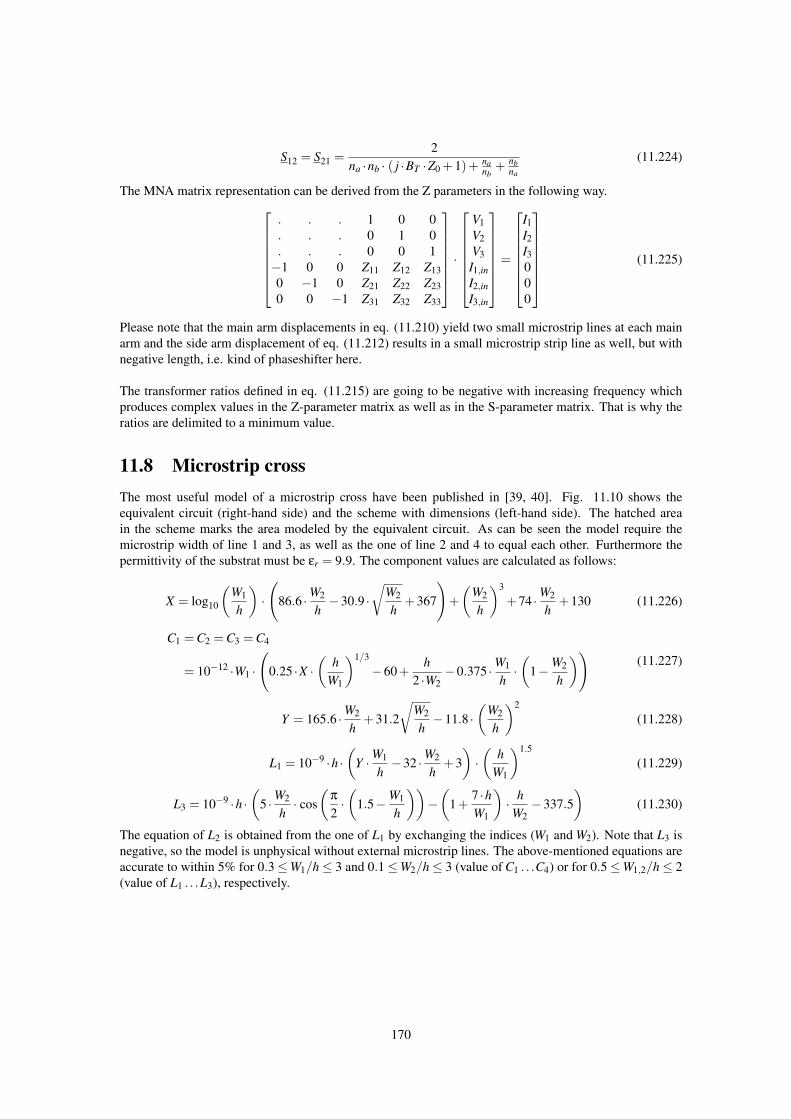
S12 = S21 =2
na ·nb · ( j ·BT ·Z0 +1)+ nanb
+ nbna
(11.224)
The MNA matrix representation can be derived from the Z parameters in the following way.. . . 1 0 0. . . 0 1 0. . . 0 0 1−1 0 0 Z11 Z12 Z130 −1 0 Z21 Z22 Z230 0 −1 Z31 Z32 Z33
·
V1V2V3I1,inI2,inI3,in
=
I1I2I3000
(11.225)
Please note that the main arm displacements in eq. (11.210) yield two small microstrip lines at each mainarm and the side arm displacement of eq. (11.212) results in a small microstrip strip line as well, but withnegative length, i.e. kind of phaseshifter here.
The transformer ratios defined in eq. (11.215) are going to be negative with increasing frequency whichproduces complex values in the Z-parameter matrix as well as in the S-parameter matrix. That is why theratios are delimited to a minimum value.
11.8 Microstrip crossThe most useful model of a microstrip cross have been published in [39, 40]. Fig. 11.10 shows theequivalent circuit (right-hand side) and the scheme with dimensions (left-hand side). The hatched areain the scheme marks the area modeled by the equivalent circuit. As can be seen the model require themicrostrip width of line 1 and 3, as well as the one of line 2 and 4 to equal each other. Furthermore thepermittivity of the substrat must be εr = 9.9. The component values are calculated as follows:
X = log10
(W1
h
)·
(86.6 ·W2
h−30.9 ·
√W2
h+367
)+(
W2
h
)3
+74 ·W2
h+130 (11.226)
C1 = C2 = C3 = C4
= 10−12 ·W1 ·
(0.25 ·X ·
(h
W1
)1/3
−60+h
2 ·W2−0.375 ·W1
h·(
1−W2
h
))(11.227)
Y = 165.6 ·W2
h+31.2
√W2
h−11.8 ·
(W2
h
)2
(11.228)
L1 = 10−9 ·h ·(
Y ·W1
h−32 ·W2
h+3)·(
hW1
)1.5
(11.229)
L3 = 10−9 ·h ·(
5 ·W2
h· cos
(π
2·(
1.5−W1
h
))−(
1+7 ·hW1
)· hW2−337.5
)(11.230)
The equation of L2 is obtained from the one of L1 by exchanging the indices (W1 and W2). Note that L3 isnegative, so the model is unphysical without external microstrip lines. The above-mentioned equations areaccurate to within 5% for 0.3≤W1/h≤ 3 and 0.1≤W2/h≤ 3 (value of C1 . . .C4) or for 0.5≤W1,2/h≤ 2(value of L1 . . .L3), respectively.
170
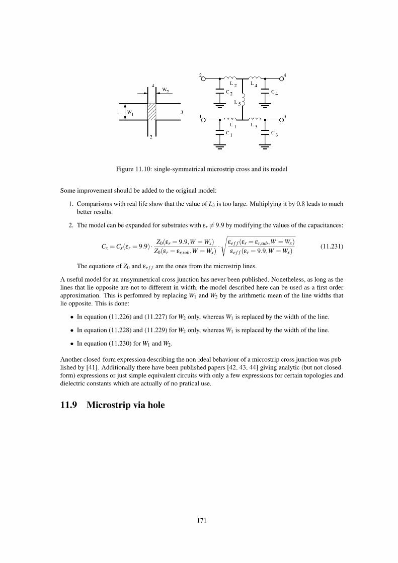
Figure 11.10: single-symmetrical microstrip cross and its model
Some improvement should be added to the original model:
1. Comparisons with real life show that the value of L3 is too large. Multiplying it by 0.8 leads to muchbetter results.
2. The model can be expanded for substrates with εr 6= 9.9 by modifying the values of the capacitances:
Cx = Cx(εr = 9.9) · Z0(εr = 9.9,W = Wx)Z0(εr = εr,sub,W = Wx)
·
√εe f f (εr = εr,sub,W = Wx)εe f f (εr = 9.9,W = Wx)
(11.231)
The equations of Z0 and εe f f are the ones from the microstrip lines.
A useful model for an unsymmetrical cross junction has never been published. Nonetheless, as long as thelines that lie opposite are not to different in width, the model described here can be used as a first orderapproximation. This is perfomred by replacing W1 and W2 by the arithmetic mean of the line widths thatlie opposite. This is done:
• In equation (11.226) and (11.227) for W2 only, whereas W1 is replaced by the width of the line.
• In equation (11.228) and (11.229) for W2 only, whereas W1 is replaced by the width of the line.
• In equation (11.230) for W1 and W2.
Another closed-form expression describing the non-ideal behaviour of a microstrip cross junction was pub-lished by [41]. Additionally there have been published papers [42, 43, 44] giving analytic (but not closed-form) expressions or just simple equivalent circuits with only a few expressions for certain topologies anddielectric constants which are actually of no pratical use.
11.9 Microstrip via hole
171
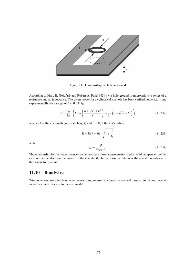
Figure 11.11: microstrip via hole to ground
According to Marc E. Goldfarb and Robert A. Pucel [45] a via hole ground in microstrip is a series of aresistance and an inductance. The given model for a cylindrical via hole has been verified numerically andexperimentally for a range of h < 0.03 ·λ0.
L =µ0
2π·
(h · ln
(h+√
r2 +h2
r
)+
32·(
r−√
r2 +h2))
(11.232)
whence h is the via length (substrate height) and r = D/2 the via’s radius.
R = R( f = 0) ·
√1+
ffδ
(11.233)
withfδ =
ρ
π ·µ0 · t2 (11.234)
The relationship for the via resistance can be used as a close approximation and is valid independent of theratio of the metalization thickness t to the skin depth. In the formula ρ denotes the specific resistance ofthe conductor material.
11.10 BondwireWire inductors, so called bond wire connections, are used to connect active and passive circuit componentsas well as micro devices to the real world.
172
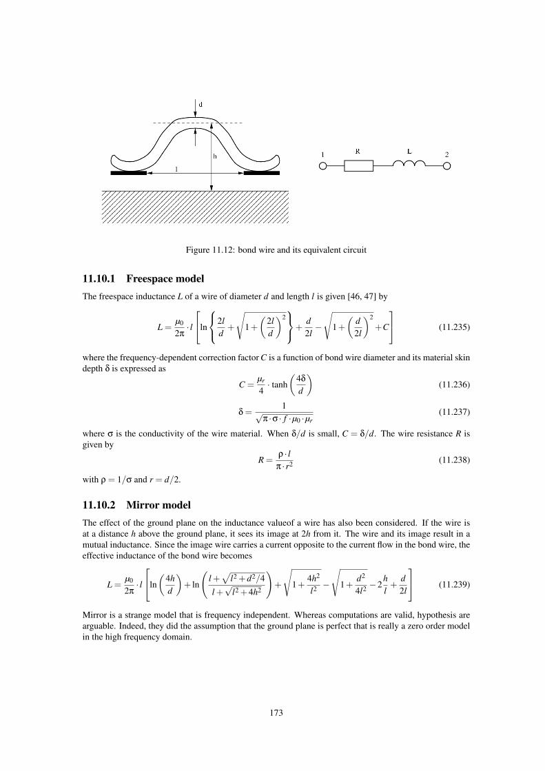
Figure 11.12: bond wire and its equivalent circuit
11.10.1 Freespace modelThe freespace inductance L of a wire of diameter d and length l is given [46, 47] by
L =µ0
2π· l
ln
2ld
+
√1+(
2ld
)2+
d2l−
√1+(
d2l
)2
+C
(11.235)
where the frequency-dependent correction factor C is a function of bond wire diameter and its material skindepth δ is expressed as
C =µr
4· tanh
(4δ
d
)(11.236)
δ =1√
π ·σ · f ·µ0 ·µr(11.237)
where σ is the conductivity of the wire material. When δ/d is small, C = δ/d. The wire resistance R isgiven by
R =ρ · l
π ·r2 (11.238)
with ρ = 1/σ and r = d/2.
11.10.2 Mirror modelThe effect of the ground plane on the inductance valueof a wire has also been considered. If the wire isat a distance h above the ground plane, it sees its image at 2h from it. The wire and its image result in amutual inductance. Since the image wire carries a current opposite to the current flow in the bond wire, theeffective inductance of the bond wire becomes
L =µ0
2π· l
ln(
4hd
)+ ln
(l +√
l2 +d2/4l +√
l2 +4h2
)+
√1+
4h2
l2 −
√1+
d2
4l2 −2hl
+d2l
(11.239)
Mirror is a strange model that is frequency independent. Whereas computations are valid, hypothesis arearguable. Indeed, they did the assumption that the ground plane is perfect that is really a zero order modelin the high frequency domain.
173
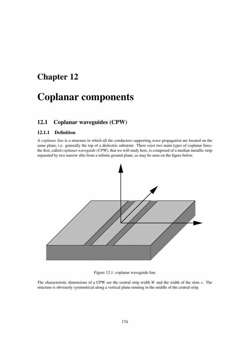
Chapter 12
Coplanar components
12.1 Coplanar waveguides (CPW)
12.1.1 DefinitionA coplanar line is a structure in which all the conductors supporting wave propagation are located on thesame plane, i.e. generally the top of a dielectric substrate. There exist two main types of coplanar lines:the first, called coplanar waveguide (CPW), that we will study here, is composed of a median metallic stripseparated by two narrow slits from a infinite ground plane, as may be seen on the figure below.
Figure 12.1: coplanar waveguide line
The characteristic dimensions of a CPW are the central strip width W and the width of the slots s. Thestructure is obviously symmetrical along a vertical plane running in the middle of the central strip.
174
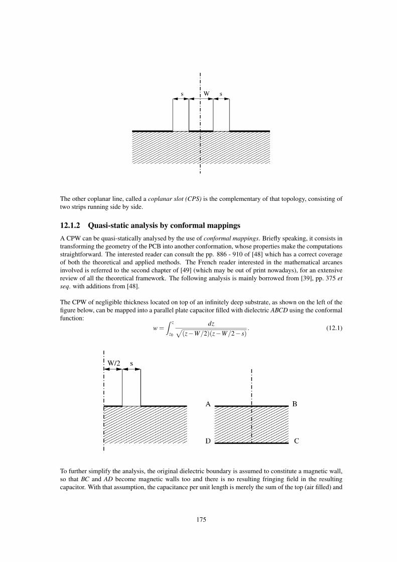
The other coplanar line, called a coplanar slot (CPS) is the complementary of that topology, consisting oftwo strips running side by side.
12.1.2 Quasi-static analysis by conformal mappingsA CPW can be quasi-statically analysed by the use of conformal mappings. Briefly speaking, it consists intransforming the geometry of the PCB into another conformation, whose properties make the computationsstraightforward. The interested reader can consult the pp. 886 - 910 of [48] which has a correct coverageof both the theoretical and applied methods. The French reader interested in the mathematical arcanesinvolved is referred to the second chapter of [49] (which may be out of print nowadays), for an extensivereview of all the theoretical framework. The following analysis is mainly borrowed from [39], pp. 375 etseq. with additions from [48].
The CPW of negligible thickness located on top of an infinitely deep substrate, as shown on the left of thefigure below, can be mapped into a parallel plate capacitor filled with dielectric ABCD using the conformalfunction:
w =Z z
z0
dz√(z−W/2)(z−W/2− s)
. (12.1)
To further simplify the analysis, the original dielectric boundary is assumed to constitute a magnetic wall,so that BC and AD become magnetic walls too and there is no resulting fringing field in the resultingcapacitor. With that assumption, the capacitance per unit length is merely the sum of the top (air filled) and
175
bottom (dielectric filled) partial capacitances. The latter is given by:
Cd = 2 ·ε0 ·εr ·K(k1)K′(k1)
(12.2)
while the former is:
Ca = 2 ·ε0 ·K(k1)K′(k1)
(12.3)
In both formulae K(k) and K′(k) represent the complete elliptic integral of the first kind and its complement,and k1 = W
W+2s . While the separate evaluation of K and K′ is more or less tricky, the K/K′ ratio lets itselfcompute efficiently through the following formulae:
K(k)K′(k)
=π
ln(
2 1+√
k′
1−√
k′
) for 0≤ k ≤ 1√2
(12.4)
K(k)K′(k)
=ln(
2 1+√
k1−√
k
)π
for1√2≤ k ≤ 1 (12.5)
with k′ being the complementary modulus: k′ =√
1− k2. While [48] states that the accuracy of the aboveformulae is close to 10−5, [39] claims it to be 3 ·10−6. It can be considered as exact for any practicalpurposes.
The total line capacitance is thus the sum of Cd and Ca. The effective permittivity is therefore:
εre =εr +1
2(12.6)
and the impedance:
Z =30π√
εre· K′(k1)
K(k1)(12.7)
176
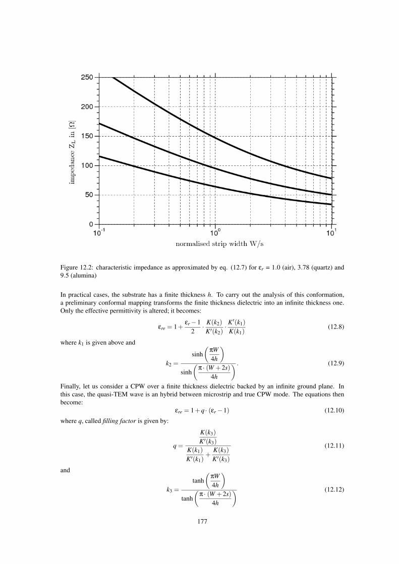
Figure 12.2: characteristic impedance as approximated by eq. (12.7) for εr = 1.0 (air), 3.78 (quartz) and9.5 (alumina)
In practical cases, the substrate has a finite thickness h. To carry out the analysis of this conformation,a preliminary conformal mapping transforms the finite thickness dielectric into an infinite thickness one.Only the effective permittivity is altered; it becomes:
εre = 1+εr−1
2· K(k2)
K′(k2)· K′(k1)
K(k1)(12.8)
where k1 is given above and
k2 =sinh
(πW4h
)sinh
(π · (W +2s)
4h
) . (12.9)
Finally, let us consider a CPW over a finite thickness dielectric backed by an infinite ground plane. Inthis case, the quasi-TEM wave is an hybrid between microstrip and true CPW mode. The equations thenbecome:
εre = 1+q · (εr−1) (12.10)
where q, called filling factor is given by:
q =
K(k3)K′(k3)
K(k1)K′(k1)
+K(k3)K′(k3)
(12.11)
and
k3 =tanh
(πW4h
)tanh
(π · (W +2s)
4h
) (12.12)
177
The impedance of this line amounts to:
Z =60π√
εre· 1
K(k1)K′(k1)
+K(k3)K′(k3)
(12.13)
12.1.3 Effects of metalization thicknessIn most practical cases, the strips are very thin, yet their thickness cannot be entirely neglected. A firstorder correction to take into account the non-zero thickness of the conductor is given by [39]:
se = s−∆ (12.14)
andWe = W +∆ (12.15)
where
∆ =1.25t
π·(
1+ ln(
4πWt
))(12.16)
In the computation of the impedance, both the k1 and the effective dielectric constant are affected, where-fore k1 must be substituted by an “effective” modulus ke, with:
ke =We
We +2se≈ k1 +
(1− k2
1)· ∆
2s(12.17)
and
εtre = εre−
0.7 · (εre−1) · ts
K(k1)K′(k1)
+0.7 · ts
(12.18)
12.1.4 Effects of dispersionThe effects of dispersion in CPW are similar to those encountered in the microstrip lines, though the neteffect on impedance is somewhat different. [39] gives a closed form expression to compute εre( f ) from itsquasi-static value: √
εre( f ) =√
εre(0)+√
εr−√
εre(0)
1+G ·(
ffT E
)−1.8 (12.19)
where:
G = eu· ln(W
s
)+v (12.20)
u = 0.54−0.64p+0.015p2 (12.21)
v = 0.43−0.86p+0.54p2 (12.22)
p = ln(W
h
)(12.23)
and fT E is the cut-off frequency of the T E0 mode, defined by:
fT E =c
4h ·√
εr−1. (12.24)
This dispersion expression was first reported by [50] and has been reused and extended in [51]. Theaccuracy of this expression is claimed to be better than 5% for 0.1≤W/h≤ 5, 0.1≤W/s≤ 5, 1.5≤ εr ≤ 50and 0≤ f / fT E ≤ 10.
178
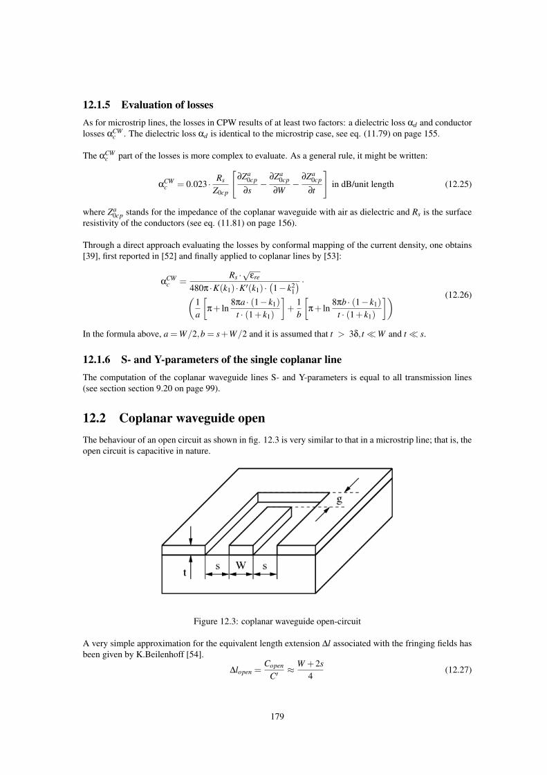
12.1.5 Evaluation of lossesAs for microstrip lines, the losses in CPW results of at least two factors: a dielectric loss αd and conductorlosses αCW
c . The dielectric loss αd is identical to the microstrip case, see eq. (11.79) on page 155.
The αCWc part of the losses is more complex to evaluate. As a general rule, it might be written:
αCWc = 0.023 · Rs
Z0cp
[∂Za
0cp
∂s−
∂Za0cp
∂W−
∂Za0cp
∂t
]in dB/unit length (12.25)
where Za0cp stands for the impedance of the coplanar waveguide with air as dielectric and Rs is the surface
resistivity of the conductors (see eq. (11.81) on page 156).
Through a direct approach evaluating the losses by conformal mapping of the current density, one obtains[39], first reported in [52] and finally applied to coplanar lines by [53]:
αCWc =
Rs ·√
εre
480π ·K(k1) ·K′(k1) ·(1− k2
1
) ·(1a
[π+ ln
8πa · (1− k1)t · (1+ k1)
]+
1b
[π+ ln
8πb · (1− k1)t · (1+ k1)
]) (12.26)
In the formula above, a = W/2,b = s+W/2 and it is assumed that t > 3δ, tW and t s.
12.1.6 S- and Y-parameters of the single coplanar lineThe computation of the coplanar waveguide lines S- and Y-parameters is equal to all transmission lines(see section section 9.20 on page 99).
12.2 Coplanar waveguide openThe behaviour of an open circuit as shown in fig. 12.3 is very similar to that in a microstrip line; that is, theopen circuit is capacitive in nature.
Figure 12.3: coplanar waveguide open-circuit
A very simple approximation for the equivalent length extension ∆l associated with the fringing fields hasbeen given by K.Beilenhoff [54].
∆lopen =Copen
C′≈ W +2s
4(12.27)
179
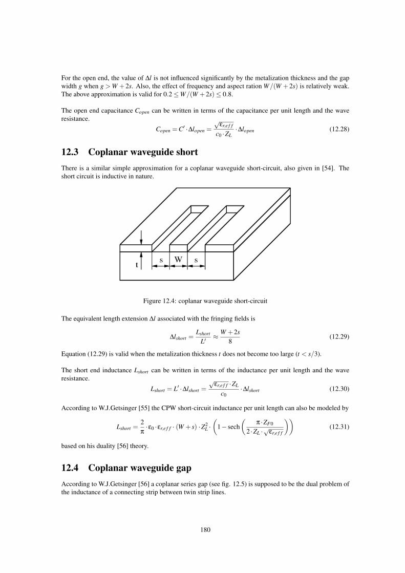
For the open end, the value of ∆l is not influenced significantly by the metalization thickness and the gapwidth g when g > W +2s. Also, the effect of frequency and aspect ration W/(W +2s) is relatively weak.The above approximation is valid for 0.2≤W/(W +2s)≤ 0.8.
The open end capacitance Copen can be written in terms of the capacitance per unit length and the waveresistance.
Copen = C′ ·∆lopen =√
εr,e f f
c0 ·ZL·∆lopen (12.28)
12.3 Coplanar waveguide shortThere is a similar simple approximation for a coplanar waveguide short-circuit, also given in [54]. Theshort circuit is inductive in nature.
Figure 12.4: coplanar waveguide short-circuit
The equivalent length extension ∆l associated with the fringing fields is
∆lshort =Lshort
L′≈ W +2s
8(12.29)
Equation (12.29) is valid when the metalization thickness t does not become too large (t < s/3).
The short end inductance Lshort can be written in terms of the inductance per unit length and the waveresistance.
Lshort = L′ ·∆lshort =√
εr,e f f ·ZL
c0·∆lshort (12.30)
According to W.J.Getsinger [55] the CPW short-circuit inductance per unit length can also be modeled by
Lshort =2π·ε0 ·εr,e f f · (W + s) ·Z2
L ·(
1− sech(
π ·ZF0
2 ·ZL ·√
εr,e f f
))(12.31)
based on his duality [56] theory.
12.4 Coplanar waveguide gapAccording to W.J.Getsinger [56] a coplanar series gap (see fig. 12.5) is supposed to be the dual problem ofthe inductance of a connecting strip between twin strip lines.
180
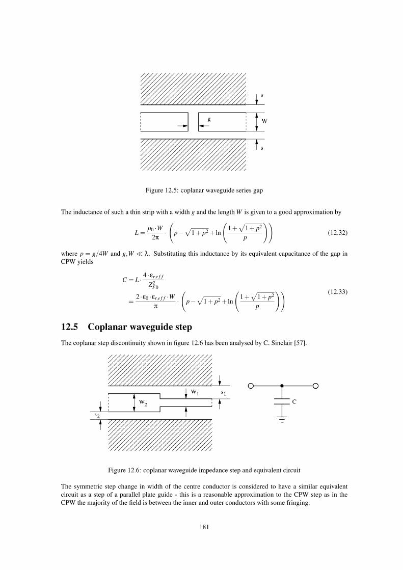
Figure 12.5: coplanar waveguide series gap
The inductance of such a thin strip with a width g and the length W is given to a good approximation by
L =µ0 ·W
2π·
(p−√
1+ p2 + ln
(1+√
1+ p2
p
))(12.32)
where p = g/4W and g,W λ. Substituting this inductance by its equivalent capacitance of the gap inCPW yields
C = L ·4 ·εr,e f f
Z2F0
=2 ·ε0 ·εr,e f f ·W
π·
(p−√
1+ p2 + ln
(1+√
1+ p2
p
)) (12.33)
12.5 Coplanar waveguide stepThe coplanar step discontinuity shown in figure 12.6 has been analysed by C. Sinclair [57].
Figure 12.6: coplanar waveguide impedance step and equivalent circuit
The symmetric step change in width of the centre conductor is considered to have a similar equivalentcircuit as a step of a parallel plate guide - this is a reasonable approximation to the CPW step as in theCPW the majority of the field is between the inner and outer conductors with some fringing.
181
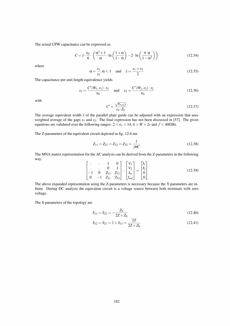
The actual CPW capacitance can be expressed as
C = x · ε0
π·(
α2 +1α· ln(
1+α
1−α
)−2 · ln
(4 ·α
1−α2
))(12.34)
whereα =
s1
s2,α < 1 and x =
x1 + x2
2(12.35)
The capacitance per unit length equivalence yields
x1 =C′ (W1,s1) ·s1
ε0and x2 =
C′ (W2,s2) ·s2
ε0(12.36)
with
C′ =√
εr,e f f
c0 ·ZL(12.37)
The average equivalent width x of the parallel plate guide can be adjusted with an expression that usesweighted average of the gaps s1 and s2. The final expression has not been discussed in [57]. The givenequations are validated over the following ranges: 2 < εr < 14, h > W +2s and f < 40GHz.
The Z-parameters of the equivalent circuit depicted in fig. 12.6 are
Z11 = Z21 = Z12 = Z22 =1
jωC(12.38)
The MNA matrix representation for the AC analysis can be derived from the Z-parameters in the followingway.
. . 1 0
. . 0 1−1 0 Z11 Z120 −1 Z21 Z22
·
V1V2IinIout
=
I1I200
(12.39)
The above expanded representation using the Z-parameters is necessary because the Y-parameters are in-finite. During DC analysis the equivalent circuit is a voltage source between both terminals with zerovoltage.
The S-parameters of the topology are
S11 = S22 =− Z0
2Z +Z0(12.40)
S12 = S21 = 1+S11 =2Z
2Z +Z0(12.41)
182
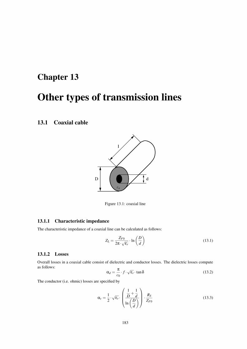
Chapter 13
Other types of transmission lines
13.1 Coaxial cable
Figure 13.1: coaxial line
13.1.1 Characteristic impedanceThe characteristic impedance of a coaxial line can be calculated as follows:
ZL =ZF0
2π ·√
εr· ln(
Dd
)(13.1)
13.1.2 LossesOverall losses in a coaxial cable consist of dielectric and conductor losses. The dielectric losses computeas follows:
αd =π
c0· f ·√
εr · tanδ (13.2)
The conductor (i.e. ohmic) losses are specified by
αc =12·√
εr ·
1D
+1d
ln(
Dd
) · RS
ZF0(13.3)
183
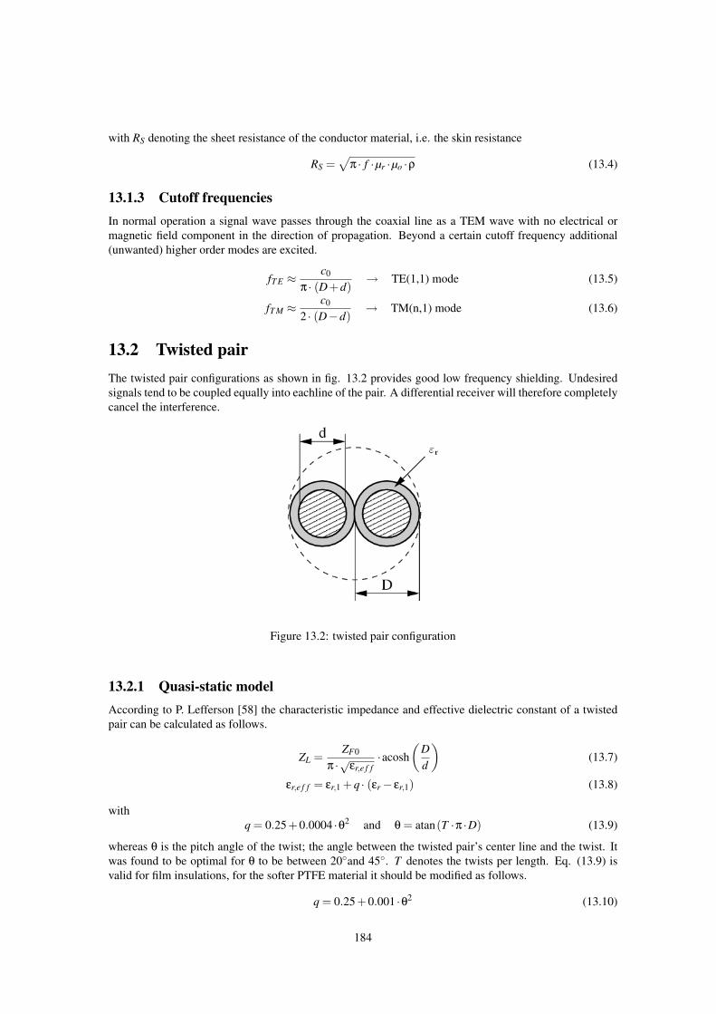
with RS denoting the sheet resistance of the conductor material, i.e. the skin resistance
RS =√
π · f ·µr ·µo ·ρ (13.4)
13.1.3 Cutoff frequenciesIn normal operation a signal wave passes through the coaxial line as a TEM wave with no electrical ormagnetic field component in the direction of propagation. Beyond a certain cutoff frequency additional(unwanted) higher order modes are excited.
fT E ≈c0
π · (D+d)→ TE(1,1) mode (13.5)
fT M ≈c0
2 · (D−d)→ TM(n,1) mode (13.6)
13.2 Twisted pairThe twisted pair configurations as shown in fig. 13.2 provides good low frequency shielding. Undesiredsignals tend to be coupled equally into eachline of the pair. A differential receiver will therefore completelycancel the interference.
Figure 13.2: twisted pair configuration
13.2.1 Quasi-static modelAccording to P. Lefferson [58] the characteristic impedance and effective dielectric constant of a twistedpair can be calculated as follows.
ZL =ZF0
π ·√εr,e f f·acosh
(Dd
)(13.7)
εr,e f f = εr,1 +q · (εr− εr,1) (13.8)
withq = 0.25+0.0004 ·θ2 and θ = atan(T ·π ·D) (13.9)
whereas θ is the pitch angle of the twist; the angle between the twisted pair’s center line and the twist. Itwas found to be optimal for θ to be between 20and 45. T denotes the twists per length. Eq. (13.9) isvalid for film insulations, for the softer PTFE material it should be modified as follows.
q = 0.25+0.001 ·θ2 (13.10)
184
Assuming air as dielectric around the wires yields 1’s replacing εr,1 in eq. (13.8). The wire’s total lengthbefore twisting in terms of the number of turns N is
l = N ·π ·D ·√
1+1
tan2 θ(13.11)
13.2.2 Transmission lossesThe propagation constant γ of a general transmission line is given by
γ =√
(R′+ jωL′) · (G′+ jωC′) (13.12)
Using some transformations of the formula gives an expression with and without the angular frequency.
γ =√
(R′+ jωL′) · (G′+ jωC′)
=√
L′C′ ·
√R′G′
L′C′+ jω
(R′
L′+
G′
C′
)−ω2
=√
L′C′ ·
√(12·(
R′
L′+
G′
C′
)+ jω
)2
− 14·(
R′
L′+
G′
C′
)2
+R′G′
L′C′
(13.13)
For high frequencies eq.(13.13) can be approximated to
γ≈√
L′C′ ·(
12·(
R′
L′+
G′
C′
)+ jω
)(13.14)
Thus the real part of the propagation constant γ yields
α = Reγ=√
L′C′ · 12·(
R′
L′+
G′
C′
)(13.15)
With
ZL =
√L′
C′(13.16)
the expression in eq.(13.15) can be written as
α = αc +αd =12·(
R′
ZL+G′ZL
)(13.17)
whereas αc denotes the conductor losses and αd the dielectric losses.
Conductor losses
The sheet resistance R’ of a transmission line conductor is given by
R′ =ρ
Ae f f(13.18)
whereas ρ is the specific resistance of the conductor material and Ae f f the effective area of the conductorperpendicular to the propagation direction. At higher frequencies the area of the conductor is reduced bythe skin effect. The skin depth is given by
δs =√
ρ
π · f ·µ(13.19)
Thus the effective area of a single round wire yields
Ae f f = π ·(r2− (r−δs)2) (13.20)
whereas r denotes the radius of the wire. This means the overall conductor attenuation constant αc for asingle wire gives
αc =R′
2 ·ZL=
ρ
2 ·ZL ·π · (r2− (r−δs)2)(13.21)
185
Dielectric losses
The dielectric losses are determined by the dielectric loss tangent.
tanδd =G′
ωC′→ G′ = ωC′ · tanδd (13.22)
With
C′ =1ω· Im
γ
ZL
(13.23)
the equation (13.22) can be rewritten to
G′ =β
ZL· tanδd =
ω
vph ·ZL· tanδd
=2π · f ·√εr,e f f
c0 ·ZL· tanδd =
2π ·√εr,e f f
λ0 ·ZL· tanδd
(13.24)
whereas vph denotes the phase velocity, c0 the speed of light, εr,e f f the effective dielectric constant and λ0the freespace wavelength. With these expressions at hand it is possible to find a formula for the dielectriclosses of the transmission line.
αd =12·G′ZL =
π ·√εr,e f f
λ0· tanδd (13.25)
Overall losses of the twisted pair configuration
Transmission losses consist of conductor losses, dielectric losses as well as radiation losses. The aboveexpressions for the conductor and dielectric losses are considered to be first order approximations. Theconductor losses have been derived for a single round wire. The overall conductor losses due to the twinwires must be doubled. The dielectric losses can be used as is. Radiation losses are neglected.
186
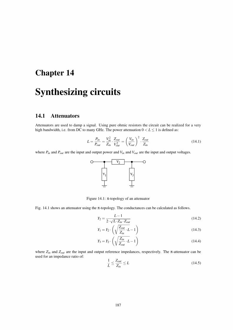
Chapter 14
Synthesizing circuits
14.1 AttenuatorsAttenuators are used to damp a signal. Using pure ohmic resistors the circuit can be realized for a veryhigh bandwidth, i.e. from DC to many GHz. The power attenuation 0 < L≤ 1 is defined as:
L =Pin
Pout=
V 2in
Zin· Zout
V 2out
=(
Vin
Vout
)2
· Zout
Zin(14.1)
where Pin and Pout are the input and output power and Vin and Vout are the input and output voltages.
Figure 14.1: π-topology of an attenuator
Fig. 14.1 shows an attenuator using the π-topology. The conductances can be calculated as follows.
Y2 =L−1
2 ·√
L ·Zin ·Zout(14.2)
Y1 = Y2 ·(√
Zout
Zin·L−1
)(14.3)
Y3 = Y2 ·(√
Zin
Zout·L−1
)(14.4)
where Zin and Zout are the input and output reference impedances, respectively. The π-attenuator can beused for an impedance ratio of:
1L≤ Zout
Zin≤ L (14.5)
187
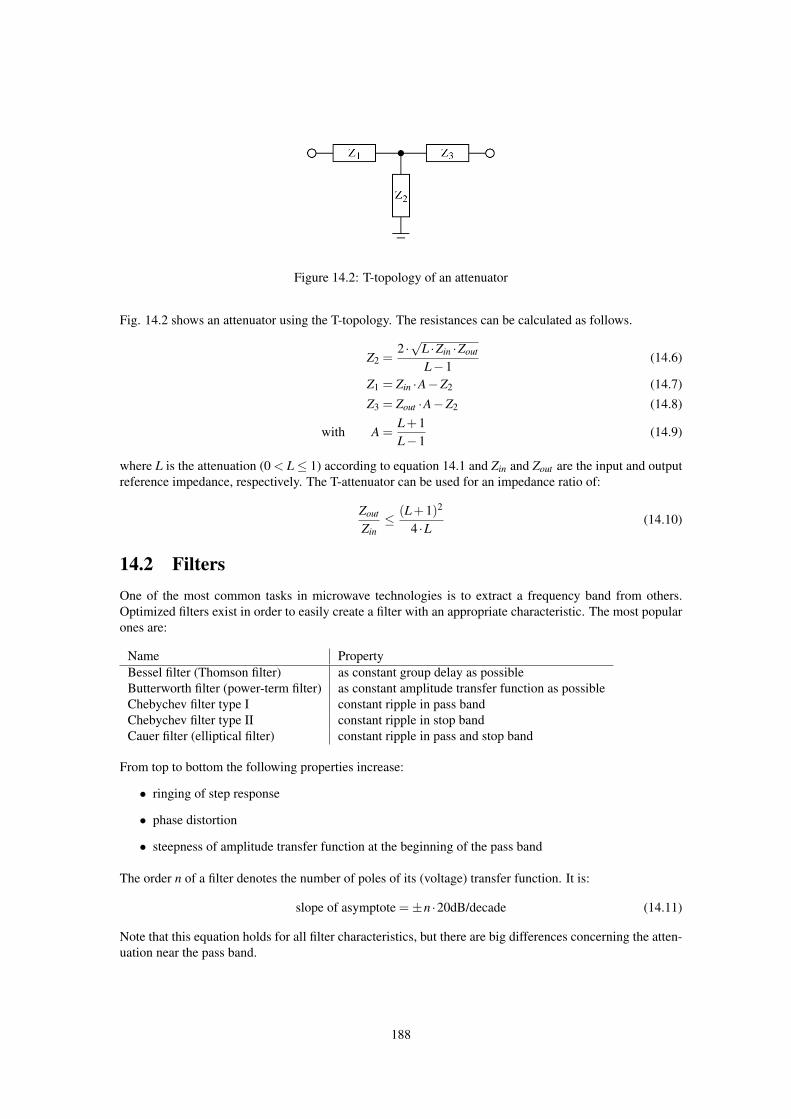
Figure 14.2: T-topology of an attenuator
Fig. 14.2 shows an attenuator using the T-topology. The resistances can be calculated as follows.
Z2 =2 ·√
L ·Zin ·Zout
L−1(14.6)
Z1 = Zin ·A−Z2 (14.7)Z3 = Zout ·A−Z2 (14.8)
with A =L+1L−1
(14.9)
where L is the attenuation (0 < L≤ 1) according to equation 14.1 and Zin and Zout are the input and outputreference impedance, respectively. The T-attenuator can be used for an impedance ratio of:
Zout
Zin≤ (L+1)2
4 ·L(14.10)
14.2 FiltersOne of the most common tasks in microwave technologies is to extract a frequency band from others.Optimized filters exist in order to easily create a filter with an appropriate characteristic. The most popularones are:
Name PropertyBessel filter (Thomson filter) as constant group delay as possibleButterworth filter (power-term filter) as constant amplitude transfer function as possibleChebychev filter type I constant ripple in pass bandChebychev filter type II constant ripple in stop bandCauer filter (elliptical filter) constant ripple in pass and stop band
From top to bottom the following properties increase:
• ringing of step response
• phase distortion
• steepness of amplitude transfer function at the beginning of the pass band
The order n of a filter denotes the number of poles of its (voltage) transfer function. It is:
slope of asymptote =±n ·20dB/decade (14.11)
Note that this equation holds for all filter characteristics, but there are big differences concerning the atten-uation near the pass band.
188
14.2.1 LC ladder filtersThe best possibility to realize a filters in VHF and UHF bands are LC ladder filters. The usual way tosynthesize them is to first calculate a low-pass (LP) filter and afterwards transform it into a high-pass (HP),band-pass (BP) or band-stop (BS) filter. To do so, each component must be transformed into another.
In a low-pass filter, there are parallel capacitors CLP and series inductors LLP in alternating order. The otherfilter classes can be derived from it:
In a high-pass filter:
CLP → LHP =1
ω2B ·CLP
(14.12)
LLP → CHP =1
ω2B ·LLP
(14.13)
In a band-pass filter:
CLP → parallel resonance circuit with (14.14)
CBP =CLP
∆Ω(14.15)
LBP =∆Ω
ω1 ·ω2 ·CLP(14.16)
LLP → series resonance circuit with (14.17)
CBP =∆Ω
ω1 ·ω2 ·LLP(14.18)
LBP =LLP
∆Ω(14.19)
In a band-stop filter:
CLP → series resonance circuit with (14.20)
CBP =CLP
2 ·∣∣∣∣ω2
ω1− ω1
ω2
∣∣∣∣ (14.21)
LBP =1
ω2 ·∆Ω ·CLP(14.22)
LLP → parallel resonance circuit with (14.23)
CBP =1
ω2 ·∆Ω ·LLP(14.24)
LBP =LLP
2 ·∣∣∣∣ω2
ω1− ω1
ω2
∣∣∣∣ (14.25)
Where
ω1 → lower corner frequency of frequency band (14.26)ω2 → upper corner frequency of frequency band (14.27)ω → center frequency of frequency band ω = 0.5 ·(ω1 +ω2) (14.28)
∆Ω → ∆Ω =|ω2−ω1|
ω(14.29)
189
Butterworth
The k-th element of an n order Butterworth low-pass ladder filter is:
capacitance: Ck =Xk
Z0(14.30)
inductance: Lk =Xk ·Z0 (14.31)
with Xk =2
ωB· sin
(2 ·k +1) ·π2 ·n
(14.32)
The order of the Butterworth filter is dependent on the specifications provided by the user. These specifi-cations include the edge frequencies and gains.
n =log(
10−0.1·αstop −110−0.1·αpass −1
)2 · log
(ωstop
ωpass
) (14.33)
Chebyshev I
The equations for a Chebyshev type I filter are defined recursivly. With RdB being the passband ripple indecibel, the k-th element of an n order low-pass ladder filter is:
capacitance: Ck =Xk
Z0(14.34)
inductance: Lk = Xk ·Z0 (14.35)
with Xk =2
ωB·gk (14.36)
r = sinh
(1n·arsinh
1√10RdB/10−1
)(14.37)
ak = sin(2 ·k +1) ·π
2 ·n(14.38)
gk =
ak
rfor k = 0
ak−1 ·ak
gk−1 ·(
r2 + sin2 k ·πn
) for k ≥ 1 (14.39)
Xk =2
ωB·gk (14.40)
The order of the Chebychev filter is dependent on the specifications provided by the user. The general formof the calculation for the order is the same as for the Butterworth, except that the inverse hyperbolic cosinefunction is used in place of the common logarithm function.
n =sech
(10−0.1·αstop −110−0.1·αpass −1
)2 ·sech
(ωstop
ωpass
) (14.41)
Chebyshev II
Because of the nature of the derivation of the inverse Chebychev approxiation function from the standardChebychev approximation the calculation of the order (14.41) is the same.
190
Chapter 15
Mathematical background
15.1 N-port matrix conversionsWhen dealing with n-port parameters it may be necessary or convenient to convert them into other ma-trix representations used in electrical engineering. The following matrices and notations are used in thetransformation equations.
[X ]−1 = inverted matrix of [X ]
[X ]∗ = complex conjugated matrix of [X ]
[E] =
1 0 . . . 00 1 . . . 0...
.... . .
...0 0 . . . 1
identity matrix
[S] = S-parameter matrix
[Z] = impedance matrix
[Y ] = admittance matrix
[Zre f
]=
Z0,1 0 . . . 0
0 Z0,2 . . . 0...
.... . .
...0 0 . . . Z0,N
Z0,n = reference impedance of port n
[Gre f ] =
G1 0 . . . 00 G2 . . . 0...
.... . .
...0 0 . . . GN
Gn =
1√Re∣∣Z0,n
∣∣
191
15.1.1 Renormalization of S-parameters to different port impedancesDuring S-parameter usage it sometimes appears to have not all components in a circuit normalized to thesame impedance. But calculations can only be performed with all ports being normalized to the sameimpedance. In the field of high frequency techniques this is usually 50Ω. In order to transform to differentport impedances, the following computation must be applied to the resulting S-parameter matrix.[
S′]= [A]−1 · ([S]− [R]) · ([E]− [R] · [S])−1 · [A] (15.1)
With
Zn = reference impedance of port n after the normalizing process
Zn,be f ore = reference impedance of port n before the normalizing process
[S] = original S-parameter matrix
[S′] = recalculated scattering matrix
[R] =
r (Z1) 0 . . . 0
0 r (Z2) . . . 0...
.... . .
...0 0 . . . r (ZN)
reflection coefficient matrix
r (Zn) =Zn−Zn,be f ore
Zn +Zn,be f ore
[A] =
A1 0 . . . 00 A2 . . . 0...
.... . .
...0 0 . . . AN
An =
√Zn
Zn,be f ore· 1
Zn +Zn,be f ore
15.1.2 Transformations of n-Port matricesS-parameter, admittance and impedance matrices are not limited to One- or Two-Port definitions. They aredefined for an arbitrary number of ports. The following section contains transformation formulas forth andback each matrix representation.
Converting a scattering parameter matrix to an impedance matrix is done by the following formula.
[Z] =[Gre f
]−1 · ([E]− [S])−1 ·([S] ·
[Zre f
]+[Zre f
])·[Gre f
](15.2)
=[Gre f
]−1 · ([E]− [S])−1 · ([S]+ [E]) ·[Zre f
]·[Gre f
](15.3)
Converting a scattering parameter matrix to an admittance matrix can be achieved by computing the fol-lowing formula.
[Y ] =[Gre f
]−1 ·([S] ·
[Zre f
]+[Zre f
])−1 · ([E]− [S]) ·[Gre f
](15.4)
=[Gre f
]−1 ·[Zre f
]−1 · ([S]+ [E])−1 · ([E]− [S]) ·[Gre f
](15.5)
192
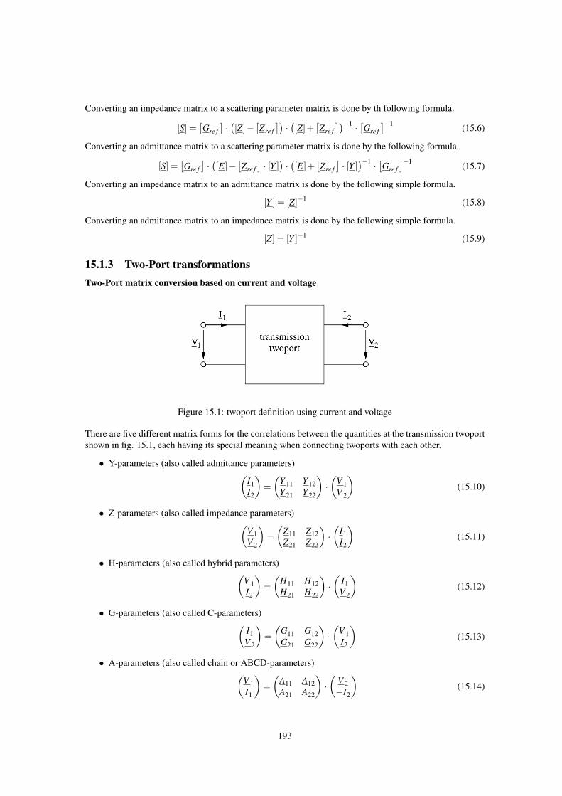
Converting an impedance matrix to a scattering parameter matrix is done by th following formula.
[S] =[Gre f
]·([Z]−
[Zre f
])·([Z]+
[Zre f
])−1 ·[Gre f
]−1 (15.6)
Converting an admittance matrix to a scattering parameter matrix is done by the following formula.
[S] =[Gre f
]·([E]−
[Zre f
]· [Y ]
)·([E]+
[Zre f
]· [Y ]
)−1 ·[Gre f
]−1 (15.7)
Converting an impedance matrix to an admittance matrix is done by the following simple formula.
[Y ] = [Z]−1 (15.8)
Converting an admittance matrix to an impedance matrix is done by the following simple formula.
[Z] = [Y ]−1 (15.9)
15.1.3 Two-Port transformationsTwo-Port matrix conversion based on current and voltage
Figure 15.1: twoport definition using current and voltage
There are five different matrix forms for the correlations between the quantities at the transmission twoportshown in fig. 15.1, each having its special meaning when connecting twoports with each other.
• Y-parameters (also called admittance parameters)(I1I2
)=(
Y 11 Y 12Y 21 Y 22
)·(
V 1V 2
)(15.10)
• Z-parameters (also called impedance parameters)(V 1V 2
)=(
Z11 Z12Z21 Z22
)·(
I1I2
)(15.11)
• H-parameters (also called hybrid parameters)(V 1I2
)=(
H11 H12H21 H22
)·(
I1V 2
)(15.12)
• G-parameters (also called C-parameters)(I1V 2
)=(
G11 G12G21 G22
)·(
V 1I2
)(15.13)
• A-parameters (also called chain or ABCD-parameters)(V 1I1
)=(
A11 A12A21 A22
)·(
V 2−I2
)(15.14)
193
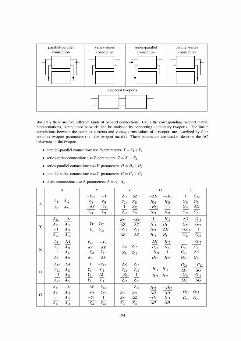
parallel-parallelconnection
series-seriesconnection
series-parallelconnection
parallel-seriesconnection
cascaded twoports
Basically there are five different kinds of twoport connections. Using the corresponding twoport matrixrepresentations, complicated networks can be analysed by connecting elementary twoports. The linearcorrelations between the complex currents and voltages rms values of a twoport are described by fourcomplex twoport parameters (i.e. the twoport matrix). These parameters are used to describe the ACbehaviour of the twoport.
• parallel-parallel connection: use Y-parameters: Y = Y1 +Y2
• series-series connection: use Z-parameters: Z = Z1 +Z2
• series-parallel connection: use H-parameters: H = H1 +H2
• parallel-series connection: use G-parameters: G = G1 +G2
• chain connection: use A-parameters: A = A1 ·A2
A Y Z H G
AA11 A12
A21 A22
−Y22
Y21
−1Y21
−∆YY21
−Y11
Y21
Z11
Z21
∆ZZ21
1Z21
Z22
Z21
−∆HH21
−H11
H21−H22
H21
−1H21
1G21
G22
G21G11
G21
∆GG21
Y
A22
A12
−∆AA12
−1A12
A11
A12
Y11 Y12
Y21 Y22
Z22
∆Z−Z12
∆Z−Z21
∆ZZ11
∆Z
1H11
−H12
H11H21
H11
∆HH11
∆GG22
G12
G22−G21
G22
1G22
Z
A11
A21
∆AA21
1A21
A22
A21
Y22
∆Y−Y12
∆Y−Y21
∆YY11
∆Y
Z11 Z12
Z21 Z22
∆HH22
H12
H22−H21
H22
1H22
1G11
−G12
G11G21
G11
∆GG11
H
A12
A22
∆AA22
−1A22
A21
A22
1Y11
−Y12
Y11Y21
Y11
∆YY11
∆ZZ22
Z12
Z22−Z21
Z22
1Z22
H11 H12
H21 H22
G22
∆G−G12
∆G−G21
∆GG11
∆G
G
A21
A11
−∆AA11
1A11
A12
A11
∆YY22
Y12
Y22−Y21
Y22
1Y22
1Z11
−Z12
Z11Z21
Z11
∆ZZ11
H22
∆H−H12
∆H−H21
∆HH11
∆H
G11 G12
G21 G22
194
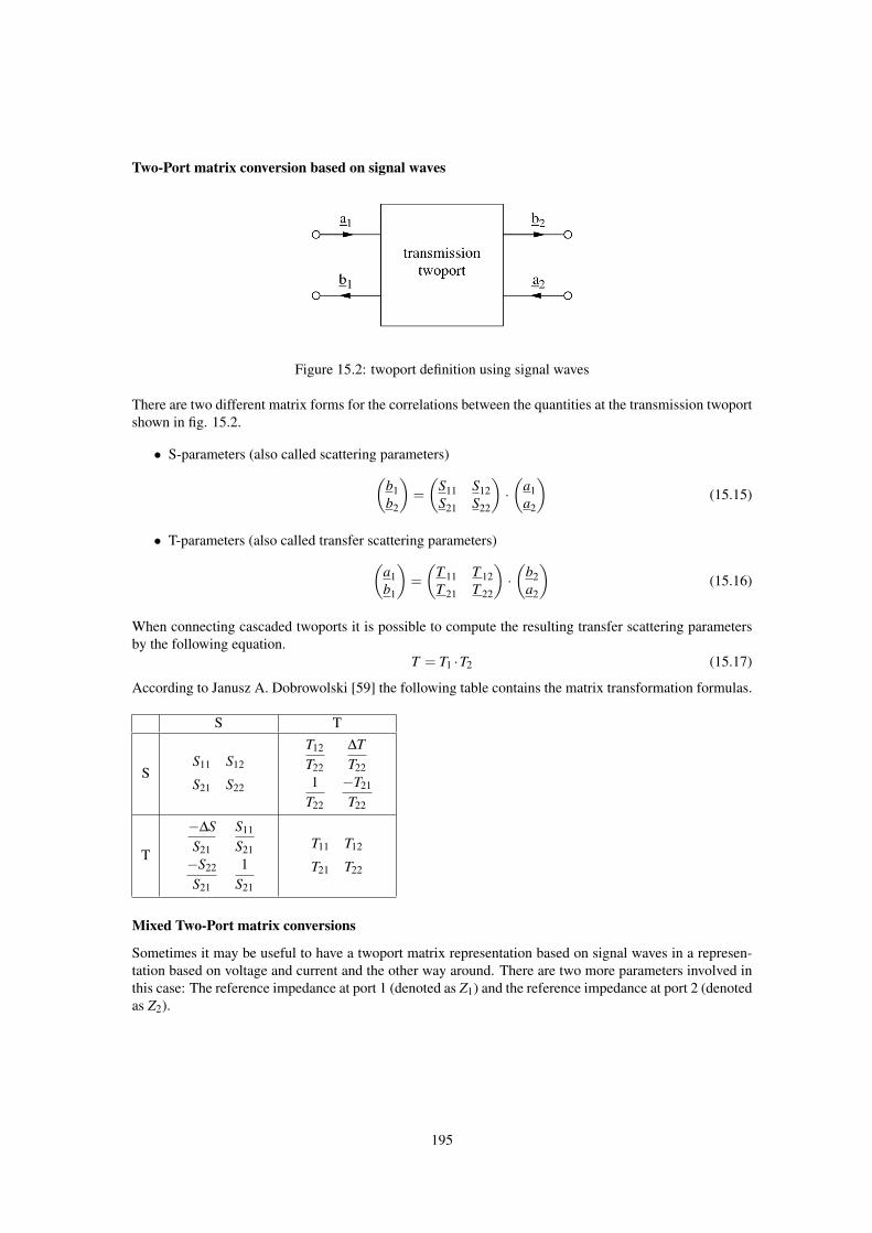
Two-Port matrix conversion based on signal waves
Figure 15.2: twoport definition using signal waves
There are two different matrix forms for the correlations between the quantities at the transmission twoportshown in fig. 15.2.
• S-parameters (also called scattering parameters)(b1b2
)=(
S11 S12S21 S22
)·(
a1a2
)(15.15)
• T-parameters (also called transfer scattering parameters)(a1b1
)=(
T 11 T 12T 21 T 22
)·(
b2a2
)(15.16)
When connecting cascaded twoports it is possible to compute the resulting transfer scattering parametersby the following equation.
T = T1 ·T2 (15.17)
According to Janusz A. Dobrowolski [59] the following table contains the matrix transformation formulas.
S T
SS11 S12
S21 S22
T12
T22
∆TT22
1T22
−T21
T22
T
−∆SS21
S11
S21−S22
S21
1S21
T11 T12
T21 T22
Mixed Two-Port matrix conversions
Sometimes it may be useful to have a twoport matrix representation based on signal waves in a represen-tation based on voltage and current and the other way around. There are two more parameters involved inthis case: The reference impedance at port 1 (denoted as Z1) and the reference impedance at port 2 (denotedas Z2).
195
Converting from scattering parameters to chain parameters results in
A11 =Z∗1 +Z1 ·S11−Z∗1 ·S22−Z1 ·∆S
2 ·S21 ·√
Re(Z1) ·Re(Z2)(15.18)
A12 =Z∗1 ·Z∗2 +Z1 ·Z∗2 ·S11 +Z∗1 ·Z2 ·S22 +Z1 ·Z2 ·∆S
2 ·S21 ·√
Re(Z1) ·Re(Z2)(15.19)
A21 =1−S11−S22 +∆S
2 ·S21 ·√
Re(Z1) ·Re(Z2)(15.20)
A22 =Z∗2 −Z∗2 ·S11 +Z2 ·S22−Z2 ·∆S
2 ·S21 ·√
Re(Z1) ·Re(Z2)(15.21)
Converting from chain parameters to scattering parameters results in
S11 =A11 ·Z2 +A12−A21 ·Z∗1 ·Z2−A22 ·Z∗1A11 ·Z2 +A12 +A21 ·Z1 ·Z2 +A22 ·Z1
(15.22)
S12 =∆A ·2 ·
√Re(Z1) ·Re(Z2)
A11 ·Z2 +A12 +A21 ·Z1 ·Z2 +A22 ·Z1(15.23)
S21 =2 ·√
Re(Z1) ·Re(Z2)A11 ·Z2 +A12 +A21 ·Z1 ·Z2 +A22 ·Z1
(15.24)
S22 =−A11 ·Z∗2 +A12−A21 ·Z1 ·Z∗2 +A22 ·Z1
A11 ·Z2 +A12 +A21 ·Z1 ·Z2 +A22 ·Z1(15.25)
Converting from scattering parameters to hybrid parameters results in
H11 = Z1 ·(1+S11) · (1+S22)−S12 ·S21
(1−S11) · (1+S22)+S12 ·S21(15.26)
H12 =√
Z1
Z2· 2 ·S12
(1−S11) · (1+S22)+S12 ·S21(15.27)
H21 =√
Z1
Z2· −2 ·S21
(1−S11) · (1+S22)+S12 ·S21(15.28)
H22 =1Z2· (1−S11) · (1−S22)−S12 ·S21
(1−S11) · (1+S22)+S12 ·S21(15.29)
Converting from hybrid parameters to scattering parameters results in
S11 =(H11−Z1) · (1+Z2 ·H22)−Z2 ·H12 ·H21
(H11 +Z1) · (1+Z2 ·H22)−Z2 ·H12 ·H21(15.30)
S12 =2 ·H12 ·
√Z1 ·Z2
(H11 +Z1) · (1+Z2 ·H22)−Z2 ·H12 ·H21(15.31)
S21 =−2 ·H21 ·
√Z1 ·Z2
(H11 +Z1) · (1+Z2 ·H22)−Z2 ·H12 ·H21(15.32)
S22 =(H11 +Z1) · (1−Z2 ·H22)+Z2 ·H12 ·H21
(H11 +Z1) · (1+Z2 ·H22)−Z2 ·H12 ·H21(15.33)
196
Converting from scattering parameters to the second type of hybrid parameters results in
G11 =1Z1· (1−S11) · (1−S22)−S12 ·S21
(1+S11) · (1−S22)+S12 ·S21(15.34)
G12 =√
Z2
Z1· −2 ·S12
(1+S11) · (1−S22)+S12 ·S21(15.35)
G21 =√
Z2
Z1· 2 ·S21
(1+S11) · (1−S22)+S12 ·S21(15.36)
G22 = Z2 ·(1+S11) · (1+S22)−S12 ·S21
(1+S11) · (1−S22)+S12 ·S21(15.37)
Converting from the second type of hybrid parameters to scattering parameters results in
S11 =(1−G11 ·Z1) · (G22 +Z2)+Z1 ·G12 ·G21
(1+G11 ·Z1) · (G22 +Z2)−Z1 ·G12 ·G21(15.38)
S12 =−2 ·G12 ·
√Z1 ·Z2
(1+G11 ·Z1) · (G22 +Z2)−Z1 ·G12 ·G21(15.39)
S21 =2 ·G21 ·
√Z1 ·Z2
(1+G11 ·Z1) · (G22 +Z2)−Z1 ·G12 ·G21(15.40)
S22 =(1+G11 ·Z1) · (G22−Z2)−Z1 ·G12 ·G21
(1+G11 ·Z1) · (G22 +Z2)−Z1 ·G12 ·G21(15.41)
Converting from scattering parameters to Y-parameters results in
Y11 =1Z1· (1−S11) · (1+S22)+S12 ·S21
(1+S11) · (1+S22)−S12 ·S21(15.42)
Y12 =√
1Z1 ·Z2
· −2 ·S12
(1+S11) · (1+S22)−S12 ·S21(15.43)
Y21 =√
1Z1 ·Z2
· −2 ·S21
(1+S11) · (1+S22)−S12 ·S21(15.44)
Y22 =1Z2· (1+S11) · (1−S22)+S12 ·S21
(1+S11) · (1+S22)−S12 ·S21(15.45)
Converting from Y-parameters to scattering parameters results in
S11 =(1−Y11 ·Z1) · (1+Y22 ·Z2)+Y12 ·Z1 ·Y21 ·Z2
(1+Y11 ·Z1) · (1+Y22 ·Z2)−Y12 ·Z1 ·Y21 ·Z2(15.46)
S12 =−2 ·Y12 ·
√Z1 ·Z2
(1+Y11 ·Z1) · (1+Y22 ·Z2)−Y12 ·Z1 ·Y21 ·Z2(15.47)
S21 =−2 ·Y21 ·
√Z1 ·Z2
(1+Y11 ·Z1) · (1+Y22 ·Z2)−Y12 ·Z1 ·Y21 ·Z2(15.48)
S22 =(1+Y11 ·Z1) · (1−Y22 ·Z2)+Y12 ·Z1 ·Y21 ·Z2
(1+Y11 ·Z1) · (1+Y22 ·Z2)−Y12 ·Z1 ·Y21 ·Z2(15.49)
197
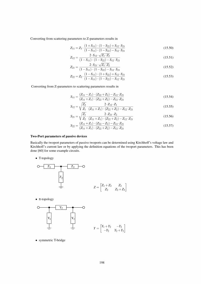
Converting from scattering parameters to Z-parameters results in
Z11 = Z1 ·(1+S11) · (1−S22)+S12 ·S21
(1−S11) · (1−S22)−S12 ·S21(15.50)
Z12 =2 ·S12 ·
√Z1 ·Z2
(1−S11) · (1−S22)−S12 ·S21(15.51)
Z21 =2 ·S21 ·
√Z1 ·Z2
(1−S11) · (1−S22)−S12 ·S21(15.52)
Z22 = Z2 ·(1−S11) · (1+S22)+S12 ·S21
(1−S11) · (1−S22)−S12 ·S21(15.53)
Converting from Z-parameters to scattering parameters results in
S11 =(Z11−Z1) · (Z22 +Z2)−Z12 ·Z21
(Z11 +Z1) · (Z22 +Z2)−Z12 ·Z21(15.54)
S12 =√
Z2
Z1· 2 ·Z12 ·Z1
(Z11 +Z1) · (Z22 +Z2)−Z12 ·Z21(15.55)
S21 =√
Z1
Z2· 2 ·Z21 ·Z2
(Z11 +Z1) · (Z22 +Z2)−Z12 ·Z21(15.56)
S22 =(Z11 +Z1) · (Z22−Z2)−Z12 ·Z21
(Z11 +Z1) · (Z22 +Z2)−Z12 ·Z21(15.57)
Two-Port parameters of passive devices
Basically the twoport parameters of passive twoports can be determined using Kirchhoff’s voltage law andKirchhoff’s current law or by applying the definition equations of the twoport parameters. This has beendone [60] for some example circuits.
• T-topology
Z =[
Z1 +Z2 Z2Z2 Z2 +Z3
]
• π-topology
Y =[Y1 +Y2 −Y2−Y2 Y2 +Y3
]
• symmetric T-bridge
198
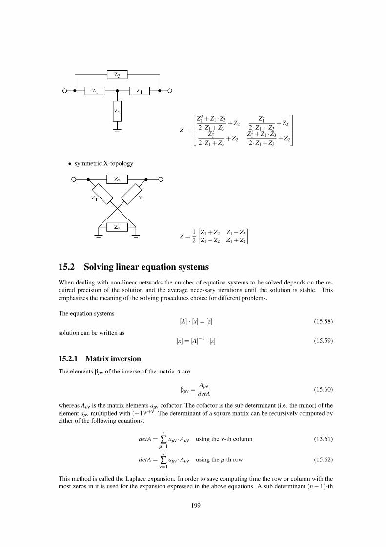
Z =
Z2
1 +Z1 ·Z3
2 ·Z1 +Z3+Z2
Z21
2 ·Z1 +Z3+Z2
Z21
2 ·Z1 +Z3+Z2
Z21 +Z1 ·Z3
2 ·Z1 +Z3+Z2
• symmetric X-topology
Z =12
[Z1 +Z2 Z1−Z2Z1−Z2 Z1 +Z2
]
15.2 Solving linear equation systemsWhen dealing with non-linear networks the number of equation systems to be solved depends on the re-quired precision of the solution and the average necessary iterations until the solution is stable. Thisemphasizes the meaning of the solving procedures choice for different problems.
The equation systems[A] · [x] = [z] (15.58)
solution can be written as[x] = [A]−1 · [z] (15.59)
15.2.1 Matrix inversionThe elements βµν of the inverse of the matrix A are
βµν =Aµν
detA(15.60)
whereas Aµν is the matrix elements aµν cofactor. The cofactor is the sub determinant (i.e. the minor) of theelement aµν multiplied with (−1)µ+ν. The determinant of a square matrix can be recursively computed byeither of the following equations.
detA =n
∑µ=1
aµν ·Aµν using the ν-th column (15.61)
detA =n
∑ν=1
aµν ·Aµν using the µ-th row (15.62)
This method is called the Laplace expansion. In order to save computing time the row or column with themost zeros in it is used for the expansion expressed in the above equations. A sub determinant (n−1)-th
199
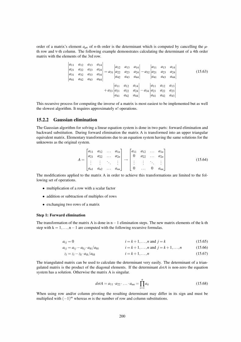
order of a matrix’s element aµν of n-th order is the determinant which is computed by cancelling the µ-th row and ν-th column. The following example demonstrates calculating the determinant of a 4th ordermatrix with the elements of the 3rd row.∣∣∣∣∣∣∣∣
a11 a12 a13 a14a21 a22 a23 a24a31 a32 a33 a34a41 a42 a43 a44
∣∣∣∣∣∣∣∣= a31
∣∣∣∣∣∣a12 a13 a14a22 a23 a24a42 a43 a44
∣∣∣∣∣∣−a32
∣∣∣∣∣∣a11 a13 a14a21 a23 a24a41 a43 a44
∣∣∣∣∣∣ (15.63)
+a33
∣∣∣∣∣∣a11 a12 a14a21 a22 a24a41 a42 a44
∣∣∣∣∣∣−a34
∣∣∣∣∣∣a11 a12 a13a21 a22 a23a41 a42 a43
∣∣∣∣∣∣This recursive process for computing the inverse of a matrix is most easiest to be implemented but as wellthe slowest algorithm. It requires approximately n! operations.
15.2.2 Gaussian eliminationThe Gaussian algorithm for solving a linear equation system is done in two parts: forward elimination andbackward substitution. During forward elimination the matrix A is transformed into an upper triangularequivalent matrix. Elementary transformations due to an equation system having the same solutions for theunknowns as the original system.
A =
a11 a12 . . . a1na21 a22 . . . a2n
......
. . ....
an1 an2 . . . ann
→
a11 a12 . . . a1n0 a22 . . . a2n...
.... . .
...0 . . . 0 ann
(15.64)
The modifications applied to the matrix A in order to achieve this transformations are limited to the fol-lowing set of operations.
• multiplication of a row with a scalar factor
• addition or subtraction of multiples of rows
• exchanging two rows of a matrix
Step 1: Forward elimination
The transformation of the matrix A is done in n−1 elimination steps. The new matrix elements of the k-thstep with k = 1, . . . ,n−1 are computed with the following recursive formulas.
ai j = 0 i = k +1, . . . ,n and j = k (15.65)ai j = ai j−ak j ·aik/akk i = k +1, . . . ,n and j = k +1, . . . ,n (15.66)zi = zi− zk ·aik/akk i = k +1, . . . ,n (15.67)
The triangulated matrix can be used to calculate the determinant very easily. The determinant of a trian-gulated matrix is the product of the diagonal elements. If the determinant detA is non-zero the equationsystem has a solution. Otherwise the matrix A is singular.
detA = a11 ·a22 · . . . ·ann =n
∏i=1
aii (15.68)
When using row and/or column pivoting the resulting determinant may differ in its sign and must bemultiplied with (−1)m whereas m is the number of row and column substitutions.
200
Finding an appropriate pivot element
The Gaussian elimination fails if the pivot element akk turns to be zero (division by zero). That is whyrow and/or column pivoting must be used before each elimination step. If a diagonal element akk = 0, thenexchange the pivot row k with the row m > k having the coefficient with the largest absolute value. Thenew pivot row is m and the new pivot element is going to be amk. If no such pivot row can be found thematrix is singular.
Total pivoting looks for the element with the largest absolute value within the matrix and exchanges rowsand columns. When exchanging columns in equation systems the unknowns get reordered as well. Forthe numerical solution of equation systems with Gaussian elimination column pivoting is clever, and totalpivoting recommended.
In order to improve numerical stability pivoting should also be applied if akk 6= 0 because division by smalldiagonal elements propagates numerical (rounding) errors. This appears especially with poorly conditioned(the two dimensional case: two lines with nearly the same slope) equation systems.
Step 2: Backward substitution
The solutions in the vector x are obtained by backward substituting into the triangulated matrix. Theelements of the solution vector x are computed by the following recursive equations.
xn =zn
ann(15.69)
xi =zi
aii−
n
∑k=i+1
xk ·aik
aiii = n−1, . . . ,1 (15.70)
The forward elimination in the Gaussian algorithm requires approximately n3/3, the backward substitutionn2/2 operations.
15.2.3 Gauss-Jordan methodThe Gauss-Jordan method is a modification of the Gaussian elimination. In each k-th elimination step theelements of the k-th column get zero except the diagonal element which gets 1. When the right hand sidevector z is included in each step it contains the solution vector x afterwards.
The following recursive formulas must be applied to get the new matrix elements for the k-th eliminationstep. The k-th row must be computed first.
ak j = ak j/akk j = 1 . . .n (15.71)zk = zk/akk (15.72)
Then the other rows can be calculated with the following formulas.
ai j = ai j−aik ·ak j j = 1, . . . ,n and i = 1, . . . ,n with i 6= k (15.73)zi = zi−aik ·zk i = 1, . . . ,n with i 6= k (15.74)
Column pivoting may be necessary in order to avoid division by zero. The solution vector x is not harmedby row substitutions. When the Gauss-Jordan algorithm has been finished the original matrix has beentransformed into the identity matrix. If each operation during this process is applied to an identity matrixthe resulting matrix is the inverse matrix of the original matrix. This means that the Gauss-Jordan methodcan be used to compute the inverse of a matrix.
Though this elimination method is easy to implement the number of required operations is larger thanwithin the Gaussian elimination. The Gauss-Jordan method requires approximately N3/2 + N2/2 opera-tions.
201
15.2.4 LU decompositionLU decomposition (decomposition into a lower and upper triangular matrix) is recommended when dealingwith equation systems where the matrix A does not alter but the right hand side (the vector z) does. Boththe Gaussian elimination and the Gauss-Jordan method involve both the right hand side and the matrixin their algorithm. Consecutive solutions of an equation system with an altering right hand side can becomputed faster with LU decomposition.
The LU decomposition splits a matrix A into a product of a lower triangular matrix L with an uppertriangular matrix U.
A = LU with L =
l11 0 . . . 0
l21 l22. . .
......
. . . 0ln1 . . . . . . lnn
and U =
u11 u12 . . . u1n
0 u22...
.... . . . . .
...0 . . . 0 unn
(15.75)
The algorithm for solving the linear equation system Ax = z involves three steps:
• LU decomposition of the coefficient matrix A→ Ax = LUx = z
• introduction of an (unknown) arbitrary vector y and solving the equation system Ly = z by forwardsubstitution→ y = Ux = L−1z
• solving the equation system Ux = y by backward substitution→ x = U−1y
The decomposition of the matrix A into a lower and upper triangular matrix is not unique. The mostimportant decompositions, based on Gaussian elimination, are the Doolittle, the Crout and the Choleskydecomposition.
If pivoting is necessary during these algorithms they do not decompose the matrix A but the product withan arbitrary matrix PA (a permutation of the matrix A). When exchanging rows and columns the order ofthe unknowns as represented by the vector z changes as well and must be saved during this process for theforward substitution in the algorithms second step.
Step 1: LU decomposition
Using the decomposition according to Crout the coefficients of the L and U matrices can be stored in placethe original matrix A. The upper triangular matrix U has the form
U =
1 u12 . . . u1n
0 1...
.... . . . . . un−1,n
0 . . . 0 1
(15.76)
The diagonal elements u j j are ones and thus the determinant detU is one as well. The elements of the newcoefficient matrix LU for the k-th elimination step with k = 1, . . . ,n compute as follows:
u jk =1l j j
(a jk−
j−1
∑r=1
l jrurk
)j = 1, . . . ,k−1 (15.77)
l jk = a jk−k−1
∑r=1
l jrurk j = k, . . . ,n (15.78)
Pivoting may be necessary as you are going to divide by the diagonal element l j j.
202
Step 2: Forward substitution
The solutions in the arbitrary vector y are obtained by forward substituting into the triangulated L matrix.At this stage you need to remember the order of unknowns in the vector z as changed by pivoting. Theelements of the solution vector y are computed by the following recursive equation.
yi =zi
lii−
i−1
∑k=1
yk ·liklii
i = 1, . . . ,n (15.79)
Step 3: Backward substitution
The solutions in the vector x are obtained by backward substituting into the triangulated U matrix. Theelements of the solution vector x are computed by the following recursive equation.
xi = yi−n
∑k=i+1
xk ·uik i = n, . . . ,1 (15.80)
The division by the diagonal elements of the matrix U is not necessary because of Crouts definition ineq. (15.76) with uii = 1.
The LU decomposition requires approximately n3/3 + n2− n/3 operations for solving a linear equationsystem. For M consecutive solutions the method requires n3/3+Mn2−n/3 operations.
15.2.5 QR decompositionSingular matrices actually having a solution are over- or under-determined. These types of matrices canbe handled by three different types of decompositions: Householder, Jacobi (Givens rotation) and singularvalue decomposition. Householder decomposition factors a matrix A into the product of an orthonormalmatrix Q and an upper triangular matrix R, such that:
A = Q ·R (15.81)
The Householder decomposition is based on the fact that for any two different vectors, v and w, with‖v‖= ‖w‖, i.e. different vectors of equal length, a reflection matrix H exists such that:
H ·v = w (15.82)
To obtain the matrix H, the vector u is defined by:
u =v−w‖v−w‖
(15.83)
The matrix H defined byH = I−2 ·u ·uT (15.84)
is then the required reflection matrix.
The equation systemA ·x = z is transformed into QR ·x = z (15.85)
With QT ·Q = I this yieldsQT QR ·x = QT z → R ·x = QT z (15.86)
Since R is triangular the equation system is solved by a simple matrix-vector multiplication on the righthand side and backward substitution.
203
Step 1: QR decomposition
Starting with A1 = A, let v1 = the first column of A1, and wT1 = (±‖v1‖,0, . . .0), i.e. a column vector
whose first component is the norm of v1 with the remaining components equal to 0. The Householdertransformation H1 = I−2 ·u1 ·uT
1 with u1 = v1−w1/‖v1−w1‖ will turn the first column of A1 into w1 aswith H1 ·A1 = A2. At each stage k, vk = the kth column of Ak on and below the diagonal with all othercomponents equal to 0, and wk’s kth component equals the norm of vk with all other components equal to0. Letting Hk ·Ak = Ak+1, the components of the kth column of Ak+1 below the diagonal are each 0. Thesecalculations are listed below for each stage for the matrix A.
v1 =
a11a21
...an1
w1 =
±‖v1‖
0...0
u1 =v1−w1
‖v1−w1‖=
u11u21
...un1
H1 = I−2 ·u1 ·uT1 → H1 ·A1 = A2 =
a11 a12 . . . a1n0 a22 . . . a2n...
.... . .
...0 an2 . . . ann
(15.87)
With this first step the upper left diagonal element of the R matrix, a11 =±‖v1‖, has been generated. Theelements below are zeroed out. Since H1 can be generated from u1 stored in place of the first column of A1the multiplication H1 ·A1 can be performed without actually generating H1.
v2 =
0
a22...
an2
w1 =
0
±‖v2‖...0
u2 =v2−w2
‖v2−w2‖=
0
u22...
un2
H2 = I−2 ·u2 ·uT2 → H2 ·A2 = A3 =
a11 a12 . . . a1n0 a22 . . . a2n... 0
. . ....
0 0 ann
(15.88)
These elimination steps generate the R matrix because Q is orthonormal, i.e.
A = Q ·R → QT A = QT Q ·R → QT A = R
→ Hn · . . . ·H2 ·H1 ·A = R(15.89)
After n elimination steps the original matrix A contains the upper triangular matrix R, except for the diag-onal elements which can be stored in some vector. The lower triangular matrix contains the Householdervectors u1 . . .un.
A =
u11 r12 . . . r1nu21 u22 r2n
......
. . ....
un1 un2 . . . unn
Rdiag =
r11r22...
rnn
(15.90)
With QT = H1 ·H2 · . . . ·Hn this representation contains both the Q and R matrix, in a packed form, ofcourse: Q as a composition of Householder vectors and R in the upper triangular part and its diagonalvector Rdiag.
204
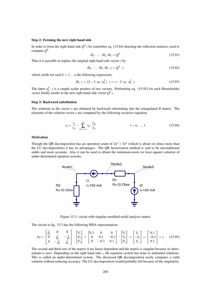
Step 2: Forming the new right hand side
In order to form the right hand side QT z let remember eq. (15.84) denoting the reflection matrices used tocompute QT .
Hn · . . . ·H2 ·H1 = QT (15.91)
Thus it is possible to replace the original right hand side vector z by
Hn · . . . ·H2 ·H1 ·z = QT ·z (15.92)
which yields for each k = 1 . . .n the following expression:
Hk ·z =(I−2 ·uk ·uT
k)·z = z−2 ·uk ·uT
k ·z (15.93)
The latter uTk ·z is a simple scalar product of two vectors. Performing eq. (15.93) for each Householder
vector finally results in the new right hand side vector QT z.
Step 3: Backward substitution
The solutions in the vector x are obtained by backward substituting into the triangulated R matrix. Theelements of the solution vector x are computed by the following recursive equation.
xi =zi
rii−
n
∑k=i+1
xk ·rik
riii = n, . . . ,1 (15.94)
Motivation
Though the QR decomposition has an operation count of 2n3 + 3n2 (which is about six times more thanthe LU decomposition) it has its advantages. The QR factorization method is said to be unconditionalstable and more accurate. Also it can be used to obtain the minimum-norm (or least square) solution ofunder-determined equation systems.
Figure 15.3: circuit with singular modified nodal analysis matrix
The circuit in fig. 15.3 has the following MNA representation:
Ax =
1
R20 0
0 1R1
− 1R1
0 − 1R1
1R1
·V1
V2V3
=
0.1 0 00 0.1 −0.10 −0.1 0.1
·V1
V2V3
=
I1−I1I2
=
0.1−0.10.1
= z (15.95)
The second and third row of the matrix A are linear dependent and the matrix is singular because its deter-minant is zero. Depending on the right hand side z, the equation system has none or unlimited solutions.This is called an under-determined system. The discussed QR decomposition easily computes a validsolution without reducing accuracy. The LU decomposition would probably fail because of the singularity.
205
QR decomposition with column pivoting
Least norm problem
With some more effort it is possible to obtain the minimum-norm solution of this problem. The algorithmas described here would probably yield the following solution:
x =
V1V2V3
=
101
(15.96)
This is one out of unlimited solutions. The following short description shows how it is possible to obtainthe minimum-norm solution. When decomposing the transposed problem
AT = Q ·R (15.97)
the minimum-norm solution x is obtained by forward substitution of
RT ·x = z (15.98)
and multiplying the result with Q.x = Q ·x (15.99)
In the example above this algorithm results in a solution vector with the least vector norm possible:
x =
V1V2V3
=
1−0.50.5
(15.100)
This algorithm outline is also sometimes called LQ decomposition because of RT being a lower triangularmatrix used by the forward substitution.
15.2.6 Singular value decompositionVery bad conditioned (ratio between largest and smallest eigenvalue) matrices, i.e. nearly singular, oreven singular matrices (over- or under-determined equation systems) can be handled by the singular valuedecomposition (SVD). This type of decomposition is defined by
A = U ·Σ ·V H (15.101)
where the U matrix consists of the orthonormalized eigenvectors associated with the eigenvalues of A ·AH ,V consists of the orthonormalized eigenvectors of AH ·A and Σ is a matrix with the singular values of A(non-negative square roots of the eigenvalues of AH ·A) on its diagonal and zeros otherwise.
Σ =
σ1 0 · · · 00 σ2 · · · 0...
.... . .
...0 0 · · · σn
(15.102)
The singular value decomposition can be used to solve linear equation systems by simple substitutions
A ·x = z (15.103)
U ·Σ ·V H ·x = z (15.104)
Σ ·V H ·x = UH ·z (15.105)
sinceUH ·U = V H ·V = V ·V H = I (15.106)
206
To obtain the decomposition stated in eq. (15.101) Householder vectors are computed and their transfor-mations are applied from the left-hand side and right-hand side to obtain an upper bidiagonal matrix Bwhich has the same singular values as the original A matrix because all of the transformations introducedare orthogonal.
UH (n)B · . . . ·UH (1)
B ·A ·V (1)B · . . . ·V
(n−2)B = UH
B ·A ·VB = B(0) (15.107)
Specifically, UH (i)B annihilates the subdiagonal elements in column i and V ( j)
B zeros out the appropriateelements in row j.
B(0) =
β1 δ2 0 · · · 00 β2 δ3 0 0... 0
. . . . . . 00 0 0 βn−1 δn0 0 0 0 βn
(15.108)
Afterwards an iterative process (which turns out to be a QR iteration) is used to transform the bidiagonalmatrix B into a diagonal form by applying successive Givens transformations (therefore orthogonal as well)to the bidiagonal matrix. This iteration is said to have cubic convergence and yields the final singular valuesof the matrix A.
B(0)→ B(1)→ . . .→ Σ (15.109)
B(k+1) =(
U (k))H·B(k) ·V (k) (15.110)
Each of the transformations applied to the bidiagonal matrix is also applied to the matrices UB and V HB
which finally yield the U and V H matrices after convergence.
So far for the algorithm outline. Without the very details the following sections briefly describe each partof the singular value decomposition.
Notation
Beforehand some notation marks are going to be defined.
• Conjugate transposed (or adjoint):
A→(AT )∗ = (A∗)T = AH
• Euclidean norm:
‖x‖=
√n
∑i=1
xi ·x∗1 =
√n
∑i=1|xi|2 =
√|x1|2 + · · ·+ |xn|2 =
√x ·xH
• Hermitian (or self adjoint):A = AH
whereas AH denotes the conjugate transposed matrix of A. In the real case the matrix A is then saidto be “symmetric”.
• Unitary:A ·AH = AH ·A = I
Real matrices A with this property are called “orthogonal”.
207
Householder reflector
A Householder matrix is an elementary unitary matrix that is Hermitian. Its fundamental use is their abilityto transform a vector x to a multiple of~e1, the first column of the identity matrix. The elementary Hermitian(i.e. the Householder matrix) is defined as
H = I−2 ·u ·uH where uH ·u = 1 (15.111)
Beside excellent numerical properties, their application demonstrates their efficiency. If A is a matrix, then
H ·A = A−2 ·u ·uH ·A (15.112)
= A−2 ·u ·(AH ·u
)H
and hence explicit formation and storage of H is not required. Also columns (or rows) can be transformedindividually exploiting the fact that uH ·A yields a scalar product for single columns or rows.
Specific case In order to reduce a 4×4 matrix A to upper triangular form successive Householder reflec-tors must be applied.
A =
a11 a12 a13 a14a21 a22 a23 a24a31 a32 a33 a34a41 a42 a43 a44
(15.113)
In the first step the diagonal element a11 gets replaced and its below elements get annihilated by the multi-plication with an appropriate Householder vector, also the remaining right-hand columns get modified.
u1 =
u11u21u31u41
H1 = I−2 ·u1 ·uH1 → A1 = H1 ·A =
β1 a(1)
12 a(1)13 a(1)
14
0 a(1)22 a(1)
23 a(1)24
0 a(1)32 a(1)
33 a(1)34
0 a(1)42 a(1)
43 a(1)44
(15.114)
This process must be repeated
u2 =
0
u22u32u42
H2 = I−2 ·u2 ·uH2 → A2 = H2 ·A1 =
β1 a(2)
12 a(2)13 a(2)
14
0 β2 a(2)23 a(2)
24
0 0 a(2)33 a(2)
34
0 0 a(2)43 a(2)
44
(15.115)
u3 =
00
u33u43
H3 = I−2 ·u3 ·uH3 → A3 = H3 ·A2 =
β1 a(3)
12 a(3)13 a(3)
14
0 β2 a(3)23 a(3)
24
0 0 β3 a(3)34
0 0 0 a(3)44
(15.116)
u4 =
000
u44
H4 = I−2 ·u4 ·uH4 → A4 = H4 ·A3 =
β1 a(4)
12 a(4)13 a(4)
14
0 β2 a(4)23 a(4)
24
0 0 β3 a(4)34
0 0 0 β4
(15.117)
until the matrix A contains an upper triangular matrix R. The matrix Q can be expressed as the the productof the Householder vectors. The performed operations deliver
HH4 ·HH
3 ·HH2 ·HH
1 ·A = QH ·A = R → A = Q ·R (15.118)
208
since Q is unitary. The matrix Q itself can be expressed in terms of Hi using the following transformation.
QH = HH4 ·HH
3 ·HH2 ·HH
1 (15.119)(QH)H =
(HH
4 ·HH3 ·HH
2 ·HH1)H
(15.120)Q = H1 ·H2 ·H3 ·H4 (15.121)
The eqn. (15.119)-(15.121) are necessary to be mentioned only in case Q is not Hermitian, but still unitary.Otherwise there is no difference computing Q or QH using the Householder vectors. No care must be takenin choosing forward or backward accumulation.
General case In the general case it is necessary to find an elementary unitary matrix
H = I− τ ·u ·uH (15.122)
that satisfies the following three conditions.
|τ|2 ·uH ·u = τ+ τ∗ = 2 ·Reτ , HH ·x = γ ·‖x‖·~e1 , |γ|= 1 (15.123)
When choosing the elements uii = 1 it is possible the store the Householder vectors as well as the uppertriangular matrix R in the same storage of the matrix A. The Householder matrices Hi can be completelyrestored from the Householder vectors.
A =
β1 a12 a13 a14u21 β2 a23 a24u31 u32 β3 a34u41 u42 u43 β4
(15.124)
There exist several approaches to meet the conditions expressed in eq. (15.123). For fewer computationaleffort it may be convenient to choose γ to be real valued. With the notation
HH ·x = HH ·
α
x2x3x4
=
β
000
(15.125)
one possibility is to define the following calculation rules.
ν = sign(Reα) ·‖x‖ (15.126)
τ =α+ν
ν(15.127)
γ =−1 (15.128)β = γ ·‖x‖=−‖x‖ → real valued (15.129)
u =x+ν ·~e1
α+ν→ uii = 1 (15.130)
These definitions yield a complex τ, thus H is no more Hermitian but still unitary.
H = I− τ ·u ·uH → HH = I− τ∗ ·u ·uH (15.131)
209
Givens rotation
A Givens rotation is a plane rotation matrix. Such a plane rotation matrix is an orthogonal matrix that isdifferent from the identity matrix only in four elements.
M =
1 0 · · · · · · 0
0. . .
...... 1
+c 0 · · · 0 +s0 1 0...
. . ....
0 1 0−s 0 · · · 0 +c
1...
.... . . 0
0 · · · · · · 0 1
(15.132)
The elements are usually chosen so that
R =[
c s−s c
]c = cosθ, s = sinθ → |c|2 + |s|2 = 1 (15.133)
The most common use of such a plane rotation is to choose c and s such that for a given a and b
R =[
c s−s c
]·[
ab
]=[
d0
](15.134)
multiplication annihilates the lower vector entry. In such an application the matrix R is often termed“Givens rotation” matrix. The following equations satisfy eq. (15.134) for a given a and b exploiting theconditions given in eq. (15.133).
c =±a√|a|2 + |b|2
and s =±b√|a|2 + |b|2
(15.135)
d =√|a|2 + |b|2 (15.136)
Eigenvalues of a 2-by-2 matrix
The eigenvalues of a 2-by-2 matrix
A =[
a bc d
](15.137)
can be obtained directly from the quadratic formula. The characteristic polynomial is
det (A−µI) = det[
a−µ bc d−µ
]= (a−µ) · (d−µ)−bc
0 = µ2− (a+d) ·µ+(ad−bc)(15.138)
The polynomial yields the two eigenvalues.
µ1,2 =a+d
2±
√(a+d
2
)2
+bc−ad (15.139)
For a symmetric matrix A (i.e. b = c) eq.(15.139) can be rewritten to:
µ1,2 = e+d±√
e2 +b2 with e =a−d
2(15.140)
210
Step 1: Bidiagonalization
In the first step the original matrix A is bidiagonalized by the application of Householder reflections fromthe left and right hand side. The matrices UH
B and VB can each be determined as a product of Householdermatrices.
UH (n)B · . . . ·UH (1)
B︸ ︷︷ ︸UH
B
·A ·V (1)B · . . . ·V
(n−2)B︸ ︷︷ ︸
VB
= UHB ·A ·VB = B(0) (15.141)
Each of the required Householder vectors are created and applied as previously defined. Suppose a n× nmatrix, then applying the first Householder vector from the left hand side eliminates the first column andyields
UH (1)B ·A =
β1 a(1)
12 a(1)13 · · · a(1)
1n
u21 a(1)22 a(1)
23 a(1)2n
u31 a(1)32 a(1)
33 a(1)3n
.... . .
...un1 a(1)
n2 a(1)n3 · · · a(1)
nn
(15.142)
Next, a Householder vector is applied from the right hand side to annihilate the first row.
UH (1)B ·A ·V (1)
B =
β1 δ2 v13 · · · v1n
u21 a(2)22 a(2)
23 a(2)2n
u31 a(2)32 a(2)
33 a(2)3n
.... . .
...un1 a(2)
n2 a(2)n3 · · · a(2)
nn
(15.143)
Again, a Householder vector is applied from the left hand side to annihilate the second column.
UH (2)B ·UH (1)
B ·A ·V (1)B =
β1 δ2 v13 · · · v1n
u21 β2 a(3)23 a(3)
2n
u31 u32 a(3)33 a(3)
3n...
.... . .
...un1 un2 a(3)
n3 · · · a(3)nn
(15.144)
This process is continued until
UHB ·A ·VB =
β1 δ2 v13 · · · v1nu21 β2 δ3 v2n
u31 u32. . . . . .
...... βn−1 δn
un1 un2 un3 βn
(15.145)
For each of the Householder transformations from the left and right hand side the appropriate τ values mustbe stored in separate vectors.
Step 2: Matrix reconstructions
Using the Householder vectors stored in place of the original A matrix and the appropriate τ value vectorsit is now necessary to unpack the UB and V H
B matrices. The diagonal vector β and the super-diagonal vectorδ can be saved in separate vectors previously. Thus the UB matrix can be unpacked in place of the A matrixand the V H
B matrix is unpacked in a separate matrix.
211
There are two possible algorithms for computing the Householder product matrices, i.e. forward accumu-lation and backward accumulation. Both start with the identity matrix which is successively multiplied bythe Householder matrices either from the left or right.
UHB = HH
Un · . . . ·HHU2 ·HH
U1 · I (15.146)→ UB = I ·HUn · . . . ·HU2 ·HU1 (15.147)
Recall that the leading portion of each Householder matrix is the identity except the first. Thus, at thebeginning of backward accumulation, UB is “mostly the identity” and it gradually becomes full as theiteration progresses. This pattern can be exploited to reduce the number of required flops. In contrast, UH
Bis full in forward accumulation after the first step. For this reason, backward accumulation is cheaper andthe strategy of choice. When unpacking the UB matrix in place of the original A matrix it is necessary tochoose backward accumulation anyway.
VB = I ·HHV 1 ·HH
V 2 · . . . ·HHV n (15.148)
→ V HB = I ·HV n · . . . ·HV 2 ·HV 1 (15.149)
Unpacking the V HB matrix is done in a similar way also performing successive Householder matrix multi-
plications using backward accumulation.
Step 3: Diagonalization – shifted QR iteration
At this stage the matrices UB and V HB exist in unfactored form. Also there are the diagonal vector β and the
super-diagonal vector δ. Both vectors are real valued. Thus the following algorithm can be applied eventhough solving a complex equation system.
B(0) =
β1 δ2 0 · · · 00 β2 δ3 0 0... 0
. . . . . . 00 0 0 βn−1 δn0 0 0 0 βn
(15.150)
The remaining problem is thus to compute the SVD of the matrix B. This is done applying an implicit-shiftQR step to the tridiagonal matrix T = BT B which is a symmetric. The matrix T is not explicitly formedthat is why a QR iteration with implicit shifts is applied.
After bidiagonalization we have a bidiagonal matrix B(0):
B(0) = UHB ·A ·VB (15.151)
The presented method turns B(k) into a matrix B(k+1) by applying a set of orthogonal transforms
B(k+1) = UH ·B(k) ·V (15.152)
The orthogonal matrices U and V are chosen so that B(k+1) is also a bidiagonal matrix, but with the super-diagonal elements smaller than those of B(k). The eq.(15.152) is repeated until the non-diagonal elementsof B(k+1) become smaller than ε and can be disregarded.
The matrices U and V are constructed as
U = U1 ·U2 ·U3 · . . . ·Un−1 (15.153)
and similarly V where Vi and Ui are matrices of simple rotations as given in eq.(15.132). Both V and U areproducts of Givens rotations and thus perform orthogonal transforms.
212
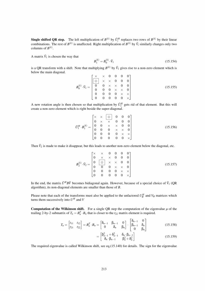
Single shifted QR step. The left multiplication of B(k) by UHi replaces two rows of B(k) by their linear
combinations. The rest of B(k) is unaffected. Right multiplication of B(k) by Vi similarly changes only twocolumns of B(k).
A matrix V1 is chosen the way thatB(k)
1 = B(k)0 ·V1 (15.154)
is a QR transform with a shift. Note that multiplying B(k) by V1 gives rise to a non-zero element which isbelow the main diagonal.
B(k)0 ·V1 =
× × 0 0 0 0⊗ × × 0 0 00 0 × × 0 00 0 0 × × 00 0 0 0 × ×0 0 0 0 0 ×
(15.155)
A new rotation angle is then chosen so that multiplication by UH1 gets rid of that element. But this will
create a non-zero element which is right beside the super-diagonal.
UH1 ·B
(k)1 =
× × ⊗ 0 0 00 × × 0 0 00 0 × × 0 00 0 0 × × 00 0 0 0 × ×0 0 0 0 0 ×
(15.156)
Then V2 is made to make it disappear, but this leads to another non-zero element below the diagonal, etc.
B(k)2 ·V2 =
× × 0 0 0 00 × × 0 0 00 ⊗ × × 0 00 0 0 × × 00 0 0 0 × ×0 0 0 0 0 ×
(15.157)
In the end, the matrix UHBV becomes bidiagonal again. However, because of a special choice of V1 (QRalgorithm), its non-diagonal elements are smaller than those of B.
Please note that each of the transforms must also be applied to the unfactored UHB and VB matrices which
turns them successively into UH and V
Computation of the Wilkinson shift. For a single QR step the computation of the eigenvalue µ of thetrailing 2-by-2 submatrix of Tn = BT
n ·Bn that is closer to the t22 matrix element is required.
Tn =[
t11 t12t21 t22
]= BT
n ·Bn =[
δn−1 βn−1 00 δn βn
]·
δn−1 0βn−1 δn
0 βn
(15.158)
=[
β2n−1 +δ2
n−1 δn ·βn−1δn ·βn−1 β2
n +δ2n
](15.159)
The required eigenvalue is called Wilkinson shift, see eq.(15.140) for details. The sign for the eigenvalue
213
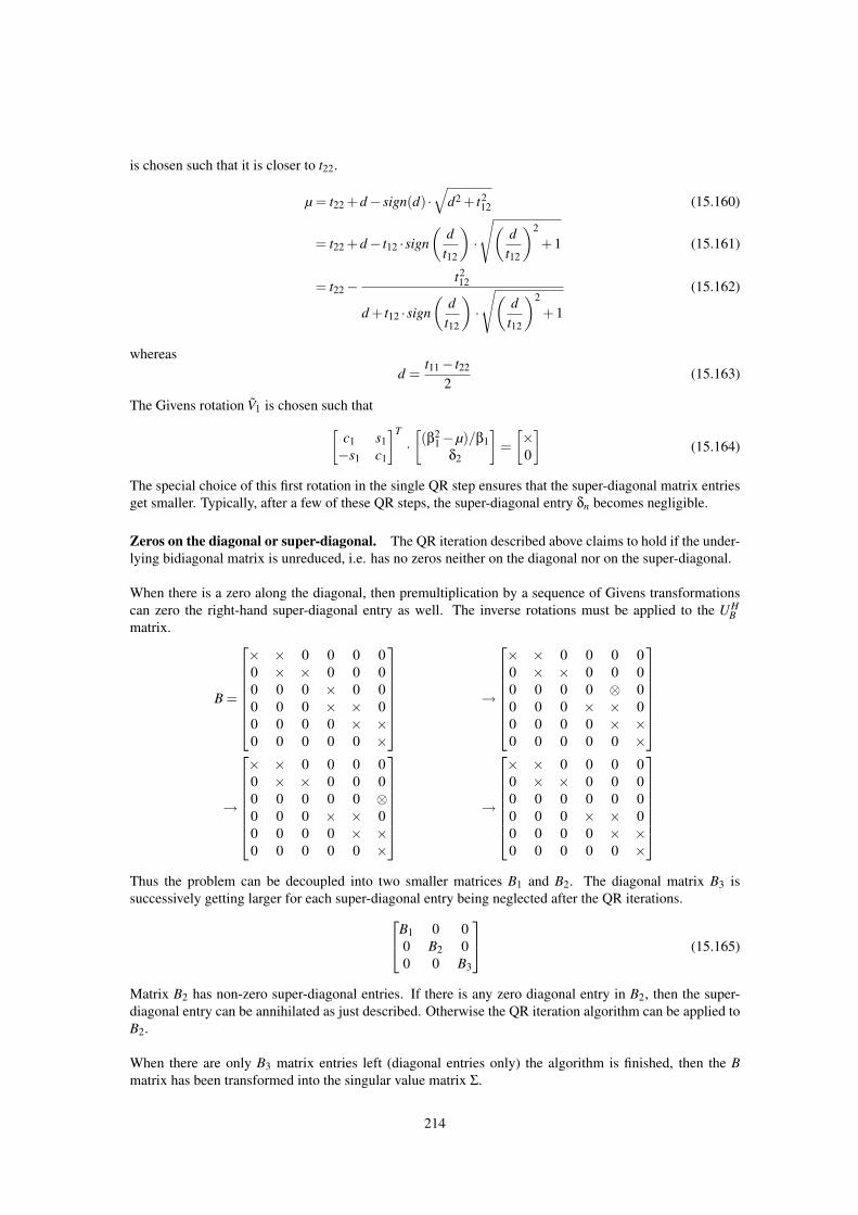
is chosen such that it is closer to t22.
µ = t22 +d− sign(d) ·√
d2 + t212 (15.160)
= t22 +d− t12 ·sign(
dt12
)·
√(d
t12
)2
+1 (15.161)
= t22−t212
d + t12 ·sign(
dt12
)·
√(d
t12
)2
+1
(15.162)
whereasd =
t11− t22
2(15.163)
The Givens rotation V1 is chosen such that[c1 s1−s1 c1
]T
·[(β2
1−µ)/β1δ2
]=[×0
](15.164)
The special choice of this first rotation in the single QR step ensures that the super-diagonal matrix entriesget smaller. Typically, after a few of these QR steps, the super-diagonal entry δn becomes negligible.
Zeros on the diagonal or super-diagonal. The QR iteration described above claims to hold if the under-lying bidiagonal matrix is unreduced, i.e. has no zeros neither on the diagonal nor on the super-diagonal.
When there is a zero along the diagonal, then premultiplication by a sequence of Givens transformationscan zero the right-hand super-diagonal entry as well. The inverse rotations must be applied to the UH
Bmatrix.
B =
× × 0 0 0 00 × × 0 0 00 0 0 × 0 00 0 0 × × 00 0 0 0 × ×0 0 0 0 0 ×
→
× × 0 0 0 00 × × 0 0 00 0 0 0 ⊗ 00 0 0 × × 00 0 0 0 × ×0 0 0 0 0 ×
→
× × 0 0 0 00 × × 0 0 00 0 0 0 0 ⊗0 0 0 × × 00 0 0 0 × ×0 0 0 0 0 ×
→
× × 0 0 0 00 × × 0 0 00 0 0 0 0 00 0 0 × × 00 0 0 0 × ×0 0 0 0 0 ×
Thus the problem can be decoupled into two smaller matrices B1 and B2. The diagonal matrix B3 issuccessively getting larger for each super-diagonal entry being neglected after the QR iterations.B1 0 0
0 B2 00 0 B3
(15.165)
Matrix B2 has non-zero super-diagonal entries. If there is any zero diagonal entry in B2, then the super-diagonal entry can be annihilated as just described. Otherwise the QR iteration algorithm can be applied toB2.
When there are only B3 matrix entries left (diagonal entries only) the algorithm is finished, then the Bmatrix has been transformed into the singular value matrix Σ.
214
Step 4: Solving the equation system
It is straight-forward to solve a given equation system once having the singular value decomposition com-puted.
A ·x = z (15.166)
UΣV H ·x = z (15.167)
ΣV H ·x = UH ·z (15.168)
V H ·x = Σ−1UH ·z (15.169)
x = V Σ−1UH ·z (15.170)
The inverse of the diagonal matrix Σ yields
Σ−1 =
1/σ1 0 · · · 0
0 1/σ2 · · · 0...
.... . .
...0 0 · · · 1/σn
(15.171)
With vi being the i-th row of the matrix V , ui the i-th column of the matrix U and σi the i-th singular valueeq. (15.170) can be rewritten to
x =n
∑i=1
uHi ·zσi·vi (15.172)
It must be mentioned that very small singular values σi corrupt the complete result. Such values indicate(nearly) singular (ill-conditioned) matrices A. In such cases, the solution vector x obtained by zeroing thesmall σi’s and then using equation (15.170) is better than direct-method solutions (such as LU decompo-sition or Gaussian elimination) and the SVD solution where the small σi’s are left non-zero. It may seemparadoxical that this can be so, since zeroing a singular value corresponds to throwing away one linearcombination of the set of equations that is going to be solved. The resolution of the paradox is that acombination of equations that is so corrupted by roundoff error is thrown away precisely as to be at bestuseless; usually it is worse than useless since it ”pulls” the solution vector way off towards infinity alongsome direction that is almost a nullspace vector.
15.2.7 Jacobi methodThis method quite simply involves rearranging each equation to make each variable a function of the othervariables. Then make an initial guess for each solution and iterate. For this method it is necessary to ensurethat all the diagonal matrix elements aii are non-zero. This is given for the nodal analysis and almostlygiven for the modified nodal analysis. If the linear equation system is solvable this can always be achievedby rows substitutions.
The algorithm for performing the iteration step k +1 writes as follows.
x(k+1)i =
1aii
(zi−
i−1
∑j=1
ai jx(k)j −
n
∑j=i+1
ai jx(k)j
)for i = 1, . . . ,n (15.173)
This has to repeated until the new solution vectors x(k+1) deviation from the previous one x(k) is sufficientlysmall.
The initial guess has no effect on whether the iterative method converges or not, but with a good initialguess (as possibly given in consecutive Newton-Raphson iterations) it converges faster (if it converges). Toensure convergence the condition
n
∑j=1, j 6=i
∣∣ai j∣∣≤ |aii| for i = 1, . . . ,n (15.174)
215
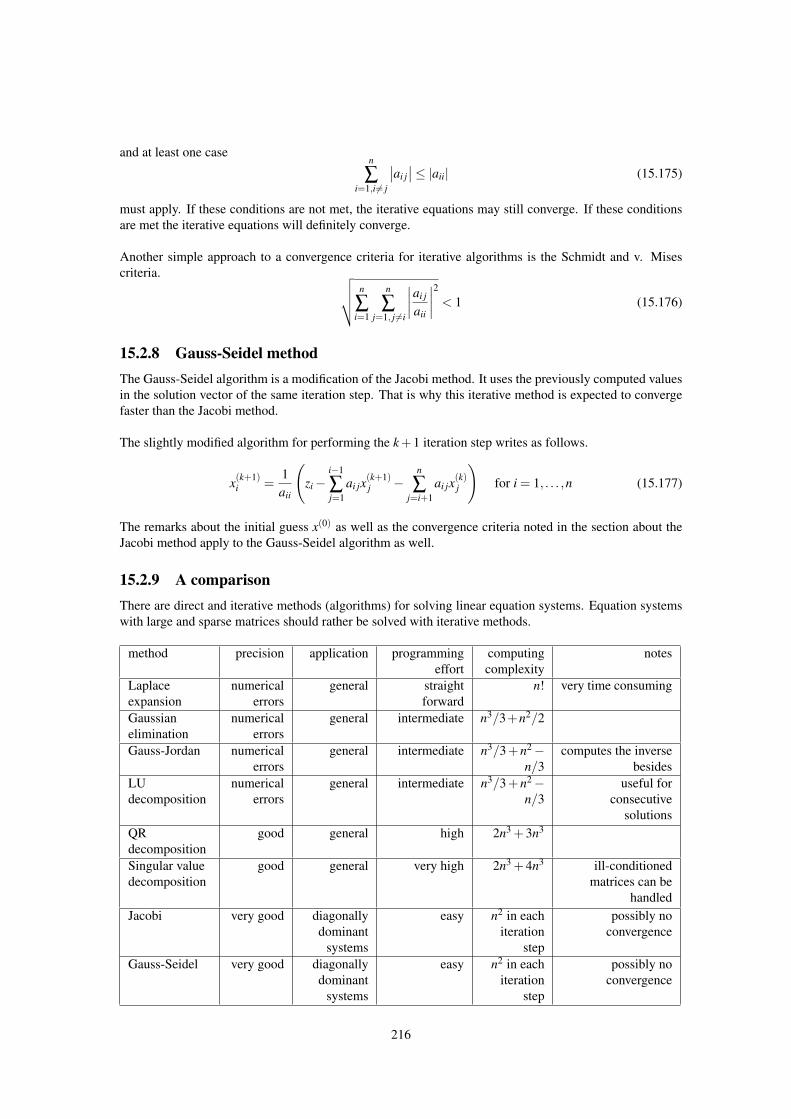
and at least one casen
∑i=1,i6= j
∣∣ai j∣∣≤ |aii| (15.175)
must apply. If these conditions are not met, the iterative equations may still converge. If these conditionsare met the iterative equations will definitely converge.
Another simple approach to a convergence criteria for iterative algorithms is the Schmidt and v. Misescriteria. √√√√ n
∑i=1
n
∑j=1, j 6=i
∣∣∣∣ai j
aii
∣∣∣∣2 < 1 (15.176)
15.2.8 Gauss-Seidel methodThe Gauss-Seidel algorithm is a modification of the Jacobi method. It uses the previously computed valuesin the solution vector of the same iteration step. That is why this iterative method is expected to convergefaster than the Jacobi method.
The slightly modified algorithm for performing the k +1 iteration step writes as follows.
x(k+1)i =
1aii
(zi−
i−1
∑j=1
ai jx(k+1)j −
n
∑j=i+1
ai jx(k)j
)for i = 1, . . . ,n (15.177)
The remarks about the initial guess x(0) as well as the convergence criteria noted in the section about theJacobi method apply to the Gauss-Seidel algorithm as well.
15.2.9 A comparisonThere are direct and iterative methods (algorithms) for solving linear equation systems. Equation systemswith large and sparse matrices should rather be solved with iterative methods.
method precision application programmingeffort
computingcomplexity
notes
Laplaceexpansion
numericalerrors
general straightforward
n! very time consuming
Gaussianelimination
numericalerrors
general intermediate n3/3+n2/2
Gauss-Jordan numericalerrors
general intermediate n3/3+n2−n/3
computes the inversebesides
LUdecomposition
numericalerrors
general intermediate n3/3+n2−n/3
useful forconsecutive
solutionsQRdecomposition
good general high 2n3 +3n3
Singular valuedecomposition
good general very high 2n3 +4n3 ill-conditionedmatrices can be
handledJacobi very good diagonally
dominantsystems
easy n2 in eachiteration
step
possibly noconvergence
Gauss-Seidel very good diagonallydominant
systems
easy n2 in eachiteration
step
possibly noconvergence
216
15.3 Polynomial approximations
15.3.1 Cubic splines
15.4 Frequency-Time Domain TransformationAny signal can completely be described in time or in frequency domain. As both representations are equiv-alent, it is possible to transform them into each other. This is done by the so-called Fourier Transformationand the inverse Fourier Transformation, respectively:
Fourier Transformation: U( jω) =∞Z−∞
u(t) ·e− jω· t dt (15.178)
inverse Fourier Transformation: u(t) =1
2π·
∞Z−∞
U( jω) ·e jω· t dω (15.179)
In digital systems the data u(t) or U( jω), respectively, consists of a finite number N of samples uk and Un.This leads to the discrete Fourier Transformation (DFT) and its inverse operation (IDFT):
DFT: Un =N−1
∑k=0
uk · exp(− j ·n2π ·k
N
)(15.180)
IDFT: uk =1N·
N
∑n=0
Un · exp(
j ·k 2π ·nN
)(15.181)
The absolute time and frequency values do not appear anymore in the DFT. They depend on the samplefrequency fT and the number of samples N.
∆ f =1
N ·∆t=
fT
N(15.182)
Where ∆t is distance between time samples and ∆ f distance between frequency samples.
With DFT the N time samples are transformed into N frequency samples. This also holds if the timedata are real numbers, as is always the case in ”real life”: The complex frequency samples are conjugatecomplex symmetrical and so equalizing the score:
UN−n = U∗n (15.183)
That is, knowing the input data has no imaginary part, only half of the Fourier data must be computed.
15.4.1 Fast Fourier TransformationAs can be seen in equation 15.180 the computing time of the DFT rises with N2. This is really huge, so itis very important to reduce the time consumption. Using a strongly optimized algorithm, the so-called FastFourier Transformation (FFT), the DFT is reduced to an N · log2 N time rise. The following informationstems from [61], where the theoretical background is explained comprehensively.
The fundamental trick of the FFT is to cut the DFT into two parts, one with data having even indices andthe other with odd indices:
217
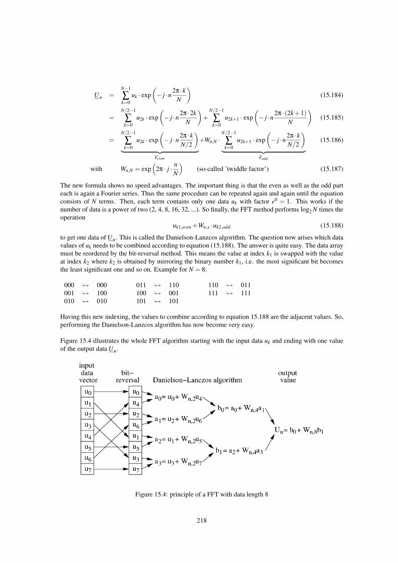
Un =N−1
∑k=0
uk · exp(− j ·n2π ·k
N
)(15.184)
=N/2−1
∑k=0
u2k · exp(− j ·n2π ·2k
N
)+
N/2−1
∑k=0
u2k+1 · exp(− j ·n2π ·(2k +1)
N
)(15.185)
=N/2−1
∑k=0
u2k · exp(− j ·n2π ·k
N/2
)︸ ︷︷ ︸
Feven
+Wn,N ·N/2−1
∑k=0
u2k+1 · exp(− j ·n2π ·k
N/2
)︸ ︷︷ ︸
Fodd
(15.186)
with Wn,N = exp(
2π · j · nN
)(so-called ’twiddle factor’) (15.187)
The new formula shows no speed advantages. The important thing is that the even as well as the odd parteach is again a Fourier series. Thus the same procedure can be repeated again and again until the equationconsists of N terms. Then, each term contains only one data uk with factor e0 = 1. This works if thenumber of data is a power of two (2, 4, 8, 16, 32, ...). So finally, the FFT method performs log2 N times theoperation
uk1,even +Wn,x ·uk2,odd (15.188)
to get one data of Un. This is called the Danielson-Lanzcos algorithm. The question now arises which datavalues of uk needs to be combined according to equation (15.188). The answer is quite easy. The data arraymust be reordered by the bit-reversal method. This means the value at index k1 is swapped with the valueat index k2 where k2 is obtained by mirroring the binary number k1, i.e. the most significant bit becomesthe least significant one and so on. Example for N = 8:
000 ↔ 000 011 ↔ 110 110 ↔ 011001 ↔ 100 100 ↔ 001 111 ↔ 111010 ↔ 010 101 ↔ 101
Having this new indexing, the values to combine according to equation 15.188 are the adjacent values. So,performing the Danielson-Lanzcos algorithm has now become very easy.
Figure 15.4 illustrates the whole FFT algorithm starting with the input data uk and ending with one valueof the output data Un.
Figure 15.4: principle of a FFT with data length 8
218
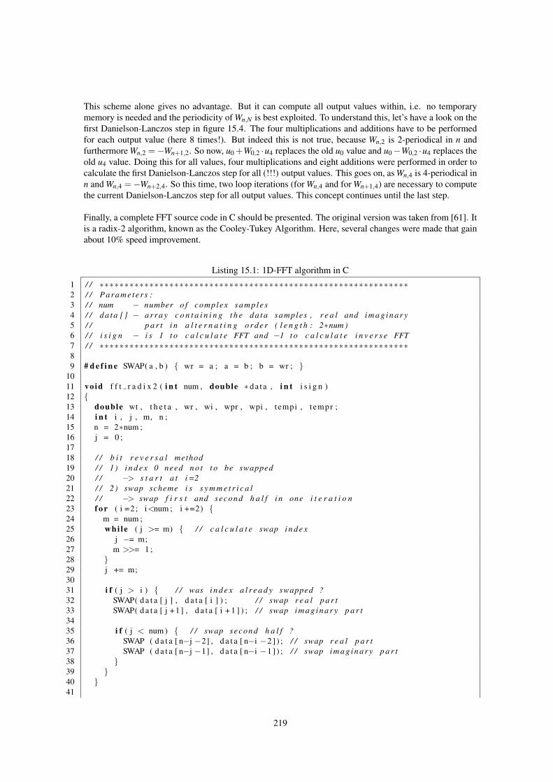
This scheme alone gives no advantage. But it can compute all output values within, i.e. no temporarymemory is needed and the periodicity of Wn,N is best exploited. To understand this, let’s have a look on thefirst Danielson-Lanczos step in figure 15.4. The four multiplications and additions have to be performedfor each output value (here 8 times!). But indeed this is not true, because Wn,2 is 2-periodical in n andfurthermore Wn,2 =−Wn+1,2. So now, u0 +W0,2 ·u4 replaces the old u0 value and u0−W0,2 ·u4 replaces theold u4 value. Doing this for all values, four multiplications and eight additions were performed in order tocalculate the first Danielson-Lanczos step for all (!!!) output values. This goes on, as Wn,4 is 4-periodical inn and Wn,4 =−Wn+2,4. So this time, two loop iterations (for Wn,4 and for Wn+1,4) are necessary to computethe current Danielson-Lanczos step for all output values. This concept continues until the last step.
Finally, a complete FFT source code in C should be presented. The original version was taken from [61]. Itis a radix-2 algorithm, known as the Cooley-Tukey Algorithm. Here, several changes were made that gainabout 10% speed improvement.
Listing 15.1: 1D-FFT algorithm in C
1 / / ∗∗∗∗∗∗∗∗∗∗∗∗∗∗∗∗∗∗∗∗∗∗∗∗∗∗∗∗∗∗∗∗∗∗∗∗∗∗∗∗∗∗∗∗∗∗∗∗∗∗∗∗∗∗∗∗∗∗∗∗∗∗2 / / Parame ter s :3 / / num − number o f complex samples4 / / da ta [ ] − a r r a y c o n t a i n i n g t h e da ta samples , r e a l and i m a g i n a r y5 / / p a r t i n a l t e r n a t i n g o r d e r ( l e n g t h : 2∗num )6 / / i s i g n − i s 1 t o c a l c u l a t e FFT and −1 t o c a l c u l a t e i n v e r s e FFT7 / / ∗∗∗∗∗∗∗∗∗∗∗∗∗∗∗∗∗∗∗∗∗∗∗∗∗∗∗∗∗∗∗∗∗∗∗∗∗∗∗∗∗∗∗∗∗∗∗∗∗∗∗∗∗∗∗∗∗∗∗∗∗∗89 # d e f i n e SWAP( a , b ) wr = a ; a = b ; b = wr ;
1011 void f f t r a d i x 2 ( i n t num , double ∗ da ta , i n t i s i g n )12 13 double wt , t h e t a , wr , wi , wpr , wpi , tempi , tempr ;14 i n t i , j , m, n ;15 n = 2∗num ;16 j = 0 ;1718 / / b i t r e v e r s a l method19 / / 1 ) i n d e x 0 need n o t t o be swapped20 / / −> s t a r t a t i =221 / / 2 ) swap scheme i s s y m m e t r i c a l22 / / −> swap f i r s t and second h a l f i n one i t e r a t i o n23 f o r ( i =2 ; i<num ; i +=2) 24 m = num ;25 whi le ( j >= m) / / c a l c u l a t e swap i n d e x26 j −= m;27 m >>= 1 ;28 29 j += m;3031 i f ( j > i ) / / was i n d e x a l r e a d y swapped ?32 SWAP( d a t a [ j ] , d a t a [ i ] ) ; / / swap r e a l p a r t33 SWAP( d a t a [ j +1 ] , d a t a [ i + 1 ] ) ; / / swap i m a g i n a r y p a r t3435 i f ( j < num ) / / swap second h a l f ?36 SWAP ( d a t a [ n−j −2] , d a t a [ n−i −2 ] ) ; / / swap r e a l p a r t37 SWAP ( d a t a [ n−j −1] , d a t a [ n−i −1 ] ) ; / / swap i m a g i n a r y p a r t38 39 40 41
219
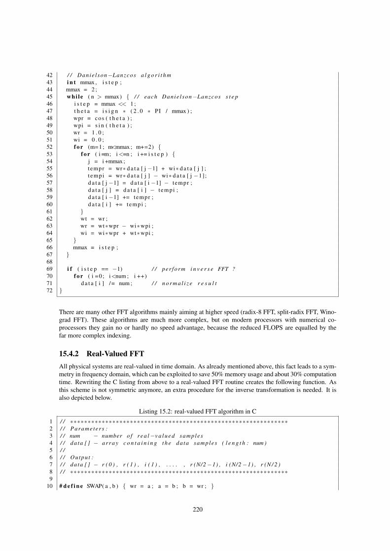
42 / / Dan ie l son−Lanzcos a l g o r i t h m43 i n t mmax , i s t e p ;44 mmax = 2 ;45 whi le ( n > mmax) / / each Danie l son−Lanzcos s t e p46 i s t e p = mmax << 1 ;47 t h e t a = i s i g n ∗ ( 2 . 0 ∗ PI / mmax ) ;48 wpr = cos ( t h e t a ) ;49 wpi = s i n ( t h e t a ) ;50 wr = 1 . 0 ;51 wi = 0 . 0 ;52 f o r (m=1; m<mmax ; m+=2) 53 f o r ( i =m; i <=n ; i += i s t e p ) 54 j = i +mmax ;55 tempr = wr∗ d a t a [ j −1] + wi∗ d a t a [ j ] ;56 tempi = wr∗ d a t a [ j ] − wi∗ d a t a [ j −1];57 d a t a [ j −1] = d a t a [ i −1] − t empr ;58 d a t a [ j ] = d a t a [ i ] − t empi ;59 d a t a [ i −1] += tempr ;60 d a t a [ i ] += tempi ;61 62 wt = wr ;63 wr = wt∗wpr − wi∗wpi ;64 wi = wi∗wpr + wt∗wpi ;65 66 mmax = i s t e p ;67 6869 i f ( i s t e p == −1) / / pe r fo rm i n v e r s e FFT ?70 f o r ( i =0 ; i<num ; i ++)71 d a t a [ i ] /= num ; / / n o r m a l i z e r e s u l t72
There are many other FFT algorithms mainly aiming at higher speed (radix-8 FFT, split-radix FFT, Wino-grad FFT). These algorithms are much more complex, but on modern processors with numerical co-processors they gain no or hardly no speed advantage, because the reduced FLOPS are equalled by thefar more complex indexing.
15.4.2 Real-Valued FFTAll physical systems are real-valued in time domain. As already mentioned above, this fact leads to a sym-metry in frequency domain, which can be exploited to save 50% memory usage and about 30% computationtime. Rewriting the C listing from above to a real-valued FFT routine creates the following function. Asthis scheme is not symmetric anymore, an extra procedure for the inverse transformation is needed. It isalso depicted below.
Listing 15.2: real-valued FFT algorithm in C
1 / / ∗∗∗∗∗∗∗∗∗∗∗∗∗∗∗∗∗∗∗∗∗∗∗∗∗∗∗∗∗∗∗∗∗∗∗∗∗∗∗∗∗∗∗∗∗∗∗∗∗∗∗∗∗∗∗∗∗∗∗∗∗∗2 / / Parame ter s :3 / / num − number o f r e a l−v a l u e d samples4 / / da ta [ ] − a r r a y c o n t a i n i n g t h e da ta samples ( l e n g t h : num )5 / /6 / / Ou tpu t :7 / / da ta [ ] − r ( 0 ) , r ( 1 ) , i ( 1 ) , . . . . , r (N/2−1) , i (N/2−1) , r (N / 2 )8 / / ∗∗∗∗∗∗∗∗∗∗∗∗∗∗∗∗∗∗∗∗∗∗∗∗∗∗∗∗∗∗∗∗∗∗∗∗∗∗∗∗∗∗∗∗∗∗∗∗∗∗∗∗∗∗∗∗∗∗∗∗∗∗9
10 # d e f i n e SWAP( a , b ) wr = a ; a = b ; b = wr ;
220
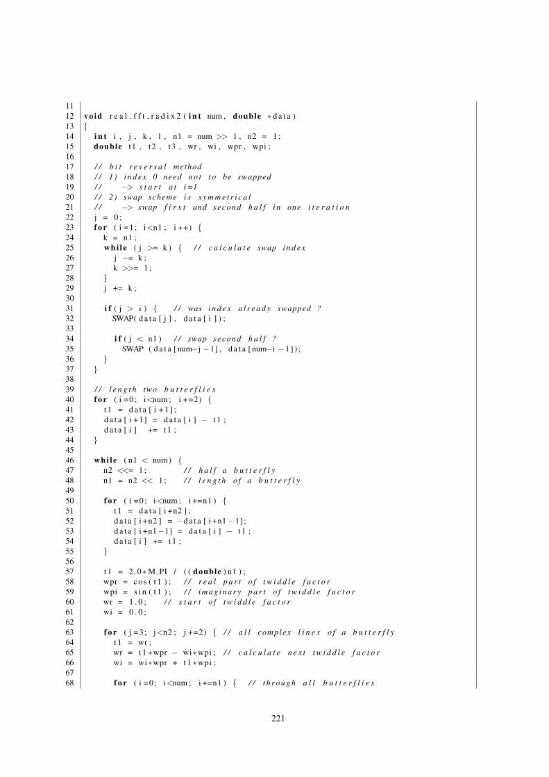
1112 void r e a l f f t r a d i x 2 ( i n t num , double ∗ d a t a )13 14 i n t i , j , k , l , n1 = num >> 1 , n2 = 1 ;15 double t1 , t2 , t3 , wr , wi , wpr , wpi ;1617 / / b i t r e v e r s a l method18 / / 1 ) i n d e x 0 need n o t t o be swapped19 / / −> s t a r t a t i =120 / / 2 ) swap scheme i s s y m m e t r i c a l21 / / −> swap f i r s t and second h a l f i n one i t e r a t i o n22 j = 0 ;23 f o r ( i =1 ; i<n1 ; i ++) 24 k = n1 ;25 whi le ( j >= k ) / / c a l c u l a t e swap i n d e x26 j −= k ;27 k >>= 1 ;28 29 j += k ;3031 i f ( j > i ) / / was i n d e x a l r e a d y swapped ?32 SWAP( d a t a [ j ] , d a t a [ i ] ) ;3334 i f ( j < n1 ) / / swap second h a l f ?35 SWAP ( d a t a [ num−j −1] , d a t a [ num−i −1 ] ) ;36 37 3839 / / l e n g t h two b u t t e r f l i e s40 f o r ( i =0 ; i<num ; i +=2) 41 t 1 = d a t a [ i + 1 ] ;42 d a t a [ i +1] = d a t a [ i ] − t 1 ;43 d a t a [ i ] += t 1 ;44 4546 whi le ( n1 < num ) 47 n2 <<= 1 ; / / h a l f a b u t t e r f l y48 n1 = n2 << 1 ; / / l e n g t h o f a b u t t e r f l y4950 f o r ( i =0 ; i<num ; i +=n1 ) 51 t 1 = d a t a [ i +n2 ] ;52 d a t a [ i +n2 ] = −d a t a [ i +n1−1];53 d a t a [ i +n1−1] = d a t a [ i ] − t 1 ;54 d a t a [ i ] += t 1 ;55 5657 t 1 = 2 . 0∗M PI / ( ( double ) n1 ) ;58 wpr = cos ( t 1 ) ; / / r e a l p a r t o f t w i d d l e f a c t o r59 wpi = s i n ( t 1 ) ; / / i m a g i n a r y p a r t o f t w i d d l e f a c t o r60 wr = 1 . 0 ; / / s t a r t o f t w i d d l e f a c t o r61 wi = 0 . 0 ;6263 f o r ( j =3 ; j<n2 ; j +=2) / / a l l complex l i n e s o f a b u t t e r f l y64 t 1 = wr ;65 wr = t 1 ∗wpr − wi∗wpi ; / / c a l c u l a t e n e x t t w i d d l e f a c t o r66 wi = wi∗wpr + t 1 ∗wpi ;6768 f o r ( i =0 ; i<num ; i +=n1 ) / / t h r o u g h a l l b u t t e r f l i e s
221
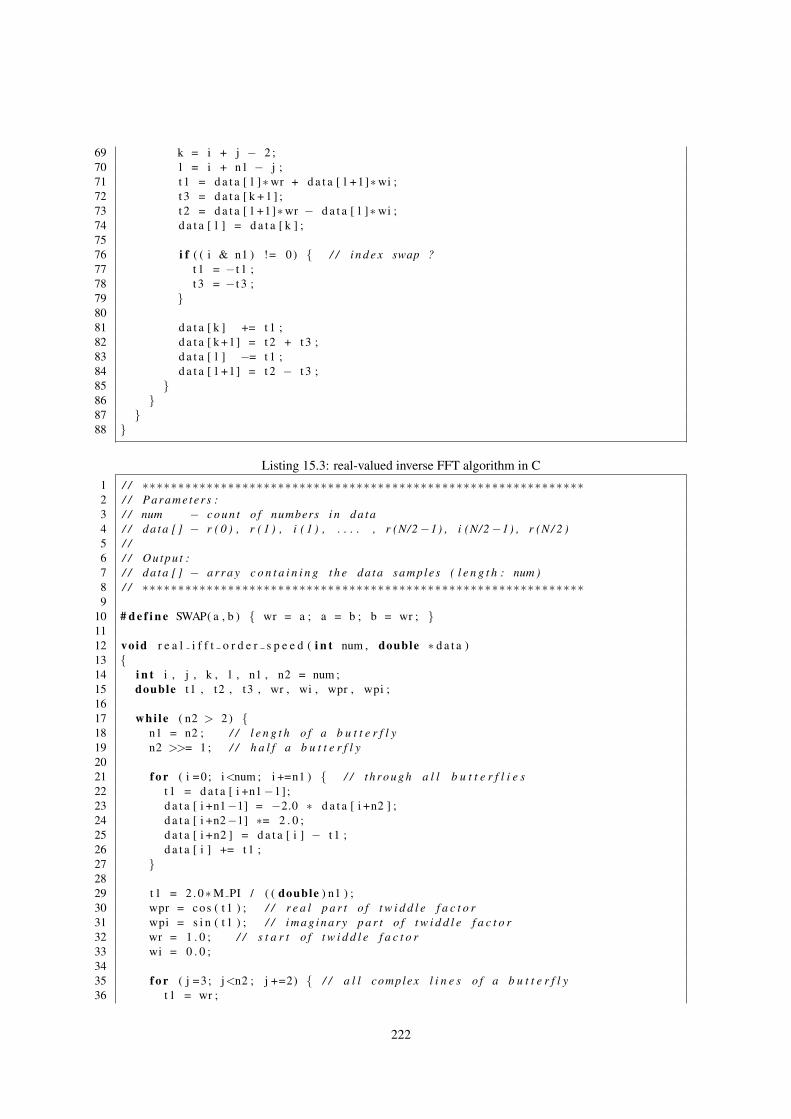
69 k = i + j − 2 ;70 l = i + n1 − j ;71 t 1 = d a t a [ l ]∗wr + d a t a [ l +1]∗wi ;72 t 3 = d a t a [ k + 1 ] ;73 t 2 = d a t a [ l +1]∗wr − d a t a [ l ]∗wi ;74 d a t a [ l ] = d a t a [ k ] ;7576 i f ( ( i & n1 ) != 0 ) / / i n d e x swap ?77 t 1 = −t 1 ;78 t 3 = −t 3 ;79 8081 d a t a [ k ] += t 1 ;82 d a t a [ k +1] = t 2 + t 3 ;83 d a t a [ l ] −= t 1 ;84 d a t a [ l +1] = t 2 − t 3 ;85 86 87 88
Listing 15.3: real-valued inverse FFT algorithm in C1 / / ∗∗∗∗∗∗∗∗∗∗∗∗∗∗∗∗∗∗∗∗∗∗∗∗∗∗∗∗∗∗∗∗∗∗∗∗∗∗∗∗∗∗∗∗∗∗∗∗∗∗∗∗∗∗∗∗∗∗∗∗∗∗2 / / Parame ter s :3 / / num − c o u n t o f numbers i n da ta4 / / da ta [ ] − r ( 0 ) , r ( 1 ) , i ( 1 ) , . . . . , r (N/2−1) , i (N/2−1) , r (N / 2 )5 / /6 / / Ou tpu t :7 / / da ta [ ] − a r r a y c o n t a i n i n g t h e da ta samples ( l e n g t h : num )8 / / ∗∗∗∗∗∗∗∗∗∗∗∗∗∗∗∗∗∗∗∗∗∗∗∗∗∗∗∗∗∗∗∗∗∗∗∗∗∗∗∗∗∗∗∗∗∗∗∗∗∗∗∗∗∗∗∗∗∗∗∗∗∗9
10 # d e f i n e SWAP( a , b ) wr = a ; a = b ; b = wr ; 1112 void r e a l i f f t o r d e r s p e e d ( i n t num , double ∗ d a t a )13 14 i n t i , j , k , l , n1 , n2 = num ;15 double t1 , t2 , t3 , wr , wi , wpr , wpi ;1617 whi le ( n2 > 2) 18 n1 = n2 ; / / l e n g t h o f a b u t t e r f l y19 n2 >>= 1 ; / / h a l f a b u t t e r f l y2021 f o r ( i =0 ; i<num ; i +=n1 ) / / t h r o u g h a l l b u t t e r f l i e s22 t 1 = d a t a [ i +n1−1];23 d a t a [ i +n1−1] = −2.0 ∗ d a t a [ i +n2 ] ;24 d a t a [ i +n2−1] ∗= 2 . 0 ;25 d a t a [ i +n2 ] = d a t a [ i ] − t 1 ;26 d a t a [ i ] += t 1 ;27 2829 t 1 = 2 . 0∗M PI / ( ( double ) n1 ) ;30 wpr = cos ( t 1 ) ; / / r e a l p a r t o f t w i d d l e f a c t o r31 wpi = s i n ( t 1 ) ; / / i m a g i n a r y p a r t o f t w i d d l e f a c t o r32 wr = 1 . 0 ; / / s t a r t o f t w i d d l e f a c t o r33 wi = 0 . 0 ;3435 f o r ( j =3 ; j<n2 ; j +=2) / / a l l complex l i n e s o f a b u t t e r f l y36 t 1 = wr ;
222
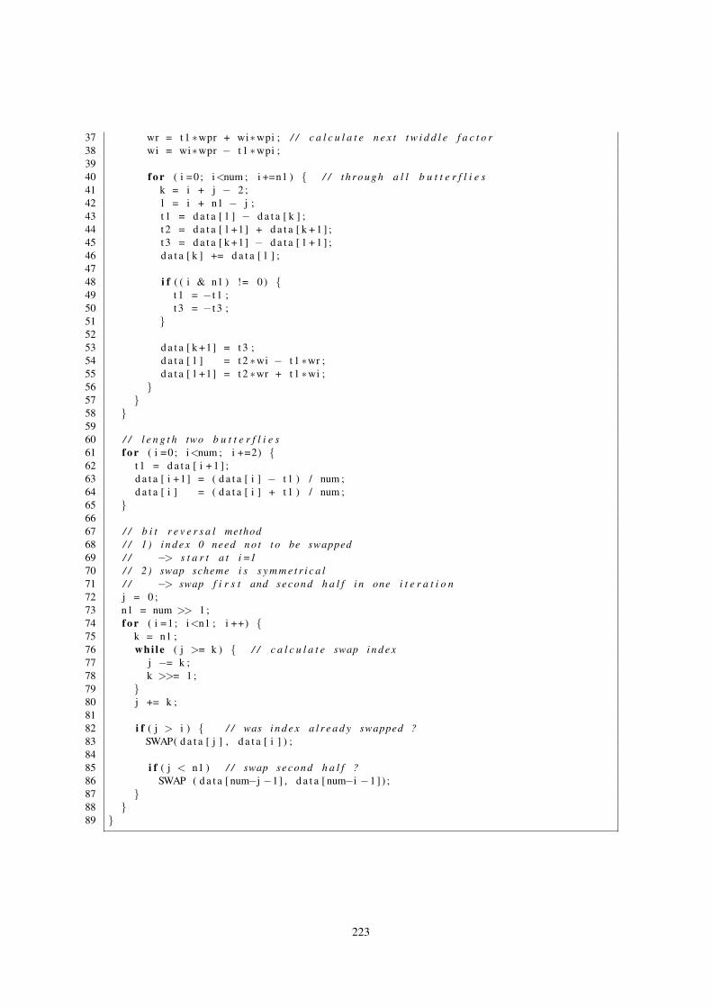
37 wr = t 1 ∗wpr + wi∗wpi ; / / c a l c u l a t e n e x t t w i d d l e f a c t o r38 wi = wi∗wpr − t 1 ∗wpi ;3940 f o r ( i =0 ; i<num ; i +=n1 ) / / t h r o u g h a l l b u t t e r f l i e s41 k = i + j − 2 ;42 l = i + n1 − j ;43 t 1 = d a t a [ l ] − d a t a [ k ] ;44 t 2 = d a t a [ l +1] + d a t a [ k + 1 ] ;45 t 3 = d a t a [ k +1] − d a t a [ l + 1 ] ;46 d a t a [ k ] += d a t a [ l ] ;4748 i f ( ( i & n1 ) != 0 ) 49 t 1 = −t 1 ;50 t 3 = −t 3 ;51 5253 d a t a [ k +1] = t 3 ;54 d a t a [ l ] = t 2 ∗wi − t 1 ∗wr ;55 d a t a [ l +1] = t 2 ∗wr + t 1 ∗wi ;56 57 58 5960 / / l e n g t h two b u t t e r f l i e s61 f o r ( i =0 ; i<num ; i +=2) 62 t 1 = d a t a [ i + 1 ] ;63 d a t a [ i +1] = ( d a t a [ i ] − t 1 ) / num ;64 d a t a [ i ] = ( d a t a [ i ] + t 1 ) / num ;65 6667 / / b i t r e v e r s a l method68 / / 1 ) i n d e x 0 need n o t t o be swapped69 / / −> s t a r t a t i =170 / / 2 ) swap scheme i s s y m m e t r i c a l71 / / −> swap f i r s t and second h a l f i n one i t e r a t i o n72 j = 0 ;73 n1 = num >> 1 ;74 f o r ( i =1 ; i<n1 ; i ++) 75 k = n1 ;76 whi le ( j >= k ) / / c a l c u l a t e swap i n d e x77 j −= k ;78 k >>= 1 ;79 80 j += k ;8182 i f ( j > i ) / / was i n d e x a l r e a d y swapped ?83 SWAP( d a t a [ j ] , d a t a [ i ] ) ;8485 i f ( j < n1 ) / / swap second h a l f ?86 SWAP ( d a t a [ num−j −1] , d a t a [ num−i −1 ] ) ;87 88 89
223
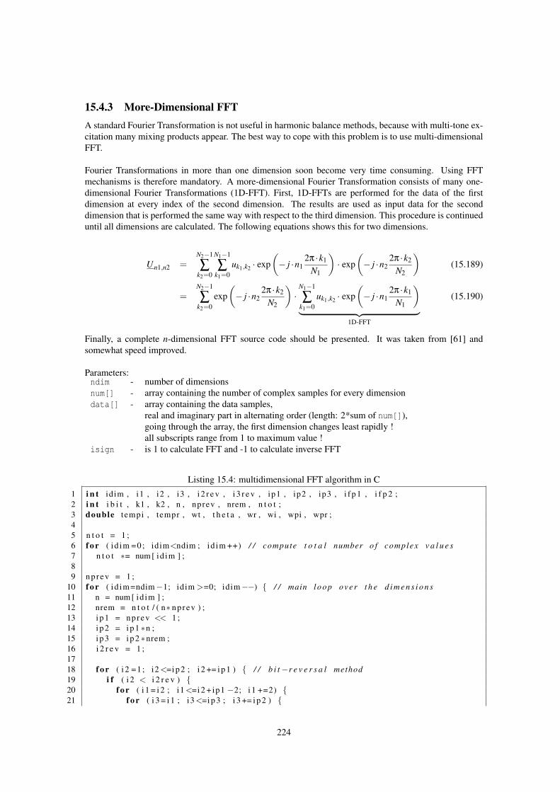
15.4.3 More-Dimensional FFTA standard Fourier Transformation is not useful in harmonic balance methods, because with multi-tone ex-citation many mixing products appear. The best way to cope with this problem is to use multi-dimensionalFFT.
Fourier Transformations in more than one dimension soon become very time consuming. Using FFTmechanisms is therefore mandatory. A more-dimensional Fourier Transformation consists of many one-dimensional Fourier Transformations (1D-FFT). First, 1D-FFTs are performed for the data of the firstdimension at every index of the second dimension. The results are used as input data for the seconddimension that is performed the same way with respect to the third dimension. This procedure is continueduntil all dimensions are calculated. The following equations shows this for two dimensions.
Un1,n2 =N2−1
∑k2=0
N1−1
∑k1=0
uk1,k2 · exp(− j ·n1
2π ·k1
N1
)· exp
(− j ·n2
2π ·k2
N2
)(15.189)
=N2−1
∑k2=0
exp(− j ·n2
2π ·k2
N2
)·
N1−1
∑k1=0
uk1,k2 · exp(− j ·n1
2π ·k1
N1
)︸ ︷︷ ︸
1D-FFT
(15.190)
Finally, a complete n-dimensional FFT source code should be presented. It was taken from [61] andsomewhat speed improved.
Parameters:ndim - number of dimensionsnum[] - array containing the number of complex samples for every dimensiondata[] - array containing the data samples,
real and imaginary part in alternating order (length: 2*sum of num[]),going through the array, the first dimension changes least rapidly !all subscripts range from 1 to maximum value !
isign - is 1 to calculate FFT and -1 to calculate inverse FFT
Listing 15.4: multidimensional FFT algorithm in C
1 i n t idim , i1 , i2 , i3 , i 2 r e v , i 3 r e v , ip1 , ip2 , ip3 , i f p 1 , i f p 2 ;2 i n t i b i t , k1 , k2 , n , nprev , nrem , n t o t ;3 double tempi , tempr , wt , t h e t a , wr , wi , wpi , wpr ;45 n t o t = 1 ;6 f o r ( id im =0; idim<ndim ; id im ++) / / compute t o t a l number o f complex v a l u e s7 n t o t ∗= num [ id im ] ;89 nprev = 1 ;
10 f o r ( id im =ndim−1; idim >=0; idim−−) / / main loop over t h e d i m e n s i o n s11 n = num [ id im ] ;12 nrem = n t o t / ( n∗ nprev ) ;13 i p 1 = nprev << 1 ;14 i p 2 = i p 1 ∗n ;15 i p 3 = i p 2 ∗nrem ;16 i 2 r e v = 1 ;1718 f o r ( i 2 =1; i2 <=i p 2 ; i 2 += i p 1 ) / / b i t−r e v e r s a l method19 i f ( i 2 < i 2 r e v ) 20 f o r ( i 1 = i 2 ; i1 <=i 2 + ip1 −2; i 1 +=2) 21 f o r ( i 3 = i 1 ; i3 <=i p 3 ; i 3 += i p 2 )
224
22 i 3 r e v = i 2 r e v + i3−i 2 ;23 SWAP( d a t a [ i3 −1] , d a t a [ i 3 r e v −1 ] ) ;24 SWAP( d a t a [ i 3 ] , d a t a [ i 3 r e v ] ) ;25 26 27 28 i b i t = i p 2 >> 1 ;29 whi le ( i b i t >= i p 1 && i 2 r e v > i b i t ) 30 i 2 r e v −= i b i t ;31 i b i t >>= 1 ;32 33 i 2 r e v += i b i t ;34 3536 i f p 1 = i p 1 ;37 whi le ( i f p 1 < i p 2 ) / / Dan ie l son−Lanzcos a l g o r i t h m38 i f p 2 = i f p 1 << 1 ;39 t h e t a = i s i g n ∗2∗ p i / ( i f p 2 / i p 1 ) ;40 wpr = cos ( t h e t a ) ;41 wpi = s i n ( t h e t a ) ;42 wr = 1 . 0 ; wi = 0 . 0 ;43 f o r ( i 3 =1; i3 <=i f p 1 ; i 3 += i p 1 ) 44 f o r ( i 1 = i 3 ; i1 <=i 3 + ip1 −2; i 1 +=2) 45 f o r ( i 2 = i 1 ; i2 <=i p 3 ; i 2 += i f p 2 ) 46 k1 = i 2 ;47 k2 = k1+ i f p 1 ;48 tempr = wr∗ d a t a [ k2−1] − wi∗ d a t a [ k2 ] ;49 tempi = wr∗ d a t a [ k2 ] + wi∗ d a t a [ k2−1];50 d a t a [ k2−1] = d a t a [ k1−1] − t empr ;51 d a t a [ k2 ] = d a t a [ k1 ] − t empi ;52 d a t a [ k1−1] += tempr ; d a t a [ k1 ] += tempi ;53 54 55 wt = wr ;56 wr = wt∗wpr − wi∗wpi ;57 wi = wi∗wpr + wt∗wpi ;58 59 i f p 1 = i f p 2 ;60 61 nprev ∗= n ;62
225

Appendix A
Qucs file formats
Qucs uses plain-text (ASCII) files as its input and transfer format for netlists and data. This appendixexplains the file formats by describing the grammars of the languages used. The files are generally line-oriented but arbitrary whitespace between the token is allowed. You can also use the backslash (\) tocontinue a line on the next line. This works almost everywhere but in comment lines.
The grammars are presented using a version of the Extended Backus-Naur Form (EBNF) which works asfollows:
A→ B Nonterminal A produces sentential form B.B|C Produces B or C.A Arbitrary repetition of form A. No repetition is allowed as well (“Kleene operator”).[ A ] Form A is optional.(A) Grouping, stands for A itself.
Nonterminal symbols are set in normal font, terminal symbols are in bold font. Terminal symbols in singlequotes are literally found in the input while the other terminal symbols are compositions. See below fordefinition of composed terminal symbols.
226

A.1 Qucs netlist grammar
Syntactic Structure
Input → InputLine InputLine → DefinitionLine
| SubcircuitBody| EquationLine| ActionLine| [ ‘#’ ( Entire line is comment ) ] Eol
A netlist is read in a line-based fashion. There are several types of lines.
Definition
DefinitionLine → Identifier ‘:’ Identifier Identifier PairList Eol
Components of the circuit are defined by providing its nodes and parameters for a property.
Subcircuits
SubcircuitBody → DefBegin DefBodyLine DefEndDefBegin → ‘.’ ‘Def’ ‘:’ Identifier Identifier EolDefBodyLine → DefinitionLine
| SubcircuitBody| Eol
DefEnd → ‘.’ ‘Def’ ‘:’ ‘End’ Eol
Subcircuits are recursively defined by blocks of component definitions.
Action
ActionLine → ‘.’ Identifier ‘:’ Identifier PairList Eol
Defines what to simulate with the circuit.
Equation
EquationLine → ‘Eqn’ ‘:’ Identifier Equation Equation EolEquation → Identifier ‘=’ ‘“’ Expression ‘“’
Named equation definitions consist of a list of assignments with expressions on their right hand side.
Declarations
PairList → Identifier ‘=’ Value Value → PropertyValue
227

| ‘“’ PropertyValue ‘“’PropertyValue → Identifier
| PropertyReal| ‘[’ PropertyReal [ ‘;’ PropertyReal ] ‘]’
PropertyReal → Real [ Scale [ Unit ] ]
The above constructs are used to define properties (parameters) of components and actions.
Mathematical Expressions
Expression → Constant| Reference| Application| ‘(’ Expression ‘)’
Constant → Real| Imag| Character| String| Range
Range → [ Real ] ‘:’ [ Real ]Reference → IdentifierApplication → Identifier ‘(’ Expression [ ‘,’ Expression ] ‘)’
| Reference ‘[’ Expression [ ‘,’ Expression ] ‘]’| ( ‘+’ | ‘-’ ) Expression| Expression ( ‘+’ |‘-’ |‘*’ |‘/’ |‘%’ |‘ˆ’ ) Expression
Operator precedence works as expected in common mathematical expressions.
Lexical structure
Identifier → Alpha AlphaNum ‘.’ Alpha AlphaNum Alpha → ‘a’ | . . . | ‘z’ | ‘A’ | . . . | ‘Z’|‘ ’AlphaNum → ‘a’ | . . . | ‘z’ | ‘A’ | . . . | ‘Z’| ‘0’ . . . ‘9’ | ‘ ’Real → [ ‘+’ | ‘-’ ] [ Num ] ‘.’ Num [ ( ‘e’ |‘E’ ) [ ‘+’ | ‘-’ ] Num ]Num → Digit Digit Digit → ‘0’ . . . ‘9’Imag → [ ‘+’ | ‘-’ ] ( ‘i’ |‘j’ ) [ Num ] ‘.’ Num [ ( ‘e’ |‘E’ ) [ ‘+’ | ‘-’ ] Num ]Character → ‘’’ ( Any character but newline and ‘’’ ) ‘’’String → ‘’’ ( Any character but newline and ‘’’ ) ‘’’Scale → ( ‘dBm’ | ‘dB’ | ‘T’ | ‘G’ | ‘M’ |‘k’ | ‘m’ | ‘u’ | ‘n’ | ‘p’ |‘f’ | ‘a’ )Unit → ( ‘Ohm’ | ‘S’ | ‘s’ | ‘K’ | ‘H’ | ‘F’ | ‘Hz’ | ‘V’ | ‘A’ | ‘W’ | ‘m’ )Eol → [ ‘\r’ ] ‘\n’
This defines the composed terminal symbols.
228

A.2 Qucs dataset grammar
Syntactic structure
Input → VersionLine Variable VersionLine → ‘<Qucs Dataset ’ Num ‘.’ Num ‘.’ Num ‘>’ Eol
The file consists of a header line indicating the software version and a number of variables.
Data
Variable → ‘<dep’ Identifier Identifier ‘>’ Float ‘</dep>’| ‘<indep’ Identifier Integer ‘>’ Float ‘</indep>’| ‘#’ ( Entire line is comment ) Eol
The Float values itself may be scattered over several lines. An independent variable denotes a list of real orcomplex values. The dependent variables denote lists of real or complex values depending on independentvariables, i.e. a function of some other variable, a f (x, . . .) in mathematical terms.
Lexical structure
Float → Real| Imag| Complex
Real → [ ‘+’ | ‘-’ ] [ Num ] ‘.’ Num [ ( ‘e’ | ‘E’ ) [ ‘+’ | ‘-’ ] Num ]Imag → [ ‘+’ | ‘-’ ] ( ‘i’ | ‘j’ ) [ Num ] ‘.’ Num [ ( ‘e’ | ‘E’ ) [ ‘+’ | ‘-’ ] Num ]Complex → Real ImagNum → Digit Digit Digit → ‘0’ . . . ‘9’Integer → [ ‘+’ | ‘-’ ] NumEol → [ ‘\r’ ] ‘\n’
229
Appendix B
Bibliography
[1] K. Kurokawa, “Power Waves and the Scattering Matrix,” IEEE Transactions on Microwave Theoryand Techniques, pp. 194–202, Mar. 1965.
[2] R. C. Compton and D. B. Rutledge, “Perspectives in Microwave Circuit Analysis,” in Proceedingsof the 32nd Midwest Symposium on Circuits and Systems, vol. 2. IEEE, Aug. 1989, pp. 716–718.
[3] M. L. Edwards and J. H. Sinsky, “A New Criterion for Linear 2-Port Stability Using a Single Ge-ometrically Derived Parameter,” IEEE Transactions on Microwave Theory and Techniques, vol. 40,no. 12, pp. 2303–2311, Dec. 1992.
[4] H.-J. Michel, Zweitoranalyse mit Leitungswellen. Teubner, 1981.
[5] S. W. Wedge and D. B. Rutledge, “Wave Techniques for Noise Modeling and Measurement,” IEEETransactions on Microwave Theory and Techniques, vol. 40, no. 11, pp. 2004–2012, Nov. 1992.
[6] A. Blum, Skriptum zur Vorlesung Elektronik IV uber Schaltungssimulation. Universitat des Saar-landes: Universitas Saraviensis, 2001.
[7] C. W. Gear, “Simultaneous Numerical Solution of Differential-Algebraic Equations,” IEEE Trans-actions on Circuit Theory, vol. 18, no. 1, pp. 89–95, Jan. 1971.
[8] S. Maas, Nonlinear Microwave and RF Circuits, second edition ed. www.artechhouse.com, 2003.
[9] D. L. Jaijeet Roychowdhury and P. Feldmann, “Cyclostationary Noise Analysis of Large RF Circuitswith Multitone Excitations,” IEEE Journal of Solid-State Circuits, pp. 324–336, Mar. 1998.
[10] V. Rizzoli and A. Neri, “State of the Art and Present Trends in Nonlinear Microwave CAD Tech-niques,” IEEE Transactions on Microwave Theory and Techniques, pp. 343–365, Feb. 1988.
[11] T. Edwards, Foundations for Microstrip Circuit Design, 2nd ed. John Wiley & Sons, 1991.
[12] T. O. Grosch and L. A. Carpenter, “Two-Port to Three-Port Noise-Wave Transformation for CADApplications,” IEEE Transactions on Microwave Theory and Techniques, vol. 41, no. 9, pp. 1543–1548, Sept. 1993.
[13] H. Shichman and D. A. Hodges, “Modeling and Simulation of Insulated-Gate Field-Effect TransistorSwitching Circuits,” IEEE Journal of Solid-State Circuits, vol. 3, no. 3, pp. 285–289, Sept. 1968.
[14] P. B. Weil and L. P. McNamee, “Simulation of Excess Phase in Bipolar Transistors,” IEEE Transac-tions on Circuits and Systems, vol. 25, no. 2, pp. 114–116, Feb. 1978.
[15] J. E. Meyer, “MOS Models and Circuit Simulation,” RCA Review, vol. 32, pp. 42–63, Mar. 1971.
[16] H. A. Wheeler, “Transmission-Line Properties of Parallel Strips Separated by a Dielectric Sheet,”IEEE Transactions on Microwave Theory and Techniques, vol. 13, no. 2, pp. 172–185, Mar. 1965.
230
[17] M. V. Schneider, “Microstrip Lines for Microwave Integrated Circuits,” The Bell System TechnicalJournal, vol. 48, pp. 1421–1444, May 1969.
[18] E. Hammerstad and Ø. Jensen, “Accurate Models for Microstrip Computer-Aided Design,” Sympo-sium on Microwave Theory and Techniques, pp. 407–409, June 1980.
[19] H. A. Wheeler, “Transmission-Line Properties of a Strip on a Dielectric Sheet on a Plane,” IEEETransactions on Microwave Theory and Techniques, vol. 25, no. 8, pp. 631–647, Aug. 1977.
[20] M. Kirschning and R. H. Jansen, “Accurate Model for Effective Dielectric Constant of Microstripwith Validity up to Millimeter-Wave Frequencies,” Electronics Letters, vol. 8, no. 6, pp. 272–273,Mar. 1982.
[21] R. H. Jansen and M. Kirschning, “Arguments and an accurate Model for the Power-Current For-mulation of Microstrip Characteristic Impedance,” Archiv fur Elektronik und Ubertragungstechnik(AEU), vol. 37, pp. 108–112, 1983.
[22] E. Yamashita, K. Atsuki, and T. Ueda, “An Approximate Dispersion Formula of Microstrip Linesfor Computer Aided Design of Microwave Integrated Circuits,” IEEE Transactions on MicrowaveTheory and Techniques, vol. 27, pp. 1036–1038, Dec. 1979.
[23] M. Kobayashi, “A Dispersion Formula Satisfying Recent Requirements in Microstrip CAD,” IEEETransactions on Microwave Theory and Techniques, vol. 36, no. 8, pp. 1246–1250, Aug. 1988.
[24] W. J. Getsinger, “Microstrip Dispersion Model,” IEEE Transactions on Microwave Theory and Tech-niques, vol. 21, no. 1, pp. 34–39, Jan. 1973.
[25] ——, “Microstrip Characteristic Impedance,” IEEE Transactions on Microwave Theory and Tech-niques, vol. 27, no. 5, p. 293, Apr. 1979.
[26] ——, “Measurement and Modeling of the Apparent Characteristic Impedance of Microstrip,” IEEETransactions on Microwave Theory and Techniques, vol. 31, no. 8, pp. 624–632, Aug. 1983.
[27] T. C. Edwards and R. P. Owens, “2-18-GHz Dispersion Measurements on 10-100-Ω MicrostripLines on Sapphire,” IEEE Transactions on Microwave Theory and Techniques, vol. 24, no. 8, pp.506–513, Aug. 1976.
[28] P. Pramanick and P. Bhartia, “An Accurate Description of Dispersion in Microstrip,” MicrowaveJournal, pp. 89–96, Dec. 1983.
[29] M. V. Schneider, “Microstrip Dispersion,” in Proceedings of the IEEE, Letters, vol. 60, Jan. 1972,pp. 144–146.
[30] M. Kirschning, R. H. Jansen, and N. H. L. Koster, “Measurement and Computer-Aided Modelingof Microstrip Discontinuities by an Improved Resonator Method,” IEEE MTT-S International Mi-crowave Symposium Digest, pp. 495–497, May 1983.
[31] M. Kirschning and R. H. Jansen, “Accurate Wide-Range Design Equations for the Frequency-Dependent Characteristic of Parallel Coupled Microstrip Lines,” IEEE Transactions on MicrowaveTheory and Techniques, vol. 32, no. 1, pp. 83–90, Jan. 1984.
[32] ——, “Corrections to ”Accurate Wide-Range Design Equations for the Frequency-Dependent Char-acteristic of Parallel Coupled Microstrip Lines”,” IEEE Transactions on Microwave Theory andTechniques, vol. 33, no. 3, p. 288, Mar. 1985.
[33] W. J. Getsinger, “Dispersion of Parallel-Coupled Microstrip,” IEEE Transactions on MicrowaveTheory and Techniques, pp. 144–145, Mar. 1973, Short Papers.
231
[34] R. H. Jansen, “High-Speed Computation of Single and Coupled Microstrip Parameters IncludingDispersion, High-Order Modes, Loss and Finite Strip,” IEEE Transactions on Microwave Theoryand Techniques, vol. 26, no. 2, pp. 75–82, Feb. 1978.
[35] M. Kirschning, R. H. Jansen, and N. H. L. Koster, “Accurate Model for open end effect of microstriplines,” Electronics Letters, vol. 17, no. 3, pp. 123–125, Feb. 1981.
[36] E. Hammerstad, “Computer-Aided Design of Microstrip Couplers with Accurate DiscontinuityModels,” Symposium on Microwave Theory and Techniques, pp. 54–56, June 1981.
[37] M. Kirschning, Entwicklung von Naherungsmodellen fur den rechnergestutzten Entwurf von hy-briden und monolithischen Schaltungen in Mikrostreifenleitungstechnik. Dissertation, UniversitatDuisburg, 1984.
[38] K. C. Gupta, R. Garg, and I. J. Bahl, Microstrip Lines and Slotlines. Artech House, Inc., 1979.
[39] K. C. Gupta, R. Garg, I. J. Bahl, and P. Bhartia, Microstrip Lines and Slotlines, 2nd ed. ArtechHouse, Inc., 1996.
[40] R. Garg and I. J. Bahl, “Microstrip discontinuities,” International Journal of Electronics, vol. 45,no. 1, pp. 81–87, 1978.
[41] R. J. Akello, B. Easter, and I. M. Stephenson, “Equivalent circuit of the asymmetric crossover junc-tion,” Electronics Letters, vol. 13, no. 4, pp. 117–118, Feb. 1977.
[42] P. Silvester and P. Benedek, “Microstrip Discontinuity Capacitances for Right-Angle Bends, T Junc-tions, and Crossings,” IEEE Transactions on Microwave Theory and Techniques, vol. 21, no. 5, pp.341–346, May 1973.
[43] A. Gopinath, A. F. Thomson, and I. M. Stephenson, “Equivalent Circuit Parameters of MicrostripStep Change in Width and Cross Junctions,” IEEE Transactions on Microwave Theory and Tech-niques, pp. 142–144, Mar. 1976, Short Papers.
[44] B. Easter, “The Equivalent Circuit of Some Microstrip Discontinuities,” IEEE Transactions on Mi-crowave Theory and Techniques, vol. 23, no. 8, pp. 655–660, Aug. 1975.
[45] M. E. Goldfarb and R. A. Pucel, “Modeling Via Hole Grounds in Microstrip,” IEEE Microwave andGuided Wave Letters, vol. 1, no. 6, pp. 135–137, June 1991.
[46] I. Bahl and P. Barthia, Microwave Solid State Circuit Design, 2nd ed. Wiley Interscience, 2003.
[47] Wikibook. (2006, Nov.) Electronics/Inductors. [Online]. Available: http://en.wikibooks.org/w/index.php?title=Electronics/Inductors
[48] R. E. Collin, Foundations for Microwave Engineering, 2nd ed. New York: Mc Graw-Hill, 1992.
[49] M. Lavrentiev and B. Chabat, Methodes de la theorie des fonctions d’une variable complexe,Moscow, 1972.
[50] M. Y. Frankel, S. Gupta, J. A. Valdmanis, and G. A. Mourou, “Terahertz Attenuation and Disper-sion Characteristics of Coplanar Transmission Lines,” IEEE Transactions on Microwave Theory andTechniques, vol. 39, no. 6, pp. 910–916, June 1991.
[51] S. Gevorgian, T. Martinsson, A. Deleniv, E. Kollberg, and I. Vendik, “Simple and accurate dis-persion expression for the effective dielectric constant of coplanar waveguides,” in Proceedings ofMicrowaves, Antennas and Propagation, vol. 144, no. 2. IEE, Apr. 1997, pp. 145–148.
[52] G. H. Owyang and T. T. Wu, “The Approximate Parameters of Slot Lines and Their Complement,”IRE Transactions on Antennas and Propagation, pp. 49–55, Jan. 1958.
232
[53] G. Ghione, “A CAD-Oriented Analytical Model for the Losses of General Asymmetric CoplanarLines in Hybrid and Monolithic MICs,” IEEE Transactions on Microwave Theory and Techniques,vol. 41, no. 9, pp. 1499–1510, Sept. 1993.
[54] K. Beilenhoff, H. Klingbeil, W. Heinrich, and H. L. Hartnagel, “Open and Short Circuits in CoplanarMMIC’s,” IEEE Transactions on Microwave Theory and Techniques, vol. 41, no. 9, pp. 1534–1537,Sept. 1993.
[55] W. J. Getsinger, “End-Effects in Quasi-TEM Transmission Lines,” IEEE Transactions on MicrowaveTheory and Techniques, vol. 41, no. 4, pp. 666–671, Apr. 1993.
[56] ——, “Circuit Duals on Planar Transmission Media,” IEEE MTT-S International Microwave Sym-posium Digest, pp. 154–156, 1983.
[57] C. Sinclair and S. J. Nightgale, “An Equivalent Circuit Model for the Coplanar Waveguide StepDiscontinuity,” IEEE MTT-S International Microwave Symposium Digest, pp. 1461–1464, Sept.1992.
[58] P. Lefferson, “Twisted Magnet Wire Transmission Line,” IEEE Transactions on Parts, Hybrids, andPackaging, vol. PHP-7, no. 4, pp. 148–154, Dec. 1971.
[59] J. A. Dobrowolski, Introduction to Computer Methods for Microwave Circuit Analysis and Design.Warsaw University of Technology: Artech House, 1991.
[60] W. Weißgerber, Elektrotechnik fur Ingenieure, Ausgleichsvorgange, Fourieranalyse, Vierpoltheo-rie ed. Vieweg Verlag, 1999, vol. 3.
[61] W. H. Press, S. A. Teukolsky, and W. T. Vetterling, Numerical Recipes in C: The Art of ScientificComputing. Cambridge University Press, 1988-1992.
[62] A. I. Zverev, Handbook of Filter Synthesis. New York: John Wiley & Sons, 1967.
[63] L. Thede, Analog and Digital Filter Design using C. New Jersey: Prentice Hall, 1996.
[64] A. S. Sedra and P. O. Brackett, Filter Theory and Design: Active and Passive, ser. Matrix Series inCircuits and Systems, A. P. Sage, Ed. Portland, Oregon: Matrix Publishers, Inc., 1978.
[65] R. K. Hoffmann, Integrierte Mikrowellenschaltungen, Elektrische Grundlagen, Dimensionierung,technische Ausfuhrung, Technologien ed. Berlin Heidelberg: Springer Verlag, 1983.
[66] B. C. Wadell, Transmission Line Design Handbook. Boston London: Artech House, Inc., 1991.
[67] M. Abramowitz and I. A. Segun, Handbook of Mathematical Functions with Formulas, Graphs, andMathematical Tables. New York: Dover Publications, Inc., May 1968.
[68] H. Stocker, Taschenbuch mathematischer Formeln und moderner Verfahren, 3rd ed. Frankfurt amMain: Verlag Harri Deutsch, 1995.
[69] J. A. Mackenzie, The Numerical Solution of Ordinary Differential Equations. University of Strath-clyde: Department of Mathematics, 2001.
[70] A. Sangiovanni-Vincentelli and A. Nardi, Computer-Aided Verification of Electronic Circuits andSystems. University of Berkeley: Department of Electrical Engineering and Computer Sciences,2002.
[71] R. Barrett, M. Berry, T. Chan, J. Demmel, J. Donato, J. Dongarra, V. Eijkhout, R. Pozo, C. Romine,and H. V. der Vorst, Templates for the Solution of Linear Systems: Building Blocks for IterativeMethods. Philadelphia, PA: SIAM, 1994.
[72] J. Berkner, Kompaktmodelle fur Bipolartransistoren, Praxis der Modellierung, Messung und Param-eterbestimmung - SGP, VBIC, HICUM und MEXTRAM ed. expert Verlag, 2002.
233
[73] E. E. E. Hoefer and H. Nielinger, SPICE - Analyseprogramm fur elektronische Schaltungen. BerlinHeidelberg: Springer Verlag, 1985.
[74] S. M. Sze, Semiconductor Devices, Physics and Technology ed. New York: John Wiley & Sons,1985.
[75] G. Engeln-Mullges and F. Uhlig, Numerical Algorithms with C. Berlin: Springer Verlag, Feb. 1996.
[76] G. H. Golub and C. F. van Loan, Matrix Computations, 3rd ed. London: The Johns HopkinsUniversity Press, 1996.
[77] G. Massobrio and P. Antognetti, Semiconductor Device Modeling with SPICE, 2nd ed. New York:Mc Graw-Hill, 1993.
[78] J. F. Hart and et al., Computer Approximations, ser. The SIAM Series in Applied Mathematics. NewYork: John Wiley & Sons, Inc., 1968.
[79] National Institute of Standards and Technology. (2003, Dec.) Fundamental Physical Constants fromNIST. [Online]. Available: http://physics.nist.gov/cuu/Constants/index.html
[80] A. C. M. de Queiroz, “Compact Nodal Analysis With Controlled Sources Modeled by OperationalAmplifiers,” in Proceedings of the 38th Midwest Symposium on Circuits and Systems, vol. 2. IEEE,Aug. 1995, pp. 1205–1208.
[81] L. M. Wedepohl and L. Jackson, “Modified nodal analysis: an essential addition to electrical circuittheory and analysis,” Engineering Science and Education Journal, vol. 11, pp. 84–92, June 1992.
[82] V. A. Monaco and P. Tiberio, “Computer-Aided Analysis of Microwave Circuits,” IEEE Transac-tions on Microwave Theory and Techniques, vol. 22, no. 3, pp. 249–263, Mar. 1974.
[83] E. Yamashita, K. Atsuki, and T. Hirahata, “Microstrip Dispersion in a Wide-Frequency Range,”IEEE Transactions on Microwave Theory and Techniques, vol. 29, no. 6, pp. 610–611, June 1981.
[84] M. Kirschning, R. H. Jansen, and N. H. L. Koster, “Measurement and Computer-Aided Modeling ofMicrostrip Discontinuities by an Improved Resonator Method,” Symposium on Microwave Theoryand Techniques, pp. 495–497, May 1983.
[85] M. Kobayashi, “Important Role of Inflection Frequency in the Dispersive Property of MicrostripLines,” IEEE Transactions on Microwave Theory and Techniques, vol. 30, no. 11, pp. 2057–2059,Nov. 1982.
[86] P. Bhartia and P. Pramanick, “A New Microstrip Dispersion Model,” IEEE Transactions on Mi-crowave Theory and Techniques, vol. 32, no. 10, pp. 1379–1384, Oct. 1984.
[87] M. Kobayashi, “Frequency Dependent Characteristics of Microstrips on Anisotropic Substrates,”IEEE Transactions on Microwave Theory and Techniques, vol. 30, no. 11, pp. 2054–2057, Nov.1982.
[88] H. A. Atwater, “Tests of Microstrip Dispersion Formulas,” IEEE Transactions on Microwave Theoryand Techniques, vol. 36, no. 3, pp. 619–621, Mar. 1988.
[89] E. J. Denlinger, “Losses of Microstrip Lines,” IEEE Transactions on Microwave Theory and Tech-niques, vol. 28, no. 6, pp. 513–522, June 1980.
[90] H. A. Wheeler, “Transmission-Line Properties of Parallel Wide Strips by a Conformal-MappingApproximation,” IEEE Transactions on Microwave Theory and Techniques, vol. 12, no. 3, pp. 280–289, May 1964.
[91] R. P. Owens, J. E. Aitken, and T. C. Edwards, “Quasi-Static Characteristics of Microstrip on anAnisotropic Sapphire Substrate,” IEEE Transactions on Microwave Theory and Techniques, vol. 24,no. 8, pp. 499–505, Aug. 1976.
234
[92] M. Kirschning, R. H. Jansen, and N. H. L. Koster, “Coupled Mircrostrip Parallel-Gap Model forImproved Filter and Coupler Design,” Electronics Letters, vol. 19, no. 10, pp. 377–379, May 1983.
[93] G. Ghione and C. U. Naldi, “Coplanar Waveguides for MMIC Applications: Effect of Upper Shield-ing, Conductor Backing, Finite-Extent Ground Planes, and Line-to-Line Coupling,” IEEE Transac-tions on Microwave Theory and Techniques, vol. 35, no. 3, pp. 260–267, Mar. 1987.
[94] ——, “Analytical Formulas for Coplanar Lines and Monolithic MICs,” Electronics Letters, vol. 20,no. 4, pp. 179–181, Feb. 1984.
[95] S. S. Bedair and I. Wolff, “Fast, Accurate and Simple Approximate Analytic Formulas for Cal-culating the Parameters of Supported Coplanar Waveguides for (M)MIC’s,” IEEE Transactions onMicrowave Theory and Techniques, vol. 40, no. 1, pp. 41–48, Jan. 1992.
[96] J. L. B. Walker, “A Survey of European Activity on Coplanar Waveguide,” IEEE MTT-S Interna-tional Microwave Symposium Digest, pp. 693–696, 1993.
[97] C. Veyres and V. F. Hanna, “Extension of the application of conformal mapping techniques to copla-nar lines with finite dimensions,” International Journal of Electronics, vol. 48, no. 1, pp. 47–56,1980.
[98] P. Russer and S. Muller, “Noise Analysis of Microwave Circuits with General Topology,” Symposiumon Microwave Theory and Techniques, pp. 1481–1484, 1992.
[99] ——, “Noise Analysis of Microwave Circuits with General Topology and Arbitrary Representation,”Asia-Pacific Microwave Conference, pp. 819–822, 1992.
[100] H. Hillbrand and P. H. Russer, “An Efficient Method for Computer Aided Noise Analysis of LinearAmplifier Networks,” IEEE Transactions on Circuits and Systems, vol. 23, no. 4, pp. 235–238, Apr.1976.
[101] ——, “Correction to ”An Efficient Method for Computer Aided Noise Analysis of Linear AmplifierNetworks”,” Letters to the Editor, p. 691, July 1976.
[102] R. A. York and R. C. Compton, “Experimental Evaluation of Existing CAD Models for MicrostripDispersion,” IEEE Transactions on Microwave Theory and Techniques, vol. 38, no. 3, pp. 327–328,Sept. 1990.
[103] M. Kobayashi and N. Sawada, “Analysis and Synthesis of Tapered Microstrip Transmission Lines,”IEEE Transactions on Microwave Theory and Techniques, vol. 40, no. 8, pp. 1642–1646, Aug. 1992.
[104] H. J. Carlin, “A Simplified Circuit Model for Microstrip,” IEEE Transactions on Microwave Theoryand Techniques, pp. 589–591, Apr. 1973, Short Papers.
[105] H. J. Carlin and P. P. Civalleri, “A Coupled-Line Model for Dispersion in Parallel-Coupled Mi-crostrips,” IEEE Transactions on Microwave Theory and Techniques, pp. 444–446, May 1975.
[106] R. Garg and I. J. Bahl, “Characteristics of Coupled Microstriplines,” IEEE Transactions on Mi-crowave Theory and Techniques, vol. 27, no. 7, pp. 700–705, July 1979.
[107] H. Cory, “Dispersion Characteristics of Microstrip Lines,” IEEE Transactions on Microwave Theoryand Techniques, vol. 29, no. 1, pp. 59–61, Jan. 1981.
[108] N. G. Alexopoulos and S.-C. Wu, “Frequency-Independent Equivalent Circuit Model for MicrostripOpen-End and Gap Discontinuities,” IEEE Transactions on Microwave Theory and Techniques,vol. 42, no. 7, pp. 1268–1272, July 1994, Short Papers.
[109] P. Silvester and P. Benedek, “Equivalent Capacitances of Microstrip Open Circuits,” IEEE Transac-tions on Microwave Theory and Techniques, vol. 20, no. 8, pp. 511–516, Aug. 1972.
235

[110] W. J. R. Hoefer, “Equivalent Series Inductivity of a Narrow Transverse Slit in Microstrip,” IEEETransactions on Microwave Theory and Techniques, vol. 25, no. 10, pp. 822–824, Oct. 1977.
[111] C. Descharles, C. Algani, B. Mercier, and G. Alquie, “Physical and Electrical Modelling of BondingWires up to 110 GHz,” 33rd European Microwave Conference, vol. 2, pp. 639–624, 2003.
236