Embed Size (px)
Citation preview
AD-A115 551 AIR FORCE INST OF TECH WRIGHT-PATTERSNABO CO-EC FG1AC RESONANT CHARGING FOR INTERFACIN PRIME POWER TO PULSE CONOI-T()DEC 81 V C OUNGAN
UNCLASSIFIED AFIT/GE/EE/1O-18 NL
EnhmmEhhhEEE-mImhhmhhhhhlmm"'I'D'-'-"mon

A - -- ,~---
.7 rP9.t I
yu0
ti t!!~'f~
I
I
A a -.~
~ ~!t~
A. I -~ ~ ~ ~ ~ta~ F
,~' ~
p
~-1'
AFIT/GE/EE/81D-18
AC RESONANT CHARGING FOR INTERFACING
PRIME POWER TO PULSE CONDITIONING CIRCUITS
THESIS
AFIT/GE/EE/81D-18 William C. Dungan
Capt USAF
ApDIS rIBlmONSATc f l-A-
Urdi-nited
AFIT/GE/EE/81D-18
AC RESONANT CHARGING FOR INTERFACING
PRIME POWER TO PULSE CONDITIONING CIRCUITS
THESIS
Presented to the Faculty of the School of Engineering
of the Air Force Institute of Technology
Air University
in Partial Fulfillment of the
Requirements for the Degree of
Master of Science
by
William C. Dungan, B.S.
Captain USAF
Graduate Electrical Engineering
December 1981
Approved for public release; distribution unlimited.

AFIT/GE/EE/81D-18
Preface
This thesis project has been one of the most challenging experiences
I have encountered. I am grateful to Dr. Frederick Brockhurst for intro-
ducing me to the AC resonant charging topic and to Dr. Robert Fontana and
Capt. Tim Skvarenina for their counsel after Dr. Brockhurst's retirement
from the Air Force.
Before entering AFIT I was fortunate enough to visit the Electric
Power Laboratory at MERADCOM. I was quite impressed with the personnel,
facilities, and general work philosophy and tried to get an assignment
into the organization. Though this was not possible it did open the door
for this research project which was conducted at MERADCOM's Electrical
Equipment Division. Quite a number of people in this organization sup-
ported this thesis effort. I am grateful to them and especially to my
advisors Dr. Alois L. Jokl, Dr. Larry I. Amstutz, and Dr. James Ferrick
and also to Mr. Michael Mando. Each of these individuals played a unique
and invaluable role during the research process. Their knowledge, exper-
ience, and professionalism was tinted with enough empathy to gain for
them my deepest respect. I would also like to thank Mr. Carl Heise for
providing me with needed expertise on machine theory and Mr. Bobbie
Browning and Mr. Gerald Sullivan for their assistance during the experi-
mental tests.
I am also appreciative of the enthusiastic support given this study
by Mr. James P. O'Loughlin of the Air Force Weapons Laboratory and Dr.
Richard W. Gilchrist of Clemson University. These individuals provided
both stimulating discussion and advice on sidestepping a number of pit-
falls. Finally, a special thanks goes to my wife, Donna, for her help
and understanding during this study.
William C. Dungan
ii
Contents
Page
Preface. ....................... .. .. .. ..
List of Figures. ........................... v
List of Tables...........................vi
Abstract ............................. vii
I. Introduction .......................... 1
Background ......................... 1Problem and Scope. ..................... 2Approach .......................... 3Sequence of Presentation .................. 3
II. Theory of AC Resonant Charging ................. 5
The Pulser ......................... 5The Discharge Circuit. ................... 5The Charging Circuit .................... 7The MERADCOM Pulser .. .................... 10General Approach to Theoretical Analysis ......... 11Theoretical Analysis of the Discharge Circuit. ...... 12Theoretical Analysis of the Charging Circuit ....... 14
III. Results and Discussion. ................... 20
System Grounding and Noise. ............... 20The Discharge Circuit .. ................. 22The Charging Circuit. .................. 24
Alternator Terminal Measurements of Voltage andCurrent .. ...................... 24Pulser Measurements .. ................ 25Charging Current Anomalies. ............. 27Charging Voltage Anomaly ............... 28
Resonance Determination .. ................ 32
IV. Conclusions and Recommendations. ............... 44
Conclusions ....................... 44Recommendations .. .................... 45 4~
Bibliography. ........................... 47 Dy GFr
Appendix A: Theoretical Development of the AC Resonant Z.,Charging Equations .. ................. 48
Appendix B: Program Equate. .. .................. 57
'iTt 4;5 t.1,
~eo,
Contents
( Page
Appendix C: ........... ........................... . 60
i Operating Instructions for RKFOUR .. ........ . 61The Basic RKFOUR Program .... ............. ... 66Subroutine RKFOUR ...... ................ . 69Program RLCCHG ....... .................. .. 72Program RLCDIS ....... .................. .. 74
Appendix D: Equipment List ....... ................... .. 76
Appendix E: Leakage Transformer Short-Circuit Test . ....... . 78
Vita ............. ............................... . 79
iv
.,'
4'1
I.1

List of Figures
Figure Page
1 Typical Discharge Circuit of a Pulser ..... .......... 6
2 Simplified Discharge Circuit for the MERADCOM Pulser 6
3 Block Diagram for the Complete Pulser Circuit ... ...... 9
4 Schematic Diagram of the MERADCOM Pulser ... ........ 9
5 Pulser Discharge Current Using Program RLCDIS ...... . 12
6 Discharge Circuit Capacitive and Inductive VoltagesUsing Program RLCDIS ...... .................. .. 13
7 Simplified Circuit for Half Cycle Charging . ....... . 14
8 Charging Circuit for the AC Resonant Mode ......... ... 15
9 Charging Current for the MERADCOM Pulser Using Program
EQUATE .......... ......................... . 17
10 Charging Current, Capacitor and Inductor Voltages forthe MERADCOM Pulser Using Program EQUATE .. ........ . 18
11 Pulser Discharge Current ..... ................ . 23
12 Primary Current and Voltage at the Alternator Terminals 23
13 Charging Current and Voltage .... .............. . 26
14 Initial Rise of the Charging Current .. .......... . 26
15 Initial Charging Voltage Curve with Transient ....... .. 29
16 Blowup of Charging Voltage Curve Transient . ....... . 29
17 Simplified Pulser Schematic for Studying the Charge/
Discharge Interaction ...... .................. . 30
18 Alternator Vector Diagram Using Steady State ReactanceComponents (2275 RPM) ....... .................. .. 40
v

List of Tables
Table Page
1 Data used to Study the Alternator Response and its
Internal Reactance .. ..................... 37
vi
AFIT/GE/EE/81D-18
fAbstract
The impact on a prime power source due to AC resonant charging was
investigated. The source was a standard DOD 15 KW, 400 Hz alternator.
Adverse impact on the alternator was almost negligible for a varying load
of 15 to 60 KW and a frequency change of 380 to 475 Hz. The only excep-
tion was caused by the pulser diodes. Their turn-on was reflected in
the alternator voltage waveforms. An indirect approach is presented
for determining resonance and, thus, the internal reactance contribution
by the alternator. This value was found to be slightly less than that
specified for the leakage reactance. The investigation concludes that
resonance, in the classical steady state sense, is never reached. Even
though the charging circuit has a transient response, the alternator
armature reaction is approximately fixed. This implies that the alter-
nator is in a near steady state mode of operation.
vii
AC RESONANT CHARGING FOR INTERFACINGf PRIME POW4ER TO PULSE CONDITIONING CIRCUITS
I. Introduction
Background
The advent of directed energy weapons has spurred the development
of a large number of supporting technologies. Two of these are the
power source and power conditioning. The development of these techno-
logy areas has been driven by several factors. Primary among these are
the beam weapon's inefficiency (requirement for high power), voltage and
current waveshaping (requirement for advanced power conditioning), and
dependable interfacing of the power source with the power conditioning
equipment (requirement for lightweight, low volume charging of the inter-
mediate energy store). The last of these is the topic of concern for
this research effort.
The Army and Air Force are both concerned with the interface problem
and have expended considerable resources toward its resolution. The
* Army's need stems from the requirement for systems that are ground mobile.
Thus, all equipment in this general category must be relatively light and
itlow volume. The Air Force requirements are even more stringent since its
systems must be flyable.
One possible way to resolve the interface problem is by the use of
AC resonant charging. This method employs an AC voltage source to
recharge the energy storage condenser of a voltage-fed network. It has
been the subject of only a small number of tests. Thus, there is only
limited information (and understanding) concerning the interface between
the alternator and the charging system during its use.
In 1976 Airesearch Manufacturing Company submitted their findings
for the AC resonant charging tests they had performed on a modifiedI, alternator (Ref 9). One of the secondary objectives of the program was
to test the machine and its loading circuit at precise resonant condi-
tions. Although this objective was not met, the machine was tested at
two different off-resonant conditions. This study was sponsored by the
Air Force Weapons Laboratory (AFWL). The AFWL also sponsored the 1978
Power Generation Study and Test Program which was conducted by the Mobi-
lity Equipment Research and Development Command (MERADCOM), Ft. Belvoir,
Virginia. Among other conclusions, it found that including all of the
AC resonant charging inductance inside the alternator was not only
feasible but could also provide an overall weight saving for the system.
Most of the charging inductance is normally included in a high leakage
transformer.
The latest effort involving AC resonant charging is a program being
conducted by Clemson University and sponsored by the Aero Propulsion Lab-
oratory at Wright-Patterson AFB, Ohio. The Clemson investigators are
developing computer simulations which are designed to predict the internal
* inductance of the power source during the AC charging mode. Thus, the
results of this thesis research effort should serve as a weighted input
to either refine or validate the Clemson predictions.
Problem and Scope
The major problem was the lack of a full understanding of the inter-
action of the alternator with the remainder of the charging circuit during
the AC resonant charging mode. The impact on the alternator needed to be
determined for varying loads and frequencies. It was believed that this
mode of operation did not have the same adverse impact on the alternator
2
as did DC resonant charging (Ref 8:50). However, this needed to be
confirmed. Also, an investigation needed to be made to determine what
( actually constitutes resonance, when does it occur, and when it does
occur what is the effective internal machine reactance. To gain a
fuller understanding of the charging system, attention also had to be
given to the discharge circuit, system grounding (loops), system noise,
pulse triggering, and the physical layout of the pulser. Thus, the study
was primarily concerned with the charging system and minimal effort was
devoted to other system aspects such as the discharge circuit.
Approach
The first step in this investigation was a review of AC resonant
charging theory. The equatiors derived theuia tically were then consoli-
dated into a computer program called EQUATE that developed the data needed
to provide plots of the circuit voltages and current. Following this the
Runge-Kutta programs RLCCHG and RLCDIS were written to integrate the dif-
ferential equations of the charge and discharge circuits, respectively.
These latter programs solved the system equations for all frequencies
while program EQUATE was applicable only at the circuit resonant fre-
quency. Once these theoretical models were developed, the experimental
effort began. The system was configured and tested at 15, 30, 45, and
briefly, at 60 kilowatts. Special tests were also made in order to
determine resonance and, thus, the effective machine reactance.
Sequence of Presentation
A detailed description of AC resonant charging theory is presented
in Chapter II. Chapter III describes the experimental results and their
analyses. The project conclusions and recommendations for future study
3
are presented in the final chapter.
There are also five appendices. Appendix A presents a detailed
development of the half cycle charging equations. Appendix B provides
a listing of program EQUATE. Appendix C includes the operating instruc-
tions for developing programs which will use the subroutine RKFOUR. It
also provides a listing of RKFOUR, RLCCHG, and RLCDIS. Appendix D con-
tains a list of the test equipment. The last appendix gives the results
of the leakage transformer short-circuit test.
!4
I
II. Theory of AC Resonant Charging
While the theory of AC resonant charging has been known for at
least the last four decades it has yet to receive thorough publication
coverage. The "grandfather text" is Pulse Generators (Ref 2) which was
edited by Glasoe and Lebacqz shortly after World War II. The following
material is a brief synopsis taken from this text.
The Pulser
The circuit that delivers the pulses of energy to a load is referred
to as a "line-type pulser." This type of pulser discharges all of its
energy during each pulse. The scope of this presentation does not cover
the "hard-tube pulser" which delivers only a small fraction of its stored
energy into the load during a single pulse. Generally, the discussion of
a pulser can logically be divided into two categories, the charge and dis-
charge circuits. This is possible since the charging of the energy-storage
component of the pulser requires a time that greatly exceeds the discharge
time. The discharge circuit will be introduced. However, this presenta-
tion will be directed primarily at the charging circuit.
The Discharge Circuit
The basic discharge circuit of a pulser can be represented schemati-
cally as shown in Figure 1. If the energy for the pulse is stored in the
electrostatic field of a capacitor(s), then the unit is a "voltage-fed
network" as opposed to a "current-fed network" which stores its energy
in a magnetic field. This energy storage device is often referred to as
a "pulse-forming network" or PFN. "When the load impedance is equal to
the characteristic impedance of the network, assuming the switch to have
negligible resistance, all the energy stored in the network is transferred
5
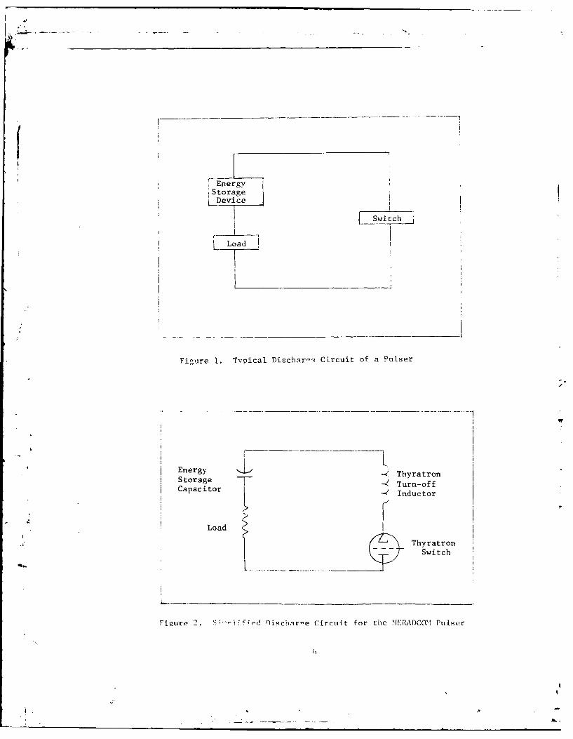
SEnergy
StorageiDevice
Switch
L Load
Figure 1. Typical Dischar-" Circuit of a Pulser
kV
Energy ThyratronStorage Capaitor 7 Turn-off
Capacitor -Inductor
Load
Thyratron
Switch
i
Figure 2. SqiI f;(od Nichar-e Circuit for the MIEP\DCOM Pulser
• 6
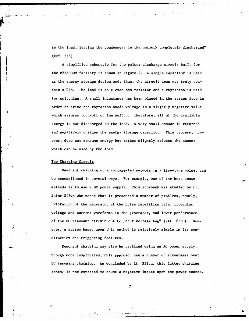
to the load, leaving the condensers in the network completely discharged"
(Ref 2:8).f A simplified schematic f or the pulser discharge circuit built for
the HERADCOM facility is shown in Figure 2. A single capacitor is used
as the energy storage device and, thus, the circuit does not truly con-
tain a PFN. The load is an eleven ohm resistor and a thyratron is used
for switching. A small inductance has been placed in the series loop in
order to drive the thyratron anode voltage to a slightly negative value
which assures turn-off of the switch. Therefore, all of the available
energy is not discharged to the load. A very small amount is returned
and negatively charges the energy storage capacitor, This process, how-
ever, does not consume energy but rather slightly reduces the amount
which can be used by the load.
The Charging Circuit
Resonant charging of a voltage-fed network in a line-type pulser can
be accomplished in several ways. For example, one of the best known
methods is to use a DC power supply. This approach was studied by Lt.
Jaime Silva who noted that it presented a number of problems, namely,
"vibration of the generator at the pulse repetition rate, irregular
voltage and current waveforms in the generator, and lower performance
* * of the DC resonant circuit due to input voltage sag" (Ref 8:50). How-
ever, a system based upon this method is relatively simple in its con-
struction and triggering features.
- Resonant charging may also be realized using an AC power supply.
Though more complicated, this approach has a number of advantages over
DC resonant charging. As concluded by Lt. Silva, this latter charging
scheuim is not expected to cause a negative impact upon the power source.
7
However, it does require that the AC source frequency be integrally( related to the pulse recurrence frequency (PRF). This is necessary
since the charging period must terminate at a current zero crossing.
As there are only two zero crossings per cycle, the PRF must not be
greater than twice the AC frequency. The relationship between the PRF
and the AC frequency is given by the following equation.
PRF -Z KfA (1)
where
K = 1,2...
f AC = impressed AC frequency
A value of K = 1 corresponds to half cycle charging and K =2 to full
cycle charging. If the PRF is twice the AC frequency then the network
voltage attains a value approximately 7T/2 times the peak AC voltage.
Though this fixed frequency requirement allows little flexibility in the
alternator-pulser interface, the deficiency is offset somewhat by the
advantage of being able to control the pulse power output by varying the
alternator field current. Another advantage is that this system permits
a net saving in weight and size relative to the DC system. its block
diagram is shown in Figure 3.
There are a number of requirements levied upon this circuit. Among
them is the need for high efficiency. This normally eliminates the use
of a resistor for the charging element since its inherent efficiency can
never exceed 50 per cent. The charging element must allow the discharge
of the network at a peak voltage. It must also be capable of isolating
the source from the time the switch closes until it deionizes (for a
gaseous switch). For example, if the network is connected directly to
8
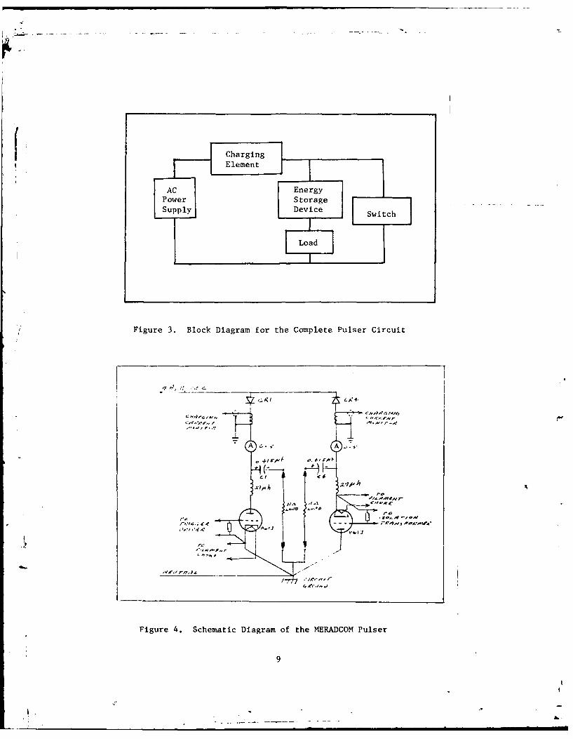
i ElementAAC Energy
Supply Device Switch
[Load I
Figure 3. Block Diagram for the Complete Pulser Circuit
4-15" (" ~A 4-SuS~
A 6 +1
.2 IP
reo
.Fi/ue4 /S D o
; Figure 4. Schematic Diagram of the MERADCOM Pulser
t , . ...2 . . .. .
the high voltage terminals of a transformer and discharged at a voltage
peak, the network begins to recharge immediately, the switch fails to
re-open, and the transformer is short-circuited for the remainder of
the half cycle.
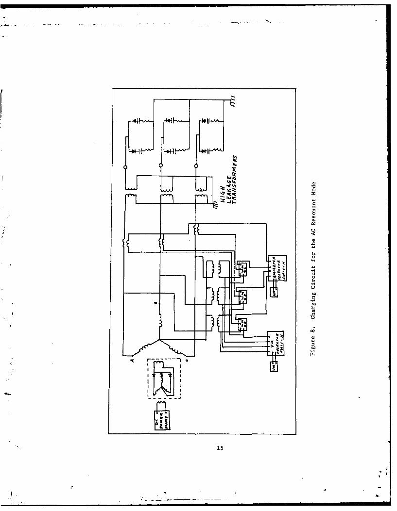
This problem may be avoided by placing a hold-off diode between the
high voltage transformer and the energy storage network. Figure 8 shows
such an arrangement. The network (capacitor) may now be discharged during
the following half cycle which has a polarity opposite to that of the
charging half cycle. This provides stable circuit action and eliminates
the problem associated with the continual build-up of the charging voltage
and current should the discharge circuit switch fail to operate (close).
As shown in Figure 8, all phases have two charging circuits and each of
these contains a hold-off diode. One circuit network is charged during
a positive half cycle and the other is charged during a negative half
cycle. The transformer utilization factor is greatly improved by this
approach.
The MERADCOM Pulser
These advantages are incorporated in the circuit of Figure 4. This
circuit is the basis for the MERADCOM pulser. It provides a more detailed
account of one of the phase networks of Figure 8. A description of its
operation will now be presented.
During the positive half cycle capacitor Cl, the energy storage
device, is charged. The voltage on Cl, VCI, reaches its peak when the
source (alternator) voltage and charging current pass through zero. VCI
remains at this peak value for a brief time into the negative half cycle.
When the source voltage reaches a specified negative value a trigger
pulse is sent to the thyratron in the Cl discharge circuit. The thyratron
10
fires and discharges the stored energy into the 11 ohm resistive load.
As the discharge current tends to zero, the voltage on the small inductor
at the switch anode reverses polarity. This forces a slight negative
charge on Cl which assures proper turn-off of the thyratron. During the
negative half cycle the source charges C4 and the same chain of events
occur as described for Cl.
General Approach to the Theoretical Analysis
Independent theoretical analyses were performed on both the discharge
circuit and the charge cirrnit of the pulser. A number of computer pro-
grams were developed. These divide into two geA i orimes as implied
in the introduction. The first of these was simply an application of the
AC resonant charging equations derived in Appendix A. These equations
were used to show how the circuit current and voltages varied over a
half cycle of charging. However, their use was applicable only to a cir-
cuit operating at the resonant frequency. This program of equations is
listed in Appendix B as Program EQUATE.
The second program category was based upon the use of a Runge-Kutta
integration subroutine called RKFOUR which was developed by B. D. Weathers.
Programs were developed, following his suggested format, that would inte-
grate the differential equations for a number of cases. The most useful
of these were Program RLCCHG and Program RLCDIS which integrated the
charge and discharge circuit equations, respectively. Program RLCDIS
was obtained by slightly modifying Program RLCCHG. Both of these programs,
as well as RKFOUR and instructions for its use, are listed in Appendix C.
They each integrate their respective circuit equations over a half cycle.
Program RLCCHG was found to be particularly useful since it, in contrast
to Program EQUATE, is capable of integrating the charging circuit equations
11
at off-resonant frequencies.
Theoretical Analysis of the Discharge Circuit
As noted earlier, the discharge circuit for the MERADCOM pulser can
be represented by the schematic shown in Figure 2. The differential
equations for this circuit were integrated using Program RLCDIS with the
resistance of the switch neglected. The current and voltage curves shown
in Figures 5 and 6 resulted from the selection of a 0.43 Uif capacitor,
an 11 ohm load resistor, and a 29 ph inductor. The capacitor was
P / 1 !A 2W
CI i $
I I --t I .
E
R
4 I IDI S
8.888 8.832 8.850 8.875 8.18 8.125 8.150 8,175
TIME Xi8-4
Figure 5. Pulser Discharge Current Using Program RLCDIS
12
ii
7500
5000
I1\0i
A88I I f
-50 -7
T - -- V
T- I 1-
Figre6. ishare irci aaiieadIdcieVlae
Usn rgrmRCI
I.' I13
initially charged to -6000 volts. This value was read from the oscillo-
grams for a load of approximately 20 KW. As seen in the curves, at the
time of the current zero crossing the capacitor voltage has reversed its
polarity. This reverse charge forces the thyratron switch to turn off.
Thus, the discharge circuit is isolated from the charging circuit through-
out the interpulse period.
Theoretical Analysis of the Charging Circuit
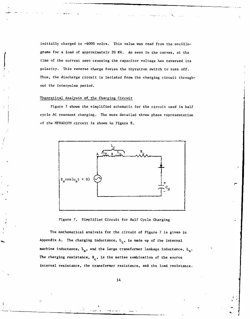
Figure 7 shows the simplified schematic for the circuit used in half
cycle AC resonant charging. The more detailed three phase representation
of the MERADCOM circuit is shown in Figure 8.
LC
E a COS at + +7 )C N
Figure 7. Simplified Circuit for Half Cycle Charging
The mathematical analysis for the circuit of Figure 7 is given in
Appendix A. The charging inductance, Lc, is made up of the internal
machine inductance, La, and the large transformer leakage inductance, Lx .
The charging resistance, Rc, is the series combination of the source
internal resistance, the transformer resistance, and the load resistance.
14
"44
I~j4U
14, c
.........
15.
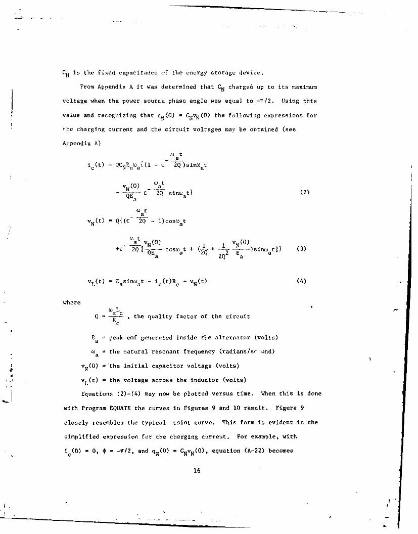
CN is the fixed capacitance of the energy storage device.
From Appendix A it was determined that CN charged up to its maximum
voltage when the power source phase angle was equal to -7/2. Using this
value and recognizing thatN = CN(0) the following expressions for
the charging current and the circuit voltages may be obtained (see
Appendix A)
toa
ic(t) = QCNEaua{(l - C 2Q)sinwat
VN (O) _a t s t- £ 2Q sineuatI (2)QEa a
(dta
vN(t) = Q{(C 2Q - l)cosca t
t~iVN(O) 1 1vN(0)+ 2Q t QE--- coscat + ( + + )sinwat]) (3)a 2Q 2 E a
vL(t) Easin at - i c (t)Rc - N(t) (4)
where
Q ac the quality factor of the circuitRc
Ea = peak emf generated inside the alternator (volts)
Wa = the natural resonant frequency (radians/sr-ond)
vN(O) = the initial capacitor voltage (volts)
vL(t) = the voltage across the inductor (volts)
Equations (2)-(4) may now be plotted versus time. When this is done
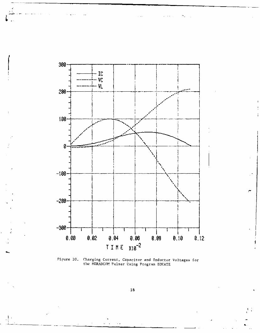
with Program EQUATE the curves in Figures 9 and 10 result. Figure 9
closely resembles the typical tsint curve. This form is evident in the
simplified expression for the charging curreut. For example, with
ic (0) 0 0, - -7r/2, and qN(O) CNvN(O), equation (A-22) becomes
16
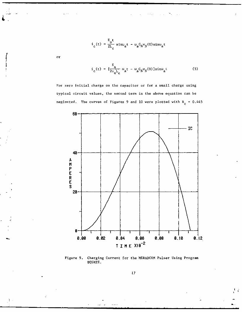
Etc t 2L sin at - aCNVN(0)sinwat
C
( orE
c 2waL W at - WaCNvN(O) lsinat (5)a c
For zero initial charge on the capacitor or for a small charge using
typical circuit values, the second term in the above equation can be
neglected. The curves of Figures 9 and 10 were plotted with Rc = 0.445
IC
MPERES
0.08 8.02 0.04 0.86 8.08 0.10 0.12
T I M E X18- 2
Figure 9. Charging Current for the MERADCOM Pulser Using ProgramEQUATE.
17
308- i "iVIC ,,
f30~J - I-1 ----- I-, ", I _ _
4- -
4-2
0- Ir8
* I
8.08 8.02 0.84 8.86 0.88 8.8 80 .12.,T I ME xto-2
Figure 10. Charging Current, Capacitor and Inductor Voltages forthe MERADCOM Pulser Using Program EQUATE
18
ohms, C N =147 lif vN (0)=-5.4 volts, E a = 150 volts, and Lc= 0.858 mh.
These values were selected early in this study. Their substitution into
( equation (5) yields
Sc (t) = (87413t + l.99)sin2802t (6)
The Results section will show that the above values are not very different
from the final values which were either measured or calculated.
With the exception of the first 22 microseconds, the complete half
charging cycle (1.12 msec) is dominated by the first term in equation (6),
that is, the w tsinw a t term. Since the charging voltage v N(t) is a func-
titon of the integral of the current it will reach its maximum value at
the end of the charging half cycle (7T radians). Again, the purpose of
the diode in Figure 7 is to block the circuit's attempt to lower this
voltage after it has reached its peak value. Without the diode the
current would go negative at the end of the half cycle. This would cause
a reverse polarity on the capacitor which, at the end of a full cycle,
would be twice the half cycle value. This is known as full cycle charging.
Without proper controls the voltage could, as explained earlier, build up
to a dangerous level, especially should the discharge switch fail to
operate. With half cycle charging this disadvantage is eliminated.
19
III. Results and Discussion
The circuit of Figure 8, with the discharge switch branch included,
was set up and testing was begun. However, the circuit was later par-
tially disconnected to confirm the resistance, inductance, and capaci-
tance values of the major components. These components are listed in
some detail in Appendix D. The per phase DC resistance of the alterna-
tor was found to be approximately 0.18 ohms. This value was multiplied
by a factor of 1.5 to account for the resistive change due to loss
mechanisms such as hysteresis and eddy currents (Ref 4:255; 5:227-237).
A short circuit test of the C phase high leakage transformer was then
conducted. The results of this test are recorded in Appendix E where
all values are referred to the low voltage side of the transformer. The
resistance and inductance (at 400 Hz) were found to be 0.1427 ohms and
0.690 mh, respectively. Also, a capacitance of 0.415 v'f was measured
for one of the energy storage (charging) capacitors. Since these tests
were not performed initially, some of the earlier theoretical analyses
(plots, for example) were based on slightly different nominal component
values.
System Grounding and Noise
During the early stages of testing the pulser system was found to
be inherently noisy. It was this problem that restricted Lt Silva's
operation of the system to a low power level. His report indicates that
multiple trigger signals prevented the build-up of voltage on the charging
capacitors and that this malfunction was caused by the electronic logic
circuit (Ref 8). He did not have sufficient time to diagnose this prob-
lem. However, after his departure the MERADCOM engineers discovered that
20
one of the wires which fed the trigger pulse to a thyratron switch was
positioned too close to one of the discharge circuit cables. Such close
proximity allowed each discharge in the cable to cause a corresponding
noise pulse in the thyratron trigger circuit. Thus, the noise from one
discharge circuit caused the inadvertent discharge of another circuit.
The charging circuit inductance isolated the power source during this
positive half cycle transient. Such isolation is normally needed only
during the negative half cycle since the storage capacitors are dis-
charged during this period of time. The hold-off diodes perform this
isolation function.
The physical layout of the pulser complemented the noise problem by
causing a number of ground loops. Initially, there were ground ties at
the front, rear, and sides of the pulser structure. With certain mea-
surements this caused no problems. However, some measurements could not
be taken simultaneously with the dual trace scope. For example, it was
not possible to initially measure the charging current and charging
voltage at the same time. The charging current measurement was obtained
by use of a current transformer which was grounded at the right end of
the structure. The ground for the charging voltage was located at the
front of the structure. When these two grounds were tied together at
the scope inputs, the display of the charging current waveform was very
distorted. The system was improved somewhat by either removing (as in
the case of the charging current ground) or relocating (as with the
charging voltage ground) certain ground connections.
It quickly became evident that considerable improvement could have
been made in the shielding, grounding, and physical layout of the pulser.
It would be difficult to correct these deficiencies now that the pulser
21
.,I
b •
has been constructed. Hindsight suggests, as usual, that they should
have been made during the design.
The Discharge Circuit
Though the discharge circuit was not studied thoroughly, its cur-
rent waveform was viewed on the oscilloscope in order to make a theore-
tical comparison. By integrating the equations for the simplified dis-
charge circuit of Figure 2 the discharge current waveform of Figure 5
was obtained. The small thyratron turn-off inductance of the circuit was
initially measured to be approximately 51 P~h. This caused the post-dis-
charge voltage on the capacitor to reach an abnormally high level (approx-
imately 800 volts). Reducing the inductance to 29 lih by tap adjustment
caused this voltage to decrease to a value less than 300 volts. Since
this value of voltage was quite sufficient for turning the thyratron off,
it was used as an integral coefficient in the development of the curve in
Figure 5. This curve may be compared with the measured discharge current
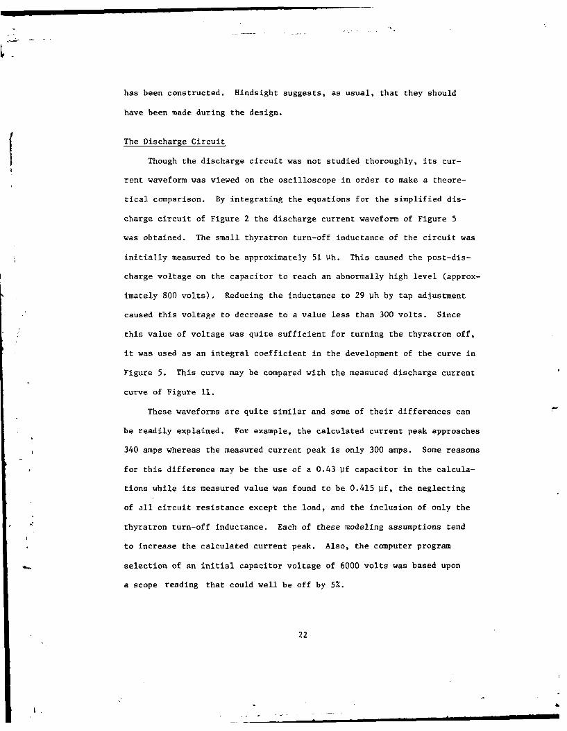
curve of Figure 11.
These waveforms are quite similar and some of their differences can
be readily explained. For example, the calculated current peak approaches
340 amps whereas the measured current peak is only 300 amps. Some reasons
for this difference may be the use of a 0.43 iif capacitor in the calcula-
tions while its measured value was found to be 0.415 pf, the neglecting
of all circuit resistance except the load, and the inclusion of only the
thyratron turn-off inductance. Each of these modeling assumptions tend
to increase the calculated current peak. Also, the computer program
selection of an initial capacitor voltage of 6000 volts was based upon
a scope reading that could well be off by 5%.
22
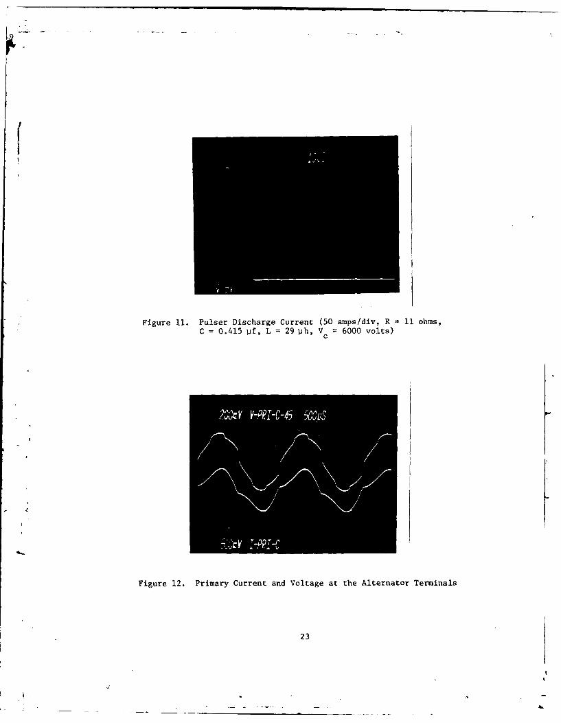
Figure 11. Pulser Discharge Current (50 amps/div, R = 11 ohms,C = 0.415 paf, L = 29 lih, VC 6000 volts)C
Figure 12. Primary Current and Voltage at the Alternator Terminals
23
The second difference in the waveforms is in the time to the cur-( rent zero crossing. The calculated waveform shows a half period of only
15 iisec while the experimental value approaches 19 Ijsec. Correcting the
capacitance to the smaller value tends to decrease the calculated half
period even further. However, an increase in the circuit resistance and
inductance due to the various components, such as the thyratron, tend to
increase the half period. Thus, a correction in the circuit resistance
and inductance appears to override the slight change in capacitance in
regard to the discharge waveform.
The ChargingCircuit
Alternator Terminal Measurements of Voltage and Current. Various
measurements were made at both primary and secondary points for the cir-
cuit of Figure 8. The current and voltage waveforms at the alternator
terminals were needed to help determine the impact of resonant loading
on the power source. The oscillograi of Figure 12 shows the primary
current and voltage at the alternator terminals with the system operating
at a speed of 2250 RPM (450 Hz) and excited to an output power level of
45 KW. All system measurements were taken with a constant DC voltage
applied to the exciter field since a satisfactory voltage regulator was
not available for this function.
Though some differences may be noted, the general appearance of the
waveforms is sinusoidal. This was, in particular, expected for the
voltage waveform. It contains a number of abrupt changes which are due
to the turning on of the diodes in the pulser. Note that there are six
transients per cycle. This number corresponds to the number of diodes.
The two largest transients occur near the C phase voltage zero crossing
and reflect the turn on of the two diodes in this particular phase. Any
24
time a diode in one phase turns on it disturbs the resultant armature
reaction flux and, thus, the resultant air gap flux. This disturbancef affects all phases, especially the phase containing the diode that turned
on. One other point to be noted is that the voltage does not experience
any sagging as the current rises to a peak. This was one of the problems
reported by Lt Silva in his investigation of DC resonant charging (Ref 8:
32-36).
The current waveform in Figure 12 presents the typical tsint shape.
Recall from equation (4) that the theory predicted this type of waveform.
Though not pictured, the waveforms for 15, 30, and 60 KW had the same
general appearance as those shown in Figure 12.
Pulser Measurements. Figure 13 shows the charging current and volt-
age waveforms for one of the two charging circuits of Figure 4. The mea-
surements were made at a point between the diode and the 0-5 amp ammeter.
The machine was delivering approximately 20 KW at 2200 RPM (440 Hz). As
in Figure 12, the half cycle charging current waveform displays the basic
tsint shape. The general form of this curve compares favorably with the
calculated charging current curve in Figure 9. However, these curves
cannot be compared on a magnitude basis since a value for the driving
voltage is assumed in Figure 9 but is unknown (and cannot very easily be
determined) for the oscillogram.
The charging voltage waveshape in the oscillogram closely resembles
the VC curve in Figure 10. However, the calculated voltage values in
Figure 10 have been referred to the transformer primary. This, plus the
problem concerning the unk~nown internal emf, means that the two voltage
waveforms cannot be compared on a quantitative basis.
25
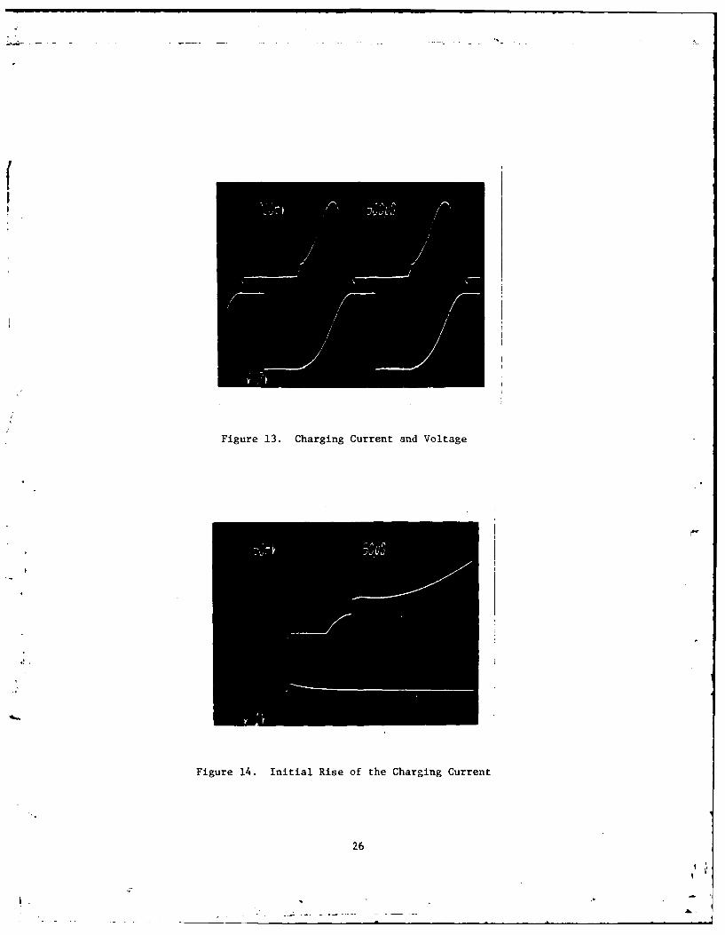
Figure 13. Charging Current and Voltage
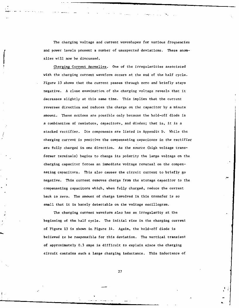
Figure 14. Initial Rise of the Charging Current
26
The charging voltage and current waveshapes for various frequencies
and power leviels present a number of unexpected deviations. These anom-
alies will now be discussed.
Charging Current Anomalies. One of the irregularities associated
with the charging current waveform occurs at the end of the half cycle.
Figure 13 shows that the current passes through zero and briefly stays
negative. A close examination of the charging voltage reveals that it
decreases slightly at this same time. This implies that the current
reverses direction and reduces the charge on the capacitor by a minute
amount. These actions are possible only because the hold-off diode is
a combination of resistors, capacitors, and diodes; that is, it is a
stacked rectifier. Its components are listed in Appendix D. While the
charging current is positive the compensating capacitors in the rectifier
are fully charged in one direction. As the source .(high voltage trans-
former terminals) begins to change its polarity the large voltage on the
charging capacitor forces an immediate voltage reversal on the compen-
sating capacitors. This also causes the circuit current to briefly go
negative. This current removes charge from the storage capacitor to the
compensating capacitors which, when fully charged, reduce the current
back to zero. The amount of charge involved in this transfer is so
small that it is barely detectable on the voltage oscillogram.
The charging current waveform also has an irregularity at the
beginning of the half cycle. The initial rise in the charging current
of Figure 13 is shown in Figure 14. Again, the hold-off diode is
believed to be responsible for this deviation. The vertical transient
of approximately 0.3 amps is difficult to explain since the charging
circuit contains such a large charging inductance. This inductance of
27
approximately 0.3 henries (referred to the secondary) should eliminate
any high di/dt component. The rounded portion of the initial current
rise seems to be caused by the resonating effect of the charging induct-
ance with the compensating capacitors in the rectifier stack. These
components produce a response which reaches a peak in approximately 35.7
ptsec. Though this value is quite different from the 50 llsec oscillogram
time, it seems to be a reasonable method for analyzing the current
initiation.
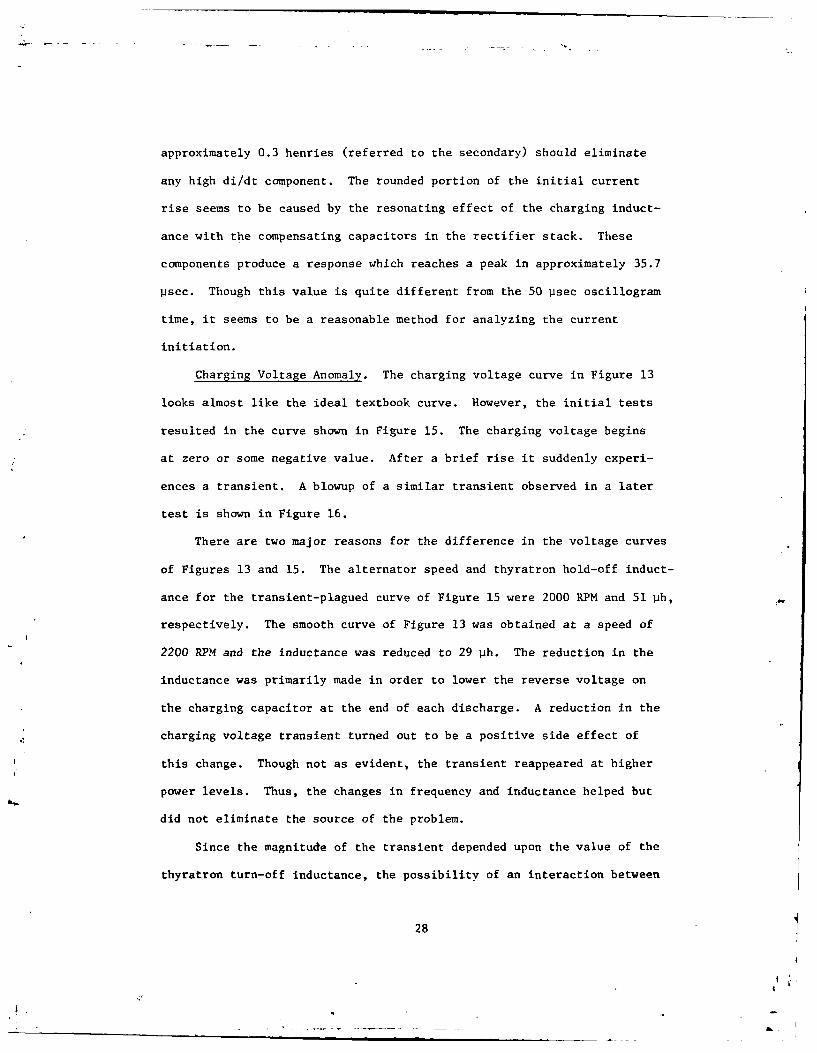
Charging Voltage Anomaly. The charging voltage curve in Figure 13
looks almost like the ideal textbook curve. However, the initial tests
resulted in the curve shown in Figure 15. The charging voltage begins
at zero or some negative value. After a brief rise it suddenly experi-
ences a transient. A blowup of a similar transient observed in a later
test is shown in Figure 16.
There are two major reasons for the difference in the voltage curves
of Figures 13 and 15. The alternator speed and thyratron hold-off induct-
ance for the transient-plagued curve of Figure 15 were 2000 RPM and 51 pih,
respectively. The smooth curve of Figure 13 was obtained at a speed of
2200 RPM and the inductance was reduced to 29 pIh. The reduction in the
inductance was primarily made in order to lower the reverse voltage on
the charging capacitor at the end of each discharge. A reduction in the
charging voltage transient turned out to be a positive side effect of
this change. Though not as evident, the transient reappeared at higher
power levels. Thus, the changes in frequency and inductance helped but
did not eliminate the source of the problem.
Since the magnitude of the transient depended upon the value of the
thyratron turn-off inductance, the possibility of an interaction between
28
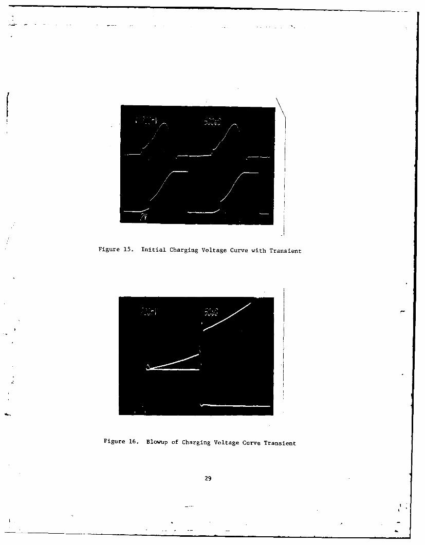
(m
Figure 15. Initial Charging Voltage Curve with Transient
Figure 16. Blowup of Charging Voltage Curve Transient
29
I I
the charge and discharge circuits of the phase was investigated. The
charging voltage curve for one circuit of the phase was observed after
disconnecting the external trigger input to the thyratron grid in the
second circuit. This effectively removed the second circuit from the
phase. When this was done the transient was eliminated.
Thus, it appears that the problem stems from voltage spikes produced
by the thyratron turn-off inductance in each discharge circuit. In order
to analyze the interaction between the circuits the schematic diagram of
the pulser has been simplified as shown in Figure 17. The circuit analysis
may begin by assuming that Cl has been fully charged and is awaiting dis-
charFe through thyratron Ti. The charging of C4 has just begun. Thus,
CR1 is turned off and CR4 is turned on. If T1 is now triggered to close,
CR I CR4 _
LL4
CC L I C 4 --4 + L 4
TT4
Figure 17. Simplified Pulser Schematic for Studyingthe Charge/Discharge Interaction
the discharge current through it causes the voltage on Ll(VLl) to go
positive and then negative. As the current approaches zero this
reversed polarity voltage reaches a magnitude that exceeds the slow
30
rising voltage on capacitor C4. (It also exceeds the source voltage.
( However, the charging inductance, LC, completely isolates the source
from this transient.) When the voltage on C4 is exceeded, CR1 turns on.
The charge which would have gone into building up additional reverse
bias on Cl is now shunted onto C4. The current path for this charge is
Ll, Tl, R4, C4, CR4, and CR1. When the discharge current passes through
zero, switch T1 opens, V Ll drops back to zero, and the transient ends.
From the transient standpoint it would be sufficient to remove Ll
and L4 from the circuit. However, they are required in order to assure
the turn-off of the thyratrons. Thus, for this particular pulser the
symptom, rather than the cause, must be addressed. One approach is to
incorporate an SCR in series with each rectifier stack. The trigger
timing should allow the SCR to turn on only during the charging half
cycle. Therefore, even if the transient should forward bias the SCR,
it will not turn on and, thus, the voltage spike due to LI will have no
effect on the C4 charging branch. This method does, unfortunately, make
additional requirements for hardware and triggering.
Readjustment of the thyratron trigger control box settings is another
approach that may be taken to resolve the voltage transient problem. The
firing mechanism should allow the voltage on the storage capacitor (C4) to
exceed the inductor voltage spike at the time of discharge. This means
that capacitor Cl must be discharged at a later time during the half
cycle. Thus, the new settings should prevent the turn-on of the diode
in the discharge branch since it will always be reverse biased. The
settings presently initiate the discharge when the source voltage reaches
a particular amplitude during the negative half cycle.
31
Many questions were left unanswered concerning the voltage and cur-
rent waveform anomalies. They were investigated primarily to gain a
qualitative understanding of their underlying causes. However, any
further examination was considered to be beyond the scope of this study.
Reso ince Determination
Including all of the system charging inductance in the alternator
could possibly reduce the power source weight by as much as 1/3 (Ref 6).
This would remove the necessity for the high leakage transformer which
was used in the MERADCOM charging circuit. In an operational system a
pulse transformer between the PFN and load cou'd provide any additional
voltage multiplication needed for the discharge pulse. Before the trans-
former leakage inductance can be incorporated into the alternator its
internal inductance for the AC resonant mode should be determined. It
is the combination of these two inductance that must then be designed
into the igh reactance machine. However, determining the internal
inductance, La9 turns out to be a difficult task.
There is a tendency to use classical steady state theory for deter-
mining La . The initial step is to find the resonant frequency, Wo"
The inductive and capacitive reactances should be equal at this fre-
quency. Thus,
XL = XC (7)
or
Lc /(2 CN) (8)
where
32
L C= total charging inductance
C N = network charging capacitance
Since L cconsists of the internal alternator inductance plus the trans-
former leakage inductance, L x, then L a nay be written as
La =LC -Lx(9
The difficulty with the above approach is that classical steady
state resonant theory is not applicable. A popular circuit analysis text
states, "Resonance, by definition, is fundamentally associated with the
forced response since it is defined in terms of a purely resistive input
impedance, a sinusoidal steady state concept" (Ref 3:450). The response
of the MADCOM system for half cycle charging includes both a forced
and a transient component. This is evident from the exponential terms
in equations (2) and (3). Thus, the system never reaches steady state in
the classical sense. This means that the system input impedance never
becomes purely resistive. At the beginning of each half cycle the source
11sees" the same input, a larLge inductor in series with a capacitor charged
to a slightly negative value. If the blocking diode of Figure 7 was
removed, a number of half cycles of charging would be required to get
the system past the transient state. Only then would the impedance be
resistive and the output waveforms sinusoidal. With the present system
configuration only the input is sinusoidal and even it is slightly
deformed by the turn-on of the diodes. Therefore, since the source never
"1sees" past the first half cycle, it continuously faces a circuit which
contains some reactance and has a transient response. Thus, equation (7)
is never realized.
33
In most resonant circuits a number of parameters can be varied
until resonance is detected. For example, changing either L, C, or the
frequency f should yield the circuit response needed to obtain resonance.
However, the frequency is usually chosen as the variable parameter. Re-
gardless of the selected variable, the source terminal voltage is main-
tained constant. This provides the standard from which measurements can
be evaluated. For example, resonance in the typical series RLC circuit,
as shown in Figure 7 with the diode removed, is obtained by holding the
source terminal voltage (point B) constant and varying f until a peak
current is reached. This occurs when the circuit becomes purely resis-
tive, that is, when the inductive and capacitive reactances cancel as
expressed in equation (7). When this happens a power factor of unity
may be measured at the source terminals and the current will be in phase
with the terminal voltage.
The nature of this research effort removes the constant terminal
voltage standard since part of the charging inductance is inside the
alternator. It is -.tow desired to hold the voltage at point A of Figure
7 constant and vary f until the peak current is reached. Also, this
current should be in phase with the voltage at point A. L a is assumed
to be approximately constant and C is fixed. The difficulty with this
procedure is that Ea the internally generated emf under load, is inac-
cessible. If it could be measured it would be a simple task to keep it
constant by varying the excitation.
The exciter circuit for the charging system is shown in Figure 8.
The circuit enclosed in the dashed block rotates at the same speed as
the rotor. It produces a flux which is then conditioned by the armature
reaction. The resulting flux then induces the alternator voltage Ea
which is approximated in the following equation.
34
E a= 4kN~f (10)
( where
k = form factor to account for non-sinusoidal aspects
N = number of turns linked by the flux
S= peak amplitude of the resultant flux
f = impressed frequency in Hz
Although equation (10) shows that E ais a function of and f it does
not infer that is itself a function of f. This is the case, however,
since an increase in f leads to an increase in the alternator field
current for constant exciter current. The field flux is then boosted
due to this larger current. Thus, the total change in E results nota
only from the increase in frequency but also from the variation in flux
due to the frequency change.
From the previous discussion it appears that there is no direct
method for determining resonance and, hence, L a- Thus, an indirect
approach was taken which may be used to approximate La
At unity power factor (behind the machine inductance) E ashould not
be much greater than the terminal voltage V T and can be calculated if a
value for L ais assumed. Since E acannot be measured, this one value is
of little help. However, if E a is calculated for a number of frequencies
and is them divided by the measured current I for these same frequencies,a
an impedance trend (Z versus f) is developed. This procedure was followec
for a number of values for L a- The goal was not to determine the fre-
quency at which the impedance became purely resistive but rather the fre-
quency at which it became a minimum. As indicated earlier, the circuit
is in a transient mode and its input impedance will always be somewhat
reactive. The equation used to calculate E a was
35

wher E = internally generated emf (volts rms)a
T = alternator terminal voltage (volts ins)
I a= phase current measured at the alternator terminal (amps rms)
anlbeweVTanEa(dges
6= angle between VT and Ia(degrees)
R a= 0.27 = internal phase resistance of the alternator (ohms)
W= alternator frequency (radians/second)
L a=selected alternator internal inductance (henries)
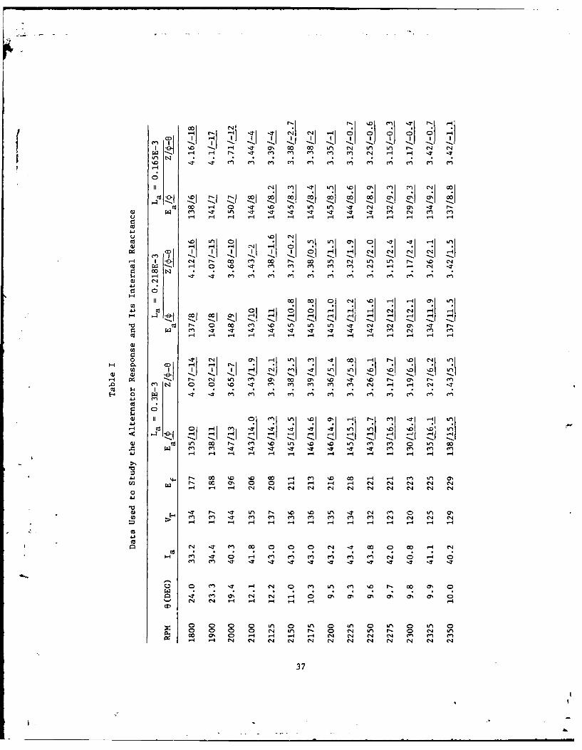
The various parameters and values which were associated with equa-
tion (11) are listed in Table I. All measurements were taken with the
generator field current held to a constant value of 8.0 amps. A number
of values for La were selected and evaluated. However, only three are
listed in the table. The first value selected was 0.218 mh, the speci-
fication sheet leakage inductance. As the frequency was varied the
impedance Z reached a minimum at 2275 RPM. Although this may indeed be
the frequency at which the minimum impedance occurs it is also the fre-
quency at which the system started to become slightly unstable. It is
believed that the 60 KW tests caused some problems in the switching cir-
cuits. There was insufficient time to try to correct this problem and,
thus, some instability was noticed at the higher speeds.
As noted above, the choice of 0.218 mh for L a resulted in a minimum
impedance at 2275 RPM or 2859 rad/sec. This frequency can now be sub-
stituted into equation (12) to determine the validity of the L aselection.
[1 (c21/a C -n)1l/ (12)
c N c
36
W, 0 0 0-4
'0 m~ -cn Cl) Cn cn en~ Cn m Ce
0
Cu co 'A4 0 %4 0 114 L(n Lrn .4 (N (N 6 r-.(Ii IT Cn '1U~.4 .01 .4 'T .r IT en mN C~cn
u .- - '4- 4 1-4 - -1 1-4 .-4 1-- 4 -4 -4
Cu IDL 0* L
Im 0
A-II
C;
I. -- -* I. - -
Cu r- 0 Co cn '.0 tn un Ln cq P,( ' 4 r
ca ~ -4 1 4 v-4 -4 -4 1-4 - -4 14 -4 '- '1 -
en N~ '. 0. L0A c l 4 - 4 -
- -4
Cu~~ A-
w-. 0- Go ON .4 1-4 1-1 A A C C C-4 "A C-4a C4
0) Cu LA C I- Ln '0 %D %.D '.M l mA C LM ONm mA CA r - n .4 en m4 .4 m4 .4 "4 "A CN4-I-4 -4 .4 .- 4 ,4 - -4 -4 r4 1-4 1-1 .-1
4-I
(n -co. 4 L C 0 '0 C1 4 (Nt c 0 00 -4 'lHu to V4 C4 _; &; C4 C4 (A (4 _; (N (N (N4 (
-4 -4 -4 -4 -4 -4 -4 4 - 4 -4 - 4 -CD
(N 0 C o 0N 0n 0 (N .4 L 0l o V%(0-4 ON 0 -4 -4 -4 14 04 C4 C4 (N M en 0_q CA 4 .4 V4 .4 .4 .4 4 .4 .4 04 .14 04
e 0 CA 4 ( 0 CA A C ' C- Co37
where
R = 0.445 = total charging circuit resistance (ohms) and the
remaining terms have been previously defined. This equation, when solved
for L , yields
L= 1 1 2 ()2]1/2 (13)c 2 +a2- (13)
2w aCN Wa CN a
Upon substituting COa= 2859 rad/sec, CN = 142 Pf, and R = 0.445 ohms
into equation (13), Lc is found to be 0.855 mh. Subtracting the trans-
former inductance of 0.69 mh from this gives a value for L of 0.165 mh.a
This value may now replace the initially selected value of 0.218 mh
for L . With this new value E and Z are calculated for varying fre-a a
quencies. As Table I shows, the minimum Z (both magnitude and angle)
occurs at 2275 RPM. (The calculated angle cannot be viewed quantita-
tively.) This same speed resulted for each selection of L . Thus, the
alternator supplies an internal inductance of approximately 0.165 mh at
a resonant frequency of 455 Hz. However, the data in the last column
of Table I implies that the "resonant bandwidth" may be quite wide.
Since the alternator waveforms are similar to sinusoids, the bandwidth,
as with steady state theory, should depend upon the Q of the circuit.
This factor is relatively low (approximately 5) and, therefore, supports
the conclusion of a wide bandwidth.
The value of Xa, determined from La, may now be compared with the
values of reactance found in the alternator specifications sheet. For
this comparison it is transformed into its per unit reactance value.
This is accomplished by the following equation
Xa 27rfLa/(VB/IB) per unit (pu) (14)
38
I.
where
f = 400 =design frequency (Hz)
' VB = 240 =base voltage (volts)I= 26 =base current (amps)
Substituting these values and L a =0.165 mh into equation (14) gives a
value of 0.0449 pu for X a. The only reactance value in the specification
sheets that is in this magnitude range is the armature leakage reactance.
Its value is 0.0594 per unit. Thus, the value for X aappears to be
slightly lower than the leakage reactance value.
The alternator should respond differently for a transient condition
and a steady state operation unless the transient is of such a nature
that it is viewed by the machine as steady state. As explained earlier,
half cycle charging produces a transient response. So now the point of
interest is how this particular transient response impacts the operation
of the alternator. A second use of the measured data in Table I may be
made in order to investigate this point. The data will be applied to the
two-reaction method for computing the angle ip between the phase current
la and the open circuit voltage Ef (Ref 1:114; 7:204-212). The steady
state reactance components will be used in conjunction with this data in
order to develop the vector diagram drawn in Figure 18. The two-reaction
method assumes steady state operation. Thus, if the approach is still
applicable using the measured data then it strongly suggests that the
alternator views the system operation as steady state (nearly sinusoidal).
The following equations will also be useful in this development.
39
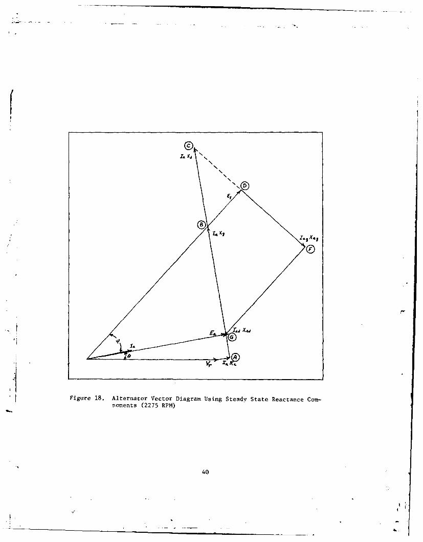
I, x0
Figure 18. Alternator Vector Diagram Using Steady State Reactance Comn-I ponents (2275 RPM)
40
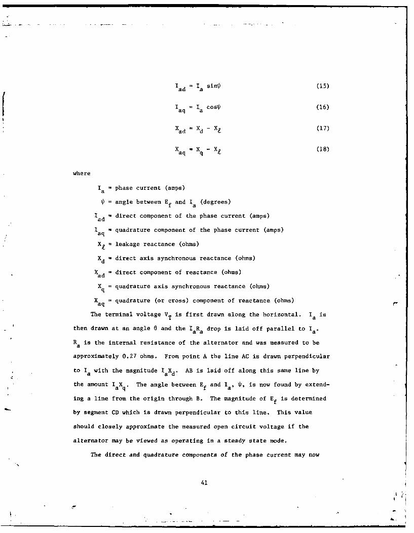
'ad = Ia sinP (15)
Iaq = Ia cos (16)
Xad - Xd - Xt (17)
Xaq - Xq - Xt (18)
where
I = phase current (amps)a
= angle between Ef and Ia (degrees)Iad =direct component of the phase current (amps)
I = quadrature component of the phase current (amps)aq
Xl = leakage reactance (ohms)
Xd direct axis synchronous reactance (ohms)
Xad - direct component of reactance (ohms)
X = quadrature axis synchronous reactance (ohms)q
Xaq = quadrature (or cross) component of reactance (ohms)
The terminal voltage VT is first drawn along the horizontal. Ia is
then drawn at an angle e and the laRa drop is laid off parallel to Ia-R is the internal resistance of the alternator and was measured to bea
approximately 0.27 ohms. From point A the line AC is drawn perpendicular
to Ia with the magnitude IaXd. AB is laid off along this same line by4a
the amount I aX q . The angle between Ef and Ia is now found by extend-
ing a line from the origin through B. The magnitude of Ef is determined
by segment CD which is drawn perpendicular to this line. This value
should closely approximate the measured open circuit voltage if the
alternator may be viewed as operating in a steady state mode.
The direct and quadrature components of the phase current may now
41
I.°
be used to. find the internally generated voltage, E a- This is begun by
first extending a line from point D to point F. It is parallel to CD and
has a magnitude I aqX aq. The vector I adX adis then drawn perpendicular to
this line. It begins at point F and should terminate at some point G on
line segment A.B. The vector for the internally generated voltage E amay
then be drawn from the origin to G. The final vector of interest connects
points A and G and should have a value I XV~
Many cystem transients are of such a nature that they induce tran-
sient currents inside the alternator. For this case the synchronous
reactance values cannot be used in the development of the vector diagram
in Figure 18. A use of these values would cause the diagram to be in
error. Most notable, E f would be incorrect in magnitude and direction
and, hence, would not equal its measured value.
Under certain circumstances the operation of the alternator may be
viewed as steady state even though it feeds a circuit experiencing a
transient response. Apparently, this is what is happening during AC
resonant charging and, thus, the use of the synchronous reactances in
the development of the alternator vector diagram is permissible.
There are a number of reasons the alternator may be considered to
be operating in the steady state. At the beginning of each charging half
cycle the circuit connected to the alternator terminals is changed. Just
before this half cycle begins the source is completing the build-up of
peak charge on one capacitor. At the completion of this build-up the
charged capacitor circuit is replaced with a circuit containing a capa-
citor holding a slightly negative charge. This new circuit results in a
mathematically transient response (see equation (2)). However, the
response is so gradual (primarily due to the large charging inductance)
42
that the alternator can barely distinguish it from 400+ Hz operation. As( shown in Figure 12, it contains no current discontinuities at the half
cycle end points or during the charging of the capacitor. The smooth
transition at the end points is primarily due to the initial condition
requirements. These are specified in Appendix A which shows that the
current must be zero at both the beginning and end of a half cycle. All
of these characteristics combine to produce a repetitive waveform at the
alternator terminals and an armature reaction that is fixed both in magni-
tude and direction with respect to the poles. The fixed nature of the
armature reaction prevents the build-up of the voltages which cause
transient currents inside the machine (Ref 5:286-290). Thus, synchronous
reactances may be used in developing a two-reaction alternator vector
diagram as shown in Figure 18. The vectors drawn in this diagram were
based upon Table I measurements taken at 2275 RPM and the synchronous
alternator reactances listed in Appendix D. The diagram results in an
open circuit voltage of 215 volts. The terminal point of the I ada
vector is slightly past lime AB. The distance from this point to A is
measured to be approximately 24.6 volts which results in a value for X
of 0.064 per unit. This per unit value is just slightly larger than the
0.0594 leakage reactance value specified for the alternator. Similarly,
the graphical value of E f is 6 volts less than the measured value of 221
volts. These differences are well within the realm of error in measure-
ment. The results indicate that although half cycle charging is a
transitory condition it allows the alternator to experience a mode of
operation that very closely resembles steady state.
43
IV. Conclusions and Recommendations
There were a number of objectives associated with this study. One
of the most important was to determine the impact on an alternator when
it operates in the AC resonant charging mode. Its output waveforms were
to be analyzed for degradation while .,-aryi ng the load and frequency. The
final objective was to determine, if possible, when the system was at
resonance. This was equivalent to determining the internal reactance of
the machine.
Conclusions
The system was successfully tested for 15, 30, and 45 KW. However,
only a few measurements were taken at the 60 KW level due to the develop-
ment of trigger circuit problems. These load variations did not cause
any noticeable degradation of the alternator operation. A similar con-
clusion was reached when the frequency was varied from approximately 380
to 475 hertz. This, to some extent, results from a low circuit Q of
approximately 5.
Although a number of anomalies were detected in the charging wave-
forms, the waveshapes very closely conformed to the theoretical predic-
tions. The anomalies were found to be peculia;: to the hardware and con-
figuration of the system under investigation.
During the latter tests, system noise tended to aggravate the
trigger circuits and caused pre-firing of certain thyratrons that must
have been adversely affected during the 60 KW tests. Reducing the gas
pressure inside the thyratron tubes could have possibly alleviated this
condition.
44
( No straightforward method was developed for determining precise
resonance. The term resonance as used in this study context is some-
what of a misnomer since classical steady state resonant theory is not
really applicable. Classical theory addresses only the forced response.
This study showed that the transient response cannot be excluded.
Classical theory also seeks a maximum amplitude response when all
reactances cancel and the system is purely resistive. This study con-
cludes that the half cycle charging circuit has a transient response.
The reactances do not completely cancel and, thus, the input impedance
is never purely resistive. Even so, the alternator armature reaction
is approximately fixed, both in magnitude and direction, with respect
to the poles. This implies that the alternator is in a near steady state
mode of operation. This latter point was confirmed by the use of measured
data and synchronous reactances in a two-reaction vector analysis for the
alternator. This same data was used to determine the internal reactance
of the alternator during resonant charging. It was found to be slightly
less than the armature leakage reactance.
Recommendations
The literature search for this study led to the conclusion that there
is only scant material on charging systems. Thus, an investigation of
methods other than AC or DC resonant charging would contribute to filling
this void. One method, in particular, which has caught the interest of
the Army (MERADCOM) is network charging. This method limits the peak
current requirements and is not expected to cause as negative an impact
on the alternator as does DC resonant charging. Further, its controls
and triggering should be simpler than those needed for AC resonant
charging. It needs to be investigated and compared with the methods
already studied.
45

The AC pulser is a very basic prototype. The MERADCOM engineers
were aware of many of its shortcomings before its delivery. If these
design problems could be corrected this would permit more reliable and
expanded testing. In addition to redesigning the trigger controls, con-
sideration would have to be given to wiring, grounding, noise suppres-
sion, and the general physical layout of the circuit.
46

Bibliography
1. Bailey, Benjamin F. and James S. Gault. Alternating-Current Machinery.New York, Toronto, and London: McGraw-Hill Book Company, 1951.
2. Glasoe, G. N. and J. V. LeBacqz. Pulse Generators. New York andLondon: McGraw-Hill Book Company, 1948.
3. Hayt, William H., Jr. and Jack E. Kemmerly. Engineering CircuitAnalysis. New York, San Francisco, Toronto, and London: McGraw-Hill Book Company, 1962.
4. Kuhlmann, John H. Design of Electrical Apparatus (Third Edition).New York: John Wiley and Sons, 1950.
5. Lawrence, Ralph R. and Henry E. Richards. Principles of Alternating-Current Machinery (Fourth Edition). New York, Toronto, and London:McGraw-Hill Book Conpany, 1953.
6. O'Loughlin, James P. Electrical Engineer, Air Force Weapons Laboratory(personal interview). Kirtland AFB, New Mexico, June 16, 1981.
7. Puchstein, A. F., T. C. Lloyd, and A. G. Conrad. Alternating-CurrentMachines (Third Edition). New York: John Wiley and Sons; London:Chapman and Hall, Limited, 1958.
8. Silva, Jaime R. "Prime Power to Pulse Conditioning Interface Methods."MS Thesis. School of Engineering, Air Force Institute of Technology,Wright-Patterson AFB, Ohio, December 1980.
9. 75-11605, Addendum 2. "Subsystem Design Analysis, Lightweight Alter-nator (Model Test Program)." Preliminary Final Report prepared forthe Air Force Special Weapons Center, Kirtland AFB, New Mexico.Torrance, California, Airesearch Manufacturing Company of California,June 30, 1976.
47

Appendix A
Theoretical Development of the
AC Resonant Charging Equations
48
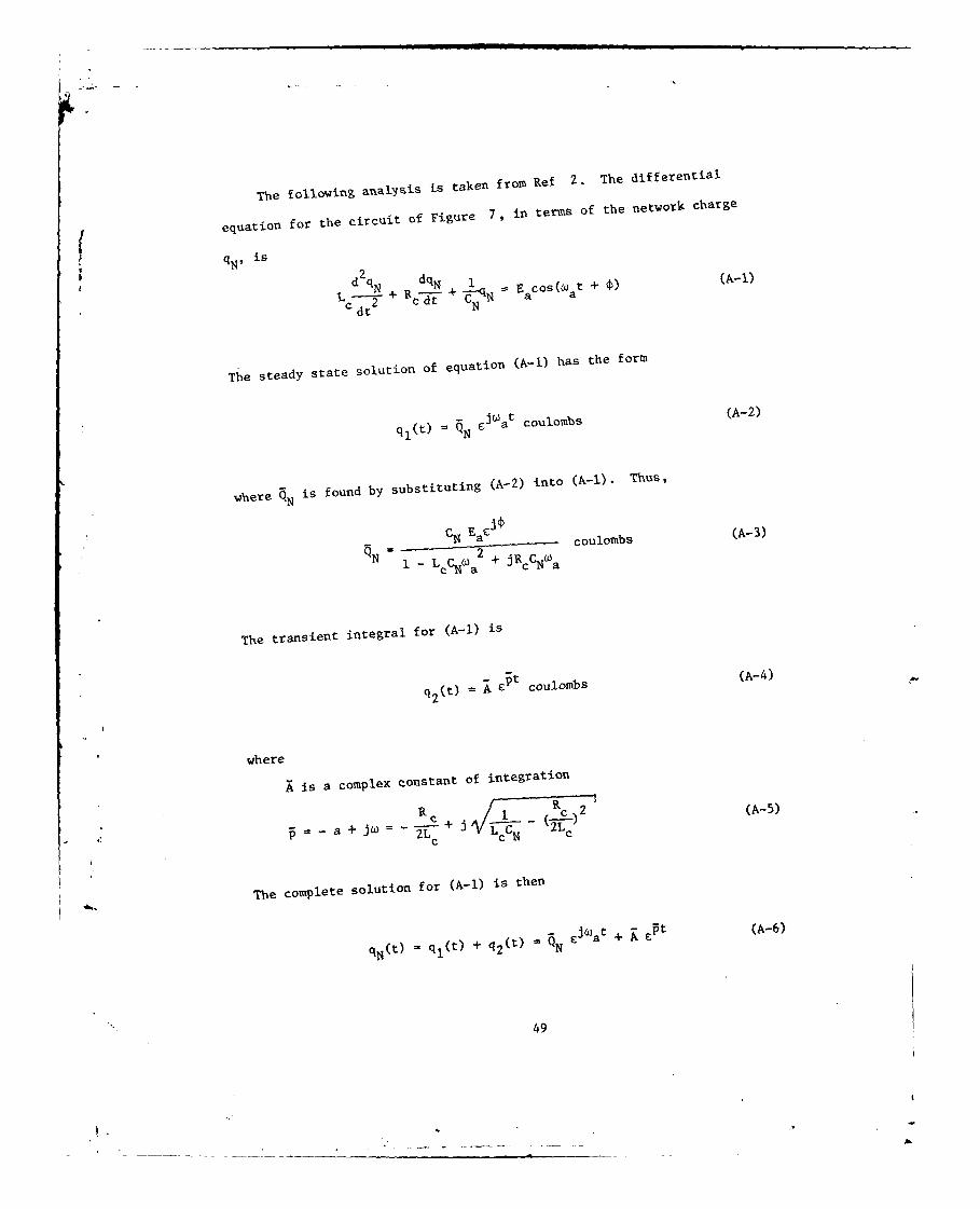
The following analysis is taken from Ref
2. The differential
equation for the circuit of Figure
7, in terms of the network charge
qNs is
2d qN dqN 1 ECOS (A-l)
L +P,- -- q a aw+~
~dt 2 ct CN a
The steady state solution of equation (A-I)
has the form
ql(t) N cjuat coulombs (A-2)
where &N is found by substituting (A-2)
into (A-I). Thus,
CN 2Eac coulombs (A-3)
1 - LC a2 + JR cCNa
The transient integral for (A-I) is
q2(t) C p
t coulombs (A-4)
where
A is a complex constant of integration
+c j L R) (A-5)
a + j w c 2LL
The complete solution for (A-l) is then
qN(t) ql(t) + q2 (t) -N cJat + F Pt (A-6)
49

For the general case the following initial conditions
at t 0 may be
assumed
( qN(t) = qN(O)
ic (t) = i c(0)
Substituting these values into equation (A-6) and the
time derivative
of (A-6) gives
qN(O) = Re(QN + Q, + A1
i (0) = Re(jwaQN + A) = -aQ2 -A -A 2
Solving for A1 and A2,
(A- 7)
Al qN(O) -Q
S{i(0)+LQ +_ QO (A-B)
c -
where the abbreviation "Re" means "real part of".
Now let
A = = IA I + JA2z
A2
= phase angle of A arctan A1iI
1 Ioi + jQ21
phase angle of circuit = arctan--I - L cCN°Ja
50
• a . .
Thus, equation (A-3) may be written as
D QN = QN - (A-9)
The solution for qN(t) may then be written
qN (t) = Re( N EJWat + A Pt)
qN(t) = QNCOS(Wat + 6 - ) + A C-atcos(,t + p) (A-10)
Now, differentiating (A-10)
i C(t) = OaN{-sin(at + - e))+ A{-_-at wsin(t + )-a C-atcos(t + )
oror
-ato(t)S(at + = - 0 + E) + o AE cos(t + + B) (A-Il)
c aN(at 2 0
where
-=N CN Ea
1 Lc CNWa + RcCN wal 1-2
= angular frequency of circuit
= arctan-a
0
For AC resonant charging the circuit frequency, W, is set equal to
the impressed frequency, w a With w = w equation (A-10) becomesa a
51
.1

qN(t) = QNCOS(&)at + - e) + A -atcos(, at + p) (A-12)
f Expanding cos(W at + f) and recognizing that A1 = Acosp and A2 = Asin*
(A-12) becomes
qN(t) = QNSin(Wat + V) + J-at[A 1cosat - A2sinwat]
A1 and A2 in this equation can now be replaced with the right side of
equations (A-7) and (A-8). Making these changes and substituting QNsin
for Q and QNcos4 for Q2 yields the equation for the network charge
qN(t) _ QN(I _ -at )sin(W at + 0) + t-atq N(O)cOS at +
i (0) aqN(0)c + a - 7 N sin )sin at) (A-13)
a a a
The condition for repeating transients is, for half cycle charging,
i c(7) + i (0) = 0. The current is now obtained by differentiating equa-
tion (A-13) and is
Ea -atE (t) -A (I - c-at)COS(Wat + 4
c R cac
E+ -at(i c(O)COS a t - Wa qN (0)sin a t + 2L-- c- in a t Cosca
E
L -at, sin- i(0) - aqN(0)} sinat (A-14)a ca
~Ewhere a-has been substituted for QN'
ca
At wat 7r equation (A-14) becomes
52
a "a O ira~ 1 aC5 a i ca i(o) = -
Solving for i (0) yields
E1 (0) = - cos(c C
The quality factor Q is defined as
Lc a 1 (A-16)
Cc aQ --F-- = RcC N~a
By substituting i (0) and Q into (A-13) a revised equation
for the net-
C
work charge is obtained
W ta
qN(t) = Q CNEa (1 - 2 )sin(Nat + 4)
W It C E1a - N a sin 2N ( ) ) siratI
+ C Q { q k(0 )c oS U) t + ( Q C N a Sc ) - - n + ( 1)(A-17)
This equati"m is then differentiated to produce the charging current,
W ta
ic(t) QCNEaia (I - F- -Q)cos kwat +
W at
+ - "2Q QCNEa% OS*coswt
qN(O) in) N(O) a (A-)N 1 , s irnwat) A-
" -N[CNEaW (- -a 4Q
This expression may then be restructured to give
53

_ I
0)t W ta a
ic(t) = QCNEa{(I - E 2Q)cor(6at + 0) + - 2Q [cOS~coswat
qN ( 0 ) ._1..1 _1 ino)sinwat]l (A-19)-(C- a(1 4- 4Q 2
which, for most values of Q, can be approximated by
W ta
ic(t) = QCNE awa{(I - c 2Q )cos(Wat + €)
a qN(O)+ c 2Q [cos~cOSiat - fEa-Sim atil (A-20)
Since it is generally more convenient to express an equation in terms of
voltage rather than charge, (A-17) may be revised using the transformation
V ( q/CN, that is,
VN (t) -a (Wat qN(N)
E = Q{( - - 2Q )sin(wa t + 4) + c 2Q I[QCN E- OS0atEa QN~a
+ (coso - qi + I q0) (A-21)2Q 2Q2 %EaSna]}A-1
If the losses in the charging circuit can be neglected then the
expression for the charging current, equation (A-20), can be further
simplified. This is done by taking the limit of I Ct) as Rc approaches
zero. After application of L'Hospital's Rule (A-20) becomes
54
h.t
E t= cos( C t + P) + i (0)cosw t
C'~ 2L a C aC
E
a+[ L a cos w qa qN0sinwat (A-22)
Thus, for half cycle charging
E ri = 2(a 2 aa cos + i(0)] (A-23)
ac cos c()
As stated earlier, the condition for repeating transients is i (Tr)
- ic(0). Therefore, the only solution for (A-23) is
cos = 0 or = ±2
and so, from (A-15)
i (0) = 0C
Equation (A-21) may be evaluated at the discharge point, w at = i,
to determine the resulting stepup voltage ratio
VN(7) IT q N(0)
= - [Q(l - C 2Q)sin + E e 2Q] (A-24)
If 7r/2Q << 1 then the exponentials in the above equation may be approxi-
mated using
Itc2Q~l2Q
and
55
IT
-c 2Q
Substitution of these expressions into (A-24) yields
v N T - sin) + _N_ (I_ (A-25)
E a -4 -Q2 )sik.C
Then for the case where there is no initial charge on the network and
the losses are negligible, (A-25) becomes
VN(r') E si (A-26)
E 2a
and, thus, for maximum network voltage
(A-27)2
56
* .* l

Appendix( B
I Program EQUATE
57A
PROGRAM EQUATE
I, l10=C THIS PROGRAM INCLUDES THE EQUAT10MS FOR THE CHARGING VOLTAGE
110=C AND CURRENT AT RESONANCE. THE SOURCE FOR THE EQUATIONS IS THE120)=C PULSE GENERATOR TEXT BY GLASOE A0D LEBACQZ. FOR COMPARI SON130=C PURPOSES T11E SOURCE AND INDUCTOR VOLTAGE EQUATIONS HAVE ALSO140=C BEEN INCLUDED. THE TIME STEP FOR, THE EQUATIONS HAS BEEN SET TO150=C IO.E-6. THE EQUATIONS ARE SOLVED AT THESE TIME POINTS FOR160=C A HALF PERIOD. RATHER THAN DISPLAYING THE OUTPUT ON THE170=C SCREEN, IT IS STORED ON TAPE8.130=C190=C200=C210= PPRO(AN GLASOEC INPUT,CUTPUT ,TAPE-5=1iNPUT,TAPE6=OUTP.UT,TAPE8)220= REAL LCICCMAX23o= REWIND 8240= P1=3.141592654250= RC=0.445260= LC=0.853E-3270= CN,=147.17E-6230= EA=150.0290= VCZERO=-5.4300= PHI=-PI/2.0310= A=RC/(2.0*LC)320= OMECAO=1 .0/SQRT(LC*CN)330= OMEGAA=SQRT(OMEGAO**2-A**2)340= PPM=OMEGAA/ (0 .4*pI)350= Q=OIIEGAA*LC/RC360= QCZERO=CN*VCZEPO370= FINTI:!=PI/OMEGAA380= T-0.0390= WRITE(6,3)400= 3 FORMAT(6X,411IME, 9X, 2HIC, 12X,211VC, 1OX,2HVL,LO0X,6HOllEGAA)410= 1 EX-EXP(-OxiEGAA*T/(2.O*Q))420= IC-Q*CN*EA*OMEGAA*( (1 .0-EX)*COSCOAIEGAA*T+PHII)430= #+EX*(COS( PHI )*COS(OMEGAA*T)440= # -(Q CZERO/(Q*CN4*EA)*C1.0-1.0/(4.0*Q**2))450= #-1 .O/C4.O*Q**2)*SINCPHI))*SIN(OMIEGAA*T)))460= VC-EA*O*( (1 .f)-EK)*SINCOM ,EGMV*T+PHII)+EX*470= #( QCZERO/ ((Q*C;'*EA) *COS (Ol EGAA*T)+480= (COs(PFiI)-1 .O/(2.O*Q)*SIN(PHIl)+1.O/(2.O*Q**2)*490= #QCZEFRO/(CN4*EA))*Slu:(O-,iEGAA*T)))500= V-EA*COS(OlMEGAA*T+P!]I)510- VL=V-RC*IC-VC
58
520= WRITC(8",2)T,IC,VC,VL,0M ECAA530-C wBITE(6,2)T,IC,VC,VL,OMIEGAA540= 2 FORt LAT(lX,E12.5,1X,E12.5,1X,E12.5 ,LX,E12.5 ,IX,E12.5)(550- 4 icliX=Ic T
580= REWIND8590= STOP
600= END
59

Appendix C
Operating Instructions and Listing for Program RKFOUR
Program RLCCHG
Program RLCDIS
60
Operating Instructions for RKFOUR
Programmer: B. D. Weathers
Purpose: RKFOUR is an integration routine designed to provide the
equivalent of an analog computer integrator for the solution
of normal-f orm differential equations.
Features
---An arbitrary number of integrators can be used. The number used is
determined by the size of the storage arrays set in the calling
program.
---All variables that affect the operation of RKFOUR appear in the
calling statement; multiple uses of the program are possible, but
care must be used to prevent time desynchronization.
---The independent variable step size is determined automatically, but
if desired this program can be made to run with a fixed step size.
---The adaptive step size feature, if used, will insure little trouble
with numerical instability.
---The limits on the adaptive step size may be set in the calling
program, or default values may be used.
---The error limits that determine when the step size should be changed
are program parameters, and hence may be externally controlled.
---An adjustable delay is available to prevent eratic step size
changing. Once the criteria is satisfied step size increases by
the appropriate factor at each time.
4 ---- Step sizes may be changed externally, but may not be changed in the
middle of an iteration, that is when KEEP is equal to 0.
61
A solution point counter is contained in the routine to enable
( termination if appropriate independent variable criteria is not
available.
Suggestions for Use
Before using this subroutine for the first time, a careful examina-
tion of the flow chart should be made. Also a thorough examination of
the program parameter should be carried out to insure that the default
values of the parameters will be satisfactory, if used.
You must set all non-zero initial integrator outputs. All non-unity
integrator gains must also be set in section 2.
The value for li(l) - Step Size - should be set as close to the pre-
dicted sampling interval as possible. This will insure a more efficient
operation for the first pass.
If running in "Open Shop" and the 20 second time limit is just a
"bit too short," add "R11N=NO CHECK" to the control card. Do this only
after your name, after you are SURE the program is free of programming
errors. On a large job this can add 15% to the available computation
time, by eliminating several compiler tests.
CALL RKFOUR (NINT, Y, X, GA, PE, XX, H, ZZl, ZZ2, ZZ3, TIME, PNTS, KEEP,
IFL)
NINT - Number of integrators. Storage for the integrators must be
defined in the calling program. There is no maximum, but
the example program is set for up to 20.
Y - An array that contains the integrator output. Default
initial values are zero.
X - An array that contains the integrator inputs.
62
GA - An array that contains constant gains associated with each
integrator. Default values are 1.0.
PE - A working array used to store absolute peak values of the
integrator outputs. This array is set to zero during initial
entry to RKFOUR.
XX - An array used in two ways. If I denotes the Ith integrator,
then XX(I,I) stores the past value of the integrator output
and XX(2,1) stores the past value of the integrator input.
During the integration cycle the XX(3,I) and XX(4,I) positions
are used to store the derivative values needed by the integra-
tion algorithm. At the end of a cycle, XX(3,I) holds the new
integrator output and XX(4,I) holds the new integrator input.
It is possible, with the values, to implement a third order
interpretation for the values of the integrator outputs
between steps. This would serve to offset the problem of
obtaining values at discrete time points and would be more
efficient than step size manipulation.
H Array - The integration control parameters.
H (1) - The current independent variable step size.
H (2) - Minimum permissible step size (Default value is 0.0).
H (3) - Maximum step size (Default value is 1.OE + 8).
H (4) - Factor used to modify the step size- must be greater
than 1.0 (Default value is SQRT of 2=1.414214).
H (5) - Proportional to the lower error bound (Default value
is L.0E - 4).
H (6) - Proportional upper error bound (Default value is
l.OE - 02).
63
H (7) - Adaptive step size control (Set to -1 for constant
step size operation) (Default value of 0.0 causes
adaptive step size operation).
H (8) - Delay in increasing the step size after error
criteria is met. (Default value is 3.0).
H (9) - Last value of the independent variable.
ZZl, ZZ2, ZZ3 - Working arrays used to store the constants
needed for the integration routine. These arrays are
TIME - The independent variable set within RKFOUR. The
default initial value is zero.
PNTS - The counter of permanent solution extensions. Use
this variable for termination when other termination
options fail.
KEEP - This variable is set to ONE only when the data in the
derivative evaluation section is permanent. It is
zero at all other times. This variable should be used
as a control upon memory dependent functions.
IFL - The IFLag array.
IFL(l) - Set to -1 at the first entry to RKFOUR, and is 0 at
the first exit. On subsequent exits it has a value +1.
IFL(2) - Has the value -1 to +3 depending upon where the inte-
gration routine is in its operation cycle.
IFL(3) - This flag is used to control the step size from the
derivative evaluation section of the calling program.
It is set to -1 for step size reduction, and +1 for
an increase in the step size.
IFL(4) - This flag is -1 when initializing calculations are to
64
be made. It is 0 when only the derivative evalua-
tion is required, and is +1 when the solution has
been successfully extended over one step of the
independent variable.
IFL(5) - This flag is set to +1 immediately after IFL(4) is
-1 for the first time. It is intended as a signal
for other routines that may be used that initializa-
tion is underway.
IFL(6) - This flag is used for the temporary storage of the
variable KEEP.
65
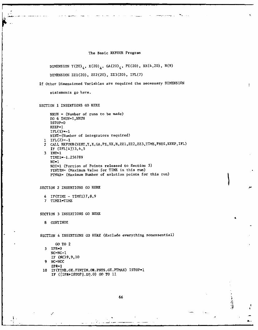
The Basic RKFOUR Program
DIMENSION Y(20) 4, X(20) 4, GA(20) 4, PE(20), XX(4,20), H(9)
DIMENSION ZZ1(20), ZZ2(20), ZZ3(20), IFL(7)
If Other Dimensioned Variables are required the necessary DIMENSION
statements go here.
SECTION 1 INSERTIONS GO HERE
NRUN = (Number of runs to be made)DO 6 IRUN=l,NRUNISTOP=OKEEP= 1IF(l)=-lNINT=(Number of integrators required)
1 IFL(2)=-l2 CALL RKFOUR(NINT,Y,X,GA,PE,XX,H,ZZl,ZZ2,ZZ3,TIME,PNTS,KEEP,IFL)
IF (IFL[4])3,4,53 INT=l
TIMEI=-l.256789NC=lNCC=l (Portion of Points released to Section 5)FINTIM= (Maximum Value for TIME in this run)
PTMAX= (Maximum Number of solution points for this run)
SECTION 2 INSERTIONS GO HERE
4 IF(TIME - TIME1)7,8,9
7 TIMEl=TIME
SECTION 3 INSERTIONS GO HERE
8 CONTINUE
SECTION 4 INSERTIONS GO HERE (Exclude everything nonessential)
GO TO 25 IPR=O
NC=NC- 1IF (NC)9,9,10
9 NC=NCCIPR-1
10 IF(TIME.GE.FINTIM.OR.PNTS.GE.PTMAX) ISTOP=lIF ((IPR+ISTOP].EQ.0) GO TO 11
66
.1
SECTION 5 INSERTIONS GO HERE
11 INIT=OIF (ISTOP)l,I,6
6 CONTINUEWRITE (6,100)
100 FORMAT (011, 1X)STOPEND
Basic RKFOUR System
There are a number of variables in the RKFOUR System whose value
depends upon the problem undertaken.
NRUN - The number of runs to be made.
NINT - The number of integrators to be used in the run (limited
to 20 by storage allocation in the stock system).
NCC - The portion of solution points that are released to the
output section (Section 5) NCC = 1 delivers every point,
NCC = 2, every second point, etc.
FINTIM - The maximum value that the independent variable will
attain. The program will terminate upon the first solu-
tion point to meet or exceed this value.
PTMAX - The maximum number of solution points in any one run.
IPNT - The point counter used in plot routines. It may be set
to 0 in one of two locations. If summary curves are
desired, set to 0, before the IRUN DO statement. If no
.4 curves are desired, set to 0 after the IRUN DO statement.
INIT - This variable is 1 the first interation step, and 0
thereafter. This can be used as a memory flag for memory
dependent functions.
The Basic RKFOUR System contains five sections where the particular
problem statements may be inserted.
67
|.I'

1. This section is used to initialize those values which are not
run dependent, or whose calculation in block form is more
efficient. In this case they may be indexed by IRUN for use
in the rest of the program.
2. This section is used to:
a. Set non-zero integrators initial conditions
b. Set non-unity integrator gains
c. Override any default values set by RKFOUR subroutine
d. Carry out calculations that are run dependent and need be
carried out only once per run
3. Thi. x:ction is used to carry out all calculations of the func-
tion. -2 the independent variable.
4. This section contains the derivative evaluation equations. It
is executed four times for each point and should be carefully
structured. For example:
X(l)=(A+B)/(D+E) + U(1)*(G+H) would be efficiently written as
X(l) = AB + Y(l) * GH
where AB = (A+B)/(D+E)
GH - G + H
and are evaluated in section 1,2, or 3 as is appropriate.
5. This section is used to call the output routines. If NCC is
not equal to 1 it is not entered on every pass, and this should
be considered when structuring the problem.
68
I._2 .-° - -'
SURJROUTIRF RKCFOUR
100- SUBROUTINE RKFOUfl(N,Y,X.GAIN,PEAXXC,11,C1,C2,C3,TIME,PNITS,KEEP ,IL)
110- DIMENSION Y(20),X(20),GAIN*(20),PEAK(20),XX(4,20),120- $H(9),Cl(20),C2(20),C3(2O),A(8)130- INTEGER FL(7)
140- DATA A(1)/O.1i,A(2)/0.O/,AN(3)/1.0E8/,A(4)/1.414214/,A(5)/l.03 E-4 /
150- DATA A(6)/1.OE-2/,A(7)/O.O/,A03)/3.0f160-C170- IF(FL(l)) 1,3,20180-'1 DO 2 I=1,N190- YMI-O.O200- PEAKCI)-0.O
210-2 GAIN(I)=1.0220- TIlE-0.O230- PNTS-0.O240- FL(4)-l250- FL(5)-1260= FLCI)0270- DO 9 1- 1,8280-9 H(I)A(I)290= RETURN
310= FL(4-1320= FLM7)1(8)330=4 H(l)-Q340- FL(3)0350= DO 5 1-1,N360- C2(i)-GAIN(I)*Q370- C1(I)=O.5*C2(I)330-5 C3(I)-C2(1)/6.0390= IF(FLC1)) 6,6,10400-10 IF(FL(2)) 31,33,33410-6 FL(I)-l420-7 PiTSPITS+1.0430f DO 8 1-1,N440ft XX(3,I)-Y(I)450-8 IX(4,1)-X(I)460- FL(4)-l470- 1I(9-TIE490- RETURN490-20 IF(FL(3)) 25,30,25500=25 IF(FL(2)-3) 26,60,60510=26 IFCFLC3)) 21,30,22520-21 Q-HlI)/11(4)
530- IF(Q-H(2)) 23,4,4540-23 Q-11(2)550- IF(Q-H(l)) 4,30,4
560-22 QII1(1)*1I( 4 )570- IF(Q-1i(3) 4,4,24580-24 Q-H(3)
69
590= IF(q-11(1)) 4,30,4600=30 FL(S)0610= IF(FL(2)) 3L,40,45620-31 FL(6)-KEE?630= KEEP-O1'640- Do 32 1-1,N650= XX(1,I)-XXC3,I)
660-32 XX(2,1)=XX(4,I)670=33 FL(2)0O680- TtI- H(9)+O.5*H(1)690= Do 34 I=lNl700-34 Y(l)=Xx(1,1)+Cl(l?*XX(2,I)710=35 KEEP - 0720-36 FL(4)0730- RETURIN740=40 FL(2)-l750= DO 41 1-1,N760= XX(3,I)=X(I)770=41 Y(i)=XX((1,I)+C1(I)*X(I)780= GO TO 35790=45 IF(FL(2)-2) 46,48,00800=46 FL(2)=2310- TIPFl=1J(9)+}i(l)820= Do 47 1-1,N830- XX(4,I)=X(I)840-47 Y(I)-,XX(1,I)+C2(I)*X~t)850= GO To 35860=48 PL(2)=3870- IF(H(7)) 49,52,52880--49 KEEP-FL(6)890=50 D0 51 1=1,N
900=51 Yi~X1,)C()(X21+~)2*X(,)~41)910= GO TO 36920-52 ERR-0.0930= DO 56 1-1,N f940= ESTERR= 21*-(~2t)XI2*.(,)950- I!F(PEAK(I)) 53,53,54960-54 ESTERR-ESTERR/PEAK(I)
a970=53 IF(ERR-ESTERR) 55,55,56980=55 ERR-ESTERR990-56 CONTINUE
70
1000= IF(ERR-H(6)) 57,57,66
1010-57 IF(ERR-l1(5)) 58,59,591020=58 FL(7)=FL(7)-11030= IF(FL(7)) 65,65,491040=65 FL(3)=11050= GO TO 491060=59 FL(7)=H(8)1070= GO TO 491080=66 FL(7)=H(8)1090= GO TO 211100=60 IF(H(7)) 7,61,611110=61 DO 63 I=I,N1120= ERR-ABS(Y(I))1130= IF(ERR-PEAK(I)) 63,63,621140=62 PE-AK(I)=ERR1150=63 CONTINUE1160= GO TO 71170= END
71.
44i
"\ 71 ~ -~-
PROGRAN RLCCllG
100=C THIS PROGRAM USES THE RI[FOUR SUBROUTINE TO INTEGRATE THEl10=C DIFFERENTIAL EQUATIONS OF AN RLC CIRCUIT WITH A SINUSOIDAL120=C INUT AND AN INITIAL VOLTAGE ON THE CAPACITOR. THE CHARGING130-C CURRENT, CHARGING VOLTAGE, AND INDUCTOR VOLTAGE ARE EACH
140=C CALCULATED AND WRITTEN TO TAPE8 WHERE THEY MAY BE EDITED150=C AND VIEWED. THE INTEGRATION TIME IS OVER A HALF CYCLE.
160=C
170=C180-C190= PROGRAM RLCCHG( INPUT,OUTPUT, TAPE5=INPUT,TAPE6=OUTPUT,TAPE8)
200= DIIRENSION Y(20),X(20),GA(20),PE(20),XX(4,20),H(9)210= DIMENSION ZZI(20),ZZ2(20),ZZ3(20),IFL(7)220= REAL I,L,LA230=C SECTION 1 INSERTIONS *240= R=0.445
250= L=0.853E-3
260= C=147.17E-6270= PI=3.1415927280= EA=250.0290= A=R/(2.0*L)300= OMEGAO= I.O/SQRT(L*C)
310= OMEGAA-SQRT( OMEGAO**2-A**2)320=C IPNT=O HERE IF SU!ARY CURVES ARE DESIRED330=C NRUN;=
340= NR'U = 1350= DO 6 IRUN=1,NRUN360= IPNT= 0370= WRITE(6,100)380= ISTOP-0
390= KEEP=I
400= IFL(I)--1410-C NINT= NUMBER OF INTEGRATORS
420= NINT-2430= 1 IFL(2)-440= 2 CALL RKFOUR(INT,Y,X,GA,PE,KX,H,ZZI,ZZ2,ZZ3,TIME,PNTS,KEEP,
IFL)
& 450- IF(IFL(4))3,4,5460- 3 INIT=1470- TIMEI=-1 .256739480= NC-i490= fiCC= 1500-C NCC=NUMBER OF POINTS KEPT
510-C FINTIMFINISH TIME* 520- FINTIM=PI/O .GA
530=C PT.AX=MAXINU'I NUMBER OF POIlTS540- PTMAX=800
72
,,'
''.
550=C SECTION 2 INSERTIONS560= Y(t)--5.41'570= H(1)=1.OE-07580= GA(1)=1.O/C590= GA(2)=1.O/L600- WRITE(6,1O1)610- 4 IF(TIME-TIME1)7,8,7620= 7 TIMIEI=TI'!E630=C SECTION 3 INSERTIONS640= V=EA* S It( OIIECAA*TIt IE)650= 8 CONTINUE660=C SECTION 4 INSERTIONS ****************
670= VR,=Y(2)*R680= VL=V-VR-Y(l)690= X(2)-VL700= X(1)=Y(2)710= I=Y(2)720= vC=Y(1)730= GO TO 2740= 5 IPR=()750= NC-NC-1760= IF(NC)9,9,10770= 9 NCN'CC780= IPR=1790- 10 IF(TI!E.GE.FINTIM.OR.PNTS .GE.PTMAX)ISTOP=1f.00O= IF((IPR+ISTOP).EQ.O)GO TO 11810=0 SECTION 5 INSERTIONS820- WRITE(8 ,102)TIME, I,VC,VL839=C IWRITE(6,102) TIME, IVC,VL840= 11 INIT-t)850= IF(ISTOP)1,1,6860= 6 CONTINUE870= WRITE(6,100)880= 100 FORMT(IHIX)890= 101 FOW 'AT(7X,4IiTI'ME, 13X,21[1C, 13X,211VC, 13X, 2HVL)900= 102 FORNIAT2X,E12.5,3,E12.5,3X,E12.5,3x,E12.5)910= END FILE 8920= STOP930= END
73
PROGFAj'4 P.LCDIS
100=C THIS PROGRAM USES THE RKFOUR SUBROUTINE TO INTEGRATE THE
11O=C DIFFERENTIAL EQUATIONS IN AN RLC DISCHARGE LOOP. THE SOURCE
120=C VOLTAGE IS SET TO ZERO AND THE CAPACITOR IS CHARGED TO AN130=C INITIAL VALUE. THE INITIAL CURRENT IS SET TO ZERO.
140=C THE OUTPUT IS READ TO TAPES WHICH MAY THEN BE EDITED FOR
150=C GRAPHING OR VIEWING. THE TINE AT WHICH INTEGRATION CEASES IS
160=C DEPENDENT UPON THE DAMPED RESONA'NT FREQUENCY OF THE CIRCUIT.
170=C100=C190=C200= PROGRA' RLCDIS( INPUT ,OUTPUT,TAPE5=INPUT,TAPE6=OUTPUT,TAPES)210= DIMENSION Y(20),X(20),GA(20),PE(20),XX(4,20), H(9)220= DIMENSION ZZI(20),ZZ2(20),ZZ3(20),IFL(7)
230= REAL I,L240=C SECTION I INSERTIO.NS *******************************250= R=11.O260= L=29.OE-6
270= C=0.43E-6280= PI=3.1415927290= A=R/(2.0*L)
300= OIEGAO=1 .0/SQRT(L*C)310= OME(;AA=SQRT(OEGAO**2-A** 2 )320=c IPNT=r H1ERE IF SUMIARY CURVES ARE DESIaV)330=c NRUN=340= NRUN=I
359 = DO 6 IU ' J::36i= I "37 ='T ( ,3 )3:Jr! I [T''=')
4Ci = IFL( i )=-1
410,=C "'IN7T= OU S~2. UF INTEGRATOPS420= "INT=2430= 1 IFL(2)=-1440= 2 CALL rKFOUR(OINT,Y,X,GA,PE,XX,1I,ZZI,ZZ2,ZZ3,TIME,Pt.TS,KEEP,
450= *IFL)
460= IF(IFL(4))3,4,5
470= 3 INIT-1480= TIME1=-l .256759490= N C= I500= NCC= I510=C NCC=NU-BER OF POINTS KEPT
520=C FINTIM=FIN ISH TIME530= FIXTI'=PI/OMEGAA
540=C PTMAX='fAXI'!UM NUMBER OF POINTS550= PTMAX800
74
f 560-C SECTION 2 INSERTIONS570- Y(1)=-6000.0580= 11(1)=1.OE-07590- GACI)=1.0/C600= CA(2)=1.0/L,610- WRITE(6,1O1)620- 4 IF(TIME-TIME1 )7 .8,7630= 7 TI-fEI=TI'IE640=C SECTION 3 INSERTIONS650= V=O.O660= 3 CONTINUE670-C SECTION 4 INSERTIONS680= VR=Y(2)*n690= VL=V-VR-Y(1)700= X(2)=VL710= X(1)=Y(2)720= I=Y(2)730= vc=Y(1)740= GO TO 2750= 5 IPR=O760= NC=NC-1770= IF(NC)9,9,10780= 9 N4C=N~CC790= IPR1l
800= 10 IF(TINIE.CE.FINTIMI.OR.PN.TS.GE.PTt1AX)ISTOP=I810= IF((IPR+ISTOP).EQ.O)CO TO 11320=C SECTION 5 INSERTIONS330= URITE(8,102)TIE,I,VC,VL840=C WRITE(6,102)TIME,I,VC,VL850=C CALL FPL0T(800,IPNT,AR,LR,0,1,2,TIME,V)960-c CALL FPLOT(800,IPNTT,AR,LR,ISTOP,2,2,TIM,.E,VC)870= 11 INIT=O880= IF(ISTOP)1,1,6890= 6 CONTINUE900= WRITE(6 ,100)910= 100 FOR'-IAT(1i11,1X)920= 101 FORMAT(7X,41TPIE, 13X,2[IIC, 13X,21[VC, 13X,2lVL)930- 102 FORIMAT(2X,E12.5,3X,E12.5,3X,E12.5,3X,E12.5)940= END FILE 8950= STOP960= END
75
Appendix D
Alternator - 3 phase, 4 wire, 24 pole
Model LPL-72-24 50
S/N 711941-0007
18.8 KVA, 15 KW @ 0.8 pf lagging
120/208 volts, 52 amps
240/416 volts, 26 amps
400 Hertz, 2000 RPM
X, = 0.0594 Pu
Xad = 0.456 pu
Xaq = 0.265 pu
High Leakage Transformers (3)
Electro Type E 18230; S/N 1, 2, and 3
19.9a KVA, 400 Hertz, Single phase
Terminals 1-2: 240 volts, 84 amps
Terminals 3-4: 4440 NL, 4.5 amps
DC Power Supply (Exciter Field Excitation)
RP Model 62928
Instrumentation
7834 Storage Oscilloscope - Tektronix with HV probes
Ammeters - Weston Model 433
Wattmeters - Westinghouse S/N 32982/32983/32984
Digital Multimeter (True RS) - HP Model 3466A, S/N
24885
76
Thyratrons - JAN 8613, 5 MW Peak Power
20 KV Peak Anode Voltage
500 Amps Peak Forward Current
Charging Diodes - Rectifier Stock Built Up of 222K ohm resistors, 0.05 vf
capacitors, and I KV PRV diodes
30 KV Peak Reverse Voltage
20 Amps Nominal Current
77
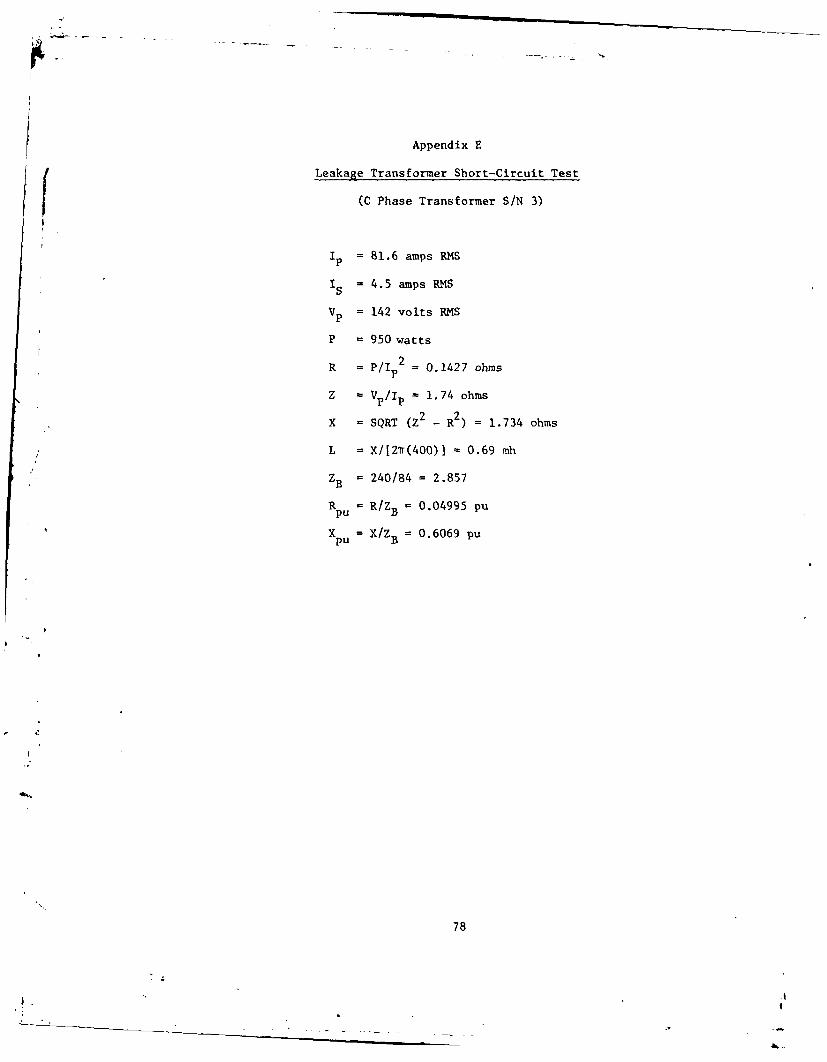
Appendix E
Leakage Transformer Short-Circuit Test
(C Phase Transformer S/N 3)
Ip = 81.6 amps RMS
i s = 4.5 amps RMS
VP = 142 volts RMS
P = 950 watts
R = P/I 2 - = 0.1427 ohms
Z = Vp/Ip = 1.74 ohms
X = SQRT (Z2 - R2) 1.734 ohms
L = X/121(400)] = 0.69 mh
ZB = 240/84 = 2.857
Rpu = R/ZB = 0.04995 pu
Xpu =X/Z = 0.6069 pu
78
,'I
Vita
William C. Dungan was born on July 24, 1946 in Lucedale, Mississippi.
He graduated from Rocky Creek High School, Lucedale, Mississippi in 1964
and attended Mississippi State University from which he received a Bach-
elor of Science degree in Electrical Engineering in 1970. He entered the
Air Force in July 1972 and was assigned to the Service Engineering Divi-
sion at the Warner Robins Air Logistics Center, Robins AFB, Georgia. His
reassignment to the Air Force Aero Propulsion Laboratory was made in
April 1977 where he served as a research and development engineer and as
a laboratory staff officer. He then entered the Air Force Institute of
Technology, School of Engineering, in June 1980.
Permanent Address: Route 8, Box 165
Lucedale, MS 39452
79
V~

UnclassifiedSECURITY CLASSIFICATION OF THIS PAGE (When Dita knieredJ
READ INSTRUCTIONSREPORT DOCUMENTAFION PAGE 13FFORF COMPLETING FORM
1. REPORT NUMER 2. GOVT ACCESSION NO. 3 RECIPIENT'S CATALOG NUMBER
AFIT/GE/EE/81D-18/_______________
4. TITLE (end Subtitle) 5 TYPE OF REPORT & PERIOD COVERED
AC RESONANT CHARGING FOR INTERFACING PRIME POWER 8S TR OAiRTO PULSE CONDITIONING CIRCUITS
6 PERFORMING OtO REPORT NUMBER
7. AUTHOR(s) 8 CONTRACT OR GRANT NUMBER(&)
William C. Dungan, Capt, JSAF
9. PERFORMING ORGANIZATION NAME AND ADDRESS 10 PROGRAM ELEMENT. PROJECT TASKSchool of Engineering AREA & WORK UNIT NUMBERS
Air Force Institute of Technology (AFIT)Wright-Patterson AFB, OH 45433
1. CONTROLLING OFFICE NAME AND ADDRESS 12 REPORT DATE
Electrical Equipment Division December 1981
DRDME-EAM 13, NUMBER OF PAGES
Ft. Belvoir, VA 22060 8614. MONITORING AGENCY NAME & ADDRESS(i( dilerent from Controlling Ofice) 1S. SECURITY CLASS. (of this report)
Unclassified
ISa. DECL ASSI FICATION DOWN GRADINGSCHEDULE
16. DISTRIBUTION STATEMENT (of tlA Report)
Approved for public release; distribution unlimited.
17. DISTRIBUTION STATEMENT (of the abstract entered in Block 20, if dlferent from Report)
18. SUPPLEMENTARY NOTES Dean-oReearchApproved for public release; lAWAFR 190-17,DeanoroReserch anProfessional Development
FR uEnIe C.. L friCr, "la-jo, USAF Air Force Institute of Technology (ATG)DifiCta of ,uhtT C ,,faTa ,' Wriht-Patterson AFB, OH 45433
19. KEY WORDS (Continue art reverse aide il necessary end identify by block number)
AC Resonant ChargingDC Resonant Charging
.* Pulse Power
20. ABSTRACT (Continue o n rvere side it necesery and identity by block number) The impact on a primepower source due to AC resonant charging was investigated. The source was a
standard DOD 15 KW, 400 Hz alternator. Adverse impact on the alternator was
almost negligible for a varying load of 15 to 60 KW and a frequency change of
380 to 475 Hz. The only exception was caused by the pulser diodes. Their
turn-on was reflected in the alternator voltage waveforms. An indirect approach
is presented for determining resonance and, thus, the internal reactance con-
tribution by the alternator. This value was found to be slightly less than
that specified for the leakage reactance. The investigation concludes that
DD AP73 1473 EDITION OF I NOV 65 IS OBSOLETE UnclassifiedSECURITY CLASSIFICATION OF THIS PAGE (%en Date Entered)
I.

unciassir ledSECURITY CLASSIFICATION OF THIS PAGE(Wh. Dale Fnt.,.d)
resonance, in the classical steady state sense, is never reached. Even thoughthe charging circuit has a transient response, the alternator armature greaction is approximately fixed. This implies that the alternator is in a nearsteady state mode of operation.
A
UnclassifiedSuURITY CLASSIFICATION OF 1'- PAOF(6h" Dea Et.Ierd$|

. .. .X . ....
3DAT
DTI