Embed Size (px)
Citation preview

232 IEEE TRANSACTIONS ON EDUCATION, VOL. 44, NO. 3, AUGUST 2001
Teaching MOS Integrated Circuit Amplifier Designto Undergraduates
David J. Comer, Senior Member, IEEE,and Donald T. Comer
Abstract—The enhancement-mode MOSFET is the primary ac-tive device used in present-day digital and mixed-signal integratedcircuit processes. Thus, it is important to introduce this deviceand associated circuit design methods early in the electronics cur-riculum. This article discusses four integrated circuit MOSFETamplifier configurations; the current source/active load stage, thesource follower, the cascode connection, and the differential stagewith a current mirror load. These stages serve as building blocksfor more complex MOSFET amplifiers and allow the introductionof MOSFET integrated circuit design principles.
Index Terms—Active load stage, cascode connection, MOSFETamplifier.
I. INTRODUCTION
E LECTRONIC circuit design had its genesis in the vacuumtube era and continued to evolve through the discrete
bipolar junction transistor era and through the BJT integratedcircuit (IC) era. It has now entered the MOSFET IC era. Mostanalog and mixed-signal circuit design today is done on aCMOS bulk process, using enhancement mode devices thathave very little relationship to their discrete MOSFET cousins.
The topic of analog electronic circuit design using MOSFETcircuits fabricated in CMOS processes is typically reserved fora senior or graduate elective course in most university curricula[1], using a textbook intended for a graduate audience [2]. It is,however, important to include basic material on MOSFET ICdesign in the initial electronic circuit design course to preparefor the advanced course. Even in curricula that have limited elec-tronic circuit design to a single required course, an appreciationfor the principles involved in IC design should be imparted tothe student.
Especially in programs that require only a single course, itis difficult to select topics that will be most important to thestudent. The need for completeness in electronics textbooks re-quires a breadth of coverage that makes it difficult to select themost appropriate material. The goal of this article is to suggestmaterial that, when incorporated into the first electronic circuitscourse, can provide a fundamental design background in theMOSFET IC amplifier design area. Generally, breadth of cov-erage will be sacrificed in the basic course to include a mean-ingful coverage of this popular area.
The first suggestion is to clearly delineate to the student thedifferences between discrete and IC MOSFET circuit design.
Manuscript received April 10, 2000; revised March 2, 2001.The authors are with the Department of Electrical and Computer En-
gineering, Brigham Young University, Provo, UT 84602 USA (e-mail:[email protected]).
Publisher Item Identifier S 0018-9359(01)06996-5.
These differences are covered in Section II. Next, some impor-tant building blocks that are currently important in the fabri-cation of MOSFET amplifiers are considered. A discussion ofthese building blocks allows design principles to be consideredand also demonstrates the necessity of simulation in MOSFETdesign. Section III includes four different building blocks thatmay be used in larger MOS amplifier circuits. The effects of asmall capacitive load and signal generator resistance on circuitperformance are demonstrated through Spice simulations.
The succeeding material assumes the readers’ familiaritywith the MOSFET device and its simple small-signal orincremental equivalent circuit.
II. DIFFERENCES BETWEENDISCRETE ANDINTEGRATED
CIRCUIT MOSFET DESIGN
One of the important differences between discrete and IC de-sign is in the components selected to minimize chip area [3].A resistor or capacitor typically occupies much more chip areathan a transistor. If one of these two passive elements can beeliminated by using additional transistors, the circuit cost will bedecreased. It is economical, for example, to replace load resis-tors found in discrete amplifiers with active loads, that is, otherMOSFET’s biased into the active region.
In addition, the ranges of values of both resistors and capac-itors are limited in IC design. The large chip areas required forthe fabrication of these elements in commonly used processesmight limit resistor values to 50 k and capacitor values to 50pF or less. The size and number of these passive elements arethen limited in order to conserve chip space. Large coupling ca-pacitors, used so freely in discrete amplifiers, are unavailable inIC amplifiers.
Because the numbers of resistors and capacitors are mini-mized in IC design, amplifier configurations that differ fromdiscrete configurations become more important. Of course, thedifferential stage [4], [5] is important, but so also are other lesscomplex stages that should be considered in the first electronicsclass.
In discrete devices, the substrate is generally tied to the sourceinside the package. Most CMOS processes require that sub-strates be tied to the appropriate rails, that is, the nMOS sub-strate is tied to the most negative rail and the pMOS substrate istied to the most positive. For those IC amplifier configurationshaving a source terminal that is not tied to a rail, the body effectmust be considered.
Another difference is in the consideration of channel widthin amplifier design. In MOSFET IC design, the selection ofchannel width is an integral part of the design procedure. This is
0018–9359/01$10.00 ©2001 IEEE

COMER AND COMER: TEACHING MOS INTEGRATED CIRCUIT AMPLIFIER DESIGN TO UNDERGRADUATES 233
not only different from MOSFET discrete design, but also dif-fers from bipolar junction transistor IC design. The transconduc-tance of a BJT depends on the dynamic base-emitter resistancewhich, in turn, depends on dc emitter current. It does not dependdirectly on dimensions. For a MOSFET, the channel width de-termines transconductance and is often critical to the design ofthe amplifier. For this reason, channel widths may vary from avalue near the minimum channel length up to a factor of hun-dreds or even thousands times this length.
Another difference in IC design relates to the increased diffi-culty in modeling modern small channel length devices and theincreased complexity of IC amplifiers. One result of this dif-ference is that most amplifier circuits are so complex that theycan be accurately analyzed only by simulation. Thus, simula-tion techniques become very important and should be integratedinto the first electronics class to prepare for succeeding classes.Spice-based programs are imperative to demonstrate the interac-tion of various parameters with overall amplifier performance.
III. MOSFET IC AMPLIFIER CONFIGURATIONS
Some useful amplifier configurations or building blocks are
1) the common-source stage with current source load (activeload stage),
2) the source-follower with current source load,3) the cascode stage, and4) the differential stage with current-mirror load.Since present classes typically cover the operation of the
simple current-mirror, a knowledge of this circuit is presumedbefore discussing the amplifier configurations mentioned.
A. Active Load Stage
A stage used often in IC design is the active load stage. Typ-ically, the active load is a current source, based on the currentmirror. The MOSFET active load stage might appear as in Fig. 1.
The pMOS current mirror provides bias current to the ampli-fying device, M1. This device sees a drain load that equals
(1)
The midband voltage gain is now
(2)
The output capacitance for the amplifier of Fig. 1 is
(3)
giving an upper corner frequency of
(4)
Of course, a load capacitance or input capacitance of a fol-lowing stage will lower this value. An example will demonstratethe use of these equations and the manner in which a simulationcan be related to the results.
Example: The current mirror of Fig. 1 supplies a current of50 A to the amplifying stage using values of k and
V. The dc output voltage is adjusted by voltage source,
Fig. 1. A MOSFET stage with an active current source load.
, to be 2.4 V. If mA V, A V,A V, fF, fF,
fF, and fF, calculate
a) the midband voltage gain, ;b) the upper corner frequency, ;c) verify results with a Spice simulation.Solution: The output resistance for this stage is
k
Using (2) leads to a voltage gain of
V V
The output capacitance is
fF
From (4), this gives an upper corner frequency of
MHz
The Spice simulation file is listed in Table I.This program uses a model for the MOSFETs named
C5X.LIB. The results of this simulation are V Vand MHz, which compare well with the calculatedresults.
In cascaded MOS stages, the load presented by the gate of afollowing stage is primarily capacitive. This is also the case foran output stage that connects to an IC pad and an output pin.Thus, it is important to see how a stage is affected when loadedwith capacitance. Furthermore, the output resistance of a stageserves as the generator resistance to the following stage. It isimportant to note how gain and upper corner frequency dependon the generator resistance in series with the input of the stage.

234 IEEE TRANSACTIONS ON EDUCATION, VOL. 44, NO. 3, AUGUST 2001
TABLE ISPICE FILE FOR EXAMPLE
The effect of a capacitive load or the effect of a generatorresistance on the upper corner frequency and the voltage gaincan be found by additional simulations.
The circuit of Fig. 1 is not driving a load. If this happens to bean output stage, its output will connect to an output pad of theIC chip. The capacitance associated with the pad might exceed1 pF. If the simulation is repeated with a 1 pF load added, theupper corner frequency drops from 8.35 MHz to 431 kHz.
If this stage were loaded by a comparable stage rather than by1 pF, the corner frequency might drop by a factor of two ratherthan a factor of 20. In order to avoid this drop, a buffer stagemay be added to drive the 1 pF load without the large reductionin corner frequency.
Another possibility is to increase the values of for all thedevices. While this increases the capacitance, the output resis-tance decreases and increases with to result in a compa-rable voltage gain. The effect of the load capacitance on uppercorner frequency will then be much less.
Another point relating to frequency response is that the sim-ulated circuit is driven by a perfect voltage source with zerooutput resistance. If this stage were driven by an identical stage,the output impedance of the first stage would become the sourceresistance for the second stage. To demonstrate the effect ofsource resistance on upper corner frequency, a resistance of 339k is used as a source resistance for the circuit of Fig. 1. Thisparticular value of resistance will be used in succeeding cir-cuit examples for comparison purposes. No external load ca-pacitance is used in this simulation. The simulated upper cornerfrequency is lowered in this situation from a value of 8.35 MHzto 3.08 MHz.
This value can also be calculated by noting that the inputcircuit will now cause a corner frequency determined by thesource resistance and the input capacitance. The input capaci-tance equals the sum of , , and the Miller effect capac-itance . From the simulation, these values are
V V fF
fF fF
The total input capacitance resulting is approximately 111 fF.With a 339 k source resistance, this adds a corner frequency
TABLE IIANALYSIS RESULTS FORACTIVE LOAD STAGE
of
MHz
The amplifier now has an input corner frequency of 4.23MHz and an output corner frequency of 8.53 MHz. An itera-tive method is used to calculate the overall upper corner fre-quency since two unequal single-poles determine the amplifierresponse. This results in a calculated overall corner frequencyof MHz. This value exceeds the simulatedvalue of 3.08 MHz by 15%.
If a source resistance of 339 kand a 1-pF load capacitanceare both added to the amplifier, the new upper corner frequencyis found from simulation to be 399 kHz.
Table II summarizes the results of this analysis.Generally, the capacitor values used in the manual calcula-
tions are found from the simulation that lists all parameter valuesat the bias point used.
This example demonstrates the use of an active load stage aswell as the degrading effects of a capacitive load and a signalgenerator resistance. These effects must be understood in orderto do effective IC design.
Approximate results are useful to provide a starting point forcircuitsimulationsthatareanecessitybeforeanICchip is laidout.Fabricationrunsareveryexpensive,andmistakesmustbeavoidedto minimize cost. Thus, the simulation step is never omitted in theICdesignprocess.Thisstepusesparameters for theMOSdevicesthat are based on the actual process to be used in fabrication.
B. Source Follower with Active Load
The source follower provides a buffer stage, but the midbandvoltage gain is low, even less than the value of unity approachedby the BJT emitter-follower stage. The bandwidth is quite highfor the source-follower stage. Fig. 2 demonstrates a source fol-lower with a current-mirror load.
ThedeviceM2presentsa resistanceof between thesourceof M1 and ground. In addition, device M1 presents a resistance of
in parallel with between the source of this device andthe dc power supply which is also ground for incremental signals.It should be noted that the body effect in M1 must be includedsince the source-to-substrate voltage of this device varies withthe output signal. In fact, it equals the output signal.
The circuit of Fig. 2(b) is redrawn in Fig. 3 and the pertinentparasitic capacitances are added.
The two current sources and can be con-verted to conductances and , respectively. Fig. 4 showsan alternate equivalent circuit that is used to find the voltagegain as a function of frequency.

COMER AND COMER: TEACHING MOS INTEGRATED CIRCUIT AMPLIFIER DESIGN TO UNDERGRADUATES 235
Fig. 2. (a) A source-follower stage with current source load. (b) Equivalent circuit.
Fig. 3. The high-frequency source-follower equivalent circuit.
Fig. 4. Alternate equivalent circuit of the source follower.
The circuit of Fig. 4 is analyzed to find that
(5)
where
(6)
and
(7)
The midband gain can be evaluated by combining (5) and (6)and is
(8)
In many submicron processes, the value of the denominator of(8) might equal 1.15 to 1.2 times . This leads to values ofmidband gain ranging from about 0.8 to 0.9 V/V.
The transfer function for voltage gain as a function of fre-quency shows a zero at
(9)
and a pole at
(10)
Typically, the zero frequency is higher than the pole fre-quency and the asymptotic frequency response appears as inFig. 5.
At high frequencies the capacitor feeds through frominput directly to output causing a gain of
(11)
In simulating a source-follower circuit with similar dimen-sions to those of the devices in the earlier example, the midbandgain was found to be 0.81 V/V, and the upper corner frequencywas 1.15 GHz. This was for a circuit with no input signal sourceresistance and no load capacitance. With a signal source resis-tance of 339 k and a 1-pF load capacitance, the upper cornerfrequency becomes 37 MHz. This value is much higher than thatof the common-source, active-load stage.
Useful principles to be stressed from the source-follower cir-cuit are 1) the degrading effect on voltage gain of the nonzerovoltage appearing at the source of the MOSFET and 2) the ex-cellent frequency response of the circuit even in the presence oflarge capacitive loads.
As noted earlier, capacitive loading can be a serious problemfor an output stage that connects to an IC pin which will con-nect to the input of another circuit. Because of the high outputresistance of configurations such as the active load stage, a smallcapacitance of a pF or less will decrease the upper corner fre-quency significantly. The source follower stage is often insertedbetween a high-gain stage and the output pin of a chip to serveas a buffer stage. This buffer presents a rather low capacitanceto the preceding stage since there is no Miller multiplication of
and, as seen from the simulation, a 1 pF load capacitancecan result in a reasonably high upper corner frequency.
236 IEEE TRANSACTIONS ON EDUCATION, VOL. 44, NO. 3, AUGUST 2001
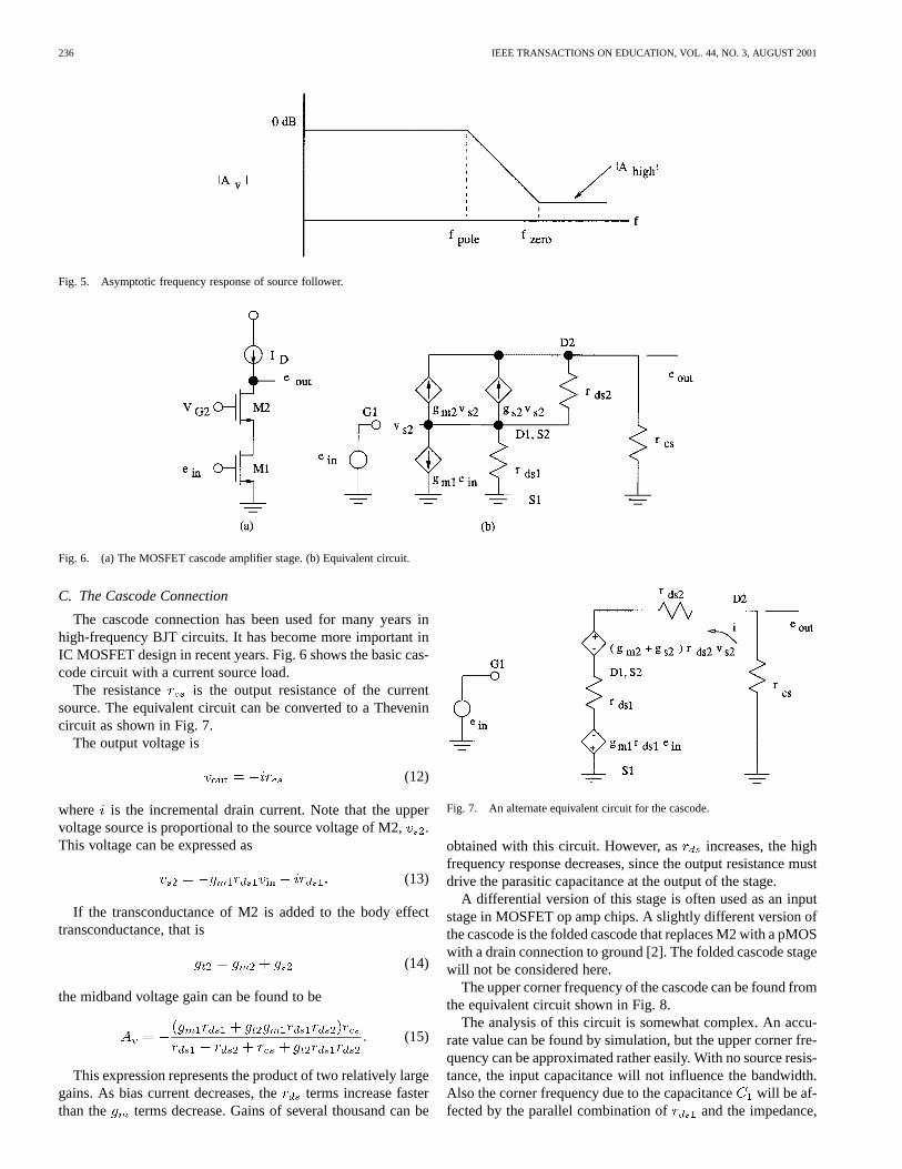
Fig. 5. Asymptotic frequency response of source follower.
Fig. 6. (a) The MOSFET cascode amplifier stage. (b) Equivalent circuit.
C. The Cascode Connection
The cascode connection has been used for many years inhigh-frequency BJT circuits. It has become more important inIC MOSFET design in recent years. Fig. 6 shows the basic cas-code circuit with a current source load.
The resistance is the output resistance of the currentsource. The equivalent circuit can be converted to a Thevenincircuit as shown in Fig. 7.
The output voltage is
(12)
where is the incremental drain current. Note that the uppervoltage source is proportional to the source voltage of M2,.This voltage can be expressed as
(13)
If the transconductance of M2 is added to the body effecttransconductance, that is
(14)
the midband voltage gain can be found to be
(15)
This expression represents the product of two relatively largegains. As bias current decreases, the terms increase fasterthan the terms decrease. Gains of several thousand can be
Fig. 7. An alternate equivalent circuit for the cascode.
obtained with this circuit. However, as increases, the highfrequency response decreases, since the output resistance mustdrive the parasitic capacitance at the output of the stage.
A differential version of this stage is often used as an inputstage in MOSFET op amp chips. A slightly different version ofthe cascode is the folded cascode that replaces M2 with a pMOSwith a drain connection to ground [2]. The folded cascode stagewill not be considered here.
The upper corner frequency of the cascode can be found fromthe equivalent circuit shown in Fig. 8.
The analysis of this circuit is somewhat complex. An accu-rate value can be found by simulation, but the upper corner fre-quency can be approximated rather easily. With no source resis-tance, the input capacitance will not influence the bandwidth.Also the corner frequency due to the capacitancewill be af-fected by the parallel combination of and the impedance,

COMER AND COMER: TEACHING MOS INTEGRATED CIRCUIT AMPLIFIER DESIGN TO UNDERGRADUATES 237
Fig. 8. High-frequency model of the cascode.
, looking into the source of M2. This impedance will bemuch less than and can be approximated by
(16)
This corner frequency will be quite large, at least comparedto that caused by . The resistance seen by this capacitanceis where is the output impedance of a simplecurrent mirror, and is the impedance looking into the drainof M2. This latter impedance will be quite large since the sourceresistance of M2 equals . This output resistance of M2 willbe very high; thus, the resistance seen byis approximately
. The upper corner frequency of the cascode can then beapproximated by
(17)
where .A simulation with all dc drain currents at 50A results in
V/V and MHz. In order to demon-strate the effect of current on gain and bandwidth, the circuit issimulated for a drain current of 10.7A. For this situation, thesimulated results are V/V and MHz.The gain has approximately doubled while the bandwidth hasdropped by a factor of about 4.
If a source resistance is present, a second corner frequency isadded at the input due to of Fig. 8. When a 339 k sourceresistance is added to the cascode circuit with A, thenew upper corner frequency is 8.95 MHz, representing a rela-tively small change from the original value of 9.65 MHz. Thisresult implies that is rather small. It should be emphasizedfor the cascode connection that the input capacitance is smallsince the Miller effect is minimized by a small voltage gain fromgate to drain of M1.
If a load capacitance of 1 pF is added, but no source resistanceis present, the upper corner frequency is lowered to 552 kHz.Adding the source resistance to this circuit leads to no furtherreduction of the upper corner frequency.
D. The Differential Connection with Current Mirror Load
This stage is significant in that it preserves the goodcommon-mode rejection properties of the double-ended outputdifferential stage, but produces a single-ended output signal.Fig. 9 shows a block diagram of such an arrangement.
With no input signal applied to the differential stage, the tailcurrent splits equally between and . The input currentto the mirror then equals . This value is also mirrored to
Fig. 9. Differential pair with current mirror load.
the output of the mirror giving . It is assumed thatthe voltage between the current mirror output and the seconddifferential stage is approximately zero, although this assump-tion is unnecessary to achieve the correct result.
When a signal is applied to the differential input, it may in-crease the current by a peak value of . The input currentto the mirror now becomes
(18)
The output current from the mirror also equals this value.However, the input signal to the differential stage will decrease
by the same amount that increases. Thus, we canwrite
(19)
The current to the resistanceincreases from its quiescentvalue of zero to
(20)
The incremental output voltage resulting is then
(21)
When an incremental input signal is applied to the differentialpair, half of this voltage will drop across each gate-source ter-minal pair. The gate-source voltages result in equal incrementaldifferential stage currents in the two output devices, but these

238 IEEE TRANSACTIONS ON EDUCATION, VOL. 44, NO. 3, AUGUST 2001
currents will be in opposite directions. An incremental inputsignal, , will produce incremental currents of
(22)
and
(23)
where is the transconductance of devices 1 and 2.Assuming negligibly large output resistances of the current
mirror and the differential stage, the incremental output voltagebecomes
(24)
with a resulting gain of
(25)
If the output resistances of the mirror and differential stageare significant, they can be combined in parallel with the loadresistance to use in (25). The load resistance may, in fact, be thesmall-signal input resistance of the following stage. Very largevalues of voltage gain can result from this configuration.
While this expression is the same as that for the differentialgain of a resistive load stage, two significant points should bemade. First of all, the impedance can be much greater thanany resistive load that can be used in a differential stage. Largevalues of in the differential stage would cause saturation of thestages for reasonable values of tail current. The current mirrorsolves this problem. The second point is that the output voltageof the differential pair with a current mirror load is a single-ended output which can be applied to a following simple am-plifier stage. However, the rejection of common-mode variablescaused by such factors as temperature change is still in effectwith the current mirror stage. If a resistive load stage must pro-vide a single-ended output, the gain drops by a factor of 2 andcommon-mode rejection no longer takes place.
IV. CONCLUSION
This article suggests a means of teaching MOSFET IC designin the first electronic circuit design course. The proposed circuitconfigurations represent several useful single-stage amplifiersencountered in IC design. A consideration of these amplifierbuilding blocks can serve as the vehicle to convey principles of
IC circuit design and prepare students for more advanced circuitdesign courses.
The importance of simulation in circuit design can be demon-strated by simulating the operation of several of the buildingblock circuits. Modifications in loading of the input and outputcircuits emphasize the utility of simulation programs.
REFERENCES
[1] D. T. Comer, “Putting mixed-signal technology into the curriculum,” inProc. Frontiers Educ. Conf., Washington, DC, Nov. 1993, pp. 426–428.
[2] D. A. Johns and K. Martin,Analog Integrated Circuit Design. NewYork: Wiley, 1997.
[3] P. R. Gray and R. G. Meyer,Analysis of Analog Integrated Circuits, 3rded. New York: Wiley, 1993.
[4] M. H. Rashid, Microelectronics Circuits: Analysis and De-sign. Boston, MA: PWS, 1999.
[5] A. S. Sedra and K. C. Smith,Microelectronic Circuits, 4th ed. NewYork: Oxford Univ. Press, 1998.
David J. Comer (M’64–SM’69) received the B.S., M.S., and Ph.D. degreesfrom San Jose State University, San Jose, CA, the University of California, andWashington State University, Pullman, respectively, all in electrical engineering.
From 1959 to 1964, he was employed by the IBM Corporation, who patentedthree of his circuit developments. In 1964, he became an Assistant Professorat the University of Idaho. He moved to the University of Calgary as an Asso-ciate Professor in 1966. In 1969, he became Professor and Chairman, Divisionof Engineering, California State University, Chico, where he received the Pro-fessional Achievement Award in 1981. He has authored ten textbooks and morethan 50 articles in the fields of communication circuits, circuit synthesis, com-puter-aided circuit design, and digital system design. He assumed his presentposition as Professor of Electrical and Computer Engineering at Brigham YoungUniversity, Provo, UT, in 1981.
Dr. Comer has been selected as the Outstanding ECE Professor and as theOutstanding Professor in Engineering and Technology. He received the awardfor Outstanding EE Professor from the University of Calgary in 1968.
Donald T. Comer received the B.S., M.S., and Ph.D. degrees from San JoseState University, San Jose, CA, the University of California, and the Universityof Santa Clara, Santa Clara, CA, respectively, all in electrical engineering.
He began teaching at San Jose State University in 1961 and combinedteaching and industrial work until he left San Jose State University in 1979.He has worked for California Technical Industries, IBM Corporation, MobilitySystems, Precision Monolithics, Storage Technology Corporation, and AnalogDevices during his career. In addition, he has served as consultant to suchfirms as Fairchild, Siemens, Zilog, and Micropower Systems. He is presentlya Professor of Electrical and Computer Engineering at Brigham YoungUniversity, Provo, UT, and a consultant to American Microsystems, Inc. Heholds 15 patents and has published more than 50 articles dealing with solidstate and integrated circuits. He has published three textbooks in the fields oflarge-signal and integrated circuits.
Dr. Comer formerly held the Quentin Berg Chair at the Pennsylvania StateUniversity, Harrisburg, and the Endowed Chair of Engineering at BrighamYoung University.