Embed Size (px)
Citation preview

APPLICATION NOTE
TEA2260/TEA2261HIGH PERFORMANCE DRIVER CIRCUITS FOR S.M.P.S
AN376/0694
SUMMARY Page
I INTRODUCTION. . . . . . . . . . . . . . . . . . . . . . . . . . . . . . . . . . . . . . . . . . . . . . . . . . . . . . . 2
I.1 MASTER SLAVE MODE. . . . . . . . . . . . . . . . . . . . . . . . . . . . . . . . . . . . . . . . . . . . . . . . . 2I.2 BURST MODE . . . . . . . . . . . . . . . . . . . . . . . . . . . . . . . . . . . . . . . . . . . . . . . . . . . . . . . . 2I.3 OPERATION OF MASTER SLAVE POWER SUPPLY IN TV APPLICATION . . . . . . . . 2I.4 SECONDARY REGULATION . . . . . . . . . . . . . . . . . . . . . . . . . . . . . . . . . . . . . . . . . . . . . 6I.5 PRIMARY REGULATION . . . . . . . . . . . . . . . . . . . . . . . . . . . . . . . . . . . . . . . . . . . . . . . . 8
II CIRCUIT DESCRIPTION . . . . . . . . . . . . . . . . . . . . . . . . . . . . . . . . . . . . . . . . . . . . . . . . 9
II.1 VOLTAGE REFERENCE AND INTERNAL VCC GENERATION. . . . . . . . . . . . . . . . . . . 10II.2 OSCILLATOR . . . . . . . . . . . . . . . . . . . . . . . . . . . . . . . . . . . . . . . . . . . . . . . . . . . . . . . . . 10II.3 ERROR AMPLIFIER . . . . . . . . . . . . . . . . . . . . . . . . . . . . . . . . . . . . . . . . . . . . . . . . . . . . 12II.4 PULSE WIDTH MODULATOR . . . . . . . . . . . . . . . . . . . . . . . . . . . . . . . . . . . . . . . . . . . . 12II.5 SOFT START OPERATION . . . . . . . . . . . . . . . . . . . . . . . . . . . . . . . . . . . . . . . . . . . . . . 13II.6 BURST GENERATION IN STAND BY . . . . . . . . . . . . . . . . . . . . . . . . . . . . . . . . . . . . . . 13II.7 IS LOGIC. . . . . . . . . . . . . . . . . . . . . . . . . . . . . . . . . . . . . . . . . . . . . . . . . . . . . . . . . . . . . 14
II.8 SAFETY FUNCTIONS : DIFFERENCES BETWEEN TEA2260 AND TEA2261. . . . . . . 15II.8.1 I max . . . . . . . . . . . . . . . . . . . . . . . . . . . . . . . . . . . . . . . . . . . . . . . . . . . . . . . . . . . . . . . . 16II.8.1.1. First threshold VIM1 . . . . . . . . . . . . . . . . . . . . . . . . . . . . . . . . . . . . . . . . . . . . . . . . . . 17II.8.1.2. Second threshold VIM2 for TEA2260 . . . . . . . . . . . . . . . . . . . . . . . . . . . . . . . . . . . . . 18II.8.1.3. Second threshold VIM2 for TEA2261 . . . . . . . . . . . . . . . . . . . . . . . . . . . . . . . . . . . . . 18II.8.2 Logical block . . . . . . . . . . . . . . . . . . . . . . . . . . . . . . . . . . . . . . . . . . . . . . . . . . . . . . . . . . 18II.8.2.1. Logical block for TEA2260 . . . . . . . . . . . . . . . . . . . . . . . . . . . . . . . . . . . . . . . . . . . . . 18II.8.2.2. Logical block for TEA2261 . . . . . . . . . . . . . . . . . . . . . . . . . . . . . . . . . . . . . . . . . . . . . 19II.9 OUTPUT STAGE . . . . . . . . . . . . . . . . . . . . . . . . . . . . . . . . . . . . . . . . . . . . . . . . . . . . . . 19
III TV APPLICATION 120W 22O VAC 16KHz SYNCHRONIZED . . . . . . . . . . . . . . . . . . . 20
III.1 CHARACTERISTICS OF APPLICATION . . . . . . . . . . . . . . . . . . . . . . . . . . . . . . . . . . . . 20
III.2 CALCULATION OF EXTERNAL COMPONENTS . . . . . . . . . . . . . . . . . . . . . . . . . . . . . 20III.2.1 Transformer calculation. . . . . . . . . . . . . . . . . . . . . . . . . . . . . . . . . . . . . . . . . . . . . . . . . . 21III.2.1.1 Transformer specification . . . . . . . . . . . . . . . . . . . . . . . . . . . . . . . . . . . . . . . . . . . . . . 22III.2.2 Switching transistor and its base drive . . . . . . . . . . . . . . . . . . . . . . . . . . . . . . . . . . . . . . 22III.2.2.1 Current limit calculation . . . . . . . . . . . . . . . . . . . . . . . . . . . . . . . . . . . . . . . . . . . . . . . . 22III.2.2.2 Snubber network . . . . . . . . . . . . . . . . . . . . . . . . . . . . . . . . . . . . . . . . . . . . . . . . . . . . . 23III.2.2.3 Base drive . . . . . . . . . . . . . . . . . . . . . . . . . . . . . . . . . . . . . . . . . . . . . . . . . . . . . . . . . . 24III.2.3 Oscillator frequency . . . . . . . . . . . . . . . . . . . . . . . . . . . . . . . . . . . . . . . . . . . . . . . . . . . . 25III.2.4 Regulation loop . . . . . . . . . . . . . . . . . . . . . . . . . . . . . . . . . . . . . . . . . . . . . . . . . . . . . . . . 25III.2.5 Overload capacitor . . . . . . . . . . . . . . . . . . . . . . . . . . . . . . . . . . . . . . . . . . . . . . . . . . . . . 26III.2.6 Soft start capacitor . . . . . . . . . . . . . . . . . . . . . . . . . . . . . . . . . . . . . . . . . . . . . . . . . . . . . 26III.2.7 Feedback voltage transformer . . . . . . . . . . . . . . . . . . . . . . . . . . . . . . . . . . . . . . . . . . . . 26III.2.8 Start up resistor. . . . . . . . . . . . . . . . . . . . . . . . . . . . . . . . . . . . . . . . . . . . . . . . . . . . . . . . 27III.2.9 High voltage filtering capacitor . . . . . . . . . . . . . . . . . . . . . . . . . . . . . . . . . . . . . . . . . . . . 28III.3 ELECTRICAL DIAGRAM . . . . . . . . . . . . . . . . . . . . . . . . . . . . . . . . . . . . . . . . . . . . . . . . 29
1/33

SUMMARY (continued) Page
IV TV APPLICATION 140W 220 VAC 32kHz SYNCHRONIZED . . . . . . . . . . . . . . . . . . . . 32
IV.1 APPLICATION CHARACTERISTICS . . . . . . . . . . . . . . . . . . . . . . . . . . . . . . . . . . . . . . . 32
IV.2 TRANSFORMER CHARACTERISTICS . . . . . . . . . . . . . . . . . . . . . . . . . . . . . . . . . . . . . 32
IV.3 ELECTRICAL DIAGRAM . . . . . . . . . . . . . . . . . . . . . . . . . . . . . . . . . . . . . . . . . . . . . . . . 33
V TV APPLICATION 110W 220 VAC 40kHz REGULATED BY OPTOCOUPLER . . . . . . 34
V.1 FREQUENCY SOFT START . . . . . . . . . . . . . . . . . . . . . . . . . . . . . . . . . . . . . . . . . . . . . 34
V.2 APPLICATION CHARACTERISTICS . . . . . . . . . . . . . . . . . . . . . . . . . . . . . . . . . . . . . . . 34
V.3 TRANSFORMER SPECIFICATION . . . . . . . . . . . . . . . . . . . . . . . . . . . . . . . . . . . . . . . . 34
V.4 ELECTRICAL DIAGRAM . . . . . . . . . . . . . . . . . . . . . . . . . . . . . . . . . . . . . . . . . . . . . . . . 35
I - INTRODUCTIONThe TEA2260/61 is an integrated circuit able todrive a bipolar transistor directly with an outputbase current up to 1.2A.So the TEA 2260/61 covers a wide range of appli-cation from 80W to more than 200W with all safetyrequirements respected.The high performances of the regulation loop pro-vide a very low output power due to an automaticburst mode.The TEA2260/61 can be used in a MASTERSLAVE STRUCTURE, in a PRIMARY REGULA-TION or a SECONDARY REGULATION.The TEA 2260/61 is very flexible and high perform-ance device with a very large applications field.The only difference between TEA2260 andTEA2261 concerns security functions (see para-graph II.8)
I.1 - Master Slave Mode (Figure 1)In this configuration the master circuit located onthe secondary side, generates PWM pulses usedfor output voltage regulation. These pulses are sentvia a feedback transformer to the slave circuit(Figure 1).In this mode of operation, the falling edge of thePWM Signal may be synchronized with an externalsignal. By this way the switching off time of thepower transistor, which generates lot of parasites,can be synchronized on the line flyback signal inTV applications.An other advantage of the MASTER SLAVESTRUCTURE is to have a very good regulation notdepending of the coupling between transformerprimary and secondary windings, which allows theuse of low cost switch mode transformers.
I.2 - Burst Mode (Figure 2)During start-up and stand-by phases, no regulationpulses are provided by the master circuit to theslave circuit.The slave circuit operates in primary regulationmode. When the output power is very low the burstmode is automatically used.This operating mode of the SMPS effectively pro-vides a very low output power with a high efficiency.The TEA2260/61 generates bursts with a periodvarying as a function of the output power.Thus the output power in burst mode can varied ina wide range from 1W to more than 30W.
I.3 - Operation of Master Slave Power Supplyin TV ApplicationThe system architecture generally employed is de-picted in Figure 3. On the secondary side a microcontroller is connected to the remote control re-ceiver which generates control signal for the stand-by and normal modes of operation (Figure 4).- In stand-by mode, the device power consumption
is very low (few watts). The master circuit doesnot send pulses and hence the slave circuit worksin primary regulation and burst mode.
- In the normal mode, the master circuit providesthe PWM signal required for regulation purposes.This is called MASTER SLAVE MODE. The mas-ter circuit can be simultaneously synchronizedwith the line flyback signal.
- Power supply start-up. As soon as the VCC(start)threshold is reached, the slave circuit starts incontinuous mode and primary regulation as longas the nominal output voltages are not reached.After this start-up phase the microcontroller holdsthe TV Set in stand-by mode or either in normalmode.
HIGH PERFORMANCE DRIVER CIRCUITS FOR S.M.P.S
2/33

SLAVECIRCUIT
MASTERCIRCUIT
Sync.Pulses
PulseInput
BaseCurrent
PWMSignal
376-
01.E
PS
Figure 1
Burst Periodtyp 30ms~~
COLLECTOR CURRENT ENVELOP DETAIL OF ONE BURST
SwitchingPeriod
376-
02.E
PS
Figure 2 : Burst Mode Operation
HIGH PERFORMANCE DRIVER CIRCUITS FOR S.M.P.S
3/33

AU
DIO
OU
TP
UT
ST
AG
E
SC
AN
NIN
GD
EV
ICE
TE
A51
70
MA
INS
INP
UT
R C
TEA
2260
/61
VO
LTA
GE
RE
GU
LAT
OR
µ P
INF
RA
-RE
DR
EC
EIV
ER
Mut
ing
Con
trol
Rem
ote
Sta
nd-b
y
Rem
ote
Sta
nd-b
y
Syn
chro
niza
tion
VC
C
2P
P1
VC
C
21P
: O
utpu
t vol
tage
adj
uste
men
t in
norm
al m
ode
P
: Out
put v
olta
ge a
djus
tem
ent i
n st
and-
by
Sm
all s
igna
l prim
ary
grou
ndP
ower
prim
ary
grou
ndS
econ
dary
gro
und
(isol
ated
from
mai
ns)
PW
M
376-
03.E
PS
Figure 3 : TV Application System Diagram
HIGH PERFORMANCE DRIVER CIRCUITS FOR S.M.P.S
4/33

Sta
rt-u
pS
tand
-by
Nor
mal
ope
ratio
nS
tand
-by
t t t t tt 1
1
2S
tand
-by
cont
rol
volta
ge
µ P s
uppl
yvo
ltage
2
1
TE
A51
70O
utpu
t vol
tage
enve
lop
Out
put
volta
ge
Col
lect
orcu
rren
ten
velo
p
V
V
CC
CC
(ST
AR
T) CC
(ST
OP
)
12
t 2
TE
A22
60/6
1V
volta
ge
* t
and
t
: co
mm
ands
issu
ed b
y µ P
376-
04.E
PS
Figure 4 : System Description (waveforms)
HIGH PERFORMANCE DRIVER CIRCUITS FOR S.M.P.S
5/33

I.4 - Secondary Regulation (Figures 5 and 6)
In this configuration the TEA2260/61 provides theregulation through an optocoupler to ensure goodaccuracy.
The advantage of this configuration is the avaibilityof a large range of output power variation (e.g 1Wto 110W).
This feature is due to the automatic burst mode(see paragraph II.6).
The structure in a TV Set is simpler than theMASTER SLAVE STRUCTURE because thepower supply switches from normal mode to burstmode automatically as a function of the outputpower.
AU
DIO
OU
TP
UT
ST
AG
E
SC
AN
NIN
GD
EV
ICE
MA
INS
INP
UT
R C
TEA
2260
/61
VO
LTA
GE
RE
GU
LAT
OR
µ P
INF
RA
-RE
DR
EC
EIV
ER
Mut
ing
Con
trol
Rem
ote
Sta
nd-b
y
VC
C
P
VC
C
P :
Out
put v
olta
ge a
djus
tem
ent
Sm
all s
igna
l prim
ary
grou
ndP
ower
prim
ary
grou
ndS
econ
dary
gro
und
(isol
ated
from
mai
ns)
376-
05.E
PS
Figure 5 : TV Application System Diagram
HIGH PERFORMANCE DRIVER CIRCUITS FOR S.M.P.S
6/33

Sta
rt-u
pS
tand
-by
Nor
mal
ope
ratio
nS
tand
-by
t t t t tt 1
1µ P
sup
ply
volta
ge
Out
put
volta
ge
Col
lect
orcu
rren
ten
velo
p
V
V
CC
CC
(ST
AR
T) CC
(ST
OP
)
12
t 2
TE
A22
60/6
1V
volta
ge
* t
and
t
: co
mm
ands
issu
ed b
y µ P
Sta
nd-b
yvo
ltage
enve
lop
376-
06.E
PS
Figure 6 : System Description (waveforms)
HIGH PERFORMANCE DRIVER CIRCUITS FOR S.M.P.S
7/33

I.5 - Primary Regulation (Figure 7)
In this configuration the TEA2260/61 provides theregulation through an auxilliary winding.
This structure is very simple but the accuracy de-
pends on the coupling between the transformerprimary and secondary winding.
Due to the automatic burst mode the output powercan vary in a large range.
AU
DIO
OU
TP
UT
ST
AG
E
SC
AN
NIN
GD
EV
ICE
MA
INS
INP
UT
R C
TEA
2260
/61
VO
LTA
GE
RE
GU
LAT
OR
µ P
INF
RA
-RE
DR
EC
EIV
ER
Mut
ing
Con
trol
Rem
ote
Sta
nd-b
y
VC
C
P
VC
C
P :
Out
put v
olta
ge a
djus
tem
ent
Sm
all s
igna
l prim
ary
grou
ndP
ower
prim
ary
grou
nd
Sec
onda
ry g
roun
d (is
olat
ed fr
om m
ains
)
376-
07.E
PS
Figure 7 : TV Application System Diagram
HIGH PERFORMANCE DRIVER CIRCUITS FOR S.M.P.S
8/33

II - CIRCUIT DESCRIPTION
Figure 8 shows the integrated functions.
7
6
1615
14
38
21
1011
94
512
13
ER
RO
R A
MP
LIF
LIE
R
INT
ER
NA
LB
IAS
MO
DU
LAT
OR
LOG
IC
AU
TO
MA
TIC
BU
RS
TG
EN
ER
AT
ION
ISLO
GIC
LOG
ICP
RO
CE
SS
OR
V
MO
NIT
OR
ING
CC
RE
FV
(2.4
9V)
PO
SIT
IVE
OU
TP
UT
ST
AG
E
NE
GA
TIV
EO
UT
PU
TS
TA
GE
RE
PE
TIT
IVE
OV
ER
LOA
DP
RO
TE
CT
ION
CU
RR
EN
TLI
MIT
AT
ION
SE
CO
ND
AR
YP
ULS
E
0.15
V0.
6V2.
55V
0.9V
10µ A
45µ A
PR
IMA
RY
PU
LSE
SR
EG
ULA
TIO
NP
ULS
ES
OV
ER
VO
LTA
GE
PR
OT
EC
TIO
N
15.7
V
DE
MA
GN
ET
IZA
TIO
NS
EN
SIN
G
MO
DU
LAT
OR
S
V 2.49
VR
EF
7.4V
10.3
V
OS
CIL
LAT
OR
ON
(Max
.)
CC
V
+ 1.
2A(M
ax.)
E
SV
V +
CC
OU
T
GN
DI M
AX
C2
INIS
CC
10
0R
+- +- + -
+
-
+
-
+-
+
-
+
-T
(60
%)
SO
FT
-STA
RT
- 1
- 2A
(Max
.)
376-
08.E
PS
Figure 8
HIGH PERFORMANCE DRIVER CIRCUITS FOR S.M.P.S
9/33

The circuit contains 8 blocks :- Voltage reference and internal VCC generation.- RC oscillator- Error amplifier- Pulse width modulator (PWM)- "Is logic" for transformer demagnetization check-
ing.- Current limitation sub-unit (IMAX)- Logical block.- Output stage.
II.1 - Voltage Reference and Internal V CC Gen-eration (Figure 9)This block generates a 2.5V typ. voltage reference
valid as soon as VCC exceeds 4V. It is not directlyaccessible externally but is transmitted to otherblocks of the circuit.
This block also generates an internal regulatedVCC, VCC(int), the nominal value of which is 5V.VCC(int) supplies the circuit when Vcc is higher thanVCC(start) (10.3V typ.). This allows the circuit to achieve a good externalVCC rejection, and to provide high performanceeven with large VCC supply voltage variations.This block also generates initialization and controlsignals for the logical block. It also contains theVCC(Max.) comparator (typ threshold 15.7V).
II.2 - Oscillator (Figures 10 and 11)The oscillator determines the switching frequencyin primary regulation mode. Two external compo-nents are required : a resistor RO and a capacitorCO. The oscillator generates a sawtooth signal,which is available on Pin 10.
376-
09.E
PS
Figure 9 : Voltage Reference Block Principle
376-
10.E
PS
Figure 10 : Operating Principle
HIGH PERFORMANCE DRIVER CIRCUITS FOR S.M.P.S
10/33
CO capacitor is charged with a constant current.The current is fixed by RO which is supplied byvoltage VREF.
Ich = 2.5RO
When the vo ltage across CO reaches23
x VCCint (typ 3.33V), Q Transistor conducts and
CO is quickly discharged into an 2kΩ (typ) internalres istor. When the vo ltage reaches
1/3 x VCCint (typ 1.66V), the discharge is stopped,and the linear charge starts again.Theoretical values of T,T1 and T2 as function of ROand CO :
T = CO (0.69 x RO + 1380)T1 = RO x CO x 0.69T2 = CO x 2000 x 0.69 = CO x 1380
Due to the time response of comparators andnormal spread on thresholds values, the real val-ues of T1 and T2 may be slightly different, comparedwith these theoretical values (see Figure 12).
376-
11.E
PS
Figure 11 : Sawtooth available accross CO
376-
12.E
PS
Figure 12 : Frequency as a Function of RO and CO
HIGH PERFORMANCE DRIVER CIRCUITS FOR S.M.P.S
11/33

376-
14A
.EP
S /
376-
14B
.EP
S
Figure 14
II.3 - Error Amplifier (Figure 13)
It is made of an operational amplifier. The open loopgain is typically 75dB. The unity gain frequency is550kHz (typ). An internal protection limits the out-put current (Pin 7) at 2mA in case of shorted toground.
376-
13.E
PS
Figure 13
Output and inverting input are accessible thusgiving high flexibility in use. The non-inverting inputis not accessible and is internally connected toVREF (or 0.9VREF in burst mode - see paragraph II.6)
Before driving the pulse width modulator (PWM)and in order to get the appropriate phase, the erroramplifier is followed by an inverter.
II.4 - Pulse Width Modulator (PWM) (Figure 14)
The pulse width modulator consists of a compara-tor fed by the output signal of the error amplifier andthe oscillator output. Its output is used to generateconduction signal.
The TEA2260/61 actually integrates two PWM :
- A main PWM generates a regulation signal (∝) bycomparing the error signal (inverted) and thesawtooth.
- An auxiliary PWM generates a maximum dutycycle conduction signal (β), by comparing thesawtooth with an internal fixed voltage. Further-more, during the starting phase of the SMPS, inassociation with an external capacitor, this PWMgenerates increasing duty cycle, thus allowing a"soft" start-up.
- A logic "AND" between signals (∝) and (β) pro-vides the primary regulator output signal TA.
HIGH PERFORMANCE DRIVER CIRCUITS FOR S.M.P.S
12/33

376-
16.E
PS
Figure 16 : C1 Voltage (Pin 9)
376-
15.E
PS
Figure 15
II.5 - Soft Start Operation (Figure 16)From t1 to t2, there is no output pulse (pin 14) andC1 is charged by a 180µA current (typically). WhenC1 voltage reaches 1.5V (typically), output pulsesappear and the charge current of C1 is divided by20 (9µA typically), then the duty cycle increasesprogressively. When C1 voltage reaches 2.7V (typi-cally), the soft-starting device ceases to limit theduty cycle, which may reach 60%.Under established conditions C1 voltage is chargedto 3.1V (typically)
II.6 - Burst Generation in Stand By (primaryregulation mode)
When the SMPS output power becomes very low,the duty cycle of the switching transistor conductionbecomes also very low. In order to transmit a lowaverage power, while ensuring correct switchingconditions to the power transistor, a "burst" systemis used for energy transmission in stand by mode.
PrincipleFor a medium output power (e.g. more than 10W),
the voltage reference is applied to the non- invert-ing input of the error amplifier. When output powerdecreases as the minimum conducting time of thepower transistor is reached, the output voltagetends to increase. Consequently the error signalapplied to the PWM becomes higher than the saw-tooth. This is detected by a special logic and thevoltage applied to the non inverting input becomesVREF = 0.9 x 2.5 = 2.25V typically.
Consequently the regulation loop is in an overvol-tage equivalent state and the output pulses disap-pear. The output voltage decreases and when itreaches a value near 0.9 times the normal regula-tion value , the voltage applied to the non invertinginput is switched again to the normal valueVREF = 2.5V. Pulses applied to the power transistorreappear, the output voltage increases again, andso on... A relaxation operation is obtained, gener-ating the burst.
Futhermore, to avoid a current peak at the begin-ning of each burst, the soft-start is used at thisinstant.
Advantages of this method
- improved power supply efficiency compared withtraditional systems, for low power transmission.
- automatic burst-mode continuous mode transi-tion, as a function of the output power.
- high stand-by power range.- burst frequency and duty cycle adjustable with
external components to the circuit.
HIGH PERFORMANCE DRIVER CIRCUITS FOR S.M.P.S
13/33

376-
17.E
PS
Figure 17 : IS Logic Principle Schematic
376-
18.E
PS
Figure 18
II.7 - IS Logic (Figure 17)
During the transition from the "stand-by" mode tothe "normal operating" mode, conduction pulsesgenerated by the secondary regulator occur con-currently with those from the primary regulator.These pulses are non-synchronous and this maybe dangerous for the switching transistor. For ex-ample if the transistor is switched-on again duringthe overvoltage phase, just after switching-off, theFBSOA may not be respected and the transistordamaged.To solve this problem a special arrangement check-ing the magnetization state of the power trans-former is used.The aim of the IS Logic is therefore to monitor theprimary regulation pulses (TA) and the secondaryregulation pulses (Pin 2), and to deliver a signal TBcompatible with the power transistor safety require-
ments.
The IS Logic block comprises mainly two D flip-flops.
When a conduction signal arrives, the correspond-ing flip-flop is set in order to inhibit a conductionsignal coming from the other regulation loop. Bothflip-flops are reset by the negative edge of thesignal applied to the demagnetization sensing input(Is Pin 1).
Note : The demagnetization checking device justdescribed is only active when there are concur-rently primary and secondary pulses, which in prac-tice only occurs during the transient phase fromStand-by mode to normal mode.When the power supply is in primary regulationmode or in secondary regulation mode, the demag-netization checking function is not activated.
HIGH PERFORMANCE DRIVER CIRCUITS FOR S.M.P.S
14/33

II.8 - Safety Functions :Differences between TEA2260 and TEA2261
TEA2260
Concerning the safety functions, VCC(max) (over-voltage detection) VIM1, VIM2 (overcurrent detec-tion) the TEA2260 uses an internal counter whichis incremented each time VCCstop is reached (afterfault detection) and try to restart. After 3 restartswith fault detection the power supply stops. But incertain cases where the TV set is supplied for along time, without swich off, the power supply could
stop (cases of tube flashes). In this case it isnecessary to switch off the TV set and swich onagain to reset the internal counter.
TEA2261The safety detections are similar to TEA2260 forVCC(max) (overvoltage detection) VIM1, VIM2(overcurrent detection), but each time a fault detec-tion is operating the C2 capacitor is loaded step bystep up to 2.6V, (case of long duration fault detec-tion) and the power supply stpos. To discharge C2capacitor it is necessary to switch off the TV set andto switch on again and the power supply starts up.
S.M.P.S.starting
Firstthreshold reached
VIM1
Pulse by pulse currentlimiting C charged2
V < 2.6VC2
CCV maxreached
2
S.M.P.S. stoppingV stop reached
N = N + 1CC
Normal operatingC discharged
Restartnumber = 3
Definitivestopping
Reset C discharged
2
N
N
Y
N
N
Y
Y
Y
N
Y
Y
N
Secondthreshold reached
VIM2
376-
19.E
PS
Figure 19 : TEA2260 Safety Functions Flowchart
HIGH PERFORMANCE DRIVER CIRCUITS FOR S.M.P.S
15/33

S.M.P.S.starting
Firstthreshold reached
VIM1
2
V < 2.6VC2
CCV maxreached
2
Normal operatingC discharged
Definitivestopping
N
N
Y
N
N
YY
Y
N
Y
Pulse by pulse currentlimiting C charged2
C chargedS.M.P.S. stopped
V < 2.6VC2Y
Reset C discharged
2
N
Secondthreshold reached
VIM2
376-
20.E
PS
Figure 20 : TEA2261 Safety Functions Flowchart
II.8.1. I Max (power transistor current limitation)The current is measured by means of a resistorinserted in the emitter of the power transistor. Thevoltage obtained is applied on Pin 3 of theTEA2260/61.The current limitation device of the TEA2260/61 isa double threshold device. For the first threshold,there is no difference between the two devices, onlyfor the second threshold.
376-
21.E
PS
Figure 21
HIGH PERFORMANCE DRIVER CIRCUITS FOR S.M.P.S
16/33

II.8.1.1 - First threshold : VIM1 (typical value)
376-
22.E
PS
Figure 22 : Current Limitation Schematic Principle. First Threshold Part.
Two actions are carried out when the first thresholdis reached - The power transistor is switched-off (pulse by
pulse limitation). A new conduction pulse is nec-essary to switch-on again.
- The C2 capacitor, which is continuously dis-charged by Idisch current (10µA typically), ischarged by the current Ich - I disch (45µA - 10µA = 35µA typically), untilthe next conduction pulse.
The capacitor C2 is charged as long as an outputoverload is triggering the first current limitation
threshold. When the voltage across C2 reaches thethreshold VC2 (typically 2.55V), output pulses(pin 14) are inhibited and the SMPS is stopped.
A restart may be obtained by decreasing Vcc underthe VCC(stop) threshold to reset the IC.
If the output overload disappears before the volt-age across C2 reaches VC2, the capacitor is dis-charged and the power supply is not turned off.
Due to this feature, a transient output overload istolerated, depending on the value of C2 (seeIII.2.5).
376-
23.E
PS
Figure 23 : Example of First Current Limitation Threshold Triggering
HIGH PERFORMANCE DRIVER CIRCUITS FOR S.M.P.S
17/33

376-
24.E
PS
Figure 24 : TEA2260 Simplified Logical Block Diagram
II.8.1.2 - Second current limitation threshold(VIM2) for TEA2260In case of hard overload or short circuit, despite thepulse by pulse current limitation operation, thecurrent in the power transistor continues to in-crease. If the second threshold VIM2 is reached,the power supply is immediately turned off and theinternal counter is incremented. After 3 restarts, thepower supply is definitively stopped.Restart is ob-tained by decreasing VCC below VCC(stop), as in thecase of stopping due to the repetitive overloadprotection triggering.
II.8.1.3 - Second current limitation threshold(VIM2) for TEA2261For this device, if the second threshold is reached,the power supply is turned off, C2 is charged and anew start-up is authorized only if VC2 < 2.6V.
II.8.2 - Logical BlockThis block receives the safety signals coming fromdifferent blocks and inhibits the conduction signalswhen necessary.
II.8.2.1 - Logical block for TEA2260
TB is the conduction signal (primary orsecondary)coming from the Islogical block.
TC is the conduction signal transmittedto the output stage.
I1 is the output signal of the first currentlimitation threshold comparator. It ismemorized by the flip-flop B1.
I2 is the output signal of the secondcurrent l imi ta t ion thresholdcomparator
VC2 is the output signal of the comparatorchecking the voltage across C2.
VCC (Max.) is the signal coming from VCCchecking comparator.
These three signals VC2, I2, Vcc(max) are memo-rized by B2.
In case of B2 flip-flop setting (I2 or VC2 or Vcc(max)defect) the current consumption on VCC increases.This function allows to decrease the Vcc voltageuntil VCC(stop). After this the current consumption onVcc decreases to ICC(start) and a new start up isenabled.
The VCC(Off) signal comes from the comparatorchecking VCC. A counter counts the number ofVCC(off) establishment. After four attempted startsof the power supply the output of the circuit isinhibited. To reset the circuit it is necessary todecrease VCC below 5.5V typically. In practice thismeans that the power supply has to be discon-nected from the mains.
HIGH PERFORMANCE DRIVER CIRCUITS FOR S.M.P.S
18/33

II.8.2.2 - Logical block for TEA2261
OR
OR
AND TC
2.6V
8RESET
2I
T
2C
B
I1
VCC (Max.)
VCC (off)
S
R Q
Q
S
R
Q
Q
Q
S
R
376-
25.E
PS
Figure 25
VCC(off) is a signal coming from a comparatorchecking VCC. When VCC > VCC(stop),VCE(off) ishigh.
VCC(max) is a signal coming from a comparatorchecking VCC. When VCC > VCC(max),VCC(max) ishigh.
I1 is a signal coming from the first current limitationthreshold comparator.When Imax x RSHUNT > VIM1, I1 is high.
I2 is a signal coming from the second current limi-tation threshold comparator.When Imax x RSHUNT > VIM2,I2 is high.
TB is the conduction signal coming from the errorampliflier system.TC is the output signal transmitted to the outputstage.
II.9 - Output StageThe output stage is made of a push-pull configura-tion : the upper transistor is used for power transis-tor conduction and the lower transistor for powertransistor switch-off.A capacitive coupling is recommanded in order toprovide a sufficient negative base current throughthe power transistor .
376-
26.E
PS
Figure 26
HIGH PERFORMANCE DRIVER CIRCUITS FOR S.M.P.S
19/33

376-
27.E
PS
Figure 27 : Typical Voltage Drops of Output Transistor versus Current
Important remark : Due to the internal outputstage structure, the output voltage (Pin 14) mustnever exceed 5V. This condition is respected whena bipolar transistor is driven.Note that Power-MOS transistor drive is not possi-ble with the TEA2260/61.
III - TV APPLICATION 120W - 220 VAC - 16kHZSYNCHRONIZED ON HORIZONTAL DEFLEC-TION FREQUENCY
General structure and operational features of thispower supply were outlined in section I.The details covered below apply to a power supplyapplication using the master circuit TEA5170.(refer to TEA5170 data sheet and TEA5170 appli-cation note "AN088" for further details).
III.1 - Characteristics of Application- Discontinuous mode Flyback SMPS- Standby function using the burst mode of
TEA2260/61- Switching Frequency
- Normal mode : 15.625 kHz (synchronized onhorizontal deflection frequency)
- Standby mode : about 16kHz- Nominal mains voltage : 220 VACMains voltage range : 170 VAC to 270 VAC- Nominal output power : 120W- Output power range in normal mode
14W < PO < 120W- Output power range in standby mode
1W < PO < 25W- Efficiency- Normal mode : 85% (under nominal conditions)- Stand by mode : 45%- Regulation performance on high voltage output :
140 VDC
- ± 0.3% versus mains variations of 170 VAC to270 VAC (POUT : 120W)
- ± 0.5% versus load variations of 14W to 120W(Vin = 220 VAC)
- Overload protection and complete shut down af-ter a predetermined time interval.
- Short circuit protection.- Open load protection by output overvoltage de-
tection- Complete power supply shut-down after 3 re-
starts resulting in the detection of a fault condition.- Complete power supply shut-down when VC2
reaches 2.6V for TEA2261.
III.2 - Calculation of External Components
Also refer to TEA5170 application note "AN-088"for calculation methods applicable to other powersupply components.
The external components to TEA2260/61 deter-mine the following parameters :- Operating Frequency in primary regulation- Minimum conduction time in primary regulation- Soft start duration- overload duration- Error amplifier gain and stand-by output voltage- Base drive of the switching transistor- Primary current limitation
Ideal values - Free running Frequency in stand-by mode :
16kHz- Ton(min) duration : 1µs- Soft start duration : 30ms- Maximum overload duration : 40ms- Error amplifier Gain : 15- Maximum primary current depends on the trans-
former specifications
HIGH PERFORMANCE DRIVER CIRCUITS FOR S.M.P.S
20/33

III.2.1 - Transformer calculationThe following important features must be consid-ered to calculate the specifications of the trans-former :- Maximum output power : 120W- Minimum input voltage : - 220 VAC - 20% → Vin(min) = 210 VDC with 40V
ripple on the high voltage filtering capacitor- Switching Frequency : 15.625kHz- Maximum duty cycle : 0.45- Output voltages :
+ 140V - 0.6A+ 14V - 0.5A+ 25V - 1A+ 7.5V - 0.6A+ 13V - 0.3A
Maximum primary current
IP(max) = 2 x POUT
η x VIN(min) x TON(max)
T
η : efficiency of the power supply 0.80 < η < 0.85
Primary inductance of the transformer
LP = VIN(min)
IP(max) x TON(max)
Transformer ratio
nsnp
= (VOUT + VD) x TDM
VIN(min) x TON(max)
Reflected voltage
VR = 1
TTON(max)
− 1 x VIN(min)
Overvoltage due to the leakage inductance
VPEAK = IP(max)
2 x √Lf
C
with : Lf = leakage inductance of the transformer
0.04 x Lp < Lf < 0.10 x Lp
C = capacitor of the snubber network (see III.2.2.2)
376-
28A
.EP
S /
376-
28B
.EP
S
Figure 28
HIGH PERFORMANCE DRIVER CIRCUITS FOR S.M.P.S
21/33

Numerical applicationTo determinate the specifications of the trans-former, it is necessary to make a compromisebetween a maximum primary current and a maxi-mum voltage on the transistor :- To minimize the maximum primary current
with 0.4 < TON(max)
T < 0.5
- To minimize the maximum voltage on the transis-tor during the demagnetization phase.
0.3 < TON(max)
T < 0.4
When the output power of the power supply isgreater than 100W it is better to minimize themaximum primary current because the current gainBf = IC / IB of bipolar transistor is 1.5 < Bf < 6
Choice : TON(max)
T < 0.45
IP(MAX) = 2 x POUT
η x VIN(MIN) x TON(MAX)
T
= 2 x 120
0.85 x 210 x 0.45 = 3A
LP = VIN(MIN)IP(MAX)
x TON(MAX) = 2103
x 0.45 x 64 10−6 = 1.95mH
VR = 1
TTON(MAX)
− 1x VIN(MIN) = 1
10.45
− 1 x 210 = 172V
VPEAK will be calculated with the snubber networkdetermination (see II.2.2.2.1)
III.2.1.1 - Transformer specification- Reference : OREGA - SMT5 - G4467-03- Mechanical Data :
- Ferrite : B50- 2 cores : 53 x 18 x 18 (mm) THOMSON-LCC- Airgap : 1.7 mm
- Electrical Data :
Winding Pin Inductance
nP 3-6 1.95µH
nAUX 7-9 8.1µH
n2 19-13 770µH
n3 19-20 8.2µH
n4 14-17 4.2µH
n5 22-21 31.7µH
13
20
19
14
3
6
9
7
17
22
21
376-
29.E
PS
Figure 29
III.2.2 - Switching transistor and its base driveIII.2.2.1 - First current limitation
376-
30A
.EP
S /
376-
30B
.EP
S /
376-
30C
.EP
S
Figure 30 : Current Limitation
Note : in current limitation TIBon < TON
HIGH PERFORMANCE DRIVER CIRCUITS FOR S.M.P.S
22/33
The current measurement is IE = IB + ICThe maximum collector current calculated in III.2.1is IC(Max.) = 3A (a switching transistor SGSF344may be chosen)
The current gain is: Bf = ICIB+
= 3.5
The current limitation is :
IE(max) = IP(max) − (TS x VIN(min)
LP) + IB+
with : TS = storage time of the switching transistor(typ 3µs) and VIM1 = first threshold of currentmeasurement (typ 0.6 v)
RSHUNT = VIM1
IE(max)
Numerical application
IE(max) = IP(max) − (TS x VIN(min)
LP) + IB+
IE(max) = 3 − (3 10−6 x 210
1.95 10−3) + 0.85 = 3.55A
RSHUNT = VIM1
IE(max) = 0.6
3.255 = 0.169Ω
III.2.2.2 - Snubber networkA R.D.C network is used to limit the overvoltage onthe transistor during the switching off time.When the transistor is switched off, the capacitor ischarged directly through the diode.When the transistor is switched on, the capacitor isdischarged through a resistor.
- C = IP(max) x tf
2 x VCEO
3
- 3 x R x C = Ton(min)(to discharge the capacitor C by the correctamount)
- Maximum power dissipated in R :
P = 12
x C x (VIN(max) + VR) 2 x F
376-
31A
.EP
S /
376-
31B
.EP
S
Figure 31
Numerical application (with SGSF 344 transis-tor) with : IP(Max.) = 3A - VIN(Max.) = 370 VDCtf = 0.3µs - VR = 172VVCEO = 600V - F = 16kHzTON(Min.) = 4µs
C = IP(max) x tf
2 x VCEO
3
= 3 x 0.3 10−6
2 x 6003
= 2.25nF
R = TON(min)
3 x C = 4 10−6
3 x 2.25 10−9 = 560Ω
P = 12
x C x VIN(max) + VR) 2 x F
P = 12
x 2.25⋅109 x (370 + 172)2 x 16⋅103= 5.29W
In the final application a value of 2.7nF is chosento decrease the overvoltage on the transistor inshort circuit condition.
HIGH PERFORMANCE DRIVER CIRCUITS FOR S.M.P.S
23/33

III.2.2.2.1 - Overvoltage due to the leakage in-ductance (See. III.2.1)The capacitor C of the snubber network influencesthe overvoltage due to the leakage inductance.
Vpeak = IC(max)
2 √ Lf
C
Numerical applicationwith : Lf = 0.08 x Lp = 0.08 x 1.9 10 -3 = 152µH
Vpeak 32
x √ 152 106
2.25 109 = 390V
so VCE(Max.) = VIN(Max.) + VR + Vpeak = VCE(Max.) =370 + 172 + 390 ≅ 930V
III.2.2.3 - Base driveThe output stage of the TEA2260/61 works insaturation mode and hence the internal powerdissipation is very low.
R1 = VCC
+ − VP − VZ − VBE
IB + 376-
32A
.EP
S /
376-
32B
.EP
S
Figure 32
Numerical application
R1 = 13 − 0.9 − 3 − 0.6
0.85 ≅ 10Ω in this case the current gain, BF =
ICIB
= 30.85
= 3.5 but it is recom-
manded to verify the VCE sat dynamic behaviour on the transistor as follows : see Figure 33
376-
33A
.EP
S /
376-
33B
.EP
S
Figure 33
Ideal value : 1V ≤ VCEsat + VD ≤ 2V
Remark : The mains of the TEA2260/61 must be providedthrough an isolation transformer for this measurement
HIGH PERFORMANCE DRIVER CIRCUITS FOR S.M.P.S
24/33

III.2.3 - Oscillator frequencyThe free running frequency is given on II.2.The typical value of minimum conduction time Ton(min) on the output of the TEA2260/61 is given by:Ton(min) = 1040 x CO
Note : the minimum conduction time TON(min) on the transistor is longer due to the storage time.
376-
34.E
PS
Figure 34
Numerical applicationFO = 16kHzCO is chosen at 1nFso TON min on the TEA2260/61 = 1µs
RO = 1FO x CO x 0.66
− 1.57 103
RO = 1
16 103 x 1 10−9 x 0.66 − 1.57 103
RO = 93 KΩRO = 100kΩ is chosen.Note : Fo is chosen relatively low to avoid magneti-zation of the transformer during the start-up phase.
III.2.4 - Regulation loopIn stand by mode the error amplifier of theTEA2260/61 carries out the regulation.- The R.C. filter is necessary to avoid the peak
voltage due to the leakage inductance. The timeconstant τ = RC is about 30µs < R.C. < 150µs asa function of the transformer technology.
- To achieve a stable behaviour of the regulationloop and to decrease the ripple on the outputvoltage in stand by mode the time constantshould be approximately :
(R1 + R2 + R3) x C≅ ROUT x COUT
15
376-
35.E
PS
Figure 35
with : COUT (filtering output capacitor) and ROUT(load resistor on the output in stand by mode)- To ensure a stable behaviour in stand-by mode
the amplifier gain is choosen to :
G = R4
R2 + R3 ≅ 15
Calculation of R, R1, R2, R3, R4a) The resistor R is given by
R = τC
C choosen between 1µF < C < 10µF
τ = 80µs is chosenC = 2.2µF is chosen
HIGH PERFORMANCE DRIVER CIRCUITS FOR S.M.P.S
25/33

Numerical application
SO R = τC
= 80 10−6
2.2 10−6 = 36Ω
b) The resistors R1, R2, R3 are given by
R1 + R2 + R3 ≅ COUT x ROUT
15 x Cwith :Vref : reference voltage of the error amplifierVref = 2.5VVcc(stand by) : Vcc voltage in stand by mode.Vcc(stand by) = 0.9 x Vcc (in normal mode)
Numerical applicationwith : Vcc = 13VVref = 2.5VRout = 2k Ω on output 135 VCout = 100µF on output 135 VC = 2.2µF
R1 + R2 + R3 ≅ COUT x ROUT
15 x C =
100 10−6 x 2 103
15 x 2.2 10−6 = 6kΩ
R2 + R3 = (R1 + R2 + R3) x VREF
VCC(stand by)
R2 + R3 = 6 103 x 2.5
0.9 x 13 = 1.28kΩ
values choosen : R2 potentiometer resistor of 1kΩR3 fixed resistor 1kΩR1 = (R1+ R2 + R3) - (R2+ R3)R1 = 6k - 1.28k = 4.7kΩc) The resistor R4 is given by R4 ≅ 15 x (R2 + R3)
Numerical applicationR4 ≅ 15 x (R2 + R3) ≅ 15 x (1.28 103) ≅ 18kΩ
III.2.5 - Overload capacitorWhen an overload is detected with the first thresh-old VIM1 the capacitor C2 (pin 8) is charged untilthe end of the period as shown in figure 33.So the average load current is given by :
IC2 = T − TON
T x ICH − IDISH
the threshold to cut off the TEA2260/61 powersupply is 2.5V typically and hence the delay timebefore overload detection is given by :
Toverload = 2.5 x C2
(T − TON
T x ICH) − IDISCH
376-
36.E
PS
Figure 36 : Load of Overload Capacitor
Numerical applicationwith : maximum overload time = 40 msthe longer delay time is obtained when Ton = Ton(max)
C2 = ((T − Ton(max)T
x ICH) − IDISCH) x Toverload
2.5
C2 = (0.55 x 45 10-6 - 10 10-6 40 10−3
2.5 ≅ 220nF
Note : in practice, the overload capacitor valuemust be greater than the soft start capacitor (C2 ≥C1) to ensure a correct start up phase of the powersupply.
III.2.6 - Soft start capacitorRefer to paragraph II.5 for the soft start functionexplanation.The soft start duration is given by :
TSOFTSTART = (2.7 − 1.5) x C1
9 10−6
C1= 7.5 10−6 x TSOFT START
Numerical application with : Tsoft start = 30 msC1 = 7.5 10-6 x 30 10-3 = 220 nF
III.2.7 - Feed back voltage transfo rmerA feedback voltage transformer is used to sendinformation from the secondary circuit (master cir-cuit) to the primary circuit (slave circuit).This transformer is needed to provide an electricinsulation between primary and secondary side.The feedback input of TEA2260/61 is fed with logiclevel (threshold 0.9V)It is necessary to have the same waveform on theprimary side as on the secondary side.
HIGH PERFORMANCE DRIVER CIRCUITS FOR S.M.P.S
26/33
376-
37.E
PS
Figure 37
For this reason the time constant must be higherthan the maximum conduction time in normalmode.Hence the primary inductance Lp must be calcu-lated as follows : Lp > 3.R.Ton(max)
Numerical applicationwith :TON(max) = 28µsR = 270ΩLp > 3 x 270 x 28 10-6 = 22mHa) When the TEA5170 is used VIN = 7Vnsnp
= VS(min)
VIN x (1 − TON(max)
T)
nsnp
= 1.57 x (1 − 0.45)
= 0.389
b) When the TEA 2028 is used VIN = 12Vnsnp
= 1.512 x (1 − 0.45)
= 0.227
Note : The R1.C1 filter is used to damp oscillationon the secondary side of the feedback transformer.The time constant R1 x C1 ≅ 0.1µs.
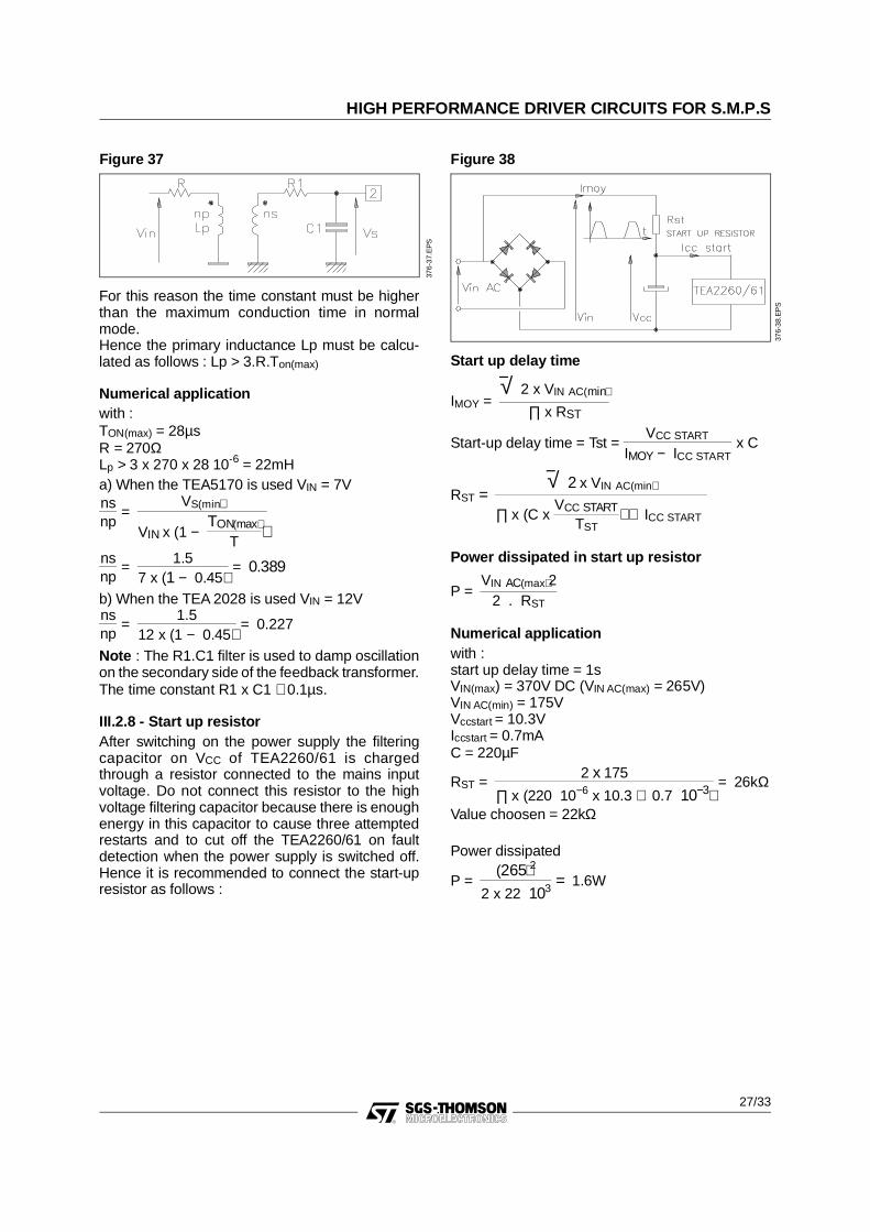
III.2.8 - Start up resistorAfter switching on the power supply the filteringcapacitor on VCC of TEA2260/61 is chargedthrough a resistor connected to the mains inputvoltage. Do not connect this resistor to the highvoltage filtering capacitor because there is enoughenergy in this capacitor to cause three attemptedrestarts and to cut off the TEA2260/61 on faultdetection when the power supply is switched off.Hence it is recommended to connect the start-upresistor as follows :
376-
38.E
PS
Figure 38
Start up delay time
IMOY = √ 2 x VIN AC(min)
∏ x RST
Start-up delay time = Tst = VCC START
IMOY − ICC START x C
RST = √ 2 x VIN AC(min)
∏ x (C x VCC START
TST) + ICC START
Power dissipated in start up resistor
P = VIN AC(max)
22 . RST
Numerical applicationwith :start up delay time = 1sVIN(max) = 370V DC (VIN AC(max) = 265V)VIN AC(min) = 175VVccstart = 10.3VIccstart = 0.7mAC = 220µF
RST = 2 x 175
∏ x (220 10−6 x 10.3 + 0.7 10−3) = 26kΩ
Value choosen = 22kΩ
Power dissipated
P = (265)2
2 x 22 103 = 1.6W
HIGH PERFORMANCE DRIVER CIRCUITS FOR S.M.P.S
27/33

III.2.9 - Determination of high voltage filtering capacitor
376-
39A
.EP
S /
376-
39B
.EP
S
Figure 39
Hypothesis :∆V : ripple on the filtering voltageVIN.AC(min) : minimal value of A.C. input voltageT : period of the mains voltagePout : output power of the power supplyη : efficiency of the power supply
C = T2π
x
π2
+ ArcSin(1 − ∆V
VIN AC(min) x√2)
∆VIN AC(min) x √2 x
POUT
η
Numerical application∆V = 40VVIN AC(min) = 170 VACT = 20msPOUT = 120Wη = 0.85
C = 20 10−3
2π x
π2
+ ArcSin(1 − 40250
)
40 x 250 x 120
0.85 = 115µF
value choosen : C = 120µs
HIGH PERFORMANCE DRIVER CIRCUITS FOR S.M.P.S
28/33

III.3 - Electrical Diagram
Po
wer
pri
mar
y gr
oun
dS
econ
dary
gro
und
(is
ola
ted
from
ma
ins)
Sm
all s
ign
al s
eco
ndar
y gr
oun
d
170
VA
C
270
VA
C
4 x
1N
4007
120µ
F38
5V
BY
218-
600
PLR
811
BY
218
-10
0
BY
218
-100
470
µ F2
5V
100
0µ F
25V
1000
µ F
25V
220µ
F25
V
BA
157
1N41
48 100
pF
2.7n
F1k
VBY299
47µ
F
BZ
X85
-3V
0
2.2µ
H
220 nF
220 nF
1nF
1nF
2.2
µ F
16V
SG
SF
344
313
6
20 19
14
717
9
22
21
12V
135V
7.5V Sta
nd-b
yco
ntro
l
47n
F1.
2nF 2%
1N41
48
150p
FS
ync.
inpu
t
10µ F
16V
18
732
46
5
76
45
1213
1615
11
102
98
31
41
BC
547
C 3.3n
F
TE
A22
60/6
1
Ω12
0k
Ω2.
2k
Ω10
k Ω75 k
ΩΩ
105
k1
%6
.8k
ΩΩ
Ω
1k
560k
8W
ΩΩ
0.17
0
/1W
Ω
Ω
Ω
22k
100k
100
Ω
Ω
Ω
Ω
36
22k
2W
10 1W
Ω1k
Ω1k
Ω
Ω
18k
4.7
k
P2
OU
T
2.2
/0
.5W
47k
Ω
P1
P
:
120W
f
:
16
kHz
25V
270
TE
A51
70
100µ
F2
50V
1833
0 Ω
1 nF
376-
40.E
PS
Figure 40
HIGH PERFORMANCE DRIVER CIRCUITS FOR S.M.P.S
29/33

IV - TV APPLICATION 140W - 220 VAC - 32kHzSYNCHRONIZABLE
All details concerning the determination of externalcomponents are described in section III.
IV.1 - Application Characteristics- Discontinuous mode flyback SMPS- Stand-by function using the burst mode of TEA
2260.- Switching frequency in burst mode : 16kHz - Switching frequency in normal mode : 32kHz- Nominal mains voltage : 220 VAC- Mains voltage range : 170 VAC to 270 VAC- Output power range in normal mode 25W < Po
140W- Output power range in stand-by mode 2W < Po
45W- Efficiency at full load > 80%- Efficiency in stand-by mode (Po = 7W) > 50%- Short circuit protection- Long duration overload protection- Complete shut down after 3 restarts with fault
detection for TEA2260- Complete shut down when VC2 reaches 2.6V for
TEA2261
Load regulation (VDC = 310V)Output 135V (+/- 0.18%) → (I135 : 0.01A to 0.8A;I25 = 1A)Output 25V (+/- 2%) → (I135 : O.8A; I25 = 0.5A to1A)
Line regulation (I135 : 0.8A; I 25 : 1A)Output 135V (+/- 0.13%)→ (210V < VDC < 370V)Output 25V (+/- 0.17%)
IV.2 - Transformer Specification- Reference : OREGA.SMT5. G4576-03- Electrical Data :
Winding Pin Inductance
nP 3-6 790µH
nAUX 7-9 5.4µH
n2 19-13 338µH
n3 19-20 4.8µH
n4 14-17 3.4µH
n5 22-21 13µH
13
20
19
14
3
6
9
7
17
22
21
376-
41.E
PS
Figure 41
HIGH PERFORMANCE DRIVER CIRCUITS FOR S.M.P.S
30/33
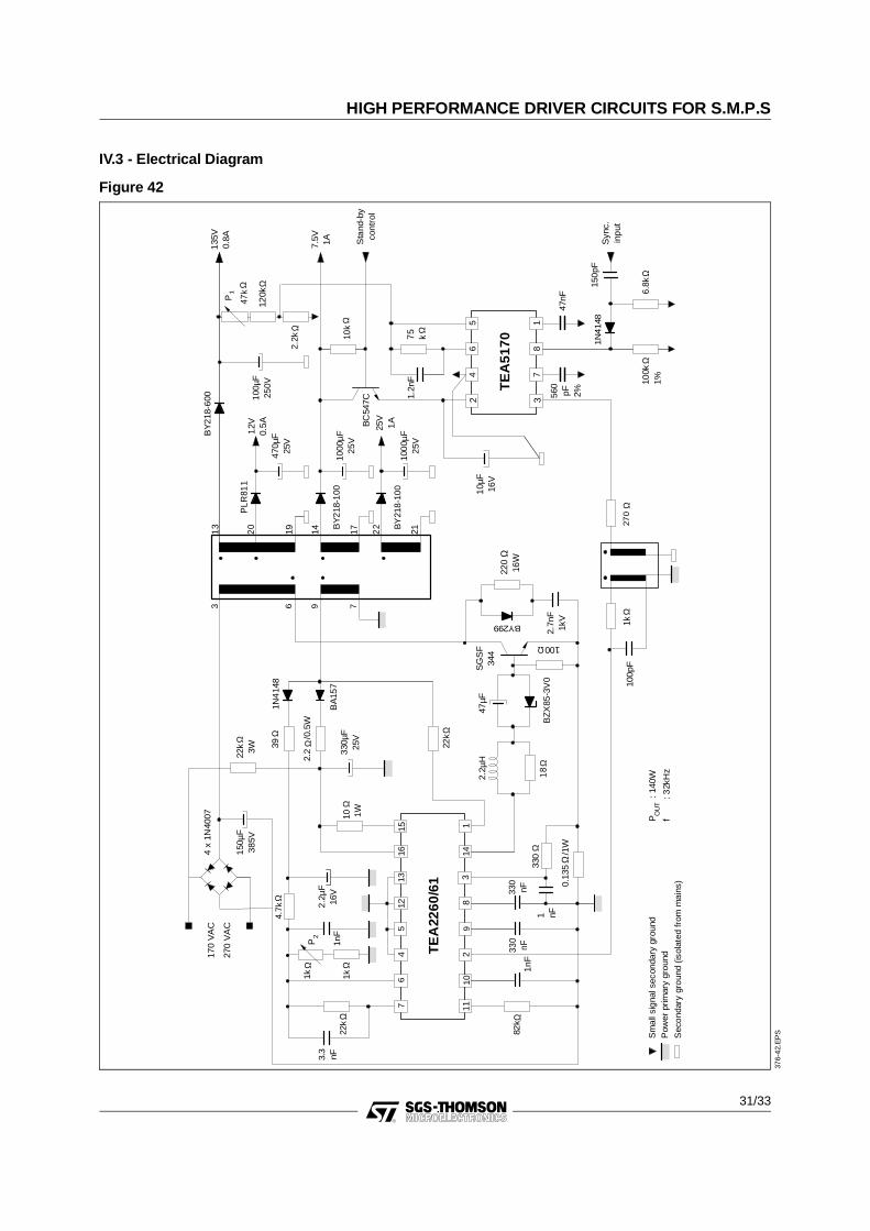
IV.3 - Electrical Diagram
Pow
er p
rimar
y gr
ound
Sec
ond
ary
grou
nd (
isol
ated
from
mai
ns)
Sm
all s
igna
l sec
onda
ry g
roun
d
170
VA
C
270
VA
C
4 x
1N40
07B
Y21
8-60
0
PLR
811
BY
218-
100
BY
218-
100
470µ
F25
V
1000
µ F25
V
1000
µ F25
V
BA
157
1N4
148 10
0pF
2.7n
F1k
VBY299
47µ F
BZ
X85
-3V
0
2.2µ
H
1nF
1nF
2.2µ
F16
V
SG
SF
344
31
3
6
20
19 14
717
9
22
21
Sta
nd-b
yco
ntro
l
47nF
1N414
815
0pF
Syn
c.in
put
10µ
F16
V
18
732
46
5
76
45
1213
1615
1110
29
83
141
BC
547C
TE
A22
60/6
1
TE
A51
70
Ω12
0k
Ω2.
2k
Ω10
k Ω7
5k
ΩΩ
6.8k
ΩΩ
Ω
1k
Ω
Ω
Ω
Ω
Ω
18
22k
100
Ω
Ω
Ω
Ω10 1
W
Ω1k
Ω1k
Ω
Ω4.
7k
P2
OU
T
2.2
/0
.5W
47k
Ω
P1
135V
0.8A
7.5V 1A
12V
0.5A 25
V1
A
1.2n
F
560
pF 2%
100k
1%
220
16W
0.13
5
/1W
330
nF33
0nF
22k
3.3
nF
150µ
F38
5V22
k 3
W 39
330µ
F25
V
P
:
140W
f
: 3
2kH
z
82k
270
100µ
F25
0V
330 Ω
1 nF
376-
42.E
PS
Figure 42
HIGH PERFORMANCE DRIVER CIRCUITS FOR S.M.P.S
31/33

V - TV APPLICATION 110W -220 VAC - 40kHzREGULATED WITH OPTOCOUPLER
This application works in asynchronous mode. Theregulation characteristics are very attractive (out-put power variation range from 1W to 110W due toautomatic burst mode (see II.6). In this configura-tion higher is the regulation loop gain, lower is theoutput voltage ripple in burst mode (e.g. ouputvoltage ripple 0.8% with a loop gain of 15).
V.1 - Frequency Soft StartThe nominal switching frequency is 40kHz but dur-ing the start-up phase the switching frequency isshifted to 10kHz in order to avoid the magnetizationof the transformer.Otherwise the second current limitation will bereached at high input voltage and hence the powersupply will not start.
V.2 - Application Characteristics- Discontinous mode Flyback SMPS- Switching frequency : 40kHz- Nominal mains voltage : 220 VAC- Mains voltage range : 170 VAC to 220 VAC- Output power in normal mode : 30W < Po < 110W- Output power in burst mode :
1W < Po < 30W.The transient phase betweennormal mode and burst mode is determinatedautomatically as a function of the output power.Hence the regulation of the output voltage iseffective for an output power variation of1W < Po < 110W
- Efficiency as full load > 80%- Efficiency in burst mode (Po = 8W) > 50%- Short circuit protection- Open load protection- Long duration overload protection - Complete shutdown after 3 restarts with fault
detection for TEA2260- Complete shut down when VC2 reaches 2.6V for
TEA2261
Load regulation (VDC = 310V)Output 135V (+/- 0.15%) → (I135 : 0.05A to 0.6A;I25 = 1A)Output 25V (+/- 2.5%) →(I135 = 0.6A; I25 : 0.25 to1A)
Line regulation (I135 : 0.6A; I25 : 1A)Output 135V (+/- 0.30%) → (210V < VDC <, 370V)Output 25V (+/- 0.30%)
Influence of the audio output on the video out-putOutput 135V (+/- 0.1%) →(I135 = 0.6A; I25 : 0 →1A)Output 135V (+/- 0.05%) →(I135 = 0.3A; I25 : 0 →1A
V.3 - Transformer S pecification- Reference : OREGA.SMT5. G4576-02- Mechanical Data :
- Ferrite : B50- 2 cores : 53 x 18 x 18(mm) THOMSON LCC
- Electrical Data :
Winding Pin InductancenP 3-6 790µH
nAUX 7-9 5.4µHn2 19-13 338µHn3 19-20 4.8µHn4 14-17 3.4µHn5 22-21 13µH
13
20
19
14
3
6
9
7
17
22
21
376-
43.E
PS
Figure 43
HIGH PERFORMANCE DRIVER CIRCUITS FOR S.M.P.S
32/33

V.4 - Electrical Diagram
Pow
er p
rimar
y gr
ound
Sec
onda
ry g
roun
d (is
olat
ed fr
om m
ains
)
Sm
all s
igna
l sec
onda
ry g
roun
d
170
VA
C
270
VA
C
4 x
1N40
07B
Y21
8-60
0
PLR
811
BY
218-
100
BY
218-
100
470µ
F25
V
BA
157
2.7n
F1k
VBY299
47µ F
BZ
X85
-3V
0
2.2µ
HS
GS
F34
4
313
6
20 19 14
717
9
22 21
76
45
1213
1615
1110
29
83
141
TE
A22
60/6
1
Ω12
0k
Ω Ω
Ω
Ω
Ω
Ω
Ω
18
100
Ω Ω
Ω
Ω
Ω
Ω OU
T
2.2
/0
.5W
25V
1A
220
16W
330µ
F25
V
135V
0.7A
12V
0.5A
39 nF56
0
2.2k
10 2W
45
2.2k
120µ
F38
5V22
k 2
W
1µ F
1µ F
680
pF
Ω 220k
Ω 56k
2.2M
BC
547
27 nF0.
120
/1
W
4.7k
Ω4.
7k
7.5V 1A
BC
547A
1 2
CN
X62
2.2
k BZ
X55
C6V
2
10nF
470µ
F25
V
470µ
F40
V
P
:
110W
f
: 4
0kH
z
100µ
F25
0V
1 nF
330
Ω
376-
44.E
PS
Figure 44
HIGH PERFORMANCE DRIVER CIRCUITS FOR S.M.P.S
33/33

Information furnished is believed to be accurate and reliable. However, SGS-THOMSON Microelectronics assumes no responsibilityfor the consequences of use of such information nor for any infringement of patents or other rights of third parties which may resultfrom its use. No licence is granted by implication or otherwise under any patent or patent rights of SGS-THOMSON Microelectroni cs.Specifications mentioned in this publication are subject to change without notice. This publication supersedes and replaces allinformation previously supplied. SGS-THOMSON Microelectronics products are not authorized for use as critical components in lif esupport devices or systems without express written approval of SGS-THOMSON Microelectronics.
© 1994 SGS-THOMSON Microelectronics - All Rights Reserved
Purchase of I 2C Components of SGS-THOMSON Microelectronics, conveys a license under the PhilipsI2C Patent. Rights to use these components in a I 2C system, is granted provided that the system conforms to
the I2C Standard Specifications as defined by Philips.
SGS-THOMSON Microelectronics GROUP OF COMPANIESAustralia - Brazil - China - France - Germany - Hong Kong - Italy - Japan - Korea - Malaysia - Malta - MoroccoThe Netherlands - Singapore - Spain - Sweden - Switzerland - Taiwan - Thailand - United Kingdom - U.S.A.


![Datalogic SG4 Body Reflector Base & Muting Series Safety ... · l- passive t- passive muting version - passive unit model l1 [mm] l2 [mm] sg4-rdb2 580,5 520,5 sg4-rdb2l 580,5 520,5](https://img.pdfslide.us/doc/110x75/5b50c33f7f8b9a5a6f8f11bf/datalogic-sg4-body-reflector-base-muting-series-safety-l-passive-t-passive.jpg)