Embed Size (px)
Citation preview

Product
Folder
Order
Now
Technical
Documents
Tools &
Software
Support &Community
An IMPORTANT NOTICE at the end of this data sheet addresses availability, warranty, changes, use in safety-critical applications,intellectual property matters and other important disclaimers. PRODUCTION DATA.
TCI6636K2HSPRS835H –FEBRUARY 2012–REVISED OCTOBER 2017
TCI6636K2H Multicore DSP+ARM® KeyStone™ II System-on-Chip (SoC)
1 Device Overview
1
1.1 Features1
• Eight TMS320C66x DSP Core Subsystems (C66xCorePacs), Each With– 1.0 GHz or 1.2 GHz C66x Fixed- and Floating-
Point DSP Core– 38.4 GMacs/Core for Fixed Point @ 1.2 GHz– 19.2 GFlops/Core for Floating Point @ 1.2
GHz– Memory
– 32-KB L1P Per CorePac– 32-KB L1D Per CorePac– 1024-KB Local L2 Per CorePac
• ARM CorePac– Four ARM® Cortex®-A15 MPCore™ Processors
at up to 1.4 GHz– 4MB of L2 Cache Memory Shared by Four ARM
Cores– Full Implementation of ARMv7-A Architecture
Instruction Set– 32-KB L1 Instruction and Data Caches per Core– AMBA 4.0 AXI Coherency Extension (ACE)
Master Port, Connected to MSMC for Low-Latency Access to Shared MSMC SRAM
• Multicore Shared Memory Controller (MSMC)– 6MB of MSM SRAM Memory Shared by Eight
DSP CorePacs and One ARM CorePac– Memory Protection Unit (MPU) for Both MSM
SRAM and DDR3_EMIF• Hardware Coprocessors
– Two Turbo Decoders– Supports WCDMA/HSPA/HSPA+/TD-
SCDMA, LTE, LTE-A, and WiMAX– Supports up to 265 Mbps for LTE at Block
Size 6144, 8 Iterations and up to 200 Mbpsfor WCDMA at Block Size 5114, 8 Iterations
– Low DSP Overhead – Hardware InterleaverTable Generation and CRC Check
– Four Viterbi Decoders– Supports up to 48 Mbps (Length 9, Rate 1/2,
Block Size 6000)– Two WCDMA Receive Acceleration
Coprocessors– Supports up to 4096 Correlators
– WCDMA Transmit Acceleration Coprocessor– Supports up to 2304 Spreaders
– Four Fast Fourier Transform (FFT)Coprocessors– Support up to 600 Mscps/FFTC at FFT Size
1024– Bit Rate Coprocessor
– WCDMA/HSPA+, TD-SCDMA, LTE, LTE-A,and WiMAX Uplink and Downlink BitProcessing
– Includes Encoding, RateMatching/Dematching, Segmentation,Multiplexing, and More
– Supports up to DL 1525 Mbps and UL 1030(on-chip) or 680 (DDR3) Mbsp for LTE andDL 784 Mbps and UL 395 Mbsp forWCDMA/TD-SCDMA
• Multicore Navigator– 16k Multipurpose Hardware Queues With
Queue Manager– Packet-Based DMA for Zero-Overhead
Transfers• Network Coprocessor
– Packet Accelerator Enables Support for– Transport Plane IPsec, GTP-U, SCTP, PDCP– L2 User Plane PDCP (RoHC, Air Ciphering)– 1-Gbps Wire Speed Throughput at 1.5
MPackets Per Second– Security Accelerator Engine Enables Support for
– IPSec, SRTP, 3GPP, and WiMAX AirInterface, and SSL/TLS Security
– ECB, CBC, CTR, F8, A5/3, CCM, GCM,HMAC, CMAC, GMAC, AES, DES, 3DES,Kasumi, SNOW 3G, SHA-1, SHA-2 (256-BitHash), MD5
– Up to 2.4 Gbps IPSec and 2.4 Gbps AirCiphering
– Ethernet Subsystem– Five-Port Switch (Four SGMII Ports)
• Sixteen Rake/Search Accelerators (RSA) for– Chip Rate Processing for WCDMA Rel'99,
HSDPA, and HSDPA+– Reed-Muller Decoding

2
TCI6636K2HSPRS835H –FEBRUARY 2012–REVISED OCTOBER 2017 www.ti.com
Submit Documentation FeedbackProduct Folder Links: TCI6636K2H
Device Overview Copyright © 2012–2017, Texas Instruments Incorporated
• Peripherals– Six-Lane SerDes-Based Antenna Interface
(AIF2)– Operating at up to 6.144 Gbps– Compliant With OBSAI RP3 and CPRI
Standards for 3G and 4G (WCDMA, LTETDD, LTE FDD, TD-SCDMA, and WiMAX)
– Four Lanes of SRIO 2.1– Supports up to 5 GBaud– Supports Direct I/O, Message Passing
– Two Lanes PCIe Gen2– Supports up to 5 GBaud
– Two HyperLinks– Supports Connections to Other KeyStone™
Architecture Devices Providing ResourceScalability
– Supports up to 50 GBaud
– Five Enhanced Direct Memory Access (EDMA)Modules
– Two 72-Bit DDR3/DDR3L Interfaces WithSpeeds up to 1600 MHz
– EMIF16 Interface– USB 3.0– USIM Interface– Two UART Interfaces– Three I2C Interfaces– 32 GPIO Pins– Three SPI Interfaces– Semaphore Module– Twenty 64-Bit Timers– Five On-Chip PLLs
• Commercial Case Temperature:– 0ºC to 100ºC
• Extended Case Temperature:– –40ºC to 100ºC
1.2 Applications• Small Cell
1.3 DescriptionThe TCI6636K2H Communications Infrastructure KeyStone SoC is a member of the C66x family based onTI's new KeyStone II Multicore SoC Architecture designed specifically for high-performance wirelessinfrastructure applications. The TCI6636K2H provides a very high-performance macro base stationplatform for developing all wireless standards, including WCDMA/HSPA/HSPA+, TD-SCDMA, GSM, TDD-LTE, FDD-LTE, and WiMAX.
TI's KeyStone II Architecture provides a programmable platform integrating various subsystems (ARMCorePac, C66x CorePacs, IP network, radio layers 1, 2, and 3, and transport processing) and uses aqueue-based communication system that allows the SoC resources to operate efficiently and seamlessly.This unique SoC architecture also includes a TeraNet switch that enables the wide mix of systemelements, from programmable cores to dedicated coprocessors and high-speed I/O, to each operate atmaximum efficiency with no blocking or stalling.
The addition of the ARM CorePac in the TCI6636K2H enables the ability for layer 2 and layer 3processing on-chip. Operations such as Traffic Control, Local O&M, NBAP/FP termination, and SCTPprocessing can all be performed with the Cortex-A15 processor.
TI's new C66x core launches a new era of DSP technology by combining fixed-point and floating-pointcomputational capability in the processor without sacrificing speed, size, or power consumption. The rawcomputational performance is an industry-leading 38.4 GMACS/core and 19.2 Gflops/core (@ 1.2 GHzoperating frequency). The C66x is also 100% backward compatible with software for C64x+ devices. TheC66x CorePac incorporates 90 new instructions targeted for floating point (FPi) and vector math-oriented(VPi) processing. These enhancements yield tremendous performance improvements in multi-antenna4.8G signal processing for algorithms like MIMO and beamforming.
The TCI6636K2H contains many wireless base station coprocessors to offload the bulk of the processingdemands of layer 1 and layer 2 base station processing. This keeps the cores free for receiver algorithmsand other differentiating functions. The SoC contains multiple copies of key coprocessors such as theFFTC and TCP3d. A key coprocessor for enabling high data rates is the Bit Rate Coprocessor (BCP),which handles the entire downlink bit-processing chain and much of the receive bit processing. Thearchitectural elements of the SoC (Multicore Navigator) ensure that all the bits are processed without anyCPU intervention or overhead, allowing the system to make optimal use of its resources.

3
TCI6636K2Hwww.ti.com SPRS835H –FEBRUARY 2012–REVISED OCTOBER 2017
Submit Documentation FeedbackProduct Folder Links: TCI6636K2H
Device OverviewCopyright © 2012–2017, Texas Instruments Incorporated
(1) For more information, see Section 13, Mechanical, Packaging, and Orderable Information.
TI's scalable multicore SoC architecture solutions provide developers with a range of software-compatibleand hardware-compatible devices to minimize development time and maximize reuse across all basestation platforms from Femto to Macro.
The TCI6636K2H device has a complete set of development tools that includes: a C compiler, anassembly optimizer to simplify programming and scheduling, and a Windows® debugger interface forvisibility into source code execution.
1.3.1 KeyStone ArchitectureTI’s KeyStone Multicore Architecture provides a high-performance structure for integrating RISC and DSPcores with application-specific coprocessors and I/O. KeyStone is the first architecture that providesadequate internal bandwidth for nonblocking access to all processing cores, peripherals, coprocessors,and I/O. This accomplishment is achieved with four main hardware elements: Multicore Navigator,TeraNet, Multicore Shared Memory Controller, and HyperLink.
Multicore Navigator is an innovative packet-based manager that controls 16k queues. When tasks areallocated to the queues, Multicore Navigator provides hardware-accelerated dispatch that directs tasks tothe appropriate available hardware. The packet-based system on a chip (SoC) uses the 2-Tbps capacityof the TeraNet switched central resource to move packets. The Multicore Shared Memory Controllerenables processing cores to access shared memory directly without drawing from the capacity of theTeraNet, so packet movement cannot be blocked by memory access.
HyperLink provides a 50-GBaud chip-level interconnect that lets SoCs work in tandem. The low-protocoloverhead and high throughput of HyperLink make it an ideal interface for chip-to-chip interconnections.Working with Multicore Navigator, HyperLink dispatches tasks to tandem devices transparently andexecutes tasks as if they are running on local resources.
1.3.2 Enhancements in KeyStone IIThe KeyStone II architecture provides many major enhancements over the previous KeyStone Igeneration of devices. The KeyStone II architecture integrates an ARM Cortex-A15 processor quad-corecluster to enable Layer 2 (MAC/RLC) and higher layer processing. The number of DSP cores and FFTCaccelerators has been doubled, thus doubling the processing speed of Layer 1. The external memorybandwidth has been doubled with the integration of dual DDR3 1600 EMIFs. MSMC internal memorybandwidth is quadrupled with MSMC V2 architecture improvements. Multicore Navigator supports twicethe number of queues, descriptors, and packet DMA, four times the number of micro RISC engines, and asignificant increase in the number of push/pops per second, compared to the previous generation. Thenew peripherals that have been added include the USB 3.0 controller, USIM interface controller, andAsynchronous EMIF controller for NAND/NOR memory access. The 2-port Gigabit Ethernet switch inKeyStone I has been replaced with a 4-port Gigabit Ethernet switch in KeyStone II. Time synchronizationsupport has been enhanced to reduce software workload and support additional standards like IEEE 1588Annex D/E and SyncE. The number of GPIOs and serial interface peripherals like I2C and SPI have beenincreased to enable more board level control functionality.
Device Information (1)
PART NUMBER PACKAGE BODY SIZETCI6636K2H AAW 40.0 mm × 40.0 mm

Coprocessors
BCP
PacketDMA
Multicore Navigator
QueueManager
Debug & Trace
5´
PLL
Semaphore
2´ HyperLink TeraNet
TAC
2´TCP3d
4´
VCP2
2´RAC
4´
FFTC
5´
EDMA
8´Boot ROM
PowerManagement
ARMA15
4MB L2 Cache
32KB L1P-Cache
32KB L1D-Cache
32KB L1P-Cache
32KB L1D-Cache
ARMA15
32KB L1P-Cache
32KB L1D-Cache
ARMA15
32KB L1P-Cache
32KB L1D-Cache
ARMA15
SR
IO4
´
AIF
26
´
3´
SP
I
2´
UA
RT
PC
Ie2
´
3´
IC
2
GP
IO32
´
Oth
ers
MSMC
6MBMSM
SRAM
72-BitDDR3 EMIF
Memory Subsystem
72-BitDDR3 EMIF
TCI6636K2H
US
B 3
.0
32KB L1P-Cache
32KB L1D-Cache
C66x™CorePac
1024KB L2 Cache
RSA RSA
32KB L1P-Cache
32KB L1D-Cache
C66x™CorePac
1024KB L2 Cache
RSA RSA
32KB L1P-Cache
32KB L1D-Cache
C66x™CorePac
1024KB L2 Cache
RSA RSA
32KB L1P-Cache
32KB L1D-Cache
C66x™CorePac
1024KB L2 Cache
RSA RSA
32KB L1P-Cache
32KB L1D-Cache
C66x™CorePac
1024KB L2 Cache
RSA RSA
32KB L1P-Cache
32KB L1D-Cache
C66x™CorePac
1024KB L2 Cache
RSA RSA
32KB L1P-Cache
32KB L1D-Cache
C66x™CorePac
1024KB L2 Cache
RSA RSA
32KB L1P-Cache
32KB L1D-Cache
C66x™CorePac
1024KB L2 Cache
RSA RSA
EM
IF16
US
IM
8 C66x DSP Cores @ up to 1.2 GHz4 ARM Cores @ up to 1.4 GHz
NetworkCoprocessor
5-PortEthernetSwitch
PacketAccelerator
SecurityAccelerator
1G
BE
1G
BE
1G
BE
1G
BE
Copyright © 2016, Texas Instruments Incorporated
4
TCI6636K2HSPRS835H –FEBRUARY 2012–REVISED OCTOBER 2017 www.ti.com
Submit Documentation FeedbackProduct Folder Links: TCI6636K2H
Table of Contents Copyright © 2012–2017, Texas Instruments Incorporated
1.4 Functional Block DiagramFigure 1-1 shows the functional block diagram of the device.
Figure 1-1. Functional Block Diagram
Table of Contents1 Device Overview ......................................... 1
1.1 Features .............................................. 11.2 Applications........................................... 21.3 Description............................................ 21.4 Functional Block Diagram ............................ 4
2 Revision History ......................................... 63 Device Comparison ..................................... 7
3.1 Related Products ..................................... 84 Terminal Configuration and Functions.............. 9
4.1 Package Terminals ................................... 94.2 Pin Map............................................... 94.3 Terminal Functions.................................. 144.4 Pullup/Pulldown Resistors .......................... 48
5 Specifications ........................................... 505.1 Absolute Maximum Ratings ......................... 505.2 ESD Ratings ........................................ 505.3 Recommended Operating Conditions............... 515.4 Power Consumption Summary...................... 51

5
TCI6636K2Hwww.ti.com SPRS835H –FEBRUARY 2012–REVISED OCTOBER 2017
Submit Documentation FeedbackProduct Folder Links: TCI6636K2H
Table of ContentsCopyright © 2012–2017, Texas Instruments Incorporated
5.5 Electrical Characteristics ............................ 525.6 Thermal Resistance Characteristics for PBGA
Package [AAW] ..................................... 525.7 Power Supply to Peripheral I/O Mapping ........... 53
6 C66x CorePac ........................................... 546.1 C66x DSP CorePac ................................. 556.2 Memory Architecture ................................ 556.3 Memory Protection .................................. 586.4 Bandwidth Management ............................ 596.5 Power-Down Control ................................ 596.6 C66x CorePac Revision............................. 606.7 C66x CorePac Register Descriptions ............... 60
7 ARM CorePac ........................................... 617.1 Features ............................................. 627.2 System Integration .................................. 627.3 ARM Cortex-A15 Processor......................... 627.4 CFG Connection .................................... 647.5 Main TeraNet Connection........................... 647.6 Clocking and Reset ................................. 64
8 Memory, Interrupts, and EDMA for TCI6636K2H. 658.1 Memory Map Summary for TCI6636K2H ........... 658.2 Memory Protection Unit (MPU)...................... 758.3 Interrupts ............................................ 898.4 Enhanced Direct Memory Access (EDMA3)
Controller for TCI6636K2H......................... 1529 System Interconnect ................................. 163
9.1 Internal Buses and Switch Fabrics ................ 1639.2 Switch Fabric Connections Matrix - Data Space .. 1639.3 TeraNet Switch Fabric Connections Matrix -
Configuration Space ............................... 1739.4 Bus Priorities....................................... 181
10 Device Boot and Configuration.................... 18210.1 Device Boot ........................................ 18210.2 Device Configuration............................... 206
11 TCI6636K2H Peripheral Information .............. 23711.1 Recommended Clock and Control Signal Transition
Behavior............................................ 23711.2 Power Supplies .................................... 23711.3 Power Sleep Controller (PSC) ..................... 24511.4 Reset Controller.................................... 25111.5 Main PLL, ARM PLL, DDR3A PLL, DDR3B PLL,
PASS PLL and the PLL Controllers................ 25711.6 DDR3A PLL and DDR3B PLL ..................... 272
11.7 PASS PLL.......................................... 27511.8 External Interrupts ................................. 27711.9 DDR3A and DDR3B Memory Controllers.......... 27811.10 I2C Peripheral..................................... 28011.11 SPI Peripheral .................................... 28411.12 HyperLink Peripheral ............................. 28711.13 UART Peripheral ................................. 28911.14 PCIe Peripheral................................... 29011.15 Packet Accelerator ............................... 29011.16 Security Accelerator .............................. 29111.17 Network Coprocessor Gigabit Ethernet (GbE)
Switch Subsystem ................................. 29111.18 SGMII Management Data Input/Output (MDIO) .. 29211.19 Timers............................................. 29311.20 Rake Search Accelerator (RSA).................. 29411.21 Enhanced Viterbi-Decoder Coprocessor (VCP2). 29411.22 Turbo Decoder Coprocessor (TCP3d)............ 29511.23 Turbo Encoder Coprocessor (TCP3e)............ 29511.24 Bit Rate Coprocessor (BCP)...................... 29511.25 Serial RapidIO (SRIO) Port ....................... 29511.26 General-Purpose Input/Output (GPIO) ........... 29611.27 Semaphore2 ...................................... 29711.28 Antenna Interface Subsystem 2 (AIF2)........... 29711.29 Receive Accelerator Coprocessor (RAC) ....... 29911.30 Transmit Accelerator Coprocessor (TAC) ........ 30011.31 Fast Fourier Transform Coprocessor (FFTC) ... 30011.32 Universal Serial Bus 3.0 (USB 3.0)............... 30011.33 Universal Subscriber Identity Module (USIM) .... 30011.34 EMIF16 Peripheral................................ 30011.35 Emulation Features and Capability ............... 30311.36 Debug Port (EMUx) ............................... 306
12 Device and Documentation Support.............. 31612.1 Device Nomenclature .............................. 31612.2 Tools and Software ................................ 31812.3 Documentation Support............................ 31912.4 Community Resources............................. 32412.5 Trademarks ........................................ 32412.6 Electrostatic Discharge Caution ................... 32412.7 Glossary............................................ 324
13 Mechanical, Packaging, and OrderableInformation ............................................. 32513.1 Packaging Information ............................. 325

6
TCI6636K2HSPRS835H –FEBRUARY 2012–REVISED OCTOBER 2017 www.ti.com
Submit Documentation FeedbackProduct Folder Links: TCI6636K2H
Revision History Copyright © 2012–2017, Texas Instruments Incorporated
2 Revision HistoryNOTE: Page numbers for previous revisions may differ from page numbers in the current version.
Changes from Revision G (May 2017) to Revision H Page
• Added DDR3L Interface to Features. .............................................................................................. 2• Updated DVDD15 power supply in Terminal Functions — Power and Ground table from 1.5 V to 1.35/1.5 V......... 30• Updated DVDD15 entry in Recommended Operating Conditions table. .................................................... 51• Updated DVDD15 power supply in Power Supply to Peripheral I/O Mapping table, from 1.5 V to 1.35/1.5 V. ........ 53• Updated Equation. ................................................................................................................ 205• Added Footnote to System PLL Configuration table. ......................................................................... 206• Added Footnote to ARM PLL Configuration table. ............................................................................ 206• Added DSP Boot Address Register (DSP_BOOT_ADDRn). ................................................................ 213• Updated DVDD15 value in Power Supply Rails table from 1.5 V to 1.35/1.5V. ........................................... 237• Updated DDR3 value in DDR3 Memory Controller Device-Specific Information section from 1.5-V to 1.35-V /
1.5-V. ............................................................................................................................... 278• Updated Timers Device-Specific Information section. ....................................................................... 293

7
TCI6636K2Hwww.ti.com SPRS835H –FEBRUARY 2012–REVISED OCTOBER 2017
Submit Documentation FeedbackProduct Folder Links: TCI6636K2H
Device ComparisonCopyright © 2012–2017, Texas Instruments Incorporated
(1) The USIM is implemented for support of secure devices only. Contact your local technical sales representative for further details(2) The Security Accelerator function is subject to export control and will be enabled only for approved device shipments.
3 Device Comparison
Table 3-1 provides an overview of the TCI6636K2H device. The table lists the significant features of thedevice, including the capacity of on-chip RAM, the peripherals, the CPU frequency, and the package typewith pin count.
Table 3-1. Device Features Comparison
HARDWARE FEATURES TCI6636K2H
CoresC66x DSP 8ARM Cortex-A15 MPCore 4
Peripherals
DDR3 memory controller (72-bit bus width) [1.5 V I/O](clock source = DDRREFCLKN|P)
2
16-bit ASYNC EMIF 1EDMA3 (64 independent channels) [CPU/3 clock rate] 5High-speed 1×/2×/4× Serial RapidIO port (4 lanes) 1HyperLink (4 lanes) 2AIF2 (Second generation Antenna Interface) (6 lanes) 1I2C 3SPI 3PCIe (2 lanes) 1USB 3.0 1USIM (1) 1UART 210/100/1000 Ethernet 4Management Data Input/Output (MDIO) 164-bit timers (configurable) (internal clock source = CPU/6clock frequency)
Twenty 64-bit or Forty 32-bit
General-Purpose Input/Output port (GPIO) 32
Encoder/DecoderCoprocessors
VCP2 (clock source = CPU/3 clock frequency) 4TCP3d (clock source = CPU/2 clock frequency) 2FFTC (clock source = CPU/3 clock frequency) 4BCP (clock source = CPU/3 clock frequency) 1
Accelerators
Receive Accelerator (RAC) 2Transmit Accelerator (TAC) 1Rake/Search Accelerator (RSA) 16Packet Accelerator 1Security Accelerator (2) 1
On-Chip MemoryOrganization
L1 program memory controller (C66x) 32KB per CorePacL1 data memory controller (C66x) 32KB per CorePacShared L2 cache (C66x 8192KBL3 ROM (C66x) 128KBL1 program memory controller (ARM Cortex-A15) 32KB per CorePacL1 data memory controller (ARM Cortex-A15) 32KB per CorePacShared L2 cache (ARM Cortex-A15) 4096KBL3 ROM (ARM Cortex-A15) 256KBMSMC 6MB

8
TCI6636K2HSPRS835H –FEBRUARY 2012–REVISED OCTOBER 2017 www.ti.com
Submit Documentation FeedbackProduct Folder Links: TCI6636K2H
Device Comparison Copyright © 2012–2017, Texas Instruments Incorporated
Table 3-1. Device Features Comparison (continued)HARDWARE FEATURES TCI6636K2H
C66x CorePacRevision ID
CorePac Revision ID Register (address location: 01812000h)
0x0009_0000 (PG 1.0)0x0009_0002 (PG 1.1)0x0009_0003 (PG 2.0)0x0009_0003 (PG 3.0)0x0009_0003 (PG 3.1)
JTAG BSDL_ID JTAGID Register (address location: 0x02620018)
0x0b98102f (PG 1.0)0x1b98102f (PG 1.1)0x2b98102f (PG 2.0)0x3b98102f (PG 3.0)0xbb98102f (PG 3.1)
FrequencyC66x Up to 1.2 GHzARM Cortex-A15 Up to 1.4 GHz
VoltageCore (V) SmartReflex™ variable supplyI/O (V) 0.85 V, 1.0 V, 1.5 V, 1.8 V, and 3.3 V
BGA Package 40 mm × 40 mm AAW 1517-pin flip-chip plastic BGAProcess Technology µm 0.028 µm
3.1 Related ProductsFor information about other devices in this family of products or related products, see the following links.Digital Signal Processors From sensors to servers, TI has the right DSPs for every application.Communications Processors Cost-effective and operationally efficient wireless communication systems
are required by markets like small cells, C-RAN, public safety, military and tacticalcommunications, software defined radio and wireless backhaul. TI provides a range of highperformance, scalable, low-power baseband solutions that meet the stringent power, sizeand bill of materials (BOM) cost requirements of a wide range of communicationsinfrastructure equipment.
Companion Products for TCI6636K2H Review products that are frequently purchased or used inconjunction with this product.

A B C D
9
TCI6636K2Hwww.ti.com SPRS835H –FEBRUARY 2012–REVISED OCTOBER 2017
Submit Documentation FeedbackProduct Folder Links: TCI6636K2H
Terminal Configuration and FunctionsCopyright © 2012–2017, Texas Instruments Incorporated
4 Terminal Configuration and Functions
4.1 Package TerminalsFigure 4-1 shows the AAW ball grid array package (bottom view).
Figure 4-1. AAW 1517-Pin BGA Package (Bottom View)
4.2 Pin MapThe following figures show the TCI636K2H pin assignments in four quadrants (A, B, C, and D).
Figure 4-2. Pin Map Panels (Bottom View)

10
TCI6636K2HSPRS835H –FEBRUARY 2012–REVISED OCTOBER 2017 www.ti.com
Submit Documentation FeedbackProduct Folder Links: TCI6636K2H
Terminal Configuration and Functions Copyright © 2012–2017, Texas Instruments Incorporated
1 2 3 4 5 6 7 8 9 10AW (NOPIN) VSS VSS MCM1CLKP MCM1CLKN VSS MCM0RXN3 MCM0RXP3 VSS MCM0RXN0
AV VSS VSS MCM1RXN3 MCM1RXP3 VSS MCM1RXN1 MCM1RXP1 VSS MCM0RXN2 MCM0RXP2
AU VSS VSS VSS MCM1RXN2 MCM1RXP2 VSS MCM1RXN0 MCM1RXP0 VSS MCM0RXN1
AT RP1FBN VSS MCM1TXN3 MCM1TXP3 VSS MCM1TXN0 MCM1TXP0 VSS MCM0CLKP MCM0CLKN
AR RP1FBP RP1CLKP VSS MCM1TXN2 MCM1TXP2 VSS MCM0TXN3 MCM0TXP3 VSS MCM0TXN1
AP TSRXCLKOUT0N RP1CLKN TSRXCLKOUT1N VSS MCM1TXN1 MCM1TXP1 VSS MCM0TXN2 MCM0TXP2 VSS
AN TSRXCLKOUT0P VSS TSRXCLKOUT1P RSV002 VSS VSS VSS VSS VSS RSV019
AM TSREFCLKP ALTCORECLKP VSS RSV003 CVDD MCM1REFRES RSV020 VSS MCM0REFRES VSS
AL TSREFCLKN ALTCORECLKN SYSCLKP CORECLKSEL VSS CVDD VSS CVDD VSS VDDAHV
AK SYSCLKOUT VSS SYSCLKN POR RSV012 VSS CVDD VSS CVDD VSS
AJ MCM0TXPMDAT MCM0RXPMCLK MCM0TXFLCLK MCM0RXFLDAT MCM0RXFLCLK VSS VSS CVDD VSS CVDD
AH MCM1TXPMCLK MCM1TXFLDAT MCM1TXFLCLK MCM1RXFLCLK MCM0TXPMCLK VSS VSS VSS CVDD VSS
AG TDI MCM1RXFLDAT MCM0RXPMDAT VSS MCM0TXFLDAT DVDD18 VSS CVDD VSS CVDD
AF TDO MCM1TXPMDAT MCM1RXPMCLK MCM1RXPMDAT BOOTCOMPLETE VSS DVDD18 VSS CVDD VSS
AE TCK TMS VSS LRESET HOUT DVDD18 VSS CVDD VSS CVDD
AD TRST RESET RESETFULL LRESETNMIEN NMI VSS DVDD18 VSS CVDD VSS
AC TSPUSHEVT1 TSPUSHEVT0 TSSYNCEVT EXTFRAMEEVENT RESETSTAT DVDD18 VSS CVDD VSS CVDD
AB TSCOMPOUT EMU01 EMU14 EMU10 DVDD18 VSS DVDD18 VSS CVDD VSS
AA USBRESREF EMU00 EMU11 EMU18 VSS DVDD18 VSS CVDD VSS CVDD
Y USBRX0M VSS EMU02 EMU03 DVDD18 VSS DVDD18 VSS CVDD VSS
W USBRX0P USBCLKP EMU04 EMU05 VSS DVDD18 VSS CVDD VSS CVDD
V USBTX0M USBCLKM VSS EMU06 DVDD18 VSS DVDD18 VSS CVDD VSS
U USBTX0P USBDP EMU08 EMU07 EMU12 DVDD18 VSS CVDD VSS CVDD
T USBVBUS USBDM EMU09 EMU13 EMU16 VSS DVDD18 VSS CVDD VSS
R USBID0 VSS EMU15 EMU17 VSS DVDD18 VSS CVDD VSS CVDD
P RSV001 RSV000 SDA0 SCL2 VSS VSS CVDD VSS CVDD VSS
N SCL0 SDA1 SDA2 SCL1 VSS CVDD VSS CVDD VSS CVDD
M TIMI1 TIMI0 TIMO0 TIMO1 UART1RTS VSS CVDD VSS CVDD VSS
L UART0CTS UART1RXD USBDRVVBUS UART0RTS VSS CVDD VSS DVDD15 VSS DVDD15
K UART1CTS UART0TXD UART1TXD UART0RXD VSS VSS DVDD15 VSS DVDD15 VSS
J VSS VSS VSS VSS VSS DVDD15 VSS DVDD15 VSS DVDD15
H DDR3AD04 DDR3AD01 DDR3AD13 VSS DDR3AD17 VSS DVDD15 VSS DVDD15 DDR3ARZQ1
G DDR3AD00 DDR3AD03 DDR3AD10 DDR3AD16 DDR3AD20 DDR3AD29 DDR3AD30 DDR3AA02 DDR3AA01 DDR3AA03
F DDR3AD02 DDR3AD06 DDR3ADQM1 DDR3AD09 DDR3AD19 DDR3AD26 DDR3AD25 DDR3AA05 DDR3AA04 DDR3AA10
E DDR3ADQS0P DDR3AD05 VSS DDR3AD08 VSS DDR3ADQM3 VSS DDR3AA00 VSS DDR3AA12
D DDR3ADQS0N DDR3AD07 DDR3AD14 DDR3AD15 DDR3AD18 DDR3AD21 DDR3AD31 DDR3AA09 DDR3AA07 DDR3AA15
C VSS DDR3ADQM0 DDR3ADQS1N VSS DDR3AD22 VSS DDR3AD24 VSS DDR3AA06 VSS
B VSS VSS DDR3ADQS1P DDR3AD12 DDR3ADQS2N DDR3AD23 DDR3ADQS3P DDR3AD28 DDR3AA08 DDR3AA14
A (NOPIN) VSS VSS DDR3AD11 DDR3ADQS2P DDR3ADQM2 DDR3ADQS3N DDR3AD27 DDR3AA11 DDR3AA13
1 2 3 4 5 6 7 8 9 10
Figure 4-3. TCI636K2H Pin Map Left Side Panel (A) — Bottom View

11
TCI6636K2Hwww.ti.com SPRS835H –FEBRUARY 2012–REVISED OCTOBER 2017
Submit Documentation FeedbackProduct Folder Links: TCI6636K2H
Terminal Configuration and FunctionsCopyright © 2012–2017, Texas Instruments Incorporated
11 12 13 14 15 16 17 18 19 20AW MCM0RXP0 VSS AIFRXN3 AIFRXP3 VSS AIFRXN0 AIFRXP0 VSS RSV065 RSV064
AV VSS AIFRXN5 AIFRXP5 VSS AIFRXN2 AIFRXP2 VSS RSV061 RSV060 VSS
AU MCM0RXP1 VSS AIFRXN4 AIFRXP4 VSS AIFRXN1 AIFRXP1 VSS RSV070 RSV071
AT VSS AIFTXN5 AIFTXP5 VSS AIFTXN2 AIFTXP2 VSS RSV063 RSV062 VSS
AR MCM0TXP1 VSS AIFTXN4 AIFTXP4 VSS AIFTXN1 AIFTXP1 VSS RSV067 RSV066
AP MCM0TXN0 MCM0TXP0 VSS AIFTXN3 AIFTXP3 VSS AIFTXN0 AIFTXP0 VSS VSS
AN VSS VSS VSS VSS VSS RSV068 VSS VSS RSV026 VSS
AM AIFREFRES1 VSS VSS RSV025 AIFREFRES0 RSV024 VSS VSS RSV069 VSS
AL VSS VDDAHV VSS VDDAHV VSS VDDAHV VSS VDDAHV VSS VDDAHV
AK VDDAHV VSS VDDAHV VSS VDDAHV VSS VDDAHV VSS VDDAHV VSS
AJ VSS VDDALV VSS VDDALV VSS VDDALV VSS VDDALV VSS VDDALV
AH VDDALV VSS VDDALV VSS VDDALV VSS VDDALV VSS VDDALV VSS
AG VSS VDDALV VSS VDDALV VSS VDDALV VSS VDDALV VSS VDDALV
AF AVDDA1 VSS VDDALV VSS VDDALV VSS VDDALV VSS VDDALV VSS
AE VSS CVDD VSS CVDD VSS CVDD VSS CVDD VSS CVDD
AD VNWA2 VSS CVDD VSS CVDD VSS CVDD1 VSS CVDD1 VSS
AC VSS CVDD VSS CVDD VSS CVDD VSS CVDD1 VSS CVDD
AB CVDD VSS VDDUSB VSS CVDD VSS CVDD VSS CVDD VSS
AA VSS VP VSS DVDD33 VSS CVDD VSS CVDD VSS CVDD
Y VPTX VSS VPH VSS CVDD VSS CVDD VSS CVDD VSS
W VSS CVDD VSS CVDD VSS CVDD1 VSS CVDD VSS CVDD
V VNWA4 VSS CVDD1 VSS CVDD VSS CVDD1 VSS CVDD VSS
U VSS CVDD VSS CVDD1 VSS CVDD1 VSS CVDD VSS CVDD1
T CVDD VSS CVDD1 VSS CVDD VSS CVDD VSS CVDD VSS
R VSS CVDD VSS CVDD VSS CVDD VSS CVDD VSS CVDD
P AVDDA6 VSS CVDD VSS CVDD VSS CVDD VSS CVDD VSS
N VSS CVDD VSS CVDD VSS CVDD VSS CVDD VSS AVDDA2
M DVDD15 VSS AVDDA7 VSS AVDDA8 VSS DVDD15 AVDDA9 DVDD15 AVDDA10
L VSS DVDD15 VSS DVDD15 VSS DVDD15 VSS DVDD15 VSS DVDD15
K DVDD15 VSS DVDD15 VSS DVDD15 VSS DVDD15 VSS DVDD15 VSS
J VSS DVDD15 VSS DVDD15 VSS DVDD15 VSS DVDD15 VSS DVDD15
H DVDD15 VSS DVDD15 VSS DVDD15 DDR3ARZQ0 DVDD15 VSS DVDD15 VSS
G DDR3ABA2 DDR3ACKE0 DDR3AODT1 DDR3AVREFSSTL DDR3ACB07 DDR3AD33 DDR3AD35 DDR3AD42 DDR3AD44 DDR3AD51
F DDR3ACE1 DDR3AWE RSV029 DDR3ACB05 DDR3ACB03 DDR3AD34 DDR3AD38 DDR3AD47 DDR3AD43 DDR3AD54
E VSS DDR3AODT0 VSS DDR3ADQM8 VSS DDR3AD32 VSS DDR3AD39 VSS DDR3AD53
D DDR3ACE0 RSV027 RSV028 DDR3ACB06 DDR3ACB04 DDR3AD36 DDR3AD37 DDR3AD46 DDR3AD41 DDR3AD50
C DDR3ABA1 VSS DDR3ACAS VSS DDR3ACB01 VSS DDR3ADQM4 VSS DDR3AD40 VSS
B DDR3ABA0 DDR3ACLKOUTN0 DDR3ACLKOUTN1 DDR3ARESET DDR3ADQS8P DDR3ACB02 DDR3ADQS4N DDR3AD45 DDR3ADQS5P DDR3AD49
A DDR3ACKE1 DDR3ACLKOUTP0 DDR3ACLKOUTP1 DDR3ARAS DDR3ADQS8N DDR3ACB00 DDR3ADQS4P DDR3ADQM5 DDR3ADQS5N DDR3AD48
11 12 13 14 15 16 17 18 19 20
Figure 4-4. TCI636K2H Pin Map Left Center Panel (B) — Bottom View

12
TCI6636K2HSPRS835H –FEBRUARY 2012–REVISED OCTOBER 2017 www.ti.com
Submit Documentation FeedbackProduct Folder Links: TCI6636K2H
Terminal Configuration and Functions Copyright © 2012–2017, Texas Instruments Incorporated
21 22 23 24 25 26 27 28 29 30VSS RIORXN2 RIORXP2 VSS SGMII3RXN SGMII3RXP VSS SGMII0RXN SGMII0RXP VSS AW
RIORXN3 RIORXP3 VSS RIORXN0 RIORXP0 VSS SGMII1RXN SGMII1RXP VSS PCIERXN1 AVVSS RIORXN1 RIORXP1 VSS SGMII2RXN SGMII2RXP VSS SGMII0TXN SGMII0TXP VSS AU
RIOTXN3 RIOTXP3 VSS RIOTXN0 RIOTXP0 VSS SGMII1TXN SGMII1TXP VSS PCIETXN0 ATVSS VSS RIOTXN1 RIOTXP1 VSS SGMII2TXN SGMII2TXP VSS PCIETXN1 PCIETXP1 ARVSS RIOTXN2 RIOTXP2 VSS SGMII3TXN SGMII3TXP VSS VSS VSS VSS APVSS VSS VSS VSS VSS VSS VSS VSS VSS PACLKSEL AN
RIOREFRES VSS RSV021 SGMIIREFRES RSV023 PCIEREFRES DVDD18 RSV022 DVDD18 RADSYNC AMVSS VDDAHV VSS VDDAHV VSS DVDD18 VSS DVDD18 VSS CVDD AL
VDDAHV VSS VDDAHV VSS VDDAHV VSS DVDD18 VSS CVDD VSS AKVSS VDDALV VSS VDDALV VSS DVDD18 VSS CVDD VSS DVDD15 AJ
VDDALV VSS VDDALV VSS VDDALV VSS CVDD VSS AVDDA4 VSS AHVSS VDDALV VSS VNWA1 VSS AVDDA5 VSS CVDD VSS DVDD15 AG
VDDALV VSS VDDALV VSS CVDD VSS CVDD VSS DVDD15 VSS AFVSS CVDD VSS CVDD VSS CVDD VSS AVDDA15 VSS DVDD15 AE
CVDD VSS CVDD VSS CVDD VSS CVDD AVDDA14 DVDD15 VSS ADVSS CVDD VSS CVDD VSS CVDD VSS AVDDA13 VSS DVDD15 AC
CVDD VSS CVDD VSS CVDD VSS CVDD AVDDA12 DVDD15 VSS ABVSS CVDD VSS CVDD VSS CVDD VSS DVDD15 VSS DVDD15 AA
CVDD VSS CVDD VSS CVDD VSS CVDD AVDDA11 DVDD15 VSS YVSS CVDD1 VSS CVDD VSS CVDD VSS DVDD15 VSS DVDD15 W
CVDD1 VSS CVDD VSS CVDD VSS CVDD VSS DVDD15 VSS VVSS CVDD1 VSS CVDD VSS CVDD VSS DVDD15 VSS DVDD15 U
CVDD1 VSS CVDD VSS CVDD VSS CVDD VSS DVDD15 VSS TVSS CVDD1 VSS CVDD VSS CVDD VSS DVDD15 VSS DVDD15 R
CVDD VSS CVDD VSS CVDD VSS CVDD VSS DVDD15 VSS PVSS CVDD VSS CVDD VSS CVDD VSS AVDDA3 VSS DVDD18 NVPP VSS VNWA3 VSS CVDD VSS CVDD VSS DVDD18 VSS MVSS VPP VSS DVDD18 VSS DVDD18 VSS CVDD VSS DVDD18 L
DVDD15 VSS DVDD15 VSS DVDD18 VSS DVDD18 VSS CVDD VSS KVSS DVDD15 VSS VSS VSS DVDD18 VSS DVDD18 VSS CVDD J
DVDD15 DDR3ARZQ2 DVDD15 VSS DVDD18 VSS DVDD18 VSS VSS VSS HDDR3AD55 DDR3AD57 VSS CORESEL3 VSS RSV018 VSS SPI2DOUT VSS GPIO09 GDDR3AD62 DDR3AD59 RSV013 CORESEL0 SPI0SCS0 RSV017 SPI1DIN SPI2DIN GPIO00 GPIO12 F
VSS DDR3AD60 RSV014 CORESEL1 SPI2SCS3 SPI0SCS2 SPI1SCS3 VSS GPIO05 GPIO11 EDDR3ADQM6 DDR3AD63 DDR3AD58 CORESEL2 SPI2CLK SPI0SCS3 SPI1SCS2 SPI2SCS1 GPIO02 GPIO06 DDDR3AD52 VSS DDR3AD56 VSS SPI0SCS1 VSS SPI1SCS1 SPI1CLK VSS GPIO07 C
DDR3ADQS6N DDR3AD61 DDR3ADQS7N RSV004 DDR3ACLKP SPI0CLK SPI1SCS0 SPI2SCS0 GPIO04 GPIO01 BDDR3ADQS6P DDR3ADQM7 DDR3ADQS7P RSV005 DDR3ACLKN SPI0DIN SPI0DOUT SPI1DOUT SPI2SCS2 GPIO08 A
21 22 23 24 25 26 27 28 29 30
Figure 4-5. TCI636K2H Pin Map Right Center Panel (C) — Bottom View

13
TCI6636K2Hwww.ti.com SPRS835H –FEBRUARY 2012–REVISED OCTOBER 2017
Submit Documentation FeedbackProduct Folder Links: TCI6636K2H
Terminal Configuration and FunctionsCopyright © 2012–2017, Texas Instruments Incorporated
31 32 33 34 35 36 37 38 39
PCIECLKP PCIECLKN VSS SRIOSGMIICLKP SRIOSGMIICLKN RSV081 VSS VSS (NOPIN) AW
PCIERXP1 VSS PASSCLKP PASSCLKN VSS RSV079 RSV077 VSS VSS AVPCIERXN0 PCIERXP0 VSS RSV008 RSV080 RSV076 RSV078 VCNTL4 VSS AUPCIETXP0 VSS RSV072 RSV009 RSV075 VSS RSV074 VCNTL3 VCNTL0 AT
VSS MDIO VSS RSV073 VCNTL5 VCNTL2 VCNTL1 DDR3BCLKP DDR3BCLKN ARMDCLK USIMRST USIMIO PHYSYNC VD VCL VSS RSV006 RSV007 AP
VSS USIMCLK DDR3BD58 DDR3BD56 VSS DDR3BD57 DDR3BD63 DDR3BDQS7P DDR3BDQS7N ANCVDD VSS VSS DDR3BD59 DDR3BD60 DDR3BD62 VSS DDR3BD61 DDR3BDQM7 AMVSS DVDD15 DDR3BD55 DDR3BD52 VSS DDR3BD53 DDR3BD54 DDR3BDQS6N DDR3BDQS6P AL
DVDD15 DDR3BRZQ2 VSS DDR3BDQM6 DDR3BD51 DDR3BD50 VSS DDR3BD49 DDR3BD48 AKVSS VSS DDR3BD41 DDR3BD43 VSS DDR3BD44 DDR3BD47 DDR3BDQS5N DDR3BDQS5P AJ
DVDD15 DDR3BD40 VSS DDR3BD37 DDR3BD38 DDR3BD42 VSS DDR3BD46 DDR3BD45 AHVSS DDR3BD39 DDR3BDQM4 DDR3BD35 VSS DDR3BD36 DDR3BD32 DDR3BD34 DDR3BDQM5 AG
DVDD15 DDR3BCB00 VSS DDR3BCB01 DDR3BCB03 DDR3BD33 VSS DDR3BDQS4P DDR3BDQS4N AFVSS DDR3BCB02 DDR3BCB04 DDR3BCB07 VSS DDR3BCB05 DDR3BDQM8 DDR3BDQS8N DDR3BDQS8P AE
DVDD15 DDR3BRAS VSS DDR3BODT1 RSV030 DDR3BCB06 VSS DDR3BCLKOUTP0 DDR3BCLKOUTN0 ADDDR3BVREFSSTL DDR3BRESET DDR3BODT0 RSV031 VSS DDR3BCAS DDR3BWE DDR3BCLKOUTN1 DDR3BCLKOUTP1 AC
DVDD15 RSV032 VSS DDR3BCE0 DDR3BBA2 VSS VSS DDR3BCKE1 DDR3BCKE0 ABDDR3BRZQ0 DDR3BA00 DDR3BA08 DDR3BBA1 VSS DDR3BCE1 DDR3BBA0 DDR3BA14 DDR3BA11 AA
DVDD15 DDR3BA09 VSS DDR3BA03 DDR3BA12 DDR3BA15 VSS DDR3BA10 DDR3BA13 YVSS DDR3BA02 DDR3BA01 DDR3BA04 VSS DDR3BA06 DDR3BA07 DDR3BD27 DDR3BD28 W
DVDD15 DDR3BD30 VSS DDR3BA05 DDR3BD24 DDR3BD31 VSS DDR3BDQS3N DDR3BDQS3P VVSS DDR3BDQM3 DDR3BD29 DDR3BD26 VSS DDR3BD25 DDR3BD21 DDR3BD23 DDR3BDQM2 U
DVDD15 DDR3BD08 VSS DDR3BD16 DDR3BD18 DDR3BD22 VSS DDR3BDQS2N DDR3BDQS2P TVSS DDR3BD09 DDR3BD14 DDR3BD17 VSS DDR3BD20 DDR3BD19 DDR3BD12 DDR3BD11 R
DVDD15 DDR3BRZQ1 VSS DDR3BDQM1 DDR3BD10 DDR3BD15 VSS DDR3BDQS1N DDR3BDQS1P PVSS DDR3BD13 DDR3BD04 DDR3BD01 VSS DDR3BD06 DDR3BD05 DDR3BD07 DDR3BDQM0 N
DVDD15 EMIFD00 VSS EMIFD13 EMIFD15 EMIFD14 DDR3BD02 DDR3BDQS0P DDR3BDQS0N MVSS DVDD15 EMIFD02 EMIFD03 EMIFD12 EMIFD11 VSS DDR3BD00 DDR3BD03 L
DVDD18 VSS EMIFA07 EMIFA16 VSS EMIFD10 EMIFD06 EMIFD09 EMIFD08 KVSS DVDD18 VSS EMIFA05 EMIFA18 EMIFA21 EMIFD01 EMIFD05 EMIFD07 J
CVDD VSS EMIFBE1 EMIFBE0 EMIFA06 EMIFA12 VSS EMIFA22 EMIFD04 HVSS EMIFCE1 EMIFCE0 EMIFCE2 VSS EMIFA02 EMIFA09 EMIFA14 EMIFA19 G
GPIO10 RSV016 EMIFRNW EMIFA00 EMIFA17 EMIFWE EMIFA01 EMIFA10 EMIFA15 FGPIO25 GPIO14 RSV015 EMIFA04 EMIFA13 EMIFCE3 EMIFOE EMIFWAIT0 EMIFA03 EGPIO22 GPIO27 GPIO21 VSS EMIFA11 EMIFA23 VSS RSV011 EMIFWAIT1 DGPIO18 VSS GPIO28 GPIO29 EMIFA08 EMIFA20 TETRISCLKP RSV010 VSS CGPIO15 GPIO19 GPIO24 GPIO31 GPIO23 GPIO30 TETRISCLKN VSS VSS BGPIO13 GPIO17 GPIO20 GPIO26 GPIO03 GPIO16 VSS VSS (NOPIN) A
31 32 33 34 35 36 37 38 39
Figure 4-6. TCI636K2H Pin Map Right Side Panel (D) — Bottom View

14
TCI6636K2HSPRS835H –FEBRUARY 2012–REVISED OCTOBER 2017 www.ti.com
Submit Documentation FeedbackProduct Folder Links: TCI6636K2H
Terminal Configuration and Functions Copyright © 2012–2017, Texas Instruments Incorporated
4.3 Terminal FunctionsThe terminal functions table (Table 4-2) identifies the external signal names, the associated pin (ball)numbers, the pin type (I, O/Z, or I/O/Z), whether the pin has any internal pullup/pulldown resistors, andgives functional pin descriptions. This table is arranged by function. The power terminal functions table(Table 4-3) lists the various power supply pins and ground pins and gives functional pin descriptions.Table 4-4 shows all pins arranged by signal name. Table 4-5 shows all pins arranged by ball number.
There are 17 pins that have a secondary function as well as a primary function. The secondary function isindicated with a dagger (†).
For more detailed information on device configuration, peripheral selection, multiplexed/shared pins, andpullup/pulldown resistors, see Section 10.2.
Use the symbol definitions in Table 4-1 when reading Table 4-2.
Table 4-1. I/O Functional Symbol Definitions
FUNCTIONALSYMBOL DEFINITION
Table 4-2 COLUMNHEADING
IPD or IPU
Internal 100-µA pulldown or pullup is provided for this terminal. In most systems, a 1-kΩresistor can be used to oppose the IPD/IPU. For more detailed information on pulldown/pullupresistors and situations in which external pulldown/pullup resistors are required, see HardwareDesign Guide for KeyStone II Devices.
IPD/IPU
A Analog signal TypeGND Ground Type
I Input terminal TypeO Output terminal TypeS Supply voltage TypeZ Three-state terminal or high impedance Type
Table 4-2. Terminal Functions — Signals and Control by FunctionSIGNAL NAME BALL NO. TYPE IPD/IPU DESCRIPTION
AIF
AIFRXN0 AW16 I
Antenna Interface receive data (6 links)
AIFRXP0 AW17 I
AIFRXN1 AU16 I
AIFRXP1 AU17 I
AIFRXN2 AV15 I
AIFRXP2 AV16 I
AIFRXN3 AW13 I
AIFRXP3 AW14 I
AIFRXN4 AU13 I
AIFRXP4 AU14 I
AIFRXN5 AV12 I
AIFRXP5 AV13 I

15
TCI6636K2Hwww.ti.com SPRS835H –FEBRUARY 2012–REVISED OCTOBER 2017
Submit Documentation FeedbackProduct Folder Links: TCI6636K2H
Terminal Configuration and FunctionsCopyright © 2012–2017, Texas Instruments Incorporated
Table 4-2. Terminal Functions — Signals and Control by Function (continued)SIGNAL NAME BALL NO. TYPE IPD/IPU DESCRIPTION
AIFTXN0 AP17 O
Antenna Interface transmit data (6 links)
AIFTXP0 AP18 O
AIFTXN1 AR16 O
AIFTXP1 AR17 O
AIFTXN2 AT15 O
AIFTXP2 AT16 O
AIFTXN3 AP14 O
AIFTXP3 AP15 O
AIFTXN4 AR13 O
AIFTXP4 AR14 O
AIFTXN5 AT12 O
AIFTXP5 AT13 O
AIFREFRES0 AM15 A Antenna Interface SERDES0 reference resistor input (3 kΩ ±1%)
AIFREFRES1 AM11 A Antenna Interface SERDES1 reference resistor input (3 kΩ ±1%)
Antenna Timer
EXTFRAMEEVENT AC4 OZ Down Frame sync clock output
PHYSYNC AP34 I Down Alternate frame sync clock input (vs. FSYNCCLK(N|P)
RADSYNC AM30 I Down Alternate frame sync input (vs. FRAMBURST (N|P)
RP1CLKN AP2 IFrame sync interface clock used to drive the frame synchronization interface (OBSAI RP1 clock)
RP1CLKP AR2 I
RP1FBN AT1 IFrame burst to drive frame indicators to the frame synchronization module (OBSAI RP1)
RP1FBP AR1 I
Boot Configuration Pins
ARMAVSSHARED† G24 I Down Boot strapped pin to share ARM AVS with SoC. Pin shared with CORESEL3.
AVSIFSEL0† M2 I Down Default value (boot strapped) for SR PINMUX register (SR_PINCTL). Pins shared with TIMI0 andTIMI1.AVSIFSEL1† M1 I Down
BOOTMODE_RSVD† B31 I Down BOOTMODE reserved pin. Pin shared with GPIO15.
BOOTMODE00† B30 I Down
User-defined BOOTMODE pins
See Section 10.1.2 for more details.
(† Pins are secondary functions and are shared with GPIO[01:13])
BOOTMODE01† D29 I Down
BOOTMODE02† A35 I Down
BOOTMODE03† B29 I Down
BOOTMODE04† E29 I Down
BOOTMODE05† D30 I Down
BOOTMODE06† C30 I Down
BOOTMODE07† A30 I Down
BOOTMODE08† G30 I Down
BOOTMODE09† F31 I Down
BOOTMODE10† E30 I Down
BOOTMODE11† F30 I Down
BOOTMODE12† A31 I Down
BOOTMODE13† F24 I User-defined BOOTMODE pins
See Section 10.1.2 for more details.
(† Pins are secondary functions and are shared with CORESEL[0:2])
BOOTMODE14† E24 I
BOOTMODE15† D24 I
BOOTCOMPLETE AF5 OZ Down Boot progress indication output
DDR3A_REMAP_EN† A36 I Down Control ARM remapping of DDR3A address space in the lower 4GB (32b space) mode select.Secondary function. Pin shared with GPIO16.
LENDIAN† F29 I Up Little-endian configuration pin. Pin shared with GPIO00.
MAINPLLODSEL† E32 I Down Main PLL Output divider select. Pin shared with GPIO14.
Clock / Reset
ALTCORECLKN AL2 IAlternate clock input to Main PLL
ALTCORECLKP AM2 I

16
TCI6636K2HSPRS835H –FEBRUARY 2012–REVISED OCTOBER 2017 www.ti.com
Submit Documentation FeedbackProduct Folder Links: TCI6636K2H
Terminal Configuration and Functions Copyright © 2012–2017, Texas Instruments Incorporated
Table 4-2. Terminal Functions — Signals and Control by Function (continued)SIGNAL NAME BALL NO. TYPE IPD/IPU DESCRIPTION
ARMCLKN B37 IReference clock to drive ARM CorePac PLL
ARMCLKP C37 I
CORECLKSEL AL4 I Down Core clock select to select between SYSCLK(N|P) and ALTCORECCLK to the main PLL
CORESEL0 F24 I Down
Select for the target core for LRESET and NMICORESEL1 E24 I Down
CORESEL2 D24 I Down
CORESEL3 G24 I Down
DDR3ACLKN A25 IDDR3A reference clock input to DDR PLL
DDR3ACLKP B25 I
DDR3BCLKN AR39 IDDR3B reference clock input to DDR PLL
DDR3BCLKP AR38 I
HOUT AE5 OZ Up Interrupt output pulse created by IPCGRH
HYP0CLKN AT10 IHyperLink reference clock to drive HyperLink0 SerDes
HYP0CLKP AT9 I
HYP1CLKN AW5 IHyperLink reference clock to drive HyperLink1 SerDes
HYP1CLKP AW4 I
LRESET AE4 I Up Warm reset
LRESETNMIEN AD4 I Up Enable for core selects
NMI AD5 I Up Nonmaskable interrupt
PACLKSEL AN30 I Down PA clock select to choose between core clock and PASSCLK pins
PASSCLKN AV34 IPacket Accelerator subsystem reference clock
PASSCLKP AV33 I
PCIECLKN AW32 IPCIe clock input to drive PCIe SerDes
PCIECLKP AW31 I
POR AK4 I Power-on reset
RESETFULL AD3 I Up Full reset
RESET AD2 I Up Warm reset of nonisolated portion of the device
RESETSTAT AC5 O Up Reset status output
SRIOSGMIICLKN AW35 IRapidIO/SGMII reference clock to drive the RapidIO and SGMII SerDes
SRIOSGMIICLKP AW34 I
SYSCLKN AK3 ISystem clock input to antenna interface and Main PLL (Main PLL optional vs. ALTCORECLK)
SYSCLKP AL3 I
SYSCLKOUT AK1 OZ Down System clock output to be used as a general-purpose output clock for debug purposes
TSREFCLKN AL1 IExternal precision clock source for SyncE
TSREFCLKP AM1 I
TSRXCLKOUT0N AP1 OSerDes recovered clock output for SyncE.
TSRXCLKOUT0P AN1 O
TSRXCLKOUT1N AP3 OSerDes recovered clock output for SyncE.
TSRXCLKOUT1P AN3 O
DDR3A
DDR3ADQM0 C2 OZ
DDR3A EMIF data masks
DDR3ADQM1 F3 OZ
DDR3ADQM2 A6 OZ
DDR3ADQM3 E6 OZ
DDR3ADQM4 C17 OZ
DDR3ADQM5 A18 OZ
DDR3ADQM6 D21 OZ
DDR3ADQM7 A22 OZ
DDR3ADQM8 E14 OZ

17
TCI6636K2Hwww.ti.com SPRS835H –FEBRUARY 2012–REVISED OCTOBER 2017
Submit Documentation FeedbackProduct Folder Links: TCI6636K2H
Terminal Configuration and FunctionsCopyright © 2012–2017, Texas Instruments Incorporated
Table 4-2. Terminal Functions — Signals and Control by Function (continued)SIGNAL NAME BALL NO. TYPE IPD/IPU DESCRIPTION
DDR3ADQS0P E1 IOZ
DDR3A EMIF data strobe
DDR3ADQS0N D1 IOZ
DDR3ADQS1P B3 IOZ
DDR3ADQS1N C3 IOZ
DDR3ADQS2P A5 IOZ
DDR3ADQS2N B5 IOZ
DDR3ADQS3P B7 IOZ
DDR3ADQS3N A7 IOZ
DDR3ADQS4P A17 IOZ
DDR3ADQS4N B17 IOZ
DDR3ADQS5P B19 IOZ
DDR3ADQS5N A19 IOZ
DDR3ADQS6P A21 IOZ
DDR3ADQS6N B21 IOZ
DDR3ADQS7P A23 IOZ
DDR3ADQS7N B23 IOZ
DDR3ADQS8P B15 IOZ
DDR3ADQS8N A15 IOZ
DDR3ACB00 A16 IOZ
DDR3A EMIF check bits
DDR3ACB01 C15 IOZ
DDR3ACB02 B16 IOZ
DDR3ACB03 F15 IOZ
DDR3ACB04 D15 IOZ
DDR3ACB05 F14 IOZ
DDR3ACB06 D14 IOZ
DDR3ACB07 G15 IOZ
DDR3AD00 G1 IOZ
DDR3A EMIF data bus
DDR3AD01 H2 IOZ
DDR3AD02 F1 IOZ
DDR3AD03 G2 IOZ
DDR3AD04 H1 IOZ
DDR3AD05 E2 IOZ
DDR3AD06 F2 IOZ
DDR3AD07 D2 IOZ
DDR3AD08 E4 IOZ
DDR3AD09 F4 IOZ
DDR3AD10 G3 IOZ
DDR3AD11 A4 IOZ
DDR3AD12 B4 IOZ
DDR3AD13 H3 IOZ
DDR3AD14 D3 IOZ
DDR3AD15 D4 IOZ

18
TCI6636K2HSPRS835H –FEBRUARY 2012–REVISED OCTOBER 2017 www.ti.com
Submit Documentation FeedbackProduct Folder Links: TCI6636K2H
Terminal Configuration and Functions Copyright © 2012–2017, Texas Instruments Incorporated
Table 4-2. Terminal Functions — Signals and Control by Function (continued)SIGNAL NAME BALL NO. TYPE IPD/IPU DESCRIPTION
DDR3AD16 G4 IOZ
DDR3A EMIF data bus
DDR3AD17 H5 IOZ
DDR3AD18 D5 IOZ
DDR3AD19 F5 IOZ
DDR3AD20 G5 IOZ
DDR3AD21 D6 IOZ
DDR3AD22 C5 IOZ
DDR3AD23 B6 IOZ
DDR3AD24 C7 IOZ
DDR3AD25 F7 IOZ
DDR3AD26 F6 IOZ
DDR3AD27 A8 IOZ
DDR3AD28 B8 IOZ
DDR3AD29 G6 IOZ
DDR3AD30 G7 IOZ
DDR3AD31 D7 IOZ
DDR3AD32 E16 IOZ
DDR3A EMIF data bus
DDR3AD33 G16 IOZ
DDR3AD34 F16 IOZ
DDR3AD35 G17 IOZ
DDR3AD36 D16 IOZ
DDR3AD37 D17 IOZ
DDR3AD38 F17 IOZ
DDR3AD39 E18 IOZ
DDR3AD40 C19 IOZ
DDR3AD41 D19 IOZ
DDR3AD42 G18 IOZ
DDR3AD43 F19 IOZ
DDR3AD44 G19 IOZ
DDR3AD45 B18 IOZ
DDR3AD46 D18 IOZ
DDR3AD47 F18 IOZ
DDR3AD48 A20 IOZ
DDR3AD49 B20 IOZ
DDR3A EMIF data bus
DDR3AD50 D20 IOZ
DDR3AD51 G20 IOZ
DDR3AD52 C21 IOZ
DDR3AD53 E20 IOZ
DDR3AD54 F20 IOZ
DDR3AD55 G21 IOZ
DDR3AD56 C23 IOZ
DDR3AD57 G22 IOZ
DDR3AD58 D23 IOZ
DDR3AD59 F22 IOZ
DDR3AD60 E22 IOZ
DDR3AD61 B22 IOZ
DDR3AD62 F21 IOZ
DDR3AD63 D22 IOZ
DDR3ACE0 D11 OZ DDR3A EMIF chip enable
DDR3ACE1 F11 OZ DDR3A EMIF chip enable

19
TCI6636K2Hwww.ti.com SPRS835H –FEBRUARY 2012–REVISED OCTOBER 2017
Submit Documentation FeedbackProduct Folder Links: TCI6636K2H
Terminal Configuration and FunctionsCopyright © 2012–2017, Texas Instruments Incorporated
Table 4-2. Terminal Functions — Signals and Control by Function (continued)SIGNAL NAME BALL NO. TYPE IPD/IPU DESCRIPTION
DDR3ABA0 B11 OZ
DDR3A EMIF bank addressDDR3ABA1 C11 OZ
DDR3ABA2 G11 OZ
DDR3AA00 E8 OZ
DDR3A EMIF address bus
DDR3AA01 G9 OZ
DDR3AA02 G8 OZ
DDR3AA03 G10 OZ
DDR3AA04 F9 OZ
DDR3AA05 F8 OZ
DDR3AA06 C9 OZ
DDR3AA07 D9 OZ
DDR3AA08 B9 OZ
DDR3AA09 D8 OZ
DDR3AA10 F10 OZ
DDR3AA11 A9 OZ
DDR3AA12 E10 OZ
DDR3AA13 A10 OZ
DDR3AA14 B10 OZ
DDR3AA15 D10 OZ
DDR3ACAS C13 OZ DDR3A EMIF column address strobe
DDR3ARAS A14 OZ DDR3A EMIF row address strobe
DDR3AWE F12 OZ DDR3A EMIF write enable
DDR3ACKE0 G12 OZ DDR3A EMIF clock enable0
DDR3ACKE1 A11 OZ DDR3A EMIF clock enable1
DDR3ACLKOUTP0 A12 OZDDR3A EMIF output clocks to drive SDRAMs (one clock pair per SDRAM) for Rank0
DDR3ACLKOUTN0 B12 OZ
DDR3ACLKOUTP1 A13 OZDDR3A EMIF output clocks to drive SDRAMs (one clock pair per SDRAM) for Rank1
DDR3ACLKOUTN1 B13 OZ
DDR3AODT0 E12 OZ DDR3A EMIF on die termination outputs used to set termination on the SDRAMs for Rank0
DDR3AODT1 G13 OZ DDR3A EMIF on die termination outputs used to set termination on the SDRAMs for Rank1
DDR3ARESET B14 OZ DDR3A reset signal
DDR3ARZQ0 H16 A PTV compensation pin for DDR3A
DDR3ARZQ1 H10 A PTV compensation pin for DDR3A
DDR3ARZQ2 H22 A PTV compensation pin for DDR3A
DDR3B
DDR3BDQM0 N39 OZ
DDR3B EMIF data masks
DDR3BDQM1 P34 OZ
DDR3BDQM2 U39 OZ
DDR3BDQM3 U32 OZ
DDR3BDQM4 AG33 OZ
DDR3BDQM5 AG39 OZ
DDR3BDQM6 AK34 OZ
DDR3BDQM7 AM39 OZ
DDR3BDQM8 AE37 OZ

20
TCI6636K2HSPRS835H –FEBRUARY 2012–REVISED OCTOBER 2017 www.ti.com
Submit Documentation FeedbackProduct Folder Links: TCI6636K2H
Terminal Configuration and Functions Copyright © 2012–2017, Texas Instruments Incorporated
Table 4-2. Terminal Functions — Signals and Control by Function (continued)SIGNAL NAME BALL NO. TYPE IPD/IPU DESCRIPTION
DDR3BDQS0P M38 IOZ
DDR3B EMIF data strobe
DDR3BDQS0N M39 IOZ
DDR3BDQS1P P39 IOZ
DDR3BDQS1N P38 IOZ
DDR3BDQS2P T39 IOZ
DDR3BDQS2N T38 IOZ
DDR3BDQS3P V39 IOZ
DDR3BDQS3N V38 IOZ
DDR3BDQS4P AF38 IOZ
DDR3BDQS4N AF39 IOZ
DDR3BDQS5P AJ39 IOZ
DDR3BDQS5N AJ38 IOZ
DDR3BDQS6P AL39 IOZ
DDR3BDQS6N AL38 IOZ
DDR3BDQS7P AN38 IOZ
DDR3BDQS7N AN39 IOZ
DDR3BDQS8P AE39 IOZ
DDR3BDQS8N AE38 IOZ
DDR3BCB00 AF32 IOZ
DDR3B EMIF check bits
DDR3BCB01 AF34 IOZ
DDR3BCB02 AE32 IOZ
DDR3BCB03 AF35 IOZ
DDR3BCB04 AE33 IOZ
DDR3BCB05 AE36 IOZ
DDR3BCB06 AD36 IOZ
DDR3BCB07 AE34 IOZ
DDR3BD00 L38 IOZ
DDR3B EMIF data bus
DDR3BD01 N34 IOZ
DDR3BD02 M37 IOZ
DDR3BD03 L39 IOZ
DDR3BD04 N33 IOZ
DDR3BD05 N37 IOZ
DDR3BD06 N36 IOZ
DDR3BD07 N38 IOZ
DDR3BD08 T32 IOZ
DDR3BD09 R32 IOZ
DDR3BD10 P35 IOZ
DDR3BD11 R39 IOZ
DDR3BD12 R38 IOZ
DDR3BD13 N32 IOZ
DDR3BD14 R33 IOZ
DDR3BD15 P36 IOZ

21
TCI6636K2Hwww.ti.com SPRS835H –FEBRUARY 2012–REVISED OCTOBER 2017
Submit Documentation FeedbackProduct Folder Links: TCI6636K2H
Terminal Configuration and FunctionsCopyright © 2012–2017, Texas Instruments Incorporated
Table 4-2. Terminal Functions — Signals and Control by Function (continued)SIGNAL NAME BALL NO. TYPE IPD/IPU DESCRIPTION
DDR3BD16 T34 IOZ
DDR3B EMIF data bus
DDR3BD17 R34 IOZ
DDR3BD18 T35 IOZ
DDR3BD19 R37 IOZ
DDR3BD20 R36 IOZ
DDR3BD21 U37 IOZ
DDR3BD22 T36 IOZ
DDR3BD23 U38 IOZ
DDR3BD24 V35 IOZ
DDR3BD25 U36 IOZ
DDR3BD26 U34 IOZ
DDR3BD27 W38 IOZ
DDR3BD28 W39 IOZ
DDR3BD29 U33 IOZ
DDR3BD30 V32 IOZ
DDR3BD31 V36 IOZ
DDR3BD32 AG37 IOZ
DDR3B EMIF data bus
DDR3BD33 AF36 IOZ
DDR3BD34 AG38 IOZ
DDR3BD35 AG34 IOZ
DDR3BD36 AG36 IOZ
DDR3BD37 AH34 IOZ
DDR3BD38 AH35 IOZ
DDR3BD39 AG32 IOZ
DDR3BD40 AH32 IOZ
DDR3BD41 AJ33 IOZ
DDR3BD42 AH36 IOZ
DDR3BD43 AJ34 IOZ
DDR3BD44 AJ36 IOZ
DDR3BD45 AH39 IOZ
DDR3BD46 AH38 IOZ
DDR3B EMIF data bus
DDR3BD47 AJ37 IOZ
DDR3BD48 AK39 IOZ
DDR3BD49 AK38 IOZ
DDR3BD50 AK36 IOZ
DDR3BD51 AK35 IOZ
DDR3BD52 AL34 IOZ
DDR3BD53 AL36 IOZ
DDR3BD54 AL37 IOZ
DDR3BD55 AL33 IOZ
DDR3BD56 AN34 IOZ
DDR3BD57 AN36 IOZ
DDR3BD58 AN33 IOZ
DDR3BD59 AM34 IOZ
DDR3BD60 AM35 IOZ
DDR3BD61 AM38 IOZ
DDR3BD62 AM36 IOZ
DDR3BD63 AN37 IOZ
DDR3BCE0 AB34 OZ DDR3B EMIF chip enable
DDR3BCE1 AA36 OZ DDR3B EMIF chip enable

22
TCI6636K2HSPRS835H –FEBRUARY 2012–REVISED OCTOBER 2017 www.ti.com
Submit Documentation FeedbackProduct Folder Links: TCI6636K2H
Terminal Configuration and Functions Copyright © 2012–2017, Texas Instruments Incorporated
Table 4-2. Terminal Functions — Signals and Control by Function (continued)SIGNAL NAME BALL NO. TYPE IPD/IPU DESCRIPTION
DDR3BBA0 AA37 OZ
DDR3B EMIF bank addressDDR3BBA1 AA34 OZ
DDR3BBA2 AB35 OZ
DDR3BA00 AA32 OZ
DDR3B EMIF address bus
DDR3BA01 W33 OZ
DDR3BA02 W32 OZ
DDR3BA03 Y34 OZ
DDR3BA04 W34 OZ
DDR3BA05 V34 OZ
DDR3BA06 W36 OZ
DDR3BA07 W37 OZ
DDR3BA08 AA33 OZ
DDR3BA09 Y32 OZ
DDR3BA10 Y38 OZ
DDR3BA11 AA39 OZ
DDR3BA12 Y35 OZ
DDR3BA13 Y39 OZ
DDR3BA14 AA38 OZ
DDR3BA15 Y36 OZ
DDR3BCAS AC36 OZ DDR3B EMIF column address strobe
DDR3BRAS AD32 OZ DDR3B EMIF row address strobe
DDR3BWE AC37 OZ DDR3B EMIF write enable
DDR3BCKE0 AB39 OZ DDR3B EMIF clock enable0
DDR3BCKE1 AB38 OZ DDR3B EMIF clock enable1
DDR3BCLKOUTP0 AD38 OZDDR3B EMIF output clocks to drive SDRAM (one clock pair for Rank0)
DDR3BCLKOUTN0 AD39 OZ
DDR3BCLKOUTP1 AC39 OZDDR3B EMIF output clocks to drive SDRAM (one clock pair for Rank1)
DDR3BCLKOUTN1 AC38 OZ
DDR3BODT0 AC33 OZ DDR3B EMIF on-die termination outputs used to set termination on the SDRAMs
DDR3BODT1 AD34 OZ DDR3B EMIF on-die termination outputs used to set termination on the SDRAMs
DDR3BRESET AC32 OZ DDR3B reset signal
DDR3BRZQ0 AA31 A PTV compensation pin for DDR3B
DDR3BRZQ1 P32 A PTV compensation pin for DDR3B
DDR3BRZQ2 AK32 A PTV compensation pin for DDR3B
EMIF16
EMIFBE0 H34 O Up
EMIF control signals
EMIFBE1 H33 O Up
EMIFCE0 G33 O Up
EMIFCE1 G32 O Up
EMIFCE2 G34 O Up
EMIFCE3 E36 O Up
EMIFOE E37 O Up
EMIFR W F33 O Up
EMIFWAIT0 E38 I Down
EMIFWAIT1 D39 I Down
EMIFWE F36 O Up

23
TCI6636K2Hwww.ti.com SPRS835H –FEBRUARY 2012–REVISED OCTOBER 2017
Submit Documentation FeedbackProduct Folder Links: TCI6636K2H
Terminal Configuration and FunctionsCopyright © 2012–2017, Texas Instruments Incorporated
Table 4-2. Terminal Functions — Signals and Control by Function (continued)SIGNAL NAME BALL NO. TYPE IPD/IPU DESCRIPTION
EMIFA00 F34 O Down
EMIF address
EMIFA01 F37 O Down
EMIFA02 G36 O Down
EMIFA03 E39 O Down
EMIFA04 E34 O Down
EMIFA05 J34 O Down
EMIFA06 H35 O Down
EMIFA07 K33 O Down
EMIFA08 C35 O Down
EMIFA09 G37 O Down
EMIFA10 F38 O Down
EMIFA11 D35 O Down
EMIFA12 H36 O Down
EMIFA13 E35 O Down
EMIFA14 G38 O Down
EMIFA15 F39 O Down
EMIFA16 K34 O Down
EMIF address
EMIFA17 F35 O Down
EMIFA18 J35 O Down
EMIFA19 G39 O Down
EMIFA20 C36 O Down
EMIFA21 J36 O Down
EMIFA22 H38 O Down
EMIFA23 D36 O Down
EMIFD00 M32 IOZ Down
EMIF data
EMIFD01 J37 IOZ Down
EMIFD02 L33 IOZ Down
EMIFD03 L34 IOZ Down
EMIFD04 H39 IOZ Down
EMIFD05 J38 IOZ Down
EMIFD06 K37 IOZ Down
EMIFD07 J39 IOZ Down
EMIFD08 K39 IOZ Down
EMIFD09 K38 IOZ Down
EMIFD10 K36 IOZ Down
EMIFD11 L36 IOZ Down
EMIFD12 L35 IOZ Down
EMIFD13 M34 IOZ Down
EMIFD14 M36 IOZ Down
EMIFD15 M35 IOZ Down
EMU

24
TCI6636K2HSPRS835H –FEBRUARY 2012–REVISED OCTOBER 2017 www.ti.com
Submit Documentation FeedbackProduct Folder Links: TCI6636K2H
Terminal Configuration and Functions Copyright © 2012–2017, Texas Instruments Incorporated
Table 4-2. Terminal Functions — Signals and Control by Function (continued)SIGNAL NAME BALL NO. TYPE IPD/IPU DESCRIPTION
EMU00 AA2 IOZ Up
Emulation and trace port
EMU01 AB2 IOZ Up
EMU02 Y3 IOZ Up
EMU03 Y4 IOZ Up
EMU04 W3 IOZ Up
EMU05 W4 IOZ Up
EMU06 V4 IOZ Up
EMU07 U4 IOZ Up
EMU08 U3 IOZ Up
EMU09 T3 IOZ Up
EMU10 AB4 IOZ Up
EMU11 AA3 IOZ Up
EMU12 U5 IOZ Up
EMU13 T4 IOZ Up
EMU14 AB3 IOZ Up
EMU15 R3 IOZ Up
EMU16 T5 IOZ Up
EMU17 R4 IOZ Up
EMU18 AA4 IOZ Up
EMU19† A32 IOZ Down
Emulation and trace port
(† Pins shared with GPIO[17:31])
EMU20† C31 IOZ Down
EMU21† B32 IOZ Down
EMU22† A33 IOZ Down
EMU23† D33 IOZ Down
EMU24† D31 IOZ Down
EMU25† B35 IOZ Down
EMU26† B33 IOZ Down
EMU27† E31 IOZ Down
EMU28† A34 IOZ Down
EMU29† D32 IOZ Down
EMU30† C33 IOZ Down
EMU31† C34 IOZ Down
EMU32† B36 IOZ Down
EMU33† B34 IOZ Down
General-Purpose Input/Output (GPIO)
GPIO00 F29 IOZ Up
GPIO
GPIO01 B30 IOZ Down
GPIO02 D29 IOZ Down
GPIO03 A35 IOZ Down
GPIO04 B29 IOZ Down
GPIO05 E29 IOZ Down
GPIO06 D30 IOZ Down
GPIO07 C30 IOZ Down
GPIO08 A30 IOZ Down
GPIO09 G30 IOZ Down
GPIO10 F31 IOZ Down
GPIO11 E30 IOZ Down
GPIO12 F30 IOZ Down
GPIO13 A31 IOZ Down
GPIO14 E32 IOZ Down
GPIO15 B31 IOZ Down

25
TCI6636K2Hwww.ti.com SPRS835H –FEBRUARY 2012–REVISED OCTOBER 2017
Submit Documentation FeedbackProduct Folder Links: TCI6636K2H
Terminal Configuration and FunctionsCopyright © 2012–2017, Texas Instruments Incorporated
Table 4-2. Terminal Functions — Signals and Control by Function (continued)SIGNAL NAME BALL NO. TYPE IPD/IPU DESCRIPTION
GPIO16 A36 IOZ Down
GPIO
GPIO17 A32 IOZ Down
GPIO18 C31 IOZ Down
GPIO19 B32 IOZ Down
GPIO20 A33 IOZ Down
GPIO21 D33 IOZ Down
GPIO22 D31 IOZ Down
GPIO23 B35 IOZ Down
GPIO24 B33 IOZ Down
GPIO25 E31 IOZ Down
GPIO26 A34 IOZ Down
GPIO27 D32 IOZ Down
GPIO28 C33 IOZ Down
GPIO29 C34 IOZ Down
GPIO30 B36 IOZ Down
GPIO31 B34 IOZ Down
HyperLink0
HYP0RXN0 AW10 I
HyperLink0 receive data
HYP0RXP0 AW11 I
HYP0RXN1 AU10 I
HYP0RXP1 AU11 I
HYP0RXN2 AV9 I
HYP0RXP2 AV10 I
HYP0RXN3 AW7 I
HYP0RXP3 AW8 I
HYP0TXN0 AP11 O
HyperLink0 transmit data
HYP0TXP0 AP12 O
HYP0TXN1 AR10 O
HYP0TXP1 AR11 O
HYP0TXN2 AP8 O
HYP0TXP2 AP9 O
HYP0TXN3 AR7 O
HYP0TXP3 AR8 O
HYP0RXFLCLK AJ5 O Down
HyperLink0 sideband signals
HYP0RXFLDAT AJ4 O Down
HYP0TXFLCLK AJ3 I Down
HYP0TXFLDAT AG5 I Down
HYP0RXPMCLK AJ2 I Down
HYP0RXPMDAT AG3 I Down
HYP0TXPMCLK AH5 O Down
HYP0TXPMDAT AJ1 O Down
HYP0REFRES AM9 A HyperLink0 SerDes reference resistor input (3 kΩ ±1%)
HyperLink1
HYP1RXN0 AU7 I
HyperLink1 receive data
HYP1RXP0 AU8 I
HYP1RXN1 AV6 I
HYP1RXP1 AV7 I
HYP1RXN2 AU4 I
HYP1RXP2 AU5 I
HYP1RXN3 AV3 I
HYP1RXP3 AV4 I

26
TCI6636K2HSPRS835H –FEBRUARY 2012–REVISED OCTOBER 2017 www.ti.com
Submit Documentation FeedbackProduct Folder Links: TCI6636K2H
Terminal Configuration and Functions Copyright © 2012–2017, Texas Instruments Incorporated
Table 4-2. Terminal Functions — Signals and Control by Function (continued)SIGNAL NAME BALL NO. TYPE IPD/IPU DESCRIPTION
HYP1TXN0 AT6 O
HyperLink1 transmit data
HYP1TXP0 AT7 O
HYP1TXN1 AP5 O
HYP1TXP1 AP6 O
HYP1TXN2 AR4 O
HYP1TXP2 AR5 O
HYP1TXN3 AT3 O
HYP1TXP3 AT4 O
HYP1RXFLCLK AH4 O Down
HyperLink1 sideband signals
HYP1RXFLDAT AG2 O Down
HYP1TXFLCLK AH3 I Down
HYP1TXFLDAT AH2 I Down
HYP1RXPMCLK AF3 I Down
HYP1RXPMDAT AF4 I Down
HYP1TXPMCLK AH1 O Down
HYP1TXPMDAT AF2 O Down
HYP1REFRES AM6 A HyperLink1 SerDes reference resistor input (3 kΩ ±1%)
I2C
SCL0 N1 IOZ I2C0 clock
SCL1 N4 IOZ I2C1 clock
SCL2 P4 IOZ I2C2 clock
SDA0 P3 IOZ I2C0 data
SDA1 N2 IOZ I2C1 data
SDA2 N3 IOZ I2C2 data
JTAG
TCK AE1 I Up JTAG clock input
TDI AG1 I Up JTAG data input
TDO AF1 OZ Up JTAG data output
TMS AE2 I Up JTAG test mode input
TRST AD1 I Down JTAG reset
MDIO
MDCLK AP31 O Down MDIO clock
MDIO AR32 IOZ Up MDIO data
PCIe
PCIERXN0 AU31 IPCIexpress lane 0 receive data
PCIERXP0 AU32 I
PCIERXN1 AV30 IPCIexpress lane 1 receive data
PCIERXP1 AV31 I
PCIETXN0 AT30 OPCIexpress lane 0 transmit data
PCIETXP0 AT31 O
PCIETXN1 AR29 OPCIexpress lane 1 transmit data
PCIETXP1 AR30 O
PCIEREFRES AM26 A PCIexpress SerDes reference resistor input (3 kΩ ±1%)
Serial RapidIO
RIORXN0 AV24 ISerial RapidIO lane 0 receive data
RIORXP0 AV25 I
RIORXN1 AU22 ISerial RapidIO lane 1 receive data
RIORXP1 AU23 I
RIORXN2 AW22 ISerial RapidIO lane 2 receive data
RIORXP2 AW23 I

27
TCI6636K2Hwww.ti.com SPRS835H –FEBRUARY 2012–REVISED OCTOBER 2017
Submit Documentation FeedbackProduct Folder Links: TCI6636K2H
Terminal Configuration and FunctionsCopyright © 2012–2017, Texas Instruments Incorporated
Table 4-2. Terminal Functions — Signals and Control by Function (continued)SIGNAL NAME BALL NO. TYPE IPD/IPU DESCRIPTION
RIORXN3 AV21 ISerial RapidIO lane 3 receive data
RIORXP3 AV22 I
RIOTXN0 AT24 OSerial RapidIO lane 0 transmit data
RIOTXP0 AT25 O
RIOTXN1 AR23 OSerial RapidIO lane 1 transmit data
RIOTXP1 AR24 O
RIOTXN2 AP22 OSerial RapidIO lane 2 transmit data
RIOTXP2 AP23 O
RIOTXN3 AT21 OSerial RapidIO lane 3 transmit data
RIOTXP3 AT22 O
RIOREFRES AM21 A Serial RapidIO SerDes reference resistor input (3 kΩ ±1%)
SGMII
SGMII0RXN AW28 IEthernet MAC SGMII port 0 receive data
SGMII0RXP AW29 I
SGMII0TXN AU28 OEthernet MAC SGMII port 0 transmit data
SGMII0TXP AU29 O
SGMII1RXN AV27 IEthernet MAC SGMII port 1 receive data
SGMII1RXP AV28 I
SGMII1TXN AT27 OEthernet MAC SGMII port 1 transmit data
SGMII1TXP AT28 O
SGMII2RXN AU25 IEthernet MAC SGMII port 2 receive data
SGMII2RXP AU26 I
SGMII2TXN AR26 OEthernet MAC SGMII port 2 transmit data
SGMII2TXP AR27 O
SGMII3RXN AW25 IEthernet MAC SGMII port 3 receive data
SGMII3RXP AW26 I
SGMII3TXN AP25 OEthernet MAC SGMII port 3 transmit data
SGMII3TXP AP26 O
SGMIIREFRES AM24 A SGMII SerDes reference resistor input (3 kΩ ±1%)
SmartReflex
VCL AP36 IOZ Voltage control I2C clock
VCNTL0 AT39 OZ
Voltage control outputs to variable core power supply
VCNTL1 AR37 OZ
VCNTL2 AR36 OZ
VCNTL3 AT38 OZ
VCNTL4 AU38 OZ
VCNTL5 AR35 OZ
VD AP35 IOZ Voltage control I2C data
SPI0
SPI0CLK B26 OZ Down SPI0 clock
SPI0DIN A26 I Down SPI0 data in
SPI0DOUT A27 OZ Down SPI0 data out
SPI0SCS0 F25 OZ Up SPI0 interface enable 0
SPI0SCS1 C25 OZ Up SPI0 interface enable 1
SPI0SCS2 E26 OZ Up SPI0 interface enable 2
SPI0SCS3 D26 OZ Up SPI0 interface enable 3
SPI1
SPI1CLK C28 OZ Down SPI1 clock
SPI1DIN F27 I Down SPI1 data in
SPI1DOUT A28 OZ Down SPI1 data out
SPI1SCS0 B27 OZ Up SPI1 interface enable 0

28
TCI6636K2HSPRS835H –FEBRUARY 2012–REVISED OCTOBER 2017 www.ti.com
Submit Documentation FeedbackProduct Folder Links: TCI6636K2H
Terminal Configuration and Functions Copyright © 2012–2017, Texas Instruments Incorporated
Table 4-2. Terminal Functions — Signals and Control by Function (continued)SIGNAL NAME BALL NO. TYPE IPD/IPU DESCRIPTION
SPI1SCS1 C27 OZ Up SPI1 interface enable 1
SPI1SCS2 D27 OZ Up SPI1 interface enable 2
SPI1SCS3 E27 OZ Up SPI1 interface enable 3
SPI2
SPI2CLK D25 OZ Down SPI2 clock
SPI2DIN F28 I Down SPI2 data in
SPI2DOUT G28 OZ Down SPI2 data out
SPI2SCS0 B28 OZ Up SPI2 interface enable 0
SPI2SCS1 D28 OZ Up SPI2 interface enable 1
SPI2SCS2 A29 OZ Up SPI2 interface enable 2
SPI2SCS3 E25 OZ Up SPI2 interface enable 3
Sync-Ethernet / IEEE 1588
TSCOMPOUT AB1 O Down IEEE 1588 compare output.
TSPUSHEVT0 AC2 IOZ Down PPS push event from GPS for IEEE 1588
TSPUSHEVT1 AC1 IOZ Down Push event from BCN for IEEE 1588
TSSYNCEVT AC3 O Down IEEE 1588 sync event output.
Timer
TIMI0 M2 I DownTimer inputs
TIMI1 M1 I Down
TIMO0 M3 OZ DownTimer outputs
TIMO1 M4 OZ Down
UART0
UART0CTS L1 I Down
UART0UART0RTS L4 OZ Down
UART0RXD K4 I Down
UART0TXD K2 OZ Down
UART1
UART1CTS K1 I Down
UART1UART1RTS M5 OZ Down
UART1RXD L2 I Down
UART1TXD K3 OZ Down
USB 3.0
USBCLKM V2 IUSB ref clock
USBCLKP W2 I
USBDM T2 IOZ USB D-
USBDP U2 IOZ USB D+
USBDRVVBUS L3 O Down Used to enable an external charge pump to provide +5V on the VBUS pin of the USB connector.
USBID0 R1 A USB ID
USBRX0M Y1 IUSB receive data
USBRX0P W1 I
USBTX0M V1 OUSB transmit data
USBTX0P U1 O
USBVBUS T1 A Cnnect to VBUS pin on USB connector through protection switch
USBRESREF AA1 P Reference resistor connection for USB PHY
USIM
USIMCLK AN32 OZ Down USIM clock
USIMIO AP33 IOZ Up USIM data
USIMRST AP32 OZ Down USIM reset
Reserved
RSV000 P2 OZ Down Reserved — leave unconnected
RSV001 P1 OZ Down Reserved — leave unconnected

29
TCI6636K2Hwww.ti.com SPRS835H –FEBRUARY 2012–REVISED OCTOBER 2017
Submit Documentation FeedbackProduct Folder Links: TCI6636K2H
Terminal Configuration and FunctionsCopyright © 2012–2017, Texas Instruments Incorporated
Table 4-2. Terminal Functions — Signals and Control by Function (continued)SIGNAL NAME BALL NO. TYPE IPD/IPU DESCRIPTION
RSV002 AN4 O Reserved — leave unconnected
RSV003 AM4 O Reserved — leave unconnected
RSV004 B24 O Reserved — leave unconnected
RSV005 A24 O Reserved — leave unconnected
RSV006 AP38 O Reserved — leave unconnected
RSV007 AP39 O Reserved — leave unconnected
RSV008 AU34 O Reserved — leave unconnected
RSV009 AT34 O Reserved — leave unconnected
RSV010 C38 O Reserved — leave unconnected
RSV011 D38 O Reserved — leave unconnected
RSV012 AK5 OZ Down Reserved — leave unconnected
RSV013 F23 A GND
RSV014 E23 A Reserved — leave unconnected
RSV015 E33 A Reserved — leave unconnected
RSV016 F32 A Reserved — leave unconnected
RSV017 F26 A Reserved — leave unconnected
RSV018 G26 A Reserved — leave unconnected
RSV019 AN10 A Reserved — leave unconnected
RSV020 AM7 A Reserved — leave unconnected
RSV021 AM23 A Reserved — leave unconnected
RSV022 AM28 A Reserved — leave unconnected
RSV023 AM25 A Reserved — leave unconnected
RSV024 AM16 A Reserved — leave unconnected
RSV025 AM14 A Reserved — leave unconnected
RSV026 AN19 A Reserved — leave unconnected
RSV027 D12 OZ Reserved — leave unconnected
RSV028 D13 OZ Reserved — leave unconnected
RSV029 F13 A Reserved — leave unconnected
RSV030 AD35 OZ Reserved — leave unconnected
RSV031 AC34 OZ Reserved — leave unconnected
RSV032 AB32 A Reserved — leave unconnected
RSV060 AV19 I Reserved — leave unconnected
RSV061 AV18 I Reserved — leave unconnected
RSV062 AT19 O Reserved — leave unconnected
RSV063 AT18 O Reserved — leave unconnected
RSV064 AW20 I Reserved — leave unconnected
RSV065 AW19 I Reserved — leave unconnected
RSV066 AR20 O Reserved — leave unconnected
RSV067 AR19 O Reserved — leave unconnected
RSV068 AN16 A Reserved — leave unconnected
RSV069 AM19 A Reserved — leave unconnected
RSV070 AU19 I Reserved — leave unconnected
RSV071 AU20 I Reserved — leave unconnected
RSV072 AT33 IOZ Up Reserved — leave unconnected
RSV073 AR34 O Down Reserved — leave unconnected
RSV074 AT37 IOZ Reserved — leave unconnected
RSV075 AT35 IOZ Reserved — leave unconnected
RSV076 AU36 OZ Reserved — leave unconnected
RSV077 AV37 OZ Reserved — leave unconnected
RSV078 AU37 OZ Reserved — leave unconnected
RSV079 AV36 OZ Reserved — leave unconnected

30
TCI6636K2HSPRS835H –FEBRUARY 2012–REVISED OCTOBER 2017 www.ti.com
Submit Documentation FeedbackProduct Folder Links: TCI6636K2H
Terminal Configuration and Functions Copyright © 2012–2017, Texas Instruments Incorporated
Table 4-2. Terminal Functions — Signals and Control by Function (continued)SIGNAL NAME BALL NO. TYPE IPD/IPU DESCRIPTION
RSV080 AU35 OZ Reserved — leave unconnected
RSV081 AW36 OZ Reserved — leave unconnected
Table 4-3. Terminal Functions — Power and GroundSUPPLY BALL NO. VOLTS DESCRIPTION
AVDDA1 AF11 1.8 V C66x CorePac PLL supply
AVDDA2 N20 1.8 V DDR3A PLL supply
AVDDA3 N28 1.8 V ARM CorePac PLL supply
AVDDA4 AH29 1.8 V DDR3B PLL supply
AVDDA5 AG26 1.8 V Network Coprocessor PLL supply
AVDDA6 P11 1.8 V DDRA DLL supply
AVDDA7 M13 1.8 V DDRA DLL supply
AVDDA8 M15 1.8 V DDRA DLL supply
AVDDA9 M18 1.8 V DDRA DLL supply
AVDDA10 M20 1.8 V DDRA DLL supply
AVDDA11 Y28 1.8 V DDRB DLL supply
AVDDA12 AB28 1.8 V DDRB DLL supply
AVDDA13 AC28 1.8 V DDRB DLL supply
AVDDA14 AD28 1.8 V DDRB DLL supply
AVDDA15 AE28 1.8 V DDRB DLL supply
CVDD
H31, J30, K29, L6, L28, M7, M9, M25, M27, N6, N8, N10,N12, N14, N16, N18, N22, N24, N26, P7, P9, P13, P15,P17, P19, P21, P23, P25, P27, R8, R10, R12, R14, R16,R18, R20, R24, R26, T9, T11, T15, T17, T19, T23, T25,T27, U8, U10, U12, U18, U24, U26, V9, V15, V19, V23,V25, V27, W8, W10, W12, W14, W18, W20, W24, W26, Y9,Y15, Y17, Y19, Y21, Y23, Y25, Y27, AA8, AA10, AA16,AA18, AA20, AA22, AA24, AA26, AB9, AB11, AB15, AB17,AB19, AB21, AB23, AB25, AB27, AC8, AC10, AC12, AC14,AC16, AC20, AC22, AC24, AC26, AD9, AD13, AD15,AD21, AD23, AD25, AD27, AE8, AE10, AE12, AE14, AE16,AE18, AE20, AE22, AE24, AE26, AF9, AF25, AF27, AG8,AG10, AG28, AH9, AH27, AJ8, AJ10, AJ28, AK7, AK9,AK29, AL6, AL8, AL30, AM5, AM31
AVS SmartReflex DSP core supply voltage.
CVDD1 T13, T21, U14, U16, U20, V13, V17, V21, W16, AC18,AD17, AD19 0.95 V Core supply voltage for memory array
CVDDT1 R22, U22, W22 0.95 V Cortex-A15 processor fixed core memory supply voltage
DDR3AVREFSSTL G14 0.75 V 0.75-V DDR3A reference voltage
DDR3BVREFSSTL AC31 0.75 V 0.75-V DDR3B reference voltage
DVDD15
H7, H9, H11, H13, H15, H17, H19, H21, H23, J6, J8, J10,J12, J14, J16, J18, J20, J22, K7, K9, K11, K13, K15, K17,K19, K21, K23, L8, L10, L12, L14, L16, L18, L20, L32, M11,M17, M19, M31, P29, P31, R28, R30, T29, T31, U28, U30,V29, V31, W28, W30, Y29, Y31, AA28, AA30, AB29, AB31,AC30, AD29, AD31, AE30, AF29, AF31, AG30, AH31,AJ30, AK31, AL32
1.35 V /1.5 V 1.35-V / 1.5-V DDR IO supply
DVDD18
H25, H27, J26, J28, J32, K25, K27, K31, L24, L26, L30,M29, N30, R6, T7, U6, V5, V7, W6, Y5, Y7, AA6, AB5, AB7,AC6, AD7, AE6, AF7, AG6, AJ26, AK27, AL26, AL28,AM27, AM29
1.8 V 1.8-V IO supply
DVDD33 AA14 3.3 V 3.3-V USB supply
VDDAHV AK11, AK13, AK15, AK17, AK19, AK21, AK23, AK25,AL10, AL12, AL14, AL16, AL18, AL20, AL22, AL24 1.8 V SerDes IO supply
VDDALV
AF13, AF15, AF17, AF19, AF21, AF23, AG12, AG14,AG16, AG18, AG20, AG22, AH11, AH13, AH15, AH17,AH19, AH21, AH23, AH25, AJ12, AJ14, AJ16, AJ18, AJ20,AJ22, AJ24
0.85 V SerDes low voltage
VDDUSB AB13 0.85 V SerDes digital IO supply
VNWA1 AG24 0.95 V Fixed Nwell supply
VNWA2 AD11 0.95 V Fixed Nwell supply

31
TCI6636K2Hwww.ti.com SPRS835H –FEBRUARY 2012–REVISED OCTOBER 2017
Submit Documentation FeedbackProduct Folder Links: TCI6636K2H
Terminal Configuration and FunctionsCopyright © 2012–2017, Texas Instruments Incorporated
Table 4-3. Terminal Functions — Power and Ground (continued)SUPPLY BALL NO. VOLTS DESCRIPTION
VNWA3 M23 0.95 V Fixed Nwell supply
VNWA4 V11 0.95 V Fixed Nwell supply
VP AA12 0.85 V Fltered 0.85-V USB supply
VPH Y13 3.3 V Filtered 3.3-V USB supply
VPP L22, M21 Leave unconnected
VPTX Y11 0.85 V Filtered 0.85-V USB supply
VSS
A2, A3, A37, A38, B1, B2, B38, B39, C1, C4, C6, C8, C10,C12, C14, C16, C18, C20, C22, C24, C26, C29, C32, C39,D34, D37, E3, E5, E7, E9, E11, E13, E15, E17, E19, E21,E28, G23, G25, G27, G29, G31, G35, H4, H6, H8, H12,H14, H18, H20, H24, H26, H28, H29, H30, H32, H37, J1,J2, J3, J4, J5, J7, J9, J11, J13, J15, J17, J19, J21, J23,J24, J25, J27, J29, J31, J33, K5, K6, K8, K10, K12, K14,K16, K18, K20, K22, K24, K26, K28, K30, K32, K35, L5, L7,L9, L11, L13, L15, L17, L19, L21, L23, L25, L27, L29, L31,L37, M6, M8, M10, M12, M14, M16, M22, M24, M26, M28,M30, M33, N5, N7, N9, N11, N13, N15, N17, N19, N21,N23, N25, N27, N29, N31, N35, P5, P6, P8, P10, P12, P14,P16, P18, P20, P22, P24, P26, P28, P30, P33, P37, R2,R5, R7, R9, R11, R13, R15, R17, R19, R21, R23, R25,R27, R29, R31, R35, T6, T8, T10, T12, T14, T16, T18, T20,T22, T24, T26, T28, T30, T33, T37, U7, U9, U11, U13, U15,U17, U19, U21, U23, U25, U27, U29, U31, U35, V3, V6,V8, V10, V12, V14, V16, V18, V20, V22, V24, V26, V28,V30, V33, V37, W5, W7, W9, W11, W13, W15, W17, W19,W21, W23, W25, W27, W29, W31, W35, Y2, Y6, Y8, Y10,Y12, Y14, Y16, Y18, Y20, Y22, Y24, Y26, Y30, Y33, Y37,AA5, AA7, AA9, AA11, AA13, AA15, AA17, AA19, AA21,AA23, AA25, AA27, AA29, AA35, AB6, AB8, AB10, AB12,AB14, AB16, AB18, AB20, AB22, AB24, AB26, AB30,AB33, AB36, AB37, AC7, AC9, AC11, AC13, AC15, AC17,AC19, AC21, AC23, AC25, AC27, AC29, AC35, AD6, AD8,AD10, AD12, AD14, AD16, AD18, AD20, AD22, AD24,AD26, AD30, AD33, AD37, AE3, AE7, AE9, AE11, AE13,AE15, AE17, AE19, AE21, AE23, AE25, AE27, AE29,AE31, AE35, AF6, AF8, AF10, AF12, AF14, AF16, AF18,AF20, AF22, AF24, AF26, AF28, AF30, AF33, AF37, AG4,AG7, AG9, AG11, AG13, AG15, AG17, AG19, AG21,AG23, AG25, AG27, AG29, AG31, AG35, AH6, AH7, AH8,AH10, AH12, AH14, AH16, AH18, AH20, AH22, AH24,AH26, AH28, AH30, AH33, AH37, AJ6, AJ7, AJ9, AJ11,AJ13, AJ15, AJ17, AJ19, AJ21, AJ23, AJ25, AJ27, AJ29,AJ31, AJ32, AJ35, AK2, AK6, AK8, AK10, AK12, AK14,AK16, AK18, AK20, AK22, AK24, AK26, AK28, AK30,AK33, AK37, AL5, AL7, AL9, AL11, AL13, AL15, AL17,AL19, AL21, AL23, AL25, AL27, AL29, AL31, AL35, AM3,AM8, AM10, AM12, AM13, AM17, AM18, AM20, AM22,AM32, AM33, AM37, AN2, AN5, AN6, AN7, AN8, AN9,AN11, AN12, AN13, AN14, AN15, AN17, AN18, AN20,AN21, AN22, AN23, AN24, AN25, AN26, AN27, AN28,AN29, AN31, AN35, AP4, AP7, AP10, AP13, AP16, AP19,AP20, AP21, AP24, AP27, AP28, AP29, AP30, AP37, AR3,AR6, AR9, AR12, AR15, AR18, AR21, AR22, AR25, AR28,AR31, AR33, AT2, AT5, AT8, AT11, AT14, AT17, AT20,AT23, AT26, AT29, AT32, AT36, AU1, AU2, AU3, AU6,AU9, AU12, AU15, AU18, AU21, AU24, AU27, AU30,AU33, AU39, AV1, AV2, AV5, AV8, AV11, AV14, AV17,AV20, AV23, AV26, AV29, AV32, AV35, AV38, AV39, AW2,AW3, AW6, AW9, AW12, AW15, AW18, AW21, AW24,AW27, AW30, AW33, AW37, AW38
GND Ground
Table 4-4. Terminal Functions — By Signal Name
SIGNAL NAME BALL NUMBER SIGNAL NAME BALL NUMBER SIGNAL NAME BALL NUMBER
(nopin) A1 AVSIFSEL1† M1 DDR3AA02 G8
(nopin) A39 BOOTMODE_RSVD† B31 DDR3AA03 G10
(nopin) AW1 BOOTMODE00† B30 DDR3AA04 F9
(nopin) AW39 BOOTMODE01† D29 DDR3AA05 F8
AIFREFRES0 AM15 BOOTMODE02† A35 DDR3AA06 C9
AIFREFRES1 AM11 BOOTMODE03† B29 DDR3AA07 D9

32
TCI6636K2HSPRS835H –FEBRUARY 2012–REVISED OCTOBER 2017 www.ti.com
Submit Documentation FeedbackProduct Folder Links: TCI6636K2H
Terminal Configuration and Functions Copyright © 2012–2017, Texas Instruments Incorporated
Table 4-4. Terminal Functions — By Signal Name (continued)SIGNAL NAME BALL NUMBER SIGNAL NAME BALL NUMBER SIGNAL NAME BALL NUMBER
AIFRXN0 AW16 BOOTMODE04† E29 DDR3AA08 B9
AIFRXP0 AW17 BOOTMODE05† D30 DDR3AA09 D8
AIFRXN1 AU16 BOOTMODE06† C30 DDR3AA10 F10
AIFRXP1 AU17 BOOTMODE07† A30 DDR3AA11 A9
AIFRXN2 AV15 BOOTMODE08† G30 DDR3AA12 E10
AIFRXP2 AV16 BOOTMODE09† F31 DDR3AA13 A10
AIFRXN3 AW13 BOOTMODE10† E30 DDR3AA14 B10
AIFRXP3 AW14 BOOTMODE11† F30 DDR3AA15 D10
AIFRXN4 AU13 BOOTMODE12† A31 DDR3ABA0 B11
AIFRXN5 AV12 BOOTMODE13† F24 DDR3ABA1 C11
AIFRXP4 AU14 BOOTMODE14† E24 DDR3ABA2 G11
AIFRXP5 AV13 BOOTMODE15† D24 DDR3ACAS C13
AIFTXN0 AP17 BOOTCOMPLETE AF5 DDR3ACB00 A16
AIFTXP0 AP18 CORECLKSEL AL4 DDR3ACB01 C15
AIFTXN1 AR16 CORESEL0 F24 DDR3ACB02 B16
AIFTXP1 AR17 CORESEL1 E24 DDR3ACB03 F15
AIFTXN2 AT15 CORESEL2 D24 DDR3ACB04 D15
AIFTXP2 AT16 CORESEL3 G24 DDR3ACB05 F14
AIFTXN3 AP14
CVDD
H31, J30, K29, L6, L28, M7, M9,M25, M27, N6, N8, N10, N12,N14, N16, N18, N22, N24, N26,P7, P9, P13, P15, P17, P19,P21, P23, P25, P27, R8, R10,R12
DDR3ACB06 D14
AIFTXP3 AP15 DDR3ACB07 G15
AIFTXN4 AR13 DDR3ACE0 D11
AIFTXP4 AR14 DDR3ACE1 F11
AIFTXN5 AT12
CVDD
R14, R16, R18, R20, R24, R26,T9, T11, T15, T17, T19, T23,T25, T27, U8, U10, U12, U18,U24, U26, V9, V15, V19, V23,V25, V27, W8, W10, W12, W14,W18
DDR3ACKE0 G12
AIFTXP5 AT13 DDR3ACKE1 A11
ALTCORECLKN AL2 DDR3ACLKN A25
ALTCORECLKP AM2 DDR3ACLKOUTN0 B12
ARMCLKN B37
CVDD
W20, W24, W26, Y9, Y15, Y17,Y19, Y21, Y23, Y25, Y27, AA8,AA10, AA16, AA18, AA20, AA22,AA24, AA26, AB9, AB11, AB15,AB17, AB19, AB21, AB23, AB25
DDR3ACLKOUTN1 B13
ARMCLKP C37 DDR3ACLKOUTP0 A12
ARMAVSSHARED† G24 DDR3ACLKOUTP1 A13
AVDDA1 AF11 DDR3ACLKP B25
AVDDA2 N20
CVDD
AB27, AC8, AC10, AC12, AC14,AC16, AC20, AC22, AC24,AC26, AD9, AD13, AD15, AD21,AD23, AD25, AD27, AE8, AE10,AE12, AE14, AE16, AE18, AE20
DDR3AD00 G1
AVDDA3 N28 DDR3AD01 H2
AVDDA4 AH29 DDR3AD02 F1
AVDDA5 AG26 DDR3AD03 G2
AVDDA6 P11
CVDD
AE22, AE24, AE26, AF9, AF25,AF27, AG8, AG10, AG28, AH9,AH27, AJ8, AJ10, AJ28, AK7,AK9, AK29, AL6, AL8, AL30,AM5, AM31
DDR3AD04 H1
AVDDA7 M13 DDR3AD05 E2
AVDDA8 M15 DDR3AD06 F2
AVDDA9 M18 DDR3AD07 D2
AVDDA10 M20
CVDD1
T13, T21, U14, U16, U20, V13,V17, V21, W16, AC18, AD17,AD19
DDR3AD08 E4
AVDDA11 Y28 DDR3AD09 F4
AVDDA12 AB28 DDR3AD10 G3
AVDDA13 AC28 CVDDT1 R22, U22, W22 DDR3AD11 A4
AVDDA14 AD28 DDR3A_REMAP_EN† A36 DDR3AD12 B4
AVDDA15 AE28 DDR3AA00 E8 DDR3AD13 H3
AVSIFSEL0† M2 DDR3AA01 G9 DDR3AD14 D3

33
TCI6636K2Hwww.ti.com SPRS835H –FEBRUARY 2012–REVISED OCTOBER 2017
Submit Documentation FeedbackProduct Folder Links: TCI6636K2H
Terminal Configuration and FunctionsCopyright © 2012–2017, Texas Instruments Incorporated
Table 4-4. Terminal Functions — By Signal Name (continued)SIGNAL NAME BALL NUMBER SIGNAL NAME BALL NUMBER SIGNAL NAME BALL NUMBER
DDR3AD15 D4 DDR3ADQM3 E6 DDR3BCAS AC36
DDR3AD16 G4 DDR3ADQM4 C17 DDR3BCB00 AF32
DDR3AD17 H5 DDR3ADQM5 A18 DDR3BCB01 AF34
DDR3AD18 D5 DDR3ADQM6 D21 DDR3BCB02 AE32
DDR3AD19 F5 DDR3ADQM7 A22 DDR3BCB03 AF35
DDR3AD20 G5 DDR3ADQM8 E14 DDR3BCB04 AE33
DDR3AD21 D6 DDR3ADQS0N D1 DDR3BCB05 AE36
DDR3AD22 C5 DDR3ADQS0P E1 DDR3BCB06 AD36
DDR3AD23 B6 DDR3ADQS1N C3 DDR3BCB07 AE34
DDR3AD24 C7 DDR3ADQS1P B3 DDR3BCE0 AB34
DDR3AD25 F7 DDR3ADQS2N B5 DDR3BCE1 AA36
DDR3AD26 F6 DDR3ADQS2P A5 DDR3BCKE0 AB39
DDR3AD27 A8 DDR3ADQS3N A7 DDR3BCKE1 AB38
DDR3AD28 B8 DDR3ADQS3P B7 DDR3BCLKN AR39
DDR3AD29 G6 DDR3ADQS4N B17 DDR3BCLKOUTN0 AD39
DDR3AD30 G7 DDR3ADQS4P A17 DDR3BCLKOUTN1 AC38
DDR3AD31 D7 DDR3ADQS5N A19 DDR3BCLKOUTP0 AD38
DDR3AD32 E16 DDR3ADQS5P B19 DDR3BCLKOUTP1 AC39
DDR3AD33 G16 DDR3ADQS6N B21 DDR3BCLKP AR38
DDR3AD34 F16 DDR3ADQS6P A21 DDR3BD00 L38
DDR3AD35 G17 DDR3ADQS7N B23 DDR3BD01 N34
DDR3AD36 D16 DDR3ADQS7P A23 DDR3BD02 M37
DDR3AD37 D17 DDR3ADQS8N A15 DDR3BD03 L39
DDR3AD38 F17 DDR3ADQS8P B15 DDR3BD04 N33
DDR3AD39 E18 DDR3AODT0 E12 DDR3BD05 N37
DDR3AD40 C19 DDR3AODT1 G13 DDR3BD06 N36
DDR3AD41 D19 DDR3ARAS A14 DDR3BD07 N38
DDR3AD42 G18 DDR3ARESET B14 DDR3BD08 T32
DDR3AD43 F19 DDR3ARZQ0 H16 DDR3BD09 R32
DDR3AD44 G19 DDR3ARZQ1 H10 DDR3BD10 P35
DDR3AD45 B18 DDR3ARZQ2 H22 DDR3BD11 R39
DDR3AD46 D18 DDR3AVREFSSTL G14 DDR3BD12 R38
DDR3AD47 F18 DDR3AWE F12 DDR3BD13 N32
DDR3AD48 A20 DDR3BA00 AA32 DDR3BD14 R33
DDR3AD49 B20 DDR3BA01 W33 DDR3BD15 P36
DDR3AD50 D20 DDR3BA02 W32 DDR3BD16 T34
DDR3AD51 G20 DDR3BA03 Y34 DDR3BD17 R34
DDR3AD52 C21 DDR3BA04 W34 DDR3BD18 T35
DDR3AD53 E20 DDR3BA05 V34 DDR3BD19 R37
DDR3AD54 F20 DDR3BA06 W36 DDR3BD20 R36
DDR3AD55 G21 DDR3BA07 W37 DDR3BD21 U37
DDR3AD56 C23 DDR3BA08 AA33 DDR3BD22 T36
DDR3AD57 G22 DDR3BA09 Y32 DDR3BD23 U38
DDR3AD58 D23 DDR3BA10 Y38 DDR3BD24 V35
DDR3AD59 F22 DDR3BA11 AA39 DDR3BD25 U36
DDR3AD60 E22 DDR3BA12 Y35 DDR3BD26 U34
DDR3AD61 B22 DDR3BA13 Y39 DDR3BD27 W38
DDR3AD62 F21 DDR3BA14 AA38 DDR3BD28 W39
DDR3AD63 D22 DDR3BA15 Y36 DDR3BD29 U33
DDR3ADQM0 C2 DDR3BBA0 AA37 DDR3BD30 V32
DDR3ADQM1 F3 DDR3BBA1 AA34 DDR3BD31 V36
DDR3ADQM2 A6 DDR3BBA2 AB35 DDR3BD32 AG37

34
TCI6636K2HSPRS835H –FEBRUARY 2012–REVISED OCTOBER 2017 www.ti.com
Submit Documentation FeedbackProduct Folder Links: TCI6636K2H
Terminal Configuration and Functions Copyright © 2012–2017, Texas Instruments Incorporated
Table 4-4. Terminal Functions — By Signal Name (continued)SIGNAL NAME BALL NUMBER SIGNAL NAME BALL NUMBER SIGNAL NAME BALL NUMBER
DDR3BD33 AF36 DDR3BDQS6N AL38 EMIFA22 H38
DDR3BD34 AG38 DDR3BDQS6P AL39 EMIFA23 D36
DDR3BD35 AG34 DDR3BDQS7N AN39 EMIFBE0 H34
DDR3BD36 AG36 DDR3BDQS7P AN38 EMIFBE1 H33
DDR3BD37 AH34 DDR3BDQS8N AE38 EMIFCE0 G33
DDR3BD38 AH35 DDR3BDQS8P AE39 EMIFCE1 G32
DDR3BD39 AG32 DDR3BODT0 AC33 EMIFCE2 G34
DDR3BD40 AH32 DDR3BODT1 AD34 EMIFCE3 E36
DDR3BD41 AJ33 DDR3BRAS AD32 EMIFD00 M32
DDR3BD42 AH36 DDR3BRESET AC32 EMIFD01 J37
DDR3BD43 AJ34 DDR3BRZQ0 AA31 EMIFD02 L33
DDR3BD44 AJ36 DDR3BRZQ1 P32 EMIFD03 L34
DDR3BD45 AH39 DDR3BRZQ2 AK32 EMIFD04 H39
DDR3BD46 AH38 DDR3BVREFSSTL AC31 EMIFD05 J38
DDR3BD47 AJ37 DDR3BWE AC37 EMIFD06 K37
DDR3BD48 AK39
DVDD15
H7, H9, H11, H13, H15, H17,H19, H21, H23, J6, J8, J10, J12,J14, J16, J18, J20, J22, K7, K9,K11, K13, K15, K17, K19, K21,K23, L8, L10, L12, L14, L16, L18,L20
EMIFD07 J39
DDR3BD49 AK38 EMIFD08 K39
DDR3BD50 AK36 EMIFD09 K38
DDR3BD51 AK35 EMIFD10 K36
DDR3BD52 AL34
DVDD15
L32, M11, M17, M19, M31, P29,P31, R28, R30, T29, T31, U28,U30, V29, V31, W28, W30, Y29,Y31, AA28, AA30, AB29, AB31,AC30, AD29, AD31, AE30, AF29
EMIFD11 L36
DDR3BD53 AL36 EMIFD12 L35
DDR3BD54 AL37 EMIFD13 M34
DDR3BD55 AL33 EMIFD14 M36
DDR3BD56 AN34DVDD15
AF31, AG30, AH31, AJ30, AK31,AL32
EMIFD15 M35
DDR3BD57 AN36 EMIFOE E37
DDR3BD58 AN33
DVDD18
H25, H27, J26, J28, J32, K25,K27, K31, L24, L26, L30, M29,N30, R6, T7, U6, V5, V7, W6,Y5, Y7, AA6, AB5, AB7, AC6,AD7, AE6, AF7, AG6, AJ26,AK27, AL26, AL28, AM27, AM29
EMIFRNW F33
DDR3BD59 AM34 EMIFWAIT0 E38
DDR3BD60 AM35 EMIFWAIT1 D39
DDR3BD61 AM38 EMIFWE F36
DDR3BD62 AM36 DVDD33 AA14 EMU00 AA2
DDR3BD63 AN37 EMIFA00 F34 EMU01 AB2
DDR3BDQM0 N39 EMIFA01 F37 EMU02 Y3
DDR3BDQM1 P34 EMIFA02 G36 EMU03 Y4
DDR3BDQM2 U39 EMIFA03 E39 EMU04 W3
DDR3BDQM3 U32 EMIFA04 E34 EMU05 W4
DDR3BDQM4 AG33 EMIFA05 J34 EMU06 V4
DDR3BDQM5 AG39 EMIFA06 H35 EMU07 U4
DDR3BDQM6 AK34 EMIFA07 K33 EMU08 U3
DDR3BDQM7 AM39 EMIFA08 C35 EMU09 T3
DDR3BDQM8 AE37 EMIFA09 G37 EMU10 AB4
DDR3BDQS0N M39 EMIFA10 F38 EMU11 AA3
DDR3BDQS0P M38 EMIFA11 D35 EMU12 U5
DDR3BDQS1N P38 EMIFA12 H36 EMU13 T4
DDR3BDQS1P P39 EMIFA13 E35 EMU14 AB3
DDR3BDQS2N T38 EMIFA14 G38 EMU15 R3
DDR3BDQS2P T39 EMIFA15 F39 EMU16 T5
DDR3BDQS3N V38 EMIFA16 K34 EMU17 R4
DDR3BDQS3P V39 EMIFA17 F35 EMU18 AA4
DDR3BDQS4N AF39 EMIFA18 J35 EXTFRAMEEVENT AC4
DDR3BDQS4P AF38 EMIFA19 G39 GPIO00 F29
DDR3BDQS5N AJ38 EMIFA20 C36 GPIO01 B30
DDR3BDQS5P AJ39 EMIFA21 J36 GPIO02 D29

35
TCI6636K2Hwww.ti.com SPRS835H –FEBRUARY 2012–REVISED OCTOBER 2017
Submit Documentation FeedbackProduct Folder Links: TCI6636K2H
Terminal Configuration and FunctionsCopyright © 2012–2017, Texas Instruments Incorporated
Table 4-4. Terminal Functions — By Signal Name (continued)SIGNAL NAME BALL NUMBER SIGNAL NAME BALL NUMBER SIGNAL NAME BALL NUMBER
GPIO03 A35 HYP0TXP0 AP12 PCIETXN1 AR29
GPIO04 B29 HYP0TXP1 AR11 PCIETXP0 AT31
GPIO05 E29 HYP0TXP2 AP9 PCIETXP1 AR30
GPIO06 D30 HYP0TXP3 AR8 PHYSYNC AP34
GPIO07 C30 HYP0TXPMCLK AH5 POR AK4
GPIO08 A30 HYP0TXPMDAT AJ1 RESETFULL AD3
GPIO09 G30 HYP1CLKN AW5 RESETSTAT AC5
GPIO10 F31 HYP1CLKP AW4 RESET AD2
GPIO11 E30 HYP1REFRES AM6 RADSYNC AM30
GPIO12 F30 HYP1RXFLCLK AH4 RIOREFRES AM21
GPIO13 A31 HYP1RXFLDAT AG2 RIORXN0 AV24
GPIO14 E32 HYP1RXN0 AU7 RIORXN1 AU22
GPIO15 B31 HYP1RXN1 AV6 RIORXN2 AW22
GPIO16 A36 HYP1RXN2 AU4 RIORXN3 AV21
GPIO17 A32 HYP1RXN3 AV3 RIORXP0 AV25
GPIO18 C31 HYP1RXP0 AU8 RIORXP1 AU23
GPIO19 B32 HYP1RXP1 AV7 RIORXP2 AW23
GPIO20 A33 HYP1RXP2 AU5 RIORXP3 AV22
GPIO21 D33 HYP1RXP3 AV4 RIOTXN0 AT24
GPIO22 D31 HYP1RXPMCLK AF3 RIOTXN1 AR23
GPIO23 B35 HYP1RXPMDAT AF4 RIOTXN2 AP22
GPIO24 B33 HYP1TXFLCLK AH3 RIOTXN3 AT21
GPIO25 E31 HYP1TXFLDAT AH2 RIOTXP0 AT25
GPIO26 A34 HYP1TXN0 AT6 RIOTXP1 AR24
GPIO27 D32 HYP1TXN1 AP5 RIOTXP2 AP23
GPIO28 C33 HYP1TXN2 AR4 RIOTXP3 AT22
GPIO29 C34 HYP1TXN3 AT3 RP1CLKP AR2
GPIO30 B36 HYP1TXP0 AT7 RP1CLKN AP2
GPIO31 B34 HYP1TXP1 AP6 RP1FBP AR1
HOUT AE5 HYP1TXP2 AR5 RP1FBN AT1
HYP0CLKN AT10 HYP1TXP3 AT4 RSV000 P2
HYP0CLKP AT9 HYP1TXPMCLK AH1 RSV001 P1
HYP0REFRES AM9 HYP1TXPMDAT AF2 RSV002 AN4
HYP0RXFLCLK AJ5 LENDIAN† F29 RSV003 AM4
HYP0RXFLDAT AJ4 LRESETNMIEN AD4 RSV004 B24
HYP0RXN0 AW10 LRESET AE4 RSV005 A24
HYP0RXN1 AU10 MAINPLLODSEL† E32 RSV006 AP38
HYP0RXN2 AV9 MDCLK AP31 RSV007 AP39
HYP0RXN3 AW7 MDIO AR32 RSV008 AU34
HYP0RXP0 AW11 NMI AD5 RSV009 AT34
HYP0RXP1 AU11 PACLKSEL AN30 RSV010 C38
HYP0RXP2 AV10 PASSCLKN AV34 RSV011 D38
HYP0RXP3 AW8 PASSCLKP AV33 RSV012 AK5
HYP0RXPMCLK AJ2 PCIECLKN AW32 RSV013 F23
HYP0RXPMDAT AG3 PCIECLKP AW31 RSV014 E23
HYP0TXFLCLK AJ3 PCIEREFRES AM26 RSV015 E33
HYP0TXFLDAT AG5 PCIERXN0 AU31 RSV016 F32
HYP0TXN0 AP11 PCIERXN1 AV30 RSV017 F26
HYP0TXN1 AR10 PCIERXP0 AU32 RSV018 G26
HYP0TXN2 AP8 PCIERXP1 AV31 RSV019 AN10
HYP0TXN3 AR7 PCIETXN0 AT30 RSV020 AM7

36
TCI6636K2HSPRS835H –FEBRUARY 2012–REVISED OCTOBER 2017 www.ti.com
Submit Documentation FeedbackProduct Folder Links: TCI6636K2H
Terminal Configuration and Functions Copyright © 2012–2017, Texas Instruments Incorporated
Table 4-4. Terminal Functions — By Signal Name (continued)SIGNAL NAME BALL NUMBER SIGNAL NAME BALL NUMBER SIGNAL NAME BALL NUMBER
RSV021 AM23 SGMII2TXP AR27 UART0CTS L1
RSV022 AM28 SGMII3RXN AW25 UART0RTS L4
RSV023 AM25 SGMII3RXP AW26 UART0RXD K4
RSV024 AM16 SGMII3TXN AP25 UART0TXD K2
RSV025 AM14 SGMII3TXP AP26 UART1CTS K1
RSV026 AN19 SGMIIREFRES AM24 UART1RTS M5
RSV027 D12 SPI0CLK B26 UART1RXD L2
RSV028 D13 SPI0DIN A26 UART1TXD K3
RSV029 F13 SPI0DOUT A27 USBCLKM V2
RSV030 AD35 SPI0SCS0 F25 USBCLKP W2
RSV031 AC34 SPI0SCS1 C25 USBDM T2
RSV032 AB32 SPI0SCS2 E26 USBDP U2
RSV060 AV19 SPI0SCS3 D26 USBDRVVBUS L3
RSV061 AV18 SPI1CLK C28 USBID0 R1
RSV062 AT19 SPI1DIN F27 USBRESREF AA1
RSV063 AT18 SPI1DOUT A28 USBRX0M Y1
RSV064 AW20 SPI1SCS0 B27 USBRX0P W1
RSV065 AW19 SPI1SCS1 C27 USBTX0M V1
RSV066 AR20 SPI1SCS2 D27 USBTX0P U1
RSV067 AR19 SPI1SCS3 E27 USBVBUS T1
RSV068 AN16 SPI2CLK D25 USIMRST AP32
RSV069 AM19 SPI2DIN F28 USIMCLK AN32
RSV070 AU19 SPI2DOUT G28 USIMIO AP33
RSV071 AU20 SPI2SCS0 B28 VCL AP36
RSV072 AT33 SPI2SCS1 D28 VCNTL0 AT39
RSV073 AR34 SPI2SCS2 A29 VCNTL1 AR37
RSV074 AT37 SPI2SCS3 E25 VCNTL2 AR36
RSV075 AT35 SRIOSGMIICLKN AW35 VCNTL3 AT38
RSV076 AU36 SRIOSGMIICLKP AW34 VCNTL4 AU38
RSV077 AV37 SYSCLKN AK3 VCNTL5 AR35
RSV078 AU37 SYSCLKOUT AK1 VD AP35
RSV079 AV36 SYSCLKP AL3
VDDAHV
AK11, AK13, AK15, AK17, AK19,AK21, AK23, AK25, AL10, AL12,AL14, AL16, AL18, AL20, AL22,AL24
RSV080 AU35 TCK AE1
RSV081 AW36 TDI AG1
SCL0 N1 TDO AF1
SCL1 N4 TIMI0 M2
SCL2 P4 TIMI1 M1
VDDALV
AF13, AF15, AF17, AF19, AF21,AF23, AG12, AG14, AG16,AG18, AG20, AG22, AH11,AH13, AH15, AH17, AH19,AH21, AH23, AH25, AJ12, AJ14,AJ16, AJ18, AJ20, AJ22, AJ24
SDA0 P3 TIMO0 M3
SDA1 N2 TIMO1 M4
SDA2 N3 TMS AE2
SGMII0RXN AW28 TRST AD1
SGMII0RXP AW29 TSCOMPOUT AB1
SGMII0TXN AU28 TSPUSHEVT0 AC2 VDDUSB AB13
SGMII0TXP AU29 TSPUSHEVT1 AC1 VNWA1 AG24
SGMII1RXN AV27 TSREFCLKN AL1 VNWA2 AD11
SGMII1RXP AV28 TSREFCLKP AM1 VNWA3 M23
SGMII1TXN AT27 TSRXCLKOUT0N AP1 VNWA4 V11
SGMII1TXP AT28 TSRXCLKOUT0P AN1 VP AA12
SGMII2RXN AU25 TSRXCLKOUT1N AP3 VPH Y13
SGMII2RXP AU26 TSRXCLKOUT1P AN3 VPP L22, M21
SGMII2TXN AR26 TSSYNCEVT AC3 VPTX Y11

37
TCI6636K2Hwww.ti.com SPRS835H –FEBRUARY 2012–REVISED OCTOBER 2017
Submit Documentation FeedbackProduct Folder Links: TCI6636K2H
Terminal Configuration and FunctionsCopyright © 2012–2017, Texas Instruments Incorporated
Table 4-4. Terminal Functions — By Signal Name (continued)SIGNAL NAME BALL NUMBER SIGNAL NAME BALL NUMBER SIGNAL NAME BALL NUMBER
VSS
A2, A3, A37, A38, B1, B2, B38,B39, C1, C4, C6, C8, C10, C12,C14, C16, C18, C20, C22, C24,C26, C29, C32, C39, D34, D37,E3, E5, E7, E9, E11, E13, E15,E17, E19
VSS
Y12, Y14, Y16, Y18, Y20, Y22,Y24, Y26, Y30, Y33, Y37, AA5,AA7, AA9, AA11, AA13, AA15,AA17, AA19, AA21, AA23, AA25,AA27, AA29, AA35, AB6, AB8
VSS
AK12, AK14, AK16, AK18, AK20,AK22, AK24, AK26, AK28, AK30,AK33, AK37, AL5, AL7, AL9,AL11, AL13, AL15, AL17, AL19,AL21, AL23, AL25, AL27, AL29
VSS
E21, E28, G23, G25, G27, G29,G31, G35, H4, H6, H8, H12, H14,H18, H20, H24, H26, H28, H29,H30, H32, H37, J1, J2, J3, J4,J5, J7, J9, J11, J13, J15, J17,J19
VSS
AB10, AB12, AB14, AB16, AB18,AB20, AB22, AB24, AB26, AB30,AB33, AB36, AB37, AC7, AC9,AC11, AC13, AC15, AC17,AC19, AC21, AC23, AC25, AC27
VSS
AL31, AL35, AM3, AM8, AM10,AM12, AM13, AM17, AM18,AM20, AM22, AM32, AM33,AM37, AN2, AN5, AN6, AN7,AN8, AN9, AN11, AN12, AN13,AN14
VSS
J21, J23, J24, J25, J27, J29,J31, J33, K5, K6, K8, K10, K12,K14, K16, K18, K20, K22, K24,K26, K28, K30, K32, K35, L5, L7,L9, L11, L13, L15, L17, L19, L21,L23
VSS
AC29, AC35, AD6, AD8, AD10,AD12, AD14, AD16, AD18,AD20, AD22, AD24, AD26,AD30, AD33, AD37, AE3, AE7,AE9, AE11, AE13, AE15, AE17,AE19
VSS
AN15, AN17, AN18, AN20,AN21, AN22, AN23, AN24,AN25, AN26, AN27, AN28,AN29, AN31, AN35, AP4, AP7,AP10, AP13, AP16, AP19, AP20,AP21, AP24
VSS
L25, L27, L29, L31, L37, M6, M8,M10, M12, M14, M16, M22, M24,M26, M28, M30, M33, N5, N7,N9, N11, N13, N15, N17, N19,N21, N23, N25, N27, N29
VSS
AE21, AE23, AE25, AE27, AE29,AE31, AE35, AF6, AF8, AF10,AF12, AF14, AF16, AF18, AF20,AF22, AF24, AF26, AF28, AF30,AF33, AF37, AG4, AG7
VSS
AP27, AP28, AP29, AP30, AP37,AR3, AR6, AR9, AR12, AR15,AR18, AR21, AR22, AR25,AR28, AR31, AR33, AT2, AT5,AT8, AT11, AT14, AT17, AT20
VSS
N31, N35, P5, P6, P8, P10, P12,P14, P16, P18, P20, P22, P24,P26, P28, P30, P33, P37, R2,R5, R7, R9, R11, R13, R15, R17,R19, R21, R23, R25, R27, R29,R31, R35
VSS
AG9, AG11, AG13, AG15, AG17,AG19, AG21, AG23, AG25,AG27, AG29, AG31, AG35, AH6,AH7, AH8, AH10, AH12, AH14,AH16, AH18, AH20, AH22, AH24
VSS
AT23, AT26, AT29, AT32, AT36,AU1, AU2, AU3, AU6, AU9,AU12, AU15, AU18, AU21,AU24, AU27, AU30, AU33,AU39, AV1, AV2, AV5, AV8,AV11
VSS
T6, T8, T10, T12, T14, T16, T18,T20, T22, T24, T26, T28, T30,T33, T37, U7, U9, U11, U13,U15, U17, U19, U21, U23, U25,U27, U29, U31, U35, V3, V6, V8,V10, V12
VSS
AH26, AH28, AH30, AH33,AH37, AJ6, AJ7, AJ9, AJ11,AJ13, AJ15, AJ17, AJ19, AJ21,AJ23, AJ25, AJ27, AJ29, AJ31,AJ32, AJ35, AK2, AK6, AK8,AK10
VSS
AV14, AV17, AV20, AV23, AV26,AV29, AV32, AV35, AV38, AV39,AW2, AW3, AW6, AW9, AW12,AW15, AW18, AW21, AW24,AW27, AW30, AW33, AW37,AW38
VSS
V14, V16, V18, V20, V22, V24,V26, V28, V30, V33, V37, W5,W7, W9, W11, W13, W15, W17,W19, W21, W23, W25, W27,W29, W31, W35, Y2, Y6, Y8,Y10
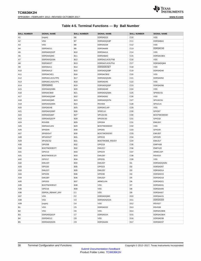
38
TCI6636K2HSPRS835H –FEBRUARY 2012–REVISED OCTOBER 2017 www.ti.com
Submit Documentation FeedbackProduct Folder Links: TCI6636K2H
Terminal Configuration and Functions Copyright © 2012–2017, Texas Instruments Incorporated
Table 4-5. Terminal Functions — By Ball Number
BALL NUMBER SIGNAL NAME BALL NUMBER SIGNAL NAME BALL NUMBER SIGNAL NAME
A1 (nopin) B6 DDR3AD23 C10 VSS
A2 VSS B7 DDR3ADQS3P C11 DDR3ABA1
A3 VSS B8 DDR3AD28 C12 VSS
A4 DDR3AD11 B9 DDR3AA08 C13 DDR3ACAS
A5 DDR3ADQS2P B10 DDR3AA14 C14 VSS
A6 DDR3ADQM2 B11 DDR3ABA0 C15 DDR3ACB01
A7 DDR3ADQS3N B12 DDR3ACLKOUTN0 C16 VSS
A8 DDR3AD27 B13 DDR3ACLKOUTN1 C17 DDR3ADQM4
A9 DDR3AA11 B14 DDR3ARESET C18 VSS
A10 DDR3AA13 B15 DDR3ADQS8P C19 DDR3AD40
A11 DDR3ACKE1 B16 DDR3ACB02 C20 VSS
A12 DDR3ACLKOUTP0 B17 DDR3ADQS4N C21 DDR3AD52
A13 DDR3ACLKOUTP1 B18 DDR3AD45 C22 VSS
A14 DDR3ARAS B19 DDR3ADQS5P C23 DDR3AD56
A15 DDR3ADQS8N B20 DDR3AD49 C24 VSS
A16 DDR3ACB00 B21 DDR3ADQS6N C25 SPI0SCS1
A17 DDR3ADQS4P B22 DDR3AD61 C26 VSS
A18 DDR3ADQM5 B23 DDR3ADQS7N C27 SPI1SCS1
A19 DDR3ADQS5N B24 RSV004 C28 SPI1CLK
A20 DDR3AD48 B25 DDR3ACLKP C29 VSS
A21 DDR3ADQS6P B26 SPI0CLK C30 GPIO07
A22 DDR3ADQM7 B27 SPI1SCS0 C30 BOOTMODE06†
A23 DDR3ADQS7P B28 SPI2SCS0 C31 GPIO18
A24 RSV005 B29 GPIO04 C31 EMU20†
A25 DDR3ACLKN B29 BOOTMODE03† C32 VSS
A26 SPI0DIN B30 GPIO01 C33 GPIO28
A27 SPI0DOUT B30 BOOTMODE00† C33 EMU30†
A28 SPI1DOUT B31 GPIO15 C34 GPIO29
A29 SPI2SCS2 B31 BOOTMODE_RSVD† C34 EMU31†
A30 GPIO08 B32 GPIO19 C35 EMIFA08
A30 BOOTMODE07† B32 EMU21† C36 EMIFA20
A31 GPIO13 B33 GPIO24 C37 ARMCLKP
A31 BOOTMODE12† B33 EMU26† C38 RSV010
A32 GPIO17 B34 GPIO31 C39 VSS
A32 EMU19† B34 EMU33† D1 DDR3ADQS0N
A33 GPIO20 B35 GPIO23 D2 DDR3AD07
A33 EMU22† B35 EMU25† D3 DDR3AD14
A34 GPIO26 B36 GPIO30 D4 DDR3AD15
A34 EMU28† B36 EMU32† D5 DDR3AD18
A35 GPIO03 B37 ARMCLKN D6 DDR3AD21
A35 BOOTMODE02† B38 VSS D7 DDR3AD31
A36 GPIO16 B39 VSS D8 DDR3AA09
A36 DDR3A_REMAP_EN† C1 VSS D9 DDR3AA07
A37 VSS C2 DDR3ADQM0 D10 DDR3AA15
A38 VSS C3 DDR3ADQS1N D11 DDR3ACE0
A39 (nopin) C4 VSS D12 RSV027
B1 VSS C5 DDR3AD22 D13 RSV028
B2 VSS C6 VSS D14 DDR3ACB06
B3 DDR3ADQS1P C7 DDR3AD24 D15 DDR3ACB04
B4 DDR3AD12 C8 VSS D16 DDR3AD36
B5 DDR3ADQS2N C9 DDR3AA06 D17 DDR3AD37

39
TCI6636K2Hwww.ti.com SPRS835H –FEBRUARY 2012–REVISED OCTOBER 2017
Submit Documentation FeedbackProduct Folder Links: TCI6636K2H
Terminal Configuration and FunctionsCopyright © 2012–2017, Texas Instruments Incorporated
Table 4-5. Terminal Functions — By Ball Number (continued)BALL NUMBER SIGNAL NAME BALL NUMBER SIGNAL NAME BALL NUMBER SIGNAL NAME
D18 DDR3AD46 E25 SPI2SCS3 F31 BOOTMODE09†
D19 DDR3AD41 E26 SPI0SCS2 F32 RSV016
D20 DDR3AD50 E27 SPI1SCS3 F33 EMIFRNW
D21 DDR3ADQM6 E28 VSS F34 EMIFA00
D22 DDR3AD63 E29 GPIO05 F35 EMIFA17
D23 DDR3AD58 E29 BOOTMODE04† F36 EMIFWE
D24 CORESEL2 E30 GPIO11 F37 EMIFA01
D25 SPI2CLK E30 BOOTMODE10† F38 EMIFA10
D26 SPI0SCS3 E31 GPIO25 F39 EMIFA15
D27 SPI1SCS2 E31 EMU27† G1 DDR3AD00
D28 SPI2SCS1 E32 GPIO14 G2 DDR3AD03
D29 GPIO02 E32 MAINPLLODSEL† G3 DDR3AD10
D29 BOOTMODE01† E33 RSV015 G4 DDR3AD16
D30 GPIO06 E34 EMIFA04 G5 DDR3AD20
D30 BOOTMODE05† E35 EMIFA13 G6 DDR3AD29
D31 GPIO22 E36 EMIFCE3 G7 DDR3AD30
D31 EMU24† E37 EMIFOE G8 DDR3AA02
D32 GPIO27 E38 EMIFWAIT0 G9 DDR3AA01
D32 EMU29† E39 EMIFA03 G10 DDR3AA03
D33 GPIO21 F1 DDR3AD02 G11 DDR3ABA2
D33 EMU23† F2 DDR3AD06 G12 DDR3ACKE0
D34 VSS F3 DDR3ADQM1 G13 DDR3AODT1
D35 EMIFA11 F4 DDR3AD09 G14 DDR3AVREFSSTL
D36 EMIFA23 F5 DDR3AD19 G15 DDR3ACB07
D37 VSS F6 DDR3AD26 G16 DDR3AD33
D38 RSV011 F7 DDR3AD25 G17 DDR3AD35
D39 EMIFWAIT1 F8 DDR3AA05 G18 DDR3AD42
E1 DDR3ADQS0P F9 DDR3AA04 G19 DDR3AD44
E2 DDR3AD05 F10 DDR3AA10 G20 DDR3AD51
E3 VSS F11 DDR3ACE1 G21 DDR3AD55
E4 DDR3AD08 F12 DDR3AWE G22 DDR3AD57
E5 VSS F13 RSV029 G23 VSS
E6 DDR3ADQM3 F14 DDR3ACB05 G24 CORESEL3
E7 VSS F15 DDR3ACB03 G24 ARMAVSSHARED†
E8 DDR3AA00 F16 DDR3AD34 G25 VSS
E9 VSS F17 DDR3AD38 G26 RSV018
E10 DDR3AA12 F18 DDR3AD47 G27 VSS
E11 VSS F19 DDR3AD43 G28 SPI2DOUT
E12 DDR3AODT0 F20 DDR3AD54 G29 VSS
E13 VSS F21 DDR3AD62 G30 GPIO09
E14 DDR3ADQM8 F22 DDR3AD59 G30 BOOTMODE08†
E15 VSS F23 RSV013 G31 VSS
E16 DDR3AD32 F24 CORESEL0 G32 EMIFCE1
E17 VSS F25 SPI0SCS0 G33 EMIFCE0
E18 DDR3AD39 F26 RSV017 G34 EMIFCE2
E19 VSS F27 SPI1DIN G35 VSS
E20 DDR3AD53 F28 SPI2DIN G36 EMIFA02
E21 VSS F29 GPIO00 G37 EMIFA09
E22 DDR3AD60 F30 GPIO12 G38 EMIFA14
E23 RSV014 F30 BOOTMODE11† G39 EMIFA19
E24 CORESEL1 F31 GPIO10 H1 DDR3AD04

40
TCI6636K2HSPRS835H –FEBRUARY 2012–REVISED OCTOBER 2017 www.ti.com
Submit Documentation FeedbackProduct Folder Links: TCI6636K2H
Terminal Configuration and Functions Copyright © 2012–2017, Texas Instruments Incorporated
Table 4-5. Terminal Functions — By Ball Number (continued)BALL NUMBER SIGNAL NAME BALL NUMBER SIGNAL NAME BALL NUMBER SIGNAL NAME
H2 DDR3AD01 J13 VSS K24 VSS
H3 DDR3AD13 J14 DVDD15 K25 DVDD18
H4 VSS J15 VSS K26 VSS
H5 DDR3AD17 J16 DVDD15 K27 DVDD18
H6 VSS J17 VSS K28 VSS
H7 DVDD15 J18 DVDD15 K29 CVDD
H8 VSS J19 VSS K30 VSS
H9 DVDD15 J20 DVDD15 K31 DVDD18
H10 DDR3ARZQ1 J21 VSS K32 VSS
H11 DVDD15 J22 DVDD15 K33 EMIFA07
H12 VSS J23 VSS K34 EMIFA16
H13 DVDD15 J24 VSS K35 VSS
H14 VSS J25 VSS K36 EMIFD10
H15 DVDD15 J26 DVDD18 K37 EMIFD06
H16 DDR3ARZQ0 J27 VSS K38 EMIFD09
H17 DVDD15 J28 DVDD18 K39 EMIFD08
H18 VSS J29 VSS L1 UART0CTS
H19 DVDD15 J30 CVDD L2 UART1RXD
H20 VSS J31 VSS L3 USBDRVVBUS
H21 DVDD15 J32 DVDD18 L4 UART0RTS
H22 DDR3ARZQ2 J33 VSS L5 VSS
H23 DVDD15 J34 EMIFA05 L6 CVDD
H24 VSS J35 EMIFA18 L7 VSS
H25 DVDD18 J36 EMIFA21 L8 DVDD15
H26 VSS J37 EMIFD01 L9 VSS
H27 DVDD18 J38 EMIFD05 L10 DVDD15
H28 VSS J39 EMIFD07 L11 VSS
H29 VSS K1 UART1CTS L12 DVDD15
H30 VSS K2 UART0TXD L13 VSS
H31 CVDD K3 UART1TXD L14 DVDD15
H32 VSS K4 UART0RXD L15 VSS
H33 EMIFBE1 K5 VSS L16 DVDD15
H34 EMIFBE0 K6 VSS L17 VSS
H35 EMIFA06 K7 DVDD15 L18 DVDD15
H36 EMIFA12 K8 VSS L19 VSS
H37 VSS K9 DVDD15 L20 DVDD15
H38 EMIFA22 K10 VSS L21 VSS
H39 EMIFD04 K11 DVDD15 L22 VPP
J1 VSS K12 VSS L23 VSS
J2 VSS K13 DVDD15 L24 DVDD18
J3 VSS K14 VSS L25 VSS
J4 VSS K15 DVDD15 L26 DVDD18
J5 VSS K16 VSS L27 VSS
J6 DVDD15 K17 DVDD15 L28 CVDD
J7 VSS K18 VSS L29 VSS
J8 DVDD15 K19 DVDD15 L30 DVDD18
J9 VSS K20 VSS L31 VSS
J10 DVDD15 K21 DVDD15 L32 DVDD15
J11 VSS K22 VSS L33 EMIFD02
J12 DVDD15 K23 DVDD15 L34 EMIFD03
L35 EMIFD12 N6 CVDD P18 VSS
L36 EMIFD11 N7 VSS P19 CVDD
L37 VSS N8 CVDD P20 VSS
L38 DDR3BD00 N9 VSS P21 CVDD
L39 DDR3BD03 N10 CVDD P22 VSS
M1 TIMI1 N11 VSS P23 CVDD
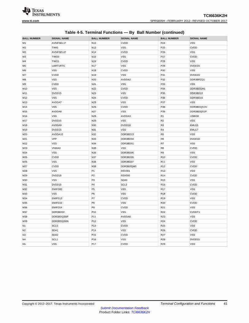
41
TCI6636K2Hwww.ti.com SPRS835H –FEBRUARY 2012–REVISED OCTOBER 2017
Submit Documentation FeedbackProduct Folder Links: TCI6636K2H
Terminal Configuration and FunctionsCopyright © 2012–2017, Texas Instruments Incorporated
Table 4-5. Terminal Functions — By Ball Number (continued)BALL NUMBER SIGNAL NAME BALL NUMBER SIGNAL NAME BALL NUMBER SIGNAL NAME
M1 AVSIFSEL1† N12 CVDD P24 VSS
M2 TIMI0 N13 VSS P25 CVDD
M2 AVSIFSEL0† N14 CVDD P26 VSS
M3 TIMO0 N15 VSS P27 CVDD
M4 TIMO1 N16 CVDD P28 VSS
M5 UART1RTS N17 VSS P29 DVDD15
M6 VSS N18 CVDD P30 VSS
M7 CVDD N19 VSS P31 DVDD15
M8 VSS N20 AVDDA2 P32 DDR3BRZQ1
M9 CVDD N21 VSS P33 VSS
M10 VSS N22 CVDD P34 DDR3BDQM1
M11 DVDD15 N23 VSS P35 DDR3BD10
M12 VSS N24 CVDD P36 DDR3BD15
M13 AVDDA7 N25 VSS P37 VSS
M14 VSS N26 CVDD P38 DDR3BDQS1N
M15 AVDDA8 N27 VSS P39 DDR3BDQS1P
M16 VSS N28 AVDDA3 R1 USBID0
M17 DVDD15 N29 VSS R2 VSS
M18 AVDDA9 N30 DVDD18 R3 EMU15
M19 DVDD15 N31 VSS R4 EMU17
M20 AVDDA10 N32 DDR3BD13 R5 VSS
M21 VPP N33 DDR3BD04 R6 DVDD18
M22 VSS N34 DDR3BD01 R7 VSS
M23 VNWA3 N35 VSS R8 CVDD
M24 VSS N36 DDR3BD06 R9 VSS
M25 CVDD N37 DDR3BD05 R10 CVDD
M26 VSS N38 DDR3BD07 R11 VSS
M27 CVDD N39 DDR3BDQM0 R12 CVDD
M28 VSS P1 RSV001 R13 VSS
M29 DVDD18 P2 RSV000 R14 CVDD
M30 VSS P3 SDA0 R15 VSS
M31 DVDD15 P4 SCL2 R16 CVDD
M32 EMIFD00 P5 VSS R17 VSS
M33 VSS P6 VSS R18 CVDD
M34 EMIFD13 P7 CVDD R19 VSS
M35 EMIFD15 P8 VSS R20 CVDD
M36 EMIFD14 P9 CVDD R21 VSS
M37 DDR3BD02 P10 VSS R22 CVDDT1
M38 DDR3BDQS0P P11 AVDDA6 R23 VSS
M39 DDR3BDQS0N P12 VSS R24 CVDD
N1 SCL0 P13 CVDD R25 VSS
N2 SDA1 P14 VSS R26 CVDD
N3 SDA2 P15 CVDD R27 VSS
N4 SCL1 P16 VSS R28 DVDD15
N5 VSS P17 CVDD R29 VSS

42
TCI6636K2HSPRS835H –FEBRUARY 2012–REVISED OCTOBER 2017 www.ti.com
Submit Documentation FeedbackProduct Folder Links: TCI6636K2H
Terminal Configuration and Functions Copyright © 2012–2017, Texas Instruments Incorporated
Table 4-5. Terminal Functions — By Ball Number (continued)BALL NUMBER SIGNAL NAME BALL NUMBER SIGNAL NAME BALL NUMBER SIGNAL NAME
R30 DVDD15 U3 EMU08 V15 CVDD
R31 VSS U4 EMU07 V16 VSS
R32 DDR3BD09 U5 EMU12 V17 CVDD1
R33 DDR3BD14 U6 DVDD18 V18 VSS
R34 DDR3BD17 U7 VSS V19 CVDD
R35 VSS U8 CVDD V20 VSS
R36 DDR3BD20 U9 VSS V21 CVDD1
R37 DDR3BD19 U10 CVDD V22 VSS
R38 DDR3BD12 U11 VSS V23 CVDD
R39 DDR3BD11 U12 CVDD V24 VSS
T1 USBVBUS U13 VSS V25 CVDD
T2 USBDM U14 CVDD1 V26 VSS
T3 EMU09 U15 VSS V27 CVDD
T4 EMU13 U16 CVDD1 V28 VSS
T5 EMU16 U17 VSS V29 DVDD15
T6 VSS U18 CVDD V30 VSS
T7 DVDD18 U19 VSS V31 DVDD15
T8 VSS U20 CVDD1 V32 DDR3BD30
T9 CVDD U21 VSS V33 VSS
T10 VSS U22 CVDDT1 V34 DDR3BA05
T11 CVDD U23 VSS V35 DDR3BD24
T12 VSS U24 CVDD V36 DDR3BD31
T13 CVDD1 U25 VSS V37 VSS
T14 VSS U26 CVDD V38 DDR3BDQS3N
T15 CVDD U27 VSS V39 DDR3BDQS3P
T16 VSS U28 DVDD15 W1 USBRX0P
T17 CVDD U29 VSS W2 USBCLKP
T18 VSS U30 DVDD15 W3 EMU04
T19 CVDD U31 VSS W4 EMU05
T20 VSS U32 DDR3BDQM3 W5 VSS
T21 CVDD1 U33 DDR3BD29 W6 DVDD18
T22 VSS U34 DDR3BD26 W7 VSS
T23 CVDD U35 VSS W8 CVDD
T24 VSS U36 DDR3BD25 W9 VSS
T25 CVDD U37 DDR3BD21 W10 CVDD
T26 VSS U38 DDR3BD23 W11 VSS
T27 CVDD U39 DDR3BDQM2 W12 CVDD
T28 VSS V1 USBTX0M W13 VSS
T29 DVDD15 V2 USBCLKM W14 CVDD
T30 VSS V3 VSS W15 VSS
T31 DVDD15 V4 EMU06 W16 CVDD1
T32 DDR3BD08 V5 DVDD18 W17 VSS
T33 VSS V6 VSS W18 CVDD
T34 DDR3BD16 V7 DVDD18 W19 VSS
T35 DDR3BD18 V8 VSS W20 CVDD
T36 DDR3BD22 V9 CVDD W21 VSS
T37 VSS V10 VSS W22 CVDDT1
T38 DDR3BDQS2N V11 VNWA4 W23 VSS
T39 DDR3BDQS2P V12 VSS W24 CVDD
U1 USBTX0P V13 CVDD1 W25 VSS
U2 USBDP V14 VSS W26 CVDD

43
TCI6636K2Hwww.ti.com SPRS835H –FEBRUARY 2012–REVISED OCTOBER 2017
Submit Documentation FeedbackProduct Folder Links: TCI6636K2H
Terminal Configuration and FunctionsCopyright © 2012–2017, Texas Instruments Incorporated
Table 4-5. Terminal Functions — By Ball Number (continued)BALL NUMBER SIGNAL NAME BALL NUMBER SIGNAL NAME BALL NUMBER SIGNAL NAME
W27 VSS Y39 DDR3BA13 AB12 VSS
W28 DVDD15 AA1 USBRESREF AB13 VDDUSB
W29 VSS AA2 EMU00 AB14 VSS
W30 DVDD15 AA3 EMU11 AB15 CVDD
W31 VSS AA4 EMU18 AB16 VSS
W32 DDR3BA02 AA5 VSS AB17 CVDD
W33 DDR3BA01 AA6 DVDD18 AB18 VSS
W34 DDR3BA04 AA7 VSS AB19 CVDD
W35 VSS AA8 CVDD AB20 VSS
W36 DDR3BA06 AA9 VSS AB21 CVDD
W37 DDR3BA07 AA10 CVDD AB22 VSS
W38 DDR3BD27 AA11 VSS AB23 CVDD
W39 DDR3BD28 AA12 VP AB24 VSS
Y1 USBRX0M AA13 VSS AB25 CVDD
Y2 VSS AA14 DVDD33 AB26 VSS
Y3 EMU02 AA15 VSS AB27 CVDD
Y4 EMU03 AA16 CVDD AB28 AVDDA12
Y5 DVDD18 AA17 VSS AB29 DVDD15
Y6 VSS AA18 CVDD AB30 VSS
Y7 DVDD18 AA19 VSS AB31 DVDD15
Y8 VSS AA20 CVDD AB32 RSV032
Y9 CVDD AA21 VSS AB33 VSS
Y10 VSS AA22 CVDD AB34 DDR3BCE0
Y11 VPTX AA23 VSS AB35 DDR3BBA2
Y12 VSS AA24 CVDD AB36 VSS
Y13 VPH AA25 VSS AB37 VSS
Y14 VSS AA26 CVDD AB38 DDR3BCKE1
Y15 CVDD AA27 VSS AB39 DDR3BCKE0
Y16 VSS AA28 DVDD15 AC1 TSPUSHEVT1
Y17 CVDD AA29 VSS AC2 TSPUSHEVT0
Y18 VSS AA30 DVDD15 AC3 TSSYNCEVT
Y19 CVDD AA31 DDR3BRZQ0 AC4 EXTFRAMEEVENT
Y20 VSS AA32 DDR3BA00 AC5 RESETSTAT
Y21 CVDD AA33 DDR3BA08 AC6 DVDD18
Y22 VSS AA34 DDR3BBA1 AC7 VSS
Y23 CVDD AA35 VSS AC8 CVDD
Y24 VSS AA36 DDR3BCE1 AC9 VSS
Y25 CVDD AA37 DDR3BBA0 AC10 CVDD
Y26 VSS AA38 DDR3BA14 AC11 VSS
Y27 CVDD AA39 DDR3BA11 AC12 CVDD
Y28 AVDDA11 AB1 TSCOMPOUT AC13 VSS
Y29 DVDD15 AB2 EMU01 AC14 CVDD
Y30 VSS AB3 EMU14 AC15 VSS
Y31 DVDD15 AB4 EMU10 AC16 CVDD
Y32 DDR3BA09 AB5 DVDD18 AC17 VSS
Y33 VSS AB6 VSS AC18 CVDD1
Y34 DDR3BA03 AB7 DVDD18 AC19 VSS
Y35 DDR3BA12 AB8 VSS AC20 CVDD
Y36 DDR3BA15 AB9 CVDD AC21 VSS
Y37 VSS AB10 VSS AC22 CVDD
Y38 DDR3BA10 AB11 CVDD AC23 VSS

44
TCI6636K2HSPRS835H –FEBRUARY 2012–REVISED OCTOBER 2017 www.ti.com
Submit Documentation FeedbackProduct Folder Links: TCI6636K2H
Terminal Configuration and Functions Copyright © 2012–2017, Texas Instruments Incorporated
Table 4-5. Terminal Functions — By Ball Number (continued)BALL NUMBER SIGNAL NAME BALL NUMBER SIGNAL NAME BALL NUMBER SIGNAL NAME
AC24 CVDD AD36 DDR3BCB06 AF9 CVDD
AC25 VSS AD37 VSS AF10 VSS
AC26 CVDD AD38 DDR3BCLKOUTP0 AF11 AVDDA1
AC27 VSS AD39 DDR3BCLKOUTN0 AF12 VSS
AC28 AVDDA13 AE1 TCK AF13 VDDALV
AC29 VSS AE2 TMS AF14 VSS
AC30 DVDD15 AE3 VSS AF15 VDDALV
AC31 DDR3BVREFSSTL AE4 LRESET AF16 VSS
AC32 DDR3BRESET AE5 HOUT AF17 VDDALV
AC33 DDR3BODT0 AE6 DVDD18 AF18 VSS
AC34 RSV031 AE7 VSS AF19 VDDALV
AC35 VSS AE8 CVDD AF20 VSS
AC36 DDR3BCAS AE9 VSS AF21 VDDALV
AC37 DDR3BWE AE10 CVDD AF22 VSS
AC38 DDR3BCLKOUTN1 AE11 VSS AF23 VDDALV
AC39 DDR3BCLKOUTP1 AE12 CVDD AF24 VSS
AD1 TRST AE13 VSS AF25 CVDD
AD2 RESET AE14 CVDD AF26 VSS
AD3 RESETFULL AE15 VSS AF27 CVDD
AD4 LRESETNMIEN AE16 CVDD AF28 VSS
AD5 NMI AE17 VSS AF29 DVDD15
AD6 VSS AE18 CVDD AF30 VSS
AD7 DVDD18 AE19 VSS AF31 DVDD15
AD8 VSS AE20 CVDD AF32 DDR3BCB00
AD9 CVDD AE21 VSS AF33 VSS
AD10 VSS AE22 CVDD AF34 DDR3BCB01
AD11 VNWA2 AE23 VSS AF35 DDR3BCB03
AD12 VSS AE24 CVDD AF36 DDR3BD33
AD13 CVDD AE25 VSS AF37 VSS
AD14 VSS AE26 CVDD AF38 DDR3BDQS4P
AD15 CVDD AE27 VSS AF39 DDR3BDQS4N
AD16 VSS AE28 AVDDA15 AG1 TDI
AD17 CVDD1 AE29 VSS AG2 HYP1RXFLDAT
AD18 VSS AE30 DVDD15 AG3 HYP0RXPMDAT
AD19 CVDD1 AE31 VSS AG4 VSS
AD20 VSS AE32 DDR3BCB02 AG5 HYP0TXFLDAT
AD21 CVDD AE33 DDR3BCB04 AG6 DVDD18
AD22 VSS AE34 DDR3BCB07 AG7 VSS
AD23 CVDD AE35 VSS AG8 CVDD
AD24 VSS AE36 DDR3BCB05 AG9 VSS
AD25 CVDD AE37 DDR3BDQM8 AG10 CVDD
AD26 VSS AE38 DDR3BDQS8N AG11 VSS
AD27 CVDD AE39 DDR3BDQS8P AG12 VDDALV
AD28 AVDDA14 AF1 TDO AG13 VSS
AD29 DVDD15 AF2 HYP1TXPMDAT AG14 VDDALV
AD30 VSS AF3 HYP1RXPMCLK AG15 VSS
AD31 DVDD15 AF4 HYP1RXPMDAT AG16 VDDALV
AD32 DDR3BRAS AF5 BOOTCOMPLETE AG17 VSS
AD33 VSS AF6 VSS AG18 VDDALV
AD34 DDR3BODT1 AF7 DVDD18 AG19 VSS
AD35 RSV030 AF8 VSS AG20 VDDALV

45
TCI6636K2Hwww.ti.com SPRS835H –FEBRUARY 2012–REVISED OCTOBER 2017
Submit Documentation FeedbackProduct Folder Links: TCI6636K2H
Terminal Configuration and FunctionsCopyright © 2012–2017, Texas Instruments Incorporated
Table 4-5. Terminal Functions — By Ball Number (continued)BALL NUMBER SIGNAL NAME BALL NUMBER SIGNAL NAME BALL NUMBER SIGNAL NAME
AG21 VSS AH33 VSS AK6 VSS
AG22 VDDALV AH34 DDR3BD37 AK7 CVDD
AG23 VSS AH35 DDR3BD38 AK8 VSS
AG24 VNWA1 AH36 DDR3BD42 AK9 CVDD
AG25 VSS AH37 VSS AK10 VSS
AG26 AVDDA5 AH38 DDR3BD46 AK11 VDDAHV
AG27 VSS AH39 DDR3BD45 AK12 VSS
AG28 CVDD AJ1 HYP0TXPMDAT AK13 VDDAHV
AG29 VSS AJ2 HYP0RXPMCLK AK14 VSS
AG30 DVDD15 AJ3 HYP0TXFLCLK AK15 VDDAHV
AG31 VSS AJ4 HYP0RXFLDAT AK16 VSS
AG32 DDR3BD39 AJ5 HYP0RXFLCLK AK17 VDDAHV
AG33 DDR3BDQM4 AJ6 VSS AK18 VSS
AG34 DDR3BD35 AJ7 VSS AK19 VDDAHV
AG35 VSS AJ8 CVDD AK20 VSS
AG36 DDR3BD36 AJ9 VSS AK21 VDDAHV
AG37 DDR3BD32 AJ10 CVDD AK22 VSS
AG38 DDR3BD34 AJ11 VSS AK23 VDDAHV
AG39 DDR3BDQM5 AJ12 VDDALV AK24 VSS
AH1 HYP1TXPMCLK AJ13 VSS AK25 VDDAHV
AH2 HYP1TXFLDAT AJ14 VDDALV AK26 VSS
AH3 HYP1TXFLCLK AJ15 VSS AK27 DVDD18
AH4 HYP1RXFLCLK AJ16 VDDALV AK28 VSS
AH5 HYP0TXPMCLK AJ17 VSS AK29 CVDD
AH6 VSS AJ18 VDDALV AK30 VSS
AH7 VSS AJ19 VSS AK31 DVDD15
AH8 VSS AJ20 VDDALV AK32 DDR3BRZQ2
AH9 CVDD AJ21 VSS AK33 VSS
AH10 VSS AJ22 VDDALV AK34 DDR3BDQM6
AH11 VDDALV AJ23 VSS AK35 DDR3BD51
AH12 VSS AJ24 VDDALV AK36 DDR3BD50
AH13 VDDALV AJ25 VSS AK37 VSS
AH14 VSS AJ26 DVDD18 AK38 DDR3BD49
AH15 VDDALV AJ27 VSS AK39 DDR3BD48
AH16 VSS AJ28 CVDD AL1 TSREFCLKN
AH17 VDDALV AJ29 VSS AL2 ALTCORECLKN
AH18 VSS AJ30 DVDD15 AL3 SYSCLKP
AH19 VDDALV AJ31 VSS AL4 CORECLKSEL
AH20 VSS AJ32 VSS AL5 VSS
AH21 VDDALV AJ33 DDR3BD41 AL6 CVDD
AH22 VSS AJ34 DDR3BD43 AL7 VSS
AH23 VDDALV AJ35 VSS AL8 CVDD
AH24 VSS AJ36 DDR3BD44 AL9 VSS
AH25 VDDALV AJ37 DDR3BD47 AL10 VDDAHV
AH26 VSS AJ38 DDR3BDQS5N AL11 VSS
AH27 CVDD AJ39 DDR3BDQS5P AL12 VDDAHV
AH28 VSS AK1 SYSCLKOUT AL13 VSS
AH29 AVDDA4 AK2 VSS AL14 VDDAHV
AH30 VSS AK3 SYSCLKN AL15 VSS
AH31 DVDD15 AK4 POR AL16 VDDAHV
AH32 DDR3BD40 AK5 RSV012 AL17 VSS

46
TCI6636K2HSPRS835H –FEBRUARY 2012–REVISED OCTOBER 2017 www.ti.com
Submit Documentation FeedbackProduct Folder Links: TCI6636K2H
Terminal Configuration and Functions Copyright © 2012–2017, Texas Instruments Incorporated
Table 4-5. Terminal Functions — By Ball Number (continued)BALL NUMBER SIGNAL NAME BALL NUMBER SIGNAL NAME BALL NUMBER SIGNAL NAME
AL18 VDDAHV AM30 RADSYNC AP3 TSRXCLKOUT1N
AL19 VSS AM31 CVDD AP4 VSS
AL20 VDDAHV AM32 VSS AP5 HYP1TXN1
AL21 VSS AM33 VSS AP6 HYP1TXP1
AL22 VDDAHV AM34 DDR3BD59 AP7 VSS
AL23 VSS AM35 DDR3BD60 AP8 HYP0TXN2
AL24 VDDAHV AM36 DDR3BD62 AP9 HYP0TXP2
AL25 VSS AM37 VSS AP10 VSS
AL26 DVDD18 AM38 DDR3BD61 AP11 HYP0TXN0
AL27 VSS AM39 DDR3BDQM7 AP12 HYP0TXP0
AL28 DVDD18 AN1 TSRXCLKOUT0P AP13 VSS
AL29 VSS AN2 VSS AP14 AIFTXN3
AL30 CVDD AN3 TSRXCLKOUT1P AP15 AIFTXP3
AL31 VSS AN4 RSV002 AP16 VSS
AL32 DVDD15 AN5 VSS AP17 AIFTXN0
AL33 DDR3BD55 AN6 VSS AP18 AIFTXP0
AL34 DDR3BD52 AN7 VSS AP19 VSS
AL35 VSS AN8 VSS AP20 VSS
AL36 DDR3BD53 AN9 VSS AP21 VSS
AL37 DDR3BD54 AN10 RSV019 AP22 RIOTXN2
AL38 DDR3BDQS6N AN11 VSS AP23 RIOTXP2
AL39 DDR3BDQS6P AN12 VSS AP24 VSS
AM1 TSREFCLKP AN13 VSS AP25 SGMII3TXN
AM2 ALTCORECLKP AN14 VSS AP26 SGMII3TXP
AM3 VSS AN15 VSS AP27 VSS
AM4 RSV003 AN16 RSV068 AP28 VSS
AM5 CVDD AN17 VSS AP29 VSS
AM6 HYP1REFRES AN18 VSS AP30 VSS
AM7 RSV020 AN19 RSV026 AP31 MDCLK
AM8 VSS AN20 VSS AP32 USIMRST
AM9 HYP0REFRES AN21 VSS AP33 USIMIO
AM10 VSS AN22 VSS AP34 PHYSYNC
AM11 AIFREFRES1 AN23 VSS AP35 VD
AM12 VSS AN24 VSS AP36 VCL
AM13 VSS AN25 VSS AP37 VSS
AM14 RSV025 AN26 VSS AP38 RSV006
AM15 AIFREFRES0 AN27 VSS AP39 RSV007
AM16 RSV024 AN28 VSS AR1 RP1FBP
AM17 VSS AN29 VSS AR2 RP1CLKP
AM18 VSS AN30 PACLKSEL AR3 VSS
AM19 RSV069 AN31 VSS AR4 HYP1TXN2
AM20 VSS AN32 USIMCLK AR5 HYP1TXP2
AM21 RIOREFRES AN33 DDR3BD58 AR6 VSS
AM22 VSS AN34 DDR3BD56 AR7 HYP0TXN3
AM23 RSV021 AN35 VSS AR8 HYP0TXP3
AM24 SGMIIREFRES AN36 DDR3BD57 AR9 VSS
AM25 RSV023 AN37 DDR3BD63 AR10 HYP0TXN1
AM26 PCIEREFRES AN38 DDR3BDQS7P AR11 HYP0TXP1
AM27 DVDD18 AN39 DDR3BDQS7N AR12 VSS
AM28 RSV022 AP1 TSRXCLKOUT0N AR13 AIFTXN4
AM29 DVDD18 AP2 RP1CLKN AR14 AIFTXP4
47
TCI6636K2Hwww.ti.com SPRS835H –FEBRUARY 2012–REVISED OCTOBER 2017
Submit Documentation FeedbackProduct Folder Links: TCI6636K2H
Terminal Configuration and FunctionsCopyright © 2012–2017, Texas Instruments Incorporated
Table 4-5. Terminal Functions — By Ball Number (continued)BALL NUMBER SIGNAL NAME BALL NUMBER SIGNAL NAME BALL NUMBER SIGNAL NAME
AR15 VSS AT27 SGMII1TXN AU39 VSS
AR16 AIFTXN1 AT28 SGMII1TXP AV1 VSS
AR17 AIFTXP1 AT29 VSS AV2 VSS
AR18 VSS AT30 PCIETXN0 AV3 HYP1RXN3
AR19 RSV067 AT31 PCIETXP0 AV4 HYP1RXP3
AR20 RSV066 AT32 VSS AV5 VSS
AR21 VSS AT33 RSV072 AV6 HYP1RXN1
AR22 VSS AT34 RSV009 AV7 HYP1RXP1
AR23 RIOTXN1 AT35 RSV075 AV8 VSS
AR24 RIOTXP1 AT36 VSS AV9 HYP0RXN2
AR25 VSS AT37 RSV074 AV10 HYP0RXP2
AR26 SGMII2TXN AT38 VCNTL3 AV11 VSS
AR27 SGMII2TXP AT39 VCNTL0 AV12 AIFRXN5
AR28 VSS AU1 VSS AV13 AIFRXP5
AR29 PCIETXN1 AU2 VSS AV14 VSS
AR30 PCIETXP1 AU3 VSS AV15 AIFRXN2
AR31 VSS AU4 HYP1RXN2 AV16 AIFRXP2
AR32 MDIO AU5 HYP1RXP2 AV17 VSS
AR33 VSS AU6 VSS AV18 RSV061
AR34 RSV073 AU7 HYP1RXN0 AV19 RSV060
AR35 VCNTL5 AU8 HYP1RXP0 AV20 VSS
AR36 VCNTL2 AU9 VSS AV21 RIORXN3
AR37 VCNTL1 AU10 HYP0RXN1 AV22 RIORXP3
AR38 DDR3BCLKP AU11 HYP0RXP1 AV23 VSS
AR39 DDR3BCLKN AU12 VSS AV24 RIORXN0
AT1 RP1FBN AU13 AIFRXN4 AV25 RIORXP0
AT2 VSS AU14 AIFRXP4 AV26 VSS
AT3 HYP1TXN3 AU15 VSS AV27 SGMII1RXN
AT4 HYP1TXP3 AU16 AIFRXN1 AV28 SGMII1RXP
AT5 VSS AU17 AIFRXP1 AV29 VSS
AT6 HYP1TXN0 AU18 VSS AV30 PCIERXN1
AT7 HYP1TXP0 AU19 RSV070 AV31 PCIERXP1
AT8 VSS AU20 RSV071 AV32 VSS
AT9 HYP0CLKP AU21 VSS AV33 PASSCLKP
AT10 HYP0CLKN AU22 RIORXN1 AV34 PASSCLKN
AT11 VSS AU23 RIORXP1 AV35 VSS
AT12 AIFTXN5 AU24 VSS AV36 RSV079
AT13 AIFTXP5 AU25 SGMII2RXN AV37 RSV077
AT14 VSS AU26 SGMII2RXP AV38 VSS
AT15 AIFTXN2 AU27 VSS AV39 VSS
AT16 AIFTXP2 AU28 SGMII0TXN AW1 (nopin)
AT17 VSS AU29 SGMII0TXP AW2 VSS
AT18 RSV063 AU30 VSS AW3 VSS
AT19 RSV062 AU31 PCIERXN0 AW4 HYP1CLKP
AT20 VSS AU32 PCIERXP0 AW5 HYP1CLKN
AT21 RIOTXN3 AU33 VSS AW6 VSS
AT22 RIOTXP3 AU34 RSV008 AW7 HYP0RXN3
AT23 VSS AU35 RSV080 AW8 HYP0RXP3
AT24 RIOTXN0 AU36 RSV076 AW9 VSS
AT25 RIOTXP0 AU37 RSV078 AW10 HYP0RXN0
AT26 VSS AU38 VCNTL4 AW11 HYP0RXP0

48
TCI6636K2HSPRS835H –FEBRUARY 2012–REVISED OCTOBER 2017 www.ti.com
Submit Documentation FeedbackProduct Folder Links: TCI6636K2H
Terminal Configuration and Functions Copyright © 2012–2017, Texas Instruments Incorporated
Table 4-5. Terminal Functions — By Ball Number (continued)BALL NUMBER SIGNAL NAME BALL NUMBER SIGNAL NAME BALL NUMBER SIGNAL NAME
AW12 VSS AW22 RIORXN2 AW31 PCIECLKP
AW13 AIFRXN3 AW23 RIORXP2 AW32 PCIECLKN
AW14 AIFRXP3 AW24 VSS AW33 VSS
AW15 VSS AW25 SGMII3RXN AW34 SRIOSGMIICLKP
AW16 AIFRXN0 AW26 SGMII3RXP AW35 SRIOSGMIICLKN
AW17 AIFRXP0 AW27 VSS AW36 RSV081
AW18 VSS AW28 SGMII0RXN AW37 VSS
AW19 RSV065 AW29 SGMII0RXP AW38 VSS
AW20 RSV064 AW30 VSS AW39 (nopin)
AW21 VSS
4.4 Pullup/Pulldown ResistorsProper board design should ensure that input pins to the device always be at a valid logic level and notfloating. This may be achieved via pullup/pulldown resistors. The device features internal pullup (IPU) andinternal pulldown (IPD) resistors on most pins to eliminate the need, unless otherwise noted, for externalpullup/pulldown resistors.
An external pullup/pulldown resistor needs to be used in the following situations:• Device Configuration Pins: If the pin is both routed out and not driven (in Hi-Z state), an external
pullup/pulldown resistor must be used, even if the IPU/IPD matches the desired value/state.• Other Input Pins: If the IPU/IPD does not match the desired value/state, use an external
pullup/pulldown resistor to pull the signal to the opposite rail.
For the device configuration pins (listed in Table 10-29), if they are both routed out and are not driven (inHi-Z state), it is strongly recommended that an external pullup/pulldown resistor be implemented.Although, internal pullup/pulldown resistors exist on these pins and they may match the desiredconfiguration value, providing external connectivity can help ensure that valid logic levels are latched onthese device configuration pins. In addition, applying external pullup/pulldown resistors on the deviceconfiguration pins adds convenience to the user in debugging and flexibility in switching operating modes.
Tips for choosing an external pullup/pulldown resistor:• Consider the total amount of current that may pass through the pullup or pulldown resistor. Be sure to
include the leakage currents of all the devices connected to the net, as well as any internal pullup orpulldown resistors.
• Decide a target value for the net. For a pulldown resistor, this should be below the lowest VIL level ofall inputs connected to the net. For a pullup resistor, this should be above the highest VIH level of allinputs on the net. A reasonable choice would be to target the VOL or VOH levels for the logic family ofthe limiting device; which, by definition, have margin to the VIL and VIH levels.
• Select a pullup/pulldown resistor with the largest possible value that still ensures that the net will reachthe target pulled value when maximum current from all devices on the net is flowing through theresistor. The current to be considered includes leakage current plus, any other internal and externalpullup/pulldown resistors on the net.
• For bidirectional nets, there is an additional consideration that sets a lower limit on the resistance valueof the external resistor. Verify that the resistance is small enough that the weakest output buffer candrive the net to the opposite logic level (including margin).
• Remember to include tolerances when selecting the resistor value.• For pullup resistors, also remember to include tolerances on the DVDD rail.
For most systems:• A 1-kΩ resistor can be used to oppose the IPU/IPD while meeting the above criteria. Users should
confirm this resistor value is correct for their specific application.

49
TCI6636K2Hwww.ti.com SPRS835H –FEBRUARY 2012–REVISED OCTOBER 2017
Submit Documentation FeedbackProduct Folder Links: TCI6636K2H
Terminal Configuration and FunctionsCopyright © 2012–2017, Texas Instruments Incorporated
• A 20-kΩ resistor can be used to compliment the IPU/IPD on the device configuration pins whilemeeting the above criteria. Users should confirm this resistor value is correct for their specificapplication.
For more detailed information on input current (II), and the low-level and high-level input voltages (VIL andVIH) for the TCI6636K2H device, see Section 5.5. To determine which pins on the device include internalpullup/pulldown resistors, see Table 4-3.

50
TCI6636K2HSPRS835H –FEBRUARY 2012–REVISED OCTOBER 2017 www.ti.com
Submit Documentation FeedbackProduct Folder Links: TCI6636K2H
Specifications Copyright © 2012–2017, Texas Instruments Incorporated
(1) Stresses beyond those listed under Absolute Maximum Ratings may cause permanent damage to the device. These are stress ratingsonly, and functional operation of the device at these or any other conditions beyond those indicated under Recommended OperatingConditions is not implied. Exposure to absolute-maximum-rated conditions for extended periods may affect device reliability.
(2) All voltage values are with respect to VSS.(3) For USB High-Speed, Full-Speed, and Low -Speed modes, USB I/Os adhere to Universal Serial Bus, revision 2.0 standard. For USB
Super-Speed mode, USB I/Os adhere to Universal Serial Bus, revision 3.1 specification, revision 1.0 standard.(4) Overshoot/Undershoot percentage relative to I/O operating values - for example the maximum overshoot value for 1.8 V LVCMOS
signals is DVDD18 + 0.20 × DVDD18 and maximum undershoot value would be VSS - 0.20 × DVDD18
5 Specifications
5.1 Absolute Maximum Ratingsover operating case temperature range (unless otherwise noted) (1)
Supply voltage (2):
CVDD –0.3 V to 1.3 VCVDD1 –0.3 V to 1.3 VCVDDT1 –0.3 V to 1.3 VDVDD15 –0.3 V to 1.98 VDVDD18 –0.3 V to 2.45 VDVDD33 –0.3V to 3.63 VDDR3VREFSSTL 0.49 × DVDD15 to 0.51 × DVDD15VDDAHV –0.3 V to 1.98 VVDDALV –0.3 V to 0.935 VVDDUSB –0.3V to 0.935 VAVDDA1, AVDDA2, AVDDA3,AVDDA4,AVDDA5 –0.3 V to 1.98 V
AVDDA6, AVDDA7, AVDDA8, AVDDA9,AVDDA10, AVDDA11, AVDDA12,AVDDA13, AVDDA14, AVDDA15
–0.3 V to 1.98 V
VSS Ground 0 V
Input voltage (VI): (3)
LVCMOS (1.8 V) –0.3 V to DVDD18+0.3 VDDR3A, DDR3B –0.3 V to 1.98 VI2C –0.3 V to 2.45 VLVDS –0.3 V to DVDD18+0.3 VLJCB –0.3 V to 1.3 VSerDes –0.3 V to VDDAHV1+0.3 V
Output voltage (VO):(3)
LVCMOS (1.8 V) –0.3 V to DVDD18+0.3 VDDR3A, DDR3B –0.3 V to 1.98 VI2C –0.3 V to 2.45 VSerDes –0.3 V to VDDAHV+0.3 V
Operating case temperature, TC:Commercial 0°C to 85°CExtended –40°C to 100°C
Overshoot/undershoot (4)
LVCMOS (1.8 V)20% overshoot/undershoot for 20% of
signal duty cycleDDR3A, DDR3BI2C
Storage temperature, Tstg: –65°C to 150°C
(1) JEDEC document JEP155 states that 500-V HBM allows safe manufacturing with a standard ESD control process.(2) JEDEC document JEP157 states that 250-V CDM allows safe manufacturing with a standard ESD control process.
5.2 ESD RatingsVALUE UNIT
VESDElectrostatic discharge(ESD)
Human body model (HBM), per ANSI/ESDA/JEDEC JS-001 (1) ±1000V
Charged device model (CDM), per JESD22-C101 (2) ±250

51
TCI6636K2Hwww.ti.com SPRS835H –FEBRUARY 2012–REVISED OCTOBER 2017
Submit Documentation FeedbackProduct Folder Links: TCI6636K2H
SpecificationsCopyright © 2012–2017, Texas Instruments Incorporated
(1) All differential clock inputs comply with the LVDS Electrical Specification, IEEE 1596.3-1996 and all SerDes I/Os comply with the XAUIElectrical Specification, IEEE 802.3ae-2002.
(2) All SerDes I/Os comply with the XAUI Electrical Specification, IEEE 802.3ae-2002.(3) Users are required to program their board CVDD supply initial value to 1.0 V on the device. The initial CVDD voltage at power-on will be
1.0 V nominal and it must transition to VID set value, immediately after being presented on the VCNTL pins. This is required to maintainfull power functionality and reliability targets ensured by TI.
(4) SRVnom refers to the unique SmartReflex core supply voltage that has a potential range of 0.8 V and 1.1 V which preset from thefactory for each individual device. Your device may never be programmed to operate at the upper range but has been designedaccordingly should it be determined to be acceptable or necessary. Power supplies intended to support the variable SRV function shallbe capable of providing a 0.8 V-1.1 V dynamic range using a 4- or 6-bit binary input value which as provided by the DSP SmartReflexoutput.
(5) Where x = 1,2,3,4... to indicate all supplies of the same kind.(6) For USB High-Speed, Full-Speed, and Low -Speed modes, USB I/Os adhere to Universal Serial Bus, revision 2.0 standard. For USB
Super-Speed mode, USB I/Os adhere to Universal Serial Bus, revision 3.1 specification, revision 1.0 standard.
5.3 Recommended Operating Conditions(1) (2)
MIN NOM MAX UNIT
CVDD SR DSP core supply
Initial (3) 0.95 1.0 1.05 V
1000-MHzdevice
SRVnom*0.95 (4) SRVnom SRVnom*1.05 V
1200-MHzdevice
SRVnom*0.95 (4) SRVnom SRVnom*1.05 V
CVDD1 DSP core supply 0.902 0.95 0.997 V
CVDDT1 Cortex-A15 processor core supply 0.902 0.95 0.997 V
DVDD18 1.8-V supply I/O voltage 1.71 1.8 1.89 V
DVDD15 DDR3 I/O voltage
DDR3 1.425 1.5 1.575
VDDR3L at 1.5 V 1.425 1.5 1.575
DDR3L at 1.35 V 1.283 1.35 1.45
DDR3VREFSSTL DDR3A, DDR3B reference voltage 0.49 × DVDD15 0.5 × DVDD15 0.51 × DVDD15 V
VDDAHV SerDes regulator supply 1.71 1.8 1.89 V
AVDDx (5) PLL analog, DDR DLL supply 1.71 1.8 1.89 V
VDDALH SerDes termination supply 0.807 0.85 0.892 V
DVDD33 USB 3.135 3.3 3.465 V
VDDUSB USB 0.807 0.85 0.892 V
VSS Ground 0 0 0 V
VIH(6) High-level input voltage
LVCMOS (1.8 V) 0.65 × DVDD18
VI2C 0.7 × DVDD18
DDR3A, DDR3B EMIF VREFSSTL + 0.1
VIL(6) Low-level input voltage
LVCMOS (1.8 V) 0.35 × DVDD18
VDDR3A, DDR3B EMIF -0.3 VREFSSTL - 0.1
I2C 0.3 × DVDD18
TC Operating case temperatureCommercial 0 100
°CExtended –40 100
5.4 Power Consumption SummaryFor information on the device power consumption, see Power Consumption Summary for KeyStoneTCI66x Devices.

52
TCI6636K2HSPRS835H –FEBRUARY 2012–REVISED OCTOBER 2017 www.ti.com
Submit Documentation FeedbackProduct Folder Links: TCI6636K2H
Specifications Copyright © 2012–2017, Texas Instruments Incorporated
(1) For test conditions shown as MIN, MAX, or TYP, use the appropriate value specified in the recommended operating conditions table.(2) For USB High-Speed, Full-Speed, and Low-Speed modes, USB I/Os adhere to Universal Serial Bus, revision 2.0 standard. For USB
Super-Speed mode, USB I/Os adhere to Universal Serial Bus, revision 3.1 specification, revision 1.0 standard.(3) I2C uses open collector I/Os and does not have a VOH minimum.(4) II applies to input-only pins and bidirectional pins. For input-only pins, II indicates the input leakage current. For bidirectional pins, II
includes input leakage current and off-state (Hi-Z) output leakage current.(5) I2C uses open collector I/Os and does not have a IOH maximum.(6) IOZ applies to output-only pins, indicating off-state (Hi-Z) output leakage current.
5.5 Electrical Characteristicsover recommended ranges of supply voltage and operating case temperature (unless otherwise noted)
PARAMETER TEST CONDITIONS (1) MIN TYP MAX UNIT
VOH(2) High-level output voltage
LVCMOS (1.8 V) IO = IOHDVDD18 –
0.45VDDR3A, DDR3B DVDD15 – 0.4
I2C (3)
VOL(2) Low-level output voltage
LVCMOS (1.8 V) IO = IOL 0.45
VDDR3A, DDR3B 0.4
I2C IO = 3 mA, pulled up to1.8 V 0.4
II (4) Input current [DC]LVCMOS (1.8 V)
No IPD/IPU –10 10
µAInternal pullup 50 100 170Internal pulldown –170 –100 –50
I2C 0.1 × DVDD18 V < VI <0.9 × DVDD18 V –10 10
IOHHigh-level output current[DC]
LVCMOS (1.8 V) –6mADDR3A, DDR3B –8
I2C (5)
IOLLow-level output current[DC]
LVCMOS (1.8 V) 6mADDR3A, DDR3B 8
I2C 3
IOZ(6) Off-state output current
[DC]
LVCMOS (1.8 V) –10 10µADDR3A, DDR3B –10 10
I2C –10 10
(1) These values are based on a JEDEC-defined 2S2P system (with the exception of the Theta JC [RΘJC] value, which is based on aJEDEC-defined 1S0P system) and will change based on environment as well as application. For more information, see theseEIA/JEDEC standards:• JESD51-2, Integrated Circuits Thermal Test Method Environmental Conditions - Natural Convection (Still Air)• JESD51-3, Low Effective Thermal Conductivity Test Board for Leaded Surface Mount Packages• JESD51-7, High Effective Thermal Conductivity Test Board for Leaded Surface Mount Packages• JESD51-9, Test Boards for Area Array Surface Mount Package Thermal Measurements
(2) °C/W = degrees Celsius per watt.
5.6 Thermal Resistance Characteristics for PBGA Package [AAW]NO. °C/W (1) (2)
1 RΘJC Junction-to-case 0.112 RΘJB Junction-to-board 1.65

53
TCI6636K2Hwww.ti.com SPRS835H –FEBRUARY 2012–REVISED OCTOBER 2017
Submit Documentation FeedbackProduct Folder Links: TCI6636K2H
SpecificationsCopyright © 2012–2017, Texas Instruments Incorporated
(1) This table does not try to describe all functions of all power supply terminals but only those whose purpose it is to power peripheral I/Obuffers and clock input buffers.
(2) See Hardware Design Guide for KeyStone II Devices for more information about individual peripheral I/O.
5.7 Power Supply to Peripheral I/O Mappingover recommended ranges of supply voltage and operating case temperature (unless otherwise noted) (1) (2)
POWER SUPPLY I/O BUFFER TYPE ASSOCIATED PERIPHERAL
CVDD Supply core AVS voltage LJCB
SYSCLK(P|N) PLL input bufferALTCORECLK(P|N) PLL input bufferSRIOSGMIICLK(P|N) SerDes PLL input bufferDDR3ACLK(P|N) PLL input bufferDDR3BCLK(P|N) PLL input bufferPASSCLK(P|N) PLL input bufferARMCLK(P|N) PLL input buffer
VDDALV LJCB SERDES low voltage
VDDAHV SerDes I/O voltage SerDes/CML
PCIECLK(P|N) SerDes Clock ReferenceHYP0CLK(P|N) SerDes Clock ReferenceHYP1CLK(P|N) SerDes Clock ReferenceUSBCLK(P|M) SerDes Clock Reference
DVDD15 1.35-V / 1.5-V supply I/O voltage DDR3A, DDR3B(1.35 V / 1.5 V)
All DDR3A, DDR3B memory controller peripheral I/Obuffer
DVDD18 1.8-V supply I/O voltageLVCMOS (1.8 V)
All GPIO peripheral I/O bufferAll JTAG and EMU peripheral I/O bufferAll TIMER peripheral I/O bufferAll SPI peripheral I/O bufferAll RESETs, NMI, control peripheral I/O bufferAll SmartReflex peripheral I/O bufferAll Hyperlink sideband peripheral I/O bufferAll MDIO peripheral I/O bufferAll UART peripheral I/O buffer
Open-drain (1.8 V) All I2C peripheral I/O buffer

BootController
LPSCPLLC
GPSC
.L1 .S1.M1xxxx
.D1 .D2.M2xxxx
.S2 .L2
Data Memory Controller (DMC) WithMemory Protect/Bandwidth Mgmt
32KB L1D
CFG SwitchFabric
DMA SwitchFabric
Data Path A
A Register File
A31-A16
A15-A0
Data Path B
B Register File
B31-B16
B15-B0
C66x DSP Core
Instruction Fetch
16-/32-bit Instruction Dispatch
Control Registers
In-Circuit Emulation
Instruction Decode
32KB L1P
Memory Controller (PMC) WithMemory Protect/Bandwidth Mgmt
L2 Cache/SRAM
1024KB
Inte
rru
pt
an
d E
xcep
tio
n C
on
tro
ller U
nif
ied
Mem
ory
Co
ntr
oller
(UM
C)
Exte
rnal M
em
ory
Co
ntr
oller
(EM
C)
RSA
Exte
nd
ed
Mem
ory
Co
ntr
oller
(XM
C)
MSMSRAM
6144KB
DDR3SRAM
RSA
Copyright © 2016, Texas Instruments Incorporated
54
TCI6636K2HSPRS835H –FEBRUARY 2012–REVISED OCTOBER 2017 www.ti.com
Submit Documentation FeedbackProduct Folder Links: TCI6636K2H
C66x CorePac Copyright © 2012–2017, Texas Instruments Incorporated
6 C66x CorePac
The C66x CorePac consists of several components:• Level-one and level-two memories (L1P, L1D, L2)• Data Trace Formatter (DTF)• Embedded Trace Buffer (ETB)• Interrupt controller• Power-down controller• External memory controller• Extended memory controller• A dedicated local power/sleep controller (LPSC)
The C66x CorePac also provides support for big and little endianness, memory protection, and bandwidthmanagement (for resources local to the CorePac). Figure 6-1 shows a block diagram of the C66xCorePac.
Figure 6-1. C66x CorePac Block Diagram

55
TCI6636K2Hwww.ti.com SPRS835H –FEBRUARY 2012–REVISED OCTOBER 2017
Submit Documentation FeedbackProduct Folder Links: TCI6636K2H
C66x CorePacCopyright © 2012–2017, Texas Instruments Incorporated
For more detailed information on the C66x CorePac in the TCI6636K2H device, see the TMS320C66xDSP CorePac User's Guide.
6.1 C66x DSP CorePacThe C66x DSP CorePac extends the performance of the C64x+ and C674x CPUs through enhancementsand new features. Many of the new features target increased performance for vector processing. TheC64x+ and C674x DSPs support 2-way SIMD operations for 16-bit data and 4-way SIMD operations for 8-bit data. On the C66x DSP, the vector processing capability is improved by extending the width of theSIMD instructions. C66x DSPs can execute instructions that operate on 128-bit vectors. The C66x CPUalso supports SIMD for floating-point operations. Improved vector processing capability (each instructioncan process multiple data in parallel) combined with the natural instruction level parallelism of C6000™architecture (for example, execution of up to 8 instructions per cycle) results in a very high level ofparallelism that can be exploited by DSP programmers through the use of TI's optimized C/C++ compiler.
Each C66x DSP CorePac has two Rake and Search Accelerators (RSA) integrated on-chip. The tightlycoupled accelerator RSA can be used for:• Chip rate spreading of WCDMA Rel’99, CDMA2000, HSDPA, and HSDPA+• Chip rate despreading and correlation of WCDMA Rel’99, HSDPA, and HSDPA+ (for example, Rake
receiver, preamble detection)• Reed-Muller decoding
For more details on the C66x CPU and its enhancements over the C64x+ and C674x architectures, seethe following documents:• TMS320C66x DSP CPU and Instruction Set Reference Guide• TMS320C66x DSP Cache User's Guide• TMS320C66x DSP CorePac User's Guide
6.2 Memory ArchitectureEach C66x CorePac of the TCI6636K2H device contains a 1024KB level-2 memory (L2), a 32KB level-1program memory (L1P), and a 32KB level-1 data memory (L1D). The device also contains a 6144KBmulticore shared memory (MSM). All memory on the TCI6636K2H has a unique location in the memorymap (see Section 8).
After device reset, L1P and L1D cache are configured as all cache, by default. The L1P and L1D cachecan be reconfigured via software through the L1PMODE field of the L1P Configuration Register(L1PMODE) and the L1DMODE field of the L1D Configuration Register (L1DCFG) of the C66x CorePac.L1D is a two-way set-associative cache, while L1P is a direct-mapped cache.
The on-chip bootloader changes the reset configuration for L1P and L1D. For more information, see theKeyStone Architecture DSP Bootloader User's Guide.
For more information on the operation L1 and L2 caches, see the TMS320C66x DSP Cache User's Guide.
6.2.1 L1P MemoryThe L1P memory configuration for the TCI6636K2H device is as follows:• Region 0 size is 0KB (disabled)• Region 1 size is 32KB with no wait states
Figure 6-2 shows the available SRAM/cache configurations for L1P.
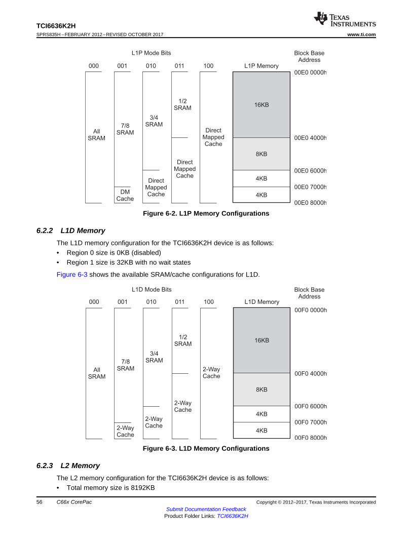
L1D Memory
00F0 0000h
00F0 4000h
00F0 6000h
00F0 7000h
00F0 8000h
1/2SRAM
2-WayCache
3/4SRAM7/8
SRAMAllSRAM
000 001 010 011 100
Block BaseAddress
L1D Mode Bits
4KB
8KB
16KB
4KB
2-WayCache
2-WayCache
2-WayCache
4KB
8KB
16KB
L1P Memory00E0 0000h
00E0 4000h
00E0 6000h
00E0 7000h
00E0 8000h
DirectMappedCache
1/2SRAM
DMCache
3/4SRAM7/8
SRAMAllSRAM
000 001 010 011 100
Block BaseAddress
L1P Mode Bits
4KB
DirectMappedCache
DirectMappedCache
56
TCI6636K2HSPRS835H –FEBRUARY 2012–REVISED OCTOBER 2017 www.ti.com
Submit Documentation FeedbackProduct Folder Links: TCI6636K2H
C66x CorePac Copyright © 2012–2017, Texas Instruments Incorporated
Figure 6-2. L1P Memory Configurations
6.2.2 L1D MemoryThe L1D memory configuration for the TCI6636K2H device is as follows:• Region 0 size is 0KB (disabled)• Region 1 size is 32KB with no wait states
Figure 6-3 shows the available SRAM/cache configurations for L1D.
Figure 6-3. L1D Memory Configurations
6.2.3 L2 MemoryThe L2 memory configuration for the TCI6636K2H device is as follows:• Total memory size is 8192KB

512KB
256KB
128KB
64KB
32KB
32KB
L2 Memory
008C 0000h
008E 0000h
008F 0000h
008F 8000h
008F FFFFh
000 001 010 011 100
Block BaseAddress
L2 Mode Bits
1/2SRAM
4-WayCache
101 110
0088 0000h
0080 0000h
4-WayCache4-Way
Cache4-WayCache
ALLSRAM
4-WayCache
4-WayCache
3/4SRAM
7/8SRAM15/16
SRAM31/32SRAM
57
TCI6636K2Hwww.ti.com SPRS835H –FEBRUARY 2012–REVISED OCTOBER 2017
Submit Documentation FeedbackProduct Folder Links: TCI6636K2H
C66x CorePacCopyright © 2012–2017, Texas Instruments Incorporated
• Each CorePac contains 1024KB of memory• Local starting address for each CorePac is 0080 0000h
L2 memory can be configured as all SRAM, all 4-way set-associative cache, or a mix of the two. Theamount of L2 memory that is configured as cache is controlled through the L2MODE field of the L2Configuration Register (L2CFG) of the C66x CorePac. Figure 6-4 shows the available SRAM/cacheconfigurations for L2. By default, L2 is configured as all SRAM after device reset.
Figure 6-4. L2 Memory Configurations
Global addresses that are accessible to all masters in the system are in all memory local to theprocessors. In addition, local memory can be accessed directly by the associated processor throughaliased addresses, where the eight MSBs are masked to 0. The aliasing is handled within the CorePacand allows for common code to be run unmodified on multiple cores. For example, address location0x10800000 is the global base address for CorePac0's L2 memory. CorePac0 can access this location byeither using 0x10800000 or 0x00800000. Any other master on the device must use 0x10800000 only.Conversely, 0x00800000 can by used by any of the C66x CorePacs as their own L2 base addresses. For

58
TCI6636K2HSPRS835H –FEBRUARY 2012–REVISED OCTOBER 2017 www.ti.com
Submit Documentation FeedbackProduct Folder Links: TCI6636K2H
C66x CorePac Copyright © 2012–2017, Texas Instruments Incorporated
(1) x = 0, 1, 2, 3, 4, 5
CorePac0, as mentioned, this is equivalent to 0x10800000, for CorePac1 this is equivalent to0x11800000, and for CorePac2 this is equivalent to 0x12800000. Local addresses should be used only forshared code or data, allowing a single image to be included in memory. Any code/data targeted to aspecific core, or a memory region allocated during run time by a particular CorePac should always use theglobal address only.
6.2.4 Multicore Shared Memory SRAMThe MSM SRAM configuration for the TCI6636K2H device is as follows:• Memory size of 6144KB• Can be configured as shared L2 or shared L3 memory• Allows extension of external addresses from 2GB up to 8GB• Has built-in memory protection features
The MSM SRAM is always configured as all SRAM. When configured as a shared L2, its contents can becached in L1P and L1D. When configured in shared L3 mode, it’s contents can be cached in L2 also. Formore details on external memory address extension and memory protection features, see the KeyStoneArchitecture Multicore Shared Memory Controller (MSMC) User's Guide.
6.2.5 L3 MemoryThe L3 ROM on the device is 128KB. The ROM contains software used to boot the device. There is norequirement to block accesses from this portion to the ROM.
6.3 Memory ProtectionMemory protection allows an operating system to define who or what is authorized to access L1D, L1P,and L2 memory. To accomplish this, the L1D, L1P, and L2 memories are divided into pages. There are 16pages of L1P (2KB each), 16 pages of L1D (2KB each), and 32 pages of L2 (32KB each). The L1D, L1P,and L2 memory controllers in the C66x CorePac are equipped with a set of registers that specify thepermissions for each memory page.
Each page may be assigned with fully orthogonal user and supervisor read, write, and executepermissions. In addition, a page may be marked as either (or both) locally accessible or globallyaccessible. A local access is a direct DSP access to L1D, L1P, and L2, while a global access is initiatedby a DMA (either IDMA or the EDMA3) or by other system masters. Note that EDMA or IDMA transfersprogrammed by the DSP count as global accesses. On a secure device, pages can be restricted to secureaccess only (default) or opened up for public, nonsecure access.
The DSP and each of the system masters on the device are all assigned a privilege ID. It is possible tospecify only whether memory pages are locally or globally accessible.
The AIDx and LOCAL bits of the memory protection page attribute registers specify the memory pageprotection scheme, see Table 6-1.
Table 6-1. Available Memory Page Protection Schemes
AIDx BIT (1) LOCAL BIT DESCRIPTION0 0 No access to memory page is permitted.0 1 Only direct access by DSP is permitted.1 0 Only accesses by system masters and IDMA are permitted (includes EDMA and IDMA accesses initiated by
the DSP).1 1 All accesses permitted.

59
TCI6636K2Hwww.ti.com SPRS835H –FEBRUARY 2012–REVISED OCTOBER 2017
Submit Documentation FeedbackProduct Folder Links: TCI6636K2H
C66x CorePacCopyright © 2012–2017, Texas Instruments Incorporated
Faults are handled by software in an interrupt (or an exception, programmable within the CorePacinterrupt controller) service routine. A DSP or DMA access to a page without the proper permissions will:• Block the access — reads return 0, writes are ignored• Capture the initiator in a status register — ID, address, and access type are stored• Signal the event to the DSP interrupt controller
The software is responsible for taking corrective action to respond to the event and resetting the errorstatus in the memory controller. For more information on memory protection for L1D, L1P, and L2, see theTMS320C66x DSP CorePac User's Guide.
6.4 Bandwidth ManagementWhen multiple requestors contend for a single C66x CorePac resource, the conflict is resolved by grantingaccess to the highest priority requestor. The following four resources are managed by the bandwidthmanagement control hardware:• Level 1 Program (L1P) SRAM/Cache• Level 1 Data (L1D) SRAM/Cache• Level 2 (L2) SRAM/Cache• Memory-mapped registers configuration bus
The priority level for operations initiated within the C66x CorePac are declared through registers in theCorePac. These operations are:• DSP-initiated transfers• User-programmed cache coherency operations• IDMA-initiated transfers
The priority level for operations initiated outside the CorePac by system peripherals is declared throughthe Priority Allocation Register (PRI_ALLOC). System peripherals with no fields in PRI_ALLOC have theirown registers to program their priorities.
More information on the bandwidth management features of the CorePac can be found in theTMS320C66x DSP CorePac User's Guide.
6.5 Power-Down ControlThe C66x CorePac supports the ability to power-down various parts of the CorePac. The power-downcontroller (PDC) of the CorePac can be used to power down L1P, the cache control hardware, the DSP,and the entire CorePac. These power-down features can be used to design systems for lower overallsystem power requirements.
NOTEThe TCI6636K2H does not support power-down modes for the L2 memory at this time.
More information on the power-down features of the C66x CorePac can be found in the TMS320C66xDSP CorePac User's Guide.

60
TCI6636K2HSPRS835H –FEBRUARY 2012–REVISED OCTOBER 2017 www.ti.com
Submit Documentation FeedbackProduct Folder Links: TCI6636K2H
C66x CorePac Copyright © 2012–2017, Texas Instruments Incorporated
6.6 C66x CorePac RevisionThe version and revision of the C66x CorePac can be read from the CorePac Revision ID Register(MM_REVID) at address 0181 2000h. The MM_REVID register is shown in Figure 6-5 and described inTable 6-2. The C66x CorePac revision is dependent on the silicon revision being used.
Figure 6-5. CorePac Revision ID Register (MM_REVID)31 30 29 28 27 26 25 24 23 22 21 20 19 18 17 16 15 14 13 12 11 10 9 8 7 6 5 4 3 2 1 0
VERSION REVISIONR-n R-n
Legend: R = Read only; R/W = Read/Write; -n = value after reset
Table 6-2. CorePac Revision ID Register (MM_REVID) Field DescriptionsBit Name Value Description31-16 VERSION 0009h Version of the C66x CorePac implemented on the device.15-0 REVISION xxxxh Revision of the C66x CorePac version implemented on this device.
0000h = silicon revision 1.00002h = silicon revision 1.10003h = silicon revisions 2.0, 3.0, and 3.1
6.7 C66x CorePac Register DescriptionsSee the TMS320C66x DSP CorePac User's Guide for register offsets and definitions.

32KB L1P-Cache
32KB L1D-Cache
ARMA15
32KB L1P-Cache
32KB L1D-Cache
ARMA15
32KB L1P-Cache
32KB L1D-Cache
ARMA15
32KB L1P-Cache
32KB L1D-Cache
ARMA15
L2
Ca
ch
e C
on
tro
l a
nd
Sn
oo
p C
on
tro
l U
nit
4 M
B L
2 C
ac
he
Tim
er
0 -
3
GenericInterruptController
400
GlobalTime Base
Counter
VBUSP2AXIBridge
ARM INTC
KeyStone II ARM CorePac (Quad Core)
TeraNet(CFG)
480 SPIInterrupts
IRQ,FIQ,
VIRQ,VFIQ
16PPI
64Bits
Debug
CTM
CTI (´4)AXI-VBUS
Master
ARMTrace
ATB
PTM (´4)
APB MUX
DebugSubSystem
APB APB
ATB
OCP
VBUSP TeraNet(DMA)
256bVBUSM MSMC
DDR3
ARMVBUSP
Registers
VBUSP TeraNet(CFG)
Boot Config Main PLL ARM PLL PSC
EndianCFG
ARMCorePac
Clock
ARMA15 Core
Clock
ARM
ATB
CTI/CTM
STM
APB
ARM Cluster
Copyright © 2016, Texas Instruments Incorporated
61
TCI6636K2Hwww.ti.com SPRS835H –FEBRUARY 2012–REVISED OCTOBER 2017
Submit Documentation FeedbackProduct Folder Links: TCI6636K2H
ARM CorePacCopyright © 2012–2017, Texas Instruments Incorporated
7 ARM CorePac
The ARM CorePac is added in the TCI6636K2H to enable the ability for layer 2 and layer 3 processing on-chip. Operations such as traffic control, local O&M, NBAP/FP termination, and SCTP processing can allbe performed with the Cortex-A15 processor core.
The ARM CorePac of the TCI6636K2H integrates one or more Cortex-A15 processor clusters withadditional logic for bus protocol conversion, emulation, interrupt handling, and debug relatedenhancements. The Cortex-A15 processor is an ARMv7A-compatible, multi-issue out-of-order superscalarexecution engine with integrated L1 caches. The implementation also supports advanced SIMDv2 (NEONtechnology) and VFPv4 (vector floating point) architecture extensions, security, virtualization, LPAE (largephysical address extension), and multiprocessing extensions. The ARM CorePac includes a 4MB L2cache and support for AMBA4 AXI and AXI coherence extension (ACE) protocols. An interrupt controller isincluded in the ARM CorePac to handle host interrupt requests in the system. For more information, seethe KeyStone II Architecture ARM CorePac User's Guide.
The ARM CorePac has three functional clock domains, including a high-frequency clock domain used bythe Cortex-A15. The high-frequency domain is isolated from the rest of the device by asynchronousbridges.
Figure 7-1 shows an overall view of the Quad ARM CorePac.
Figure 7-1. KeyStone™ II SoCARM CorePac Block Diagram
62
TCI6636K2HSPRS835H –FEBRUARY 2012–REVISED OCTOBER 2017 www.ti.com
Submit Documentation FeedbackProduct Folder Links: TCI6636K2H
ARM CorePac Copyright © 2012–2017, Texas Instruments Incorporated
7.1 FeaturesThe key features of the Quad Core ARM CorePac are as follows:• One or more Cortex-A15 processors, each containing:
– Cortex-A15 processor revision R2P4.– ARM architecture version 7 ISA.– Multi-issue, out-of-order, superscalar pipeline.– L1 and L2 instruction and data cache of 32KB, 2-way, 16 word line with 128-bit interface.– Integrated L2 cache of 4MB, 16-way, 16-word line, 128-bit interface to L1 along with ECC/parity.– Includes the NEON™ media coprocessor (NEON), which implements the advanced SIMDv2 media
processing architecture and the VFPv4 Vector Floating Point architecture.– The external interface uses the AXI protocol configured to 128-bit data width.– Includes the System Trace Macrocell (STM) support for noninvasive debugging.– Implements the ARMv7 debug with watchpoint and breakpoint registers and 32-bit advanced
peripheral bus (APB) slave interface to CoreSight™ debug systems.• Interrupt controller
– Supports up to 480 interrupt requests• Emulation/debug
– Compatible with CoreSight architecture• Clock generation
– Through the dedicated ARM PLL
7.2 System IntegrationThe ARM CorePac integrates the following group of submodules.• Cortex-A15 Processors: Provides a high processing capability, including the NEON technology for
mobile multimedia acceleration. The Cortex-A15 communicates with the rest of the ARM CorePacthrough an AXI bus with an AXI2VBUSM bridge and receives interrupts from the ARM CorePacinterrupt controller (ARM INTC).
• Interrupt Controller: Handles interrupts from modules outside of the ARM CorePac (for details, seeSection 7.3.3).
• Clock Divider: Provides the required divided clocks to the internal modules of the ARM CorePac andhas a clock input from the ARM PLL and the Main PLL
• In-Circuit Emulator: Fully compatible with CoreSight architecture and enables debugging capabilities.
7.3 ARM Cortex-A15 Processor
7.3.1 OverviewThe ARM Cortex-A15 processor incorporates the technologies available in the ARM7™ architecture.These technologies include NEON for media and signal processing and Jazelle® RCT for acceleration ofreal-time compilers, Thumb®-2 technology for code density, and the VFPv4 floating point architecture. Fordetails, see the ARM Cortex-A15 Processor Technical Reference Manual.
7.3.2 FeaturesTable 7-1 shows the features supported by the Cortex-A15 processor core.
Table 7-1. Cortex-A15 Processor Core Supported Features
FEATURES DESCRIPTIONARM version 7-A ISA Standard Cortex-A15 processor instruction set + Thumb2, ThumbEE, JazelleX Java accelerator, and
media extensionsBackward compatible with previous ARM ISA versions

63
TCI6636K2Hwww.ti.com SPRS835H –FEBRUARY 2012–REVISED OCTOBER 2017
Submit Documentation FeedbackProduct Folder Links: TCI6636K2H
ARM CorePacCopyright © 2012–2017, Texas Instruments Incorporated
Table 7-1. Cortex-A15 Processor Core Supported Features (continued)FEATURES DESCRIPTIONCortex-A15 processor version R2P4Integer core Main core for processing integer instructionsNEON core Gives greatly enhanced throughput for media workloads and VFP-Lite supportArchitecture Extensions Security, virtualization and LPAE (40-bit physical address) extensionsL1 Lcache and Dcache 32KB, 2-way, 16 word line, 128 bit interfaceL2 cache 4096KB, 16-way, 16 word line, 128 bit interface to L1, ECC/Parity is supported shared between cores
L2 valid bits cleared by software loop or by hardwareCache Coherency Support for coherent memory accesses between A15 cores and other noncore master peripherals
(Ex: EDMA) in the DDR3A and MSMC SRAM space.Branch target address cache Dynamic branch prediction with Branch Target Buffer (BTB) and Global History Buffer (GHB), a return
stack, and an indirect predictorEnhanced memory managementunit
Mapping sizes are 4KB, 64KB, 1MB, and 16MB
Buses 128b AXI4 internal bus from Cortex-A15 converted to a 256b VBUSM to interface (through theMSMC) with MSMC SRAM, DDR EMIF, ROM, Interrupt controller and other system peripherals
Noninvasive Debug Support Processor instruction trace using 4x Program Trace Macrocell (CoreSight PTM), Data trace (print-fstyle debug) using System Trace Macrocell (CoreSight STM) and Performance Monitoring Units(PMU)
Misc Debug Support JTAG based debug and Cross triggeringClocking Dedicated ARM PLL for flexible clocking scenariosVoltage SmartReflex voltage domain for automatic voltage scalingPower Support for standby modes and separate core power domains for additional leakage power reduction
7.3.3 ARM Interrupt ControllerThe ARM CorePac interrupt controller (AINTC) is responsible for prioritizing all service requests from thesystem peripherals and the secondary interrupt controller CIC2 and then generating either nIRQ or nFIQto the Cortex-A15 processor. The type of the interrupt (nIRQ or nFIQ) and the priority of the interruptinputs are programmable. The AINTC interfaces to the Cortex-A15 processor via the AXI port through anVBUS2AXI bridge and runs at half the processor speed. It has the capability to handle up to 480 requests,which can be steered/prioritized as A15 nFIQ or nIRQ interrupt requests.
The general features of the AINTC are:• Up to 480 level sensitive shared peripheral interrupts (SPI) inputs• Individual priority for each interrupt input• Each interrupt can be steered to nFIQ or nIRQ• Independent priority sorting for nFIQ and nIRQ• Secure mask flag
On the chip level, there is a dedicated chip level interrupt controller to serve the ARM interrupt controller.See Section 8.3 for more details.
Figure 7-2 shows an overall view of the ARM CorePac Interrupt Controller.
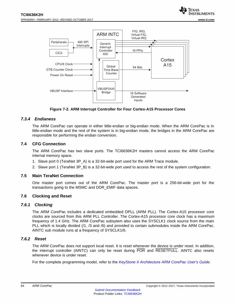
CortexA15
FIQ, IRQ,Virtual FIQ,Virtual IRQ
16 PPIs
GenericInterruptController
400
GlobalTime Base
Counter
64 Bits
Peripherals
CIC2
480 SPIInterrupts
VBUSP2AXIBridge
ARM INTC
16 SoftwareGenerated
Inputs
VBUSP Interface
CPU/6 Clock
GTB Counter Clock
Power On Reset
64
TCI6636K2HSPRS835H –FEBRUARY 2012–REVISED OCTOBER 2017 www.ti.com
Submit Documentation FeedbackProduct Folder Links: TCI6636K2H
ARM CorePac Copyright © 2012–2017, Texas Instruments Incorporated
Figure 7-2. ARM Interrupt Controller for Four Cortex-A15 Processor Cores
7.3.4 EndianessThe ARM CorePac can operate in either little-endian or big-endian mode. When the ARM CorePac is inlittle-endian mode and the rest of the system is in big-endian mode, the bridges in the ARM CorePac areresponsible for performing the endian conversion.
7.4 CFG ConnectionThe ARM CorePac has two slave ports. The TCI6636K2H masters cannot access the ARM CorePacinternal memory space.1. Slave port 0 (TeraNet 3P_A) is a 32-bit-wide port used for the ARM Trace module.2. Slave port 1 (TeraNet 3P_B) is a 32-bit-wide port used to access the rest of the system configuration.
7.5 Main TeraNet ConnectionOne master port comes out of the ARM CorePac. The master port is a 256-bit-wide port for thetransactions going to the MSMC and DDR_EMIF data spaces.
7.6 Clocking and Reset
7.6.1 ClockingThe ARM CorePac includes a dedicated embedded DPLL (ARM PLL). The Cortex-A15 processor coreclocks are sourced from this ARM PLL Controller. The Cortex-A15 processor core clock has a maximumfrequency of 1.4 GHz. The ARM CorePac subsytem also uses the SYSCLK1 clock source from the mainPLL which is locally divided (/1, /3 and /6) and provided to certain submodules inside the ARM CorePac.AINTC sub module runs at a frequency of SYSCLK1/6.
7.6.2 ResetThe ARM CorePac does not support local reset. It is reset whenever the device is under reset. In addition,the interrupt controller (AINTC) can only be reset during POR and RESETFULL. AINTC also resetswhenever device is under reset.
For the complete programming model, refer to the KeyStone II Architecture ARM CorePac User's Guide.

65
TCI6636K2Hwww.ti.com SPRS835H –FEBRUARY 2012–REVISED OCTOBER 2017
Submit Documentation FeedbackProduct Folder Links: TCI6636K2H
Memory, Interrupts, and EDMA for TCI6636K2HCopyright © 2012–2017, Texas Instruments Incorporated
8 Memory, Interrupts, and EDMA for TCI6636K2H
8.1 Memory Map Summary for TCI6636K2HTable 8-1 shows the memory map address ranges of the device.
Table 8-1. Device Memory Map Summary for TCI6636K2HPHYSICAL 40-BIT ADDRESS
BYTES ARM VIEW DSP VIEW SOC VIEWSTART END
00 0000 0000 00 0003 FFFF 256K ARM ROM Reserved ARM ROM
00 0004 0000 00 007F FFFF 8M-256K Reserved Reserved Reserved
00 0080 0000 00 008F FFFF 1M Reserved L2 SRAM L2 SRAM
00 0090 0000 00 00DF FFFF 5M Reserved Reserved Reserved
00 00E0 0000 00 00E0 7FFF 32K Reserved L1P SRAM L1P SRAM
00 00E0 8000 00 00EF FFFF 1M-32K Reserved Reserved Reserved
00 00F0 0000 00 00F0 7FFF 32K Reserved L1D SRAM L1D SRAM
00 00F0 8000 00 00FF FFFF 1M-32K Reserved Reserved Reserved
00 0100 0000 00 0100 FFFF 64K ARM AXI2VBUSM Master Registers C66x CorePac registers C66x CorePac registers
00 0101 0000 00 010F FFFF 1M-64K Reserved C66x CorePac registers C66x CorePac registers
00 0110 0000 00 0110 FFFF 64K ARM STM Stimulus Ports C66x CorePac registers C66x CorePac registers
00 0111 0000 00 01BF FFFF 11M-64K Reserved C66x CorePac registers C66x CorePac registers
00 01C0 0000 00 01CF FFFF 1M Reserved Reserved Reserved
00 01D0 0000 00 01D0 007F 128 Tracer_M SMC0_CFG Tracer_MSMC0_CFG Tracer_MSMC0_CFG
00 01D0 0080 00 01D0 7FFF 32K-128 Reserved Reserved Reserved
00 01D0 8000 00 01D0 807F 128 Tracer_MSMC1_CFG Tracer_MSMC1_CFG Tracer_MSMC1_CFG
00 01D0 8080 00 01D0 FFFF 32K-128 Reserved Reserved Reserved
00 01D1 0000 00 01D1 007F 128 Tracer_MSMC2_CFG Tracer_MSMC2_CFG Tracer_MSMC2_CFG
00 01D1 0080 00 01D1 7FFF 32K-128 Reserved Reserved Reserved
00 01D1 8000 00 01D1 807F 128 Tracer_MSMC3_CFG Tracer_MSMC3_CFG Tracer_MSMC3_CFG
00 01D1 8080 00 01D1 FFFF 32K-128 Reserved Reserved Reserved
00 01D2 0000 00 01D2 007F 128 Tracer_QM_M_CFG Tracer_QM_M_CFG Tracer_QM_M_CFG
00 01D2 0080 00 01D2 7FFF 32K-128 Reserved Reserved Reserved
00 01D2 8000 00 01D2 807F 128 Tracer_DDR3A_CFG Tracer_DDR3A_CFG Tracer_DDR3A_CFG
00 01D2 8080 00 01D2 FFFF 32K-128 Reserved Reserved Reserved
00 01D3 0000 00 01D3 007F 128 Tracer_SM_CFG Tracer_SM_CFG Tracer_SM_CFG
00 01D3 0080 00 01D3 7FFF 32K-128 Reserved Reserved Reserved
00 01D3 8000 00 01D3 807F 128 Tracer_QM_CFG1_CFG Tracer_QM_CFG1_CFG Tracer_QM_CFG1_CFG
00 01D3 8080 00 01D3 FFFF 32K-128 Reserved Reserved Reserved
00 01D4 0000 00 01D4 007F 128 Tracer_CFG_CFG Tracer_CFG_CFG Tracer_CFG_CFG
00 01D4 0080 00 01D4 7FFF 32K-128 Reserved Reserved Reserved
00 01D4 8000 00 01D4 807F 128 Tracer_L2_0_CFG Tracer_L2_0_CFG Tracer_L2_0_CFG
00 01D4 8080 00 01D4 FFFF 32K-128 Reserved Reserved Reserved
00 01D5 0000 00 01D5 007F 128 Tracer_L2_1_CFG Tracer_L2_1_CFG Tracer_L2_1_CFG
00 01D5 0080 00 01D5 7FFF 32K-128 Reserved Reserved Reserved
00 01D5 8000 00 01D5 807F 128 Tracer_L2_2_CFG Tracer_L2_2_CFG Tracer_L2_2_CFG
00 01D5 8080 00 01D5 FFFF 32K-128 Reserved Reserved Reserved
00 01D6 0000 00 01D6 007F 128 Tracer_L2_3_CFG Tracer_L2_3_CFG Tracer_L2_3_CFG
00 01D6 0080 00 01D6 7FFF 32K-128 Reserved Reserved Reserved
00 01D6 8000 00 01D6 807F 128 Tracer_L2_4_CFG Tracer_L2_4_CFG Tracer_L2_4_CFG
00 01D6 8080 00 01D6 FFFF 32K-128 Reserved Reserved Reserved
00 01D7 0000 00 01D7 007F 128 Tracer_L2_5_CFG Tracer_L2_5_CFG Tracer_L2_5_CFG
00 01D7 0080 00 01D7 7FFF 32K-128 Reserved Reserved Reserved
00 01D7 8000 00 01D7 807F 128 Tracer_L2_6_CFG Tracer_L2_6_CFG Tracer_L2_6_CFG
00 01D7 8080 00 01D7 FFFF 32K-128 Reserved Reserved Reserved

66
TCI6636K2HSPRS835H –FEBRUARY 2012–REVISED OCTOBER 2017 www.ti.com
Submit Documentation FeedbackProduct Folder Links: TCI6636K2H
Memory, Interrupts, and EDMA for TCI6636K2H Copyright © 2012–2017, Texas Instruments Incorporated
Table 8-1. Device Memory Map Summary for TCI6636K2H (continued)PHYSICAL 40-BIT ADDRESS
BYTES ARM VIEW DSP VIEW SOC VIEWSTART END
00 01D8 0000 00 01D8 007F 128 Tracer_L2_7_CFG Tracer_L2_7_CFG Tracer_L2_7_CFG
00 01D8 0080 00 01D8 7FFF 32K-128 Reserved Reserved Reserved
00 01D8 8000 00 01D8 807F 128 Tracer_RAC_FEI_CFG Tracer_RAC_FEI_CFG Tracer_RAC_FEI_CFG
00 01D8 8080 00 01D8 8FFF 32K-128 Reserved Reserved Reserved
00 01D9 0000 00 01D9 007F 128 Tracer_RAC_CFG1_CFG Tracer_RAC_CFG1_CFG Tracer_RAC_CFG1_CFG
00 01D9 0080 00 01D9 7FFF 32K-128 Reserved Reserved Reserved
00 01D9 8000 00 01D9 807F 128 Tracer_TAC_BE_CFG Tracer_TAC_BE_CFG Tracer_TAC_BE_CFG
00 01D9 8080 00 01D9 FFFF 32K-128 Reserved Reserved Reserved
00 01DA 0000 00 01DA 007F 128 Tracer_QM_CFG2_CFG Tracer_QM_CFG2_CFG Tracer_QM_CFG2_CFG
00 01DA 0080 00 01DA 7FFF 32K-128 Reserved Reserved Reserved
00 01DA 8000 00 01DA 807F 128 Tracer_RAC_CFG2_CFG Tracer_RAC_CFG2_CFG Tracer_RAC_CFG2_CFG
00 01DA 8080 00 01DA FFFF 32K-128 Reserved Reserved Reserved
00 01DB 0000 00 01DB 007F 128 Tracer_DDR3B_CFG Tracer_DDR3B_CFG Tracer_DDR3B_CFG
00 01DB 0080 00 01DB 7FFF 32K-128 Reserved Reserved Reserved
00 01DB 8000 00 01DB 807F 128 Tracer_BCR_CFG_CFG Tracer_BCR_CFG_CFG Tracer_BCR_CFG_CFG
00 01DB 8080 00 01DB 8FFF 32K-128 Reserved Reserved Reserved
00 01DC 0000 00 01DC 007F 128 Tracer_TPCC0_4_CFG Tracer_TPCC0_4_CFG Tracer_TPCC0_4_CFG
00 01DC 0080 00 01DC 7FFF 32K-128 Reserved Reserved Reserved
00 01DC 8000 00 01DC 807F 128 Tracer_TPCC1_2_3_CFG Tracer_TPCC1_2_3_CFG Tracer_TPCC1_2_3_CFG
00 01DC 8080 00 01DC FFFF 32K-128 Reserved Reserved Reserved
00 01DD 0000 00 01DD 007F 128 Tracer_INTC_CFG Tracer_INTC_CFG Tracer_INTC_CFG
00 01DD 0080 00 01DD 7FFF 32K-128 Reserved Reserved Reserved
00 01DD 8000 00 01DD 807F 128 Tracer_MSMC4_CFG Tracer_MSMC4_CFG Tracer_MSMC4_CFG
00 01DD 8080 00 01DD FFFF 32K-128 Reserved Reserved Reserved
00 01DE 0000 00 01DE 007F 128 Tracer_MSMC5_CFG Tracer_MSMC5_CFG Tracer_MSMC5_CFG
00 01DE 0080 00 01DE 03FF 1K-128 Reserved Reserved Reserved
00 01DE 0400 00 01DE 047F 128 Tracer_MSMC6_CFG Tracer_MSMC6_CFG Tracer_MSMC6_CFG
00 01DD 0480 00 01DD 07FF 1K-128 Reserved Reserved Reserved
00 01DE 0800 00 01DE 087F 128 Tracer_MSMC7_CFG Tracer_MSMC7_CFG Tracer_MSMC7_CFG
00 01DE 0880 00 01DE 7FFF 30K-128 Reserved Reserved Reserved
00 01DE 8000 00 01DE 807F 128 Tracer_SPI_ROM_EMIF16_CFG Tracer_SPI_ROM_EMIF16_CFG Tracer_SPI_ROM_EMIF16_CFG
00 01DE 8080 00 01DF FFFF 64K-128 Reserved Reserved Reserved
00 01E0 0000 00 01E3 FFFF 256K Reserved Reserved Reserved
00 01E4 0000 00 01E4 3FFF 16K Reserved Reserved Reserved
00 01E4 4000 00 01E7 FFFF 240k Reserved Reserved Reserved
00 01E8 0000 00 01E8 3FFF 16K ARM CorePac VBUSP MemoryMapped Registers
ARM CorePac VBUSP MemoryMapped Registers
ARM CorePac VBUSP MemoryMapped Registers
00 01E8 4000 00 01EB FFFF 240k Reserved Reserved Reserved
00 01EC 0000 00 01EF FFFF 256K Reserved Reserved Reserved
00 01F0 0000 00 01F7 FFFF 512K AIF2 control AIF2 control AIF2 control
00 01F8 0000 00 01F8 FFFF 64K RAC_1 - FEI control RAC_1 - FEI control RAC_1 - FEI control
00 01F9 0000 00 01F9 FFFF 64K RAC_1 - BEI control RAC_1 - BEI control RAC_1 - BEI control
00 01FA 0000 00 01FB FFFF 128K RAC_1 - GCCP 0 control RAC_1 - GCCP 0 control RAC_1 - GCCP 0 control
00 01FC 0000 00 01FD FFFF 128K RAC_1 - GCCP 1 control RAC_1 - GCCP 1 control RAC_1 - GCCP 1 control
00 01FE 0000 00 01FF FFFF 128K Reserved Reserved Reserved
00 0200 0000 00 020F FFFF 1M Network Coprocessor (PacketAccelerator, 1-gigabit Ethernetswitch subsystem and SecurityAccelerator)
Network Coprocessor (PacketAccelerator, 1-gigabit Ethernetswitch subsystem and SecurityAccelerator)
Network Coprocessor (PacketAccelerator, 1-gigabit Ethernetswitch subsystem and SecurityAccelerator)
00 0210 0000 00 0210 FFFF 64K RAC_0 - FEI control RAC_0 - FEI control RAC_0 - FEI control
00 0211 0000 00 0211 FFFF 64K RAC_0 - BEI control RAC_0 - BEI control RAC_0 - BEI control
00 0212 0000 00 0213 FFFF 128K RAC_0 - GCCP 0 control RAC_0 - GCCP 0 control RAC_0 - GCCP 0 control

67
TCI6636K2Hwww.ti.com SPRS835H –FEBRUARY 2012–REVISED OCTOBER 2017
Submit Documentation FeedbackProduct Folder Links: TCI6636K2H
Memory, Interrupts, and EDMA for TCI6636K2HCopyright © 2012–2017, Texas Instruments Incorporated
Table 8-1. Device Memory Map Summary for TCI6636K2H (continued)PHYSICAL 40-BIT ADDRESS
BYTES ARM VIEW DSP VIEW SOC VIEWSTART END
00 0214 0000 00 0215 FFFF 128K RAC_0 - GCCP 1 control RAC_0 - GCCP 1 control RAC_0 - GCCP 1 control
00 0216 0000 00 0217 FFFF 128K Reserved Reserved Reserved
00 0218 0000 00 0218 7FFF 32k Reserved Reserved Reserved
00 0218 8000 00 0218 FFFF 32k Reserved Reserved Reserved
00 0219 0000 00 0219 FFFF 64k Reserved Reserved Reserved
00 021A 0000 00 021A FFFF 64K Reserved Reserved Reserved
00 021B 0000 00 021B FFFF 64K Reserved Reserved Reserved
00 021C 0000 00 021C 03FF 1K TCP3d_0 TCP3d_0 TCP3d_0
00 021C 0400 00 021C 3FFF 15K Reserved Reserved Reserved
00 021C 4000 00 021C 43FF 1K Reserved Reserved Reserved
00 021C 4400 00 021C 5FFF 7K Reserved Reserved Reserved
00 021C 6000 00 021C 63FF 1K Reserved Reserved Reserved
00 021C 6400 00 021C 7FFF 7K Reserved Reserved Reserved
00 021C 8000 00 021C 83FF 1K TCP3d_1 TCP3d_1 TCP3d_1
00 021C 8400 00 021C FFFF 31K Reserved Reserved Reserved
00 021D 0000 00 021D 00FF 256 VCP2_0 configuration VCP2_0 configuration VCP2_0 configuration
00 021D 0100 00 021D 3FFF 16K Reserved Reserved Reserved
00 021D 4000 00 021D 40FF 256 VCP2_1 configuration VCP2_1 configuration VCP2_1 configuration
00 021D 4100 00 021D 7FFF 16K Reserved Reserved Reserved
00 021D 8000 00 021D 80FF 256 VCP2_2 configuration VCP2_2 configuration VCP2_2 configuration
00 021D 8100 00 021D BFFF 16K Reserved Reserved Reserved
00 021D C000 00 021D C0FF 256 VCP2_3 configuration VCP2_3 configuration VCP2_3 configuration
00 021D C100 00 021D EFFF 12K-256 Reserved Reserved Reserved
00 021D F000 00 021D F07F 128 USIM configuration USIM configuration USIM configuration
00 021D F080 00 021D FFFF 4K-128 Reserved Reserved Reserved
00 021E 0000 00 021E FFFF 64K Reserved Reserved Reserved
00 021F 0000 00 021F 07FF 2K FFTC_0 configuration FFTC_0 configuration FFTC_0 configuration
00 021F 0800 00 021F 0FFF 2K Reserved Reserved Reserved
00 021F 1000 00 021F 17FF 2K Reserved Reserved Reserved
00 021F 1800 00 021F 3FFF 10K Reserved Reserved Reserved
00 021F 4000 00 021F 47FF 2K FFTC_1 configuration FFTC_1 configuration FFTC_1 configuration
00 021F 4800 00 021F 7FFF 14K Reserved Reserved Reserved
00 021F 8000 00 021F 87FF 2K FFTC_2 configuration FFTC_2 configuration FFTC_2 configuration
00 021F 8800 00 021F BFFF 14K Reserved Reserved Reserved
00 021F C000 00 021F C7FF 2K FFTC_3 configuration FFTC_3 configuration FFTC_3 configuration
00 021F C800 00 021F FFFF 14K Reserved Reserved Reserved
00 0220 0000 00 0220 007F 128 Timer0 Timer0 Timer0
00 0220 0080 00 0220 FFFF 64K-128 Reserved Reserved Reserved
00 0221 0000 00 0221 007F 128 Timer1 Timer1 Timer1
00 0221 0080 00 0221 FFFF 64K-128 Reserved Reserved Reserved
00 0222 0000 00 0222 007F 128 Timer2 Timer2 Timer2
00 0222 0080 00 0222 FFFF 64K-128 Reserved Reserved Reserved
00 0223 0000 00 0223 007F 128 Timer3 Timer3 Timer3
00 0223 0080 00 0223 FFFF 64K-128 Reserved Reserved Reserved
00 0224 0000 00 0224 007F 128 Timer4 Timer4 Timer4
00 0224 0080 00 0224 FFFF 64K-128 Reserved Reserved Reserved
00 0225 0000 00 0225 007F 128 Timer5 Timer5 Timer5
00 0225 0080 00 0225 FFFF 64K-128 Reserved Reserved Reserved
00 0226 0000 00 0226 007F 128 Timer6 Timer6 Timer6
00 0226 0080 00 0226 FFFF 64K-128 Reserved Reserved Reserved

68
TCI6636K2HSPRS835H –FEBRUARY 2012–REVISED OCTOBER 2017 www.ti.com
Submit Documentation FeedbackProduct Folder Links: TCI6636K2H
Memory, Interrupts, and EDMA for TCI6636K2H Copyright © 2012–2017, Texas Instruments Incorporated
Table 8-1. Device Memory Map Summary for TCI6636K2H (continued)PHYSICAL 40-BIT ADDRESS
BYTES ARM VIEW DSP VIEW SOC VIEWSTART END
00 0227 0000 00 0227 007F 128 Timer7 Timer7 Timer7
00 0227 0080 00 0227 FFFF 64K-128 Reserved Reserved Reserved
00 0228 0000 00 0228 007F 128 Timer 8 Timer 8 Timer 8
00 0228 0080 00 0228 FFFF 64K-128 Reserved Reserved Reserved
00 0229 0000 00 0229 007F 128 Timer 9 Timer 9 Timer 9
00 0229 0080 00 0229 FFFF 64K-128 Reserved Reserved Reserved
00 022A 0000 00 022A 007F 128 Timer 10 Timer 10 Timer 10
00 022A 0080 00 022A FFFF 64K-128 Reserved Reserved Reserved
00 022B 0000 00 022B 007F 128 Timer 11 Timer 11 Timer 11
00 022B 0080 00 022B FFFF 64K-128 Reserved Reserved Reserved
00 022C 0000 00 022C 007F 128 Timer 12 Timer 12 Timer 12
00 022C 0080 00 022C FFFF 64K-128 Reserved Reserved Reserved
00 022D 0000 00 022D 007F 128 Timer 13 Timer 13 Timer 13
00 022D 0080 00 022D FFFF 64K-128 Reserved Reserved Reserved
00 022E 0000 00 022E 007F 128 Timer 14 Timer 14 Timer 14
00 022E 0080 00 022E FFFF 64K-128 Reserved Reserved Reserved
00 022F 0000 00 022F 007F 128 Timer 15 Timer 15 Timer 15
00 022F 0080 00 022F 00FF 128 Timer 16 Timer 16 Timer 16
00 022F 0100 00 022F 017F 128 Timer 17 Timer 17 Timer 17
00 022F 0180 00 022F 01FF 128 Timer 18 Timer 18 Timer 18
00 022F 0200 00 022F 027F 128 Timer 19 Timer 19 Timer 19
00 0230 0000 00 0230 FFFF 64K Reserved Reserved Reserved
00 0231 0000 00 0231 01FF 512 PLL Controller PLL Controller PLL Controller
00 0231 0200 00 0231 9FFF 40K-512 Reserved Reserved Reserved
00 0231 A000 00 0231 BFFF 8K HyperLink0 SerDes Config HyperLink0 SerDes Config HyperLink0 SerDes Config
00 0231 C000 00 0231 DFFF 8K HyperLink1 SerDes Config HyperLink1 SerDes Config HyperLink1 SerDes Config
00 0231 E000 00 0231 FFFF 8K Reserved Reserved Reserved
00 0232 0000 00 0232 3FFF 16K PCIE SerDes Config PCIE SerDes Config PCIE SerDes Config
00 0232 4000 00 0232 5FFF 8K AIF2 SerDes B4 Config AIF2 SerDes B4 Config AIF2 SerDes B4 Config
00 0232 6000 00 0232 7FFF 8K AIF2 SerDes B8 Config AIF2 SerDes B8 Config AIF2 SerDes B8 Config
00 0232 8000 00 0232 8FFF 4K DDRB PHY Config DDRB PHY Config DDRB PHY Config
00 0232 9000 00 0232 9FFF 4K DDRA PHY Config DDRA PHY Config DDRA PHY Config
00 0232 A000 00 0232 BFFF 8K SGMII SerDes Config SGMII SerDes Config SGMII SerDes Config
00 0232 C000 00 0232 DFFF 8K SRIO SerDes Config SRIO SerDes Config SRIO SerDes Config
00 0232 E000 00 0232 EFFF 4K Reserved Reserved Reserved
00 0232 F000 00 0232 FFFF 4K Reserved Reserved Reserved
00 0233 0000 00 0233 03FF 1K SmartReflex0 SmartReflex0 SmartReflex0
00 0233 0400 00 0233 07FF 1K SmartReflex1 SmartReflex1 SmartReflex1
00 0233 0400 00 0233 FFFF 62K Reserved Reserved Reserved
00 0234 0000 00 0234 00FF 256 Reserved Reserved Reserved
00 0234 0100 00 0234 3FFF 16K Reserved Reserved Reserved
00 0234 4000 00 0234 40FF 256 Reserved Reserved Reserved
00 0234 4100 00 0234 7FFF 16K Reserved Reserved Reserved
00 0234 8000 00 0234 80FF 256 Reserved Reserved Reserved
00 0234 8100 00 0234 BFFF 16K Reserved Reserved Reserved
00 0234 C000 00 0234 C0FF 256 Reserved Reserved Reserved
00 0234 C100 00 0234 FFFF 16K Reserved Reserved Reserved
00 0235 0000 00 0235 0FFF 4K Power sleep controller (PSC) Power sleep controller (PSC) Power sleep controller (PSC)
00 0235 1000 00 0235 FFFF 64K-4K Reserved Reserved Reserved
00 0236 0000 00 0236 03FF 1K Memory protection unit (MPU) 0 Memory protection unit (MPU) 0 Memory protection unit (MPU) 0

69
TCI6636K2Hwww.ti.com SPRS835H –FEBRUARY 2012–REVISED OCTOBER 2017
Submit Documentation FeedbackProduct Folder Links: TCI6636K2H
Memory, Interrupts, and EDMA for TCI6636K2HCopyright © 2012–2017, Texas Instruments Incorporated
Table 8-1. Device Memory Map Summary for TCI6636K2H (continued)PHYSICAL 40-BIT ADDRESS
BYTES ARM VIEW DSP VIEW SOC VIEWSTART END
00 0236 0400 00 0236 7FFF 31K Reserved Reserved Reserved
00 0236 8000 00 0236 83FF 1K Memory protection unit (MPU) 1 Memory protection unit (MPU) 1 Memory protection unit (MPU) 1
00 0236 8400 00 0236 FFFF 31K Reserved Reserved Reserved
00 0237 0000 00 0237 03FF 1K Memory protection unit (MPU) 2 Memory protection unit (MPU) 2 Memory protection unit (MPU) 2
00 0237 0400 00 0237 7FFF 31K Reserved Reserved Reserved
00 0237 8000 00 0237 83FF 1K Memory protection unit (MPU) 3 Memory protection unit (MPU) 3 Memory protection unit (MPU) 3
00 0237 8400 00 0237 FFFF 31K Reserved Reserved Reserved
00 0238 0000 00 0238 03FF 1K Memory protection unit (MPU) 4 Memory protection unit (MPU) 4 Memory protection unit (MPU) 4
00 0238 8000 00 0238 83FF 1K Memory protection unit (MPU) 5 Memory protection unit (MPU) 5 Memory protection unit (MPU) 5
00 0238 8400 00 0238 87FF 1K Memory protection unit (MPU) 6 Memory protection unit (MPU) 6 Memory protection unit (MPU) 6
00 0238 8800 00 0238 8BFF 1K Memory protection unit (MPU) 7 Memory protection unit (MPU) 7 Memory protection unit (MPU) 7
00 0238 8C00 00 0238 8FFF 1K Memory protection unit (MPU) 8 Memory protection unit (MPU) 8 Memory protection unit (MPU) 8
00 0238 9000 00 0238 93FF 1K Memory protection unit (MPU) 9 Memory protection unit (MPU) 9 Memory protection unit (MPU) 9
00 0238 9400 00 0238 97FF 1K Memory protection unit (MPU) 10 Memory protection unit (MPU) 10 Memory protection unit (MPU) 10
00 0238 9800 00 0238 9BFF 1K Memory protection unit (MPU) 11 Memory protection unit (MPU) 11 Memory protection unit (MPU) 11
00 0238 9C00 00 0238 9FFF 1K Memory protection unit (MPU) 12 Memory protection unit (MPU) 12 Memory protection unit (MPU) 12
00 0238 A000 00 0238 A3FF 1K Memory protection unit (MPU) 13 Memory protection unit (MPU) 13 Memory protection unit (MPU) 13
00 0238 A400 00 0238 A7FF 1K Memory protection unit (MPU) 14 Memory protection unit (MPU) 14 Memory protection unit (MPU) 14
00 0238 A800 00 023F FFFF 471K Reserved Reserved Reserved
00 0240 0000 00 0243 FFFF 256K Reserved Reserved Reserved
00 0244 0000 00 0244 3FFF 16K DSP trace formatter 0 DSP trace formatter 0 DSP trace formatter 0
00 0244 4000 00 0244 FFFF 48K Reserved Reserved Reserved
00 0245 0000 00 0245 3FFF 16K DSP trace formatter 1 DSP trace formatter 1 DSP trace formatter 1
00 0245 4000 00 0245 FFFF 48K Reserved Reserved Reserved
00 0246 0000 00 0246 3FFF 16K DSP trace formatter 2 DSP trace formatter 2 DSP trace formatter 2
00 0246 4000 00 0246 FFFF 48K Reserved Reserved Reserved
00 0247 0000 00 0247 3FFF 16K DSP trace formatter 3 DSP trace formatter 3 DSP trace formatter 3
00 0247 4000 00 0247 FFFF 48K Reserved Reserved Reserved
00 0248 0000 00 0248 3FFF 16K DSP trace formatter 4 DSP trace formatter 4 DSP trace formatter 4
00 0248 4000 00 0248 FFFF 48K Reserved Reserved Reserved
00 0249 0000 00 0249 3FFF 16K DSP trace formatter 5 DSP trace formatter 5 DSP trace formatter 5
00 0249 4000 00 0249 FFFF 48K Reserved Reserved Reserved
00 024A 0000 00 024A 3FFF 16K DSP trace formatter 6 DSP trace formatter 6 DSP trace formatter 6
00 024A 4000 00 024A FFFF 48K Reserved Reserved Reserved
00 024B 0000 00 024B 3FFF 16K DSP trace formatter 7 DSP trace formatter 7 DSP trace formatter 7
00 024B 4000 00 024B FFFF 48K Reserved Reserved Reserved
00 024C 0000 00 024C 01FF 512 Reserved Reserved Reserved
00 024C 0200 00 024C 03FF 1K-512 Reserved Reserved Reserved
00 024C 0400 00 024C 07FF 1K Reserved Reserved Reserved
00 024C 0800 00 024C FFFF 62K Reserved Reserved Reserved
00 024D 0000 00 024F FFFF 192K Reserved Reserved Reserved
00 0250 0000 00 0250 007F 128 Reserved Reserved Reserved
00 0250 0080 00 0250 7FFF 32K-128 Reserved Reserved Reserved
00 0250 8000 00 0250 FFFF 32K Reserved Reserved Reserved
00 0251 0000 00 0251 FFFF 64K Reserved Reserved Reserved
00 0252 0000 00 0252 03FF 1K Reserved Reserved Reserved
00 0252 0400 00 0252 FFFF 64K-1K Reserved Reserved Reserved
00 0253 0000 00 0253 007F 128 I2 C0 I2 C0 I2 C0
00 0253 0080 00 0253 03FF 1K-128 Reserved Reserved Reserved
00 0253 0400 00 0253 047F 128 I2 C1 I2 C1 I2 C1

70
TCI6636K2HSPRS835H –FEBRUARY 2012–REVISED OCTOBER 2017 www.ti.com
Submit Documentation FeedbackProduct Folder Links: TCI6636K2H
Memory, Interrupts, and EDMA for TCI6636K2H Copyright © 2012–2017, Texas Instruments Incorporated
Table 8-1. Device Memory Map Summary for TCI6636K2H (continued)PHYSICAL 40-BIT ADDRESS
BYTES ARM VIEW DSP VIEW SOC VIEWSTART END
00 0253 0480 00 0253 07FF 1K-128 Reserved Reserved Reserved
00 0253 0800 00 0253 087F 128 I2 C2 I2 C2 I2 C2
00 0253 0880 00 0253 0BFF 1K-128 Reserved Reserved Reserved
00 0253 0C00 00 0253 0C3F 64 UART0 UART0 UART0
00 0253 0C40 00 0253 FFFF 1K-64 Reserved Reserved Reserved
00 0253 1000 00 0253 103F 64 UART1 UART1 UART1
00 0253 1040 00 0253 FFFF 60K-64 Reserved Reserved Reserved
00 0254 0000 00 0255 FFFF 128K BCP BCP BCP
00 0256 0000 00 0257 FFFF 128K ARM CorePac INTC (GIC400)Memory Mapped Registers
ARM CorePac INTC (GIC400)Memory Mapped Registers
ARM CorePac INTC (GIC400)Memory Mapped Registers
00 0258 0000 00 025F FFFF 512K TAC TAC TAC
00 0260 0000 00 0260 1FFF 8K Secondary interrupt controller(INTC) 0
Secondary interrupt controller(INTC) 0
Secondary interrupt controller(INTC) 0
00 0260 2000 00 0260 3FFF 8K Reserved Reserved Reserved
00 0260 4000 00 0260 5FFF 8K Secondary interrupt controller(INTC) 1
Secondary interrupt controller(INTC) 1
Secondary interrupt controller(INTC) 1
00 0260 6000 00 0260 7FFF 8K Reserved Reserved Reserved
00 0260 8000 00 0260 9FFF 8K Secondary interrupt controller(INTC) 2
Secondary interrupt controller(INTC) 2
Secondary interrupt controller(INTC) 2
00 0260 A000 00 0260 BEFF 8K-256 Reserved Reserved Reserved
00 0260 BF00 00 0260 BFFF 256 GPIO Config GPIO Config GPIO Config
00 0260 C000 00 0261 BFFF 64K Reserved Reserved Reserved
00 0261 C000 00 0261 FFFF 16K Reserved Reserved Reserved
00 0262 0000 00 0262 0FFF 4K BOOTCFG chip-level registers BOOTCFG chip-level registers BOOTCFG chip-level registers
00 0262 1000 00 0262 FFFF 60K Reserved Reserved Reserved
00 0263 0000 00 0263 FFFF 64K USB PHY Config USB PHY Config USB PHY Config
00 0264 0000 00 0264 07FF 2K Semaphore Config Semaphore Config Semaphore Config
00 0264 0800 00 0264 FFFF 62K Reserved Reserved Reserved
00 0265 0000 00 0267 FFFF 192K Reserved Reserved Reserved
00 0268 0000 00 0268 FFFF 512K USB MMR Config USB MMR Config USB MMR Config
00 0270 0000 00 0270 7FFF 32K EDMA channel controller (TPCC) 0 EDMA channel controller (TPCC)0
EDMA channel controller (TPCC)0
00 0270 8000 00 0270 FFFF 32K EDMA channel controller (TPCC) 4 EDMA channel controller (TPCC)4
EDMA channel controller (TPCC)4
00 0271 0000 00 0271 FFFF 64K Reserved Reserved Reserved
00 0272 0000 00 0272 7FFF 32K EDMA channel controller (TPCC) 1 EDMA channel controller (TPCC)1
EDMA channel controller (TPCC)1
00 0272 8000 00 0272 FFFF 32K EDMA channel controller (TPCC) 3 EDMA channel controller (TPCC)3
EDMA channel controller (TPCC)3
00 0273 0000 00 0273 FFFF 64K Reserved Reserved Reserved
00 0274 0000 00 0274 7FFF 32K EDMA channel controller (TPCC) 2 EDMA channel controller (TPCC)2
EDMA channel controller (TPCC)2
00 0274 8000 00 0275 FFFF 96K Reserved Reserved Reserved
00 0276 0000 00 0276 03FF 1K EDMA TPCC0 transfer controller(TPTC) 0
EDMA TPCC0 transfer controller(TPTC) 0
EDMA TPCC0 transfer controller(TPTC) 0
00 0276 0400 00 0276 7FFF 31K Reserved Reserved Reserved
00 0276 8000 00 0276 83FF 1K EDMA TPCC0 transfer controller(TPTC) 1
EDMA TPCC0 transfer controller(TPTC) 1
EDMA TPCC0 transfer controller(TPTC) 1
00 0276 8400 00 0276 FFFF 31K Reserved Reserved Reserved
00 0277 0000 00 0277 03FF 1K EDMA TPCC1 transfer controller(TPTC) 0
EDMA TPCC1 transfer controller(TPTC) 0
EDMA TPCC1 transfer controller(TPTC) 0
00 0277 0400 00 0277 7FFF 31K Reserved Reserved Reserved
00 0277 8000 00 0277 83FF 1K EDMA TPCC1 transfer controller(TPTC) 1
EDMA TPCC1 transfer controller(TPTC) 1
EDMA TPCC1 transfer controller(TPTC) 1
00 0278 0400 00 0277 FFFF 31K Reserved Reserved Reserved

71
TCI6636K2Hwww.ti.com SPRS835H –FEBRUARY 2012–REVISED OCTOBER 2017
Submit Documentation FeedbackProduct Folder Links: TCI6636K2H
Memory, Interrupts, and EDMA for TCI6636K2HCopyright © 2012–2017, Texas Instruments Incorporated
Table 8-1. Device Memory Map Summary for TCI6636K2H (continued)PHYSICAL 40-BIT ADDRESS
BYTES ARM VIEW DSP VIEW SOC VIEWSTART END
00 0278 0000 00 0278 03FF 1K EDMA TPCC1 transfer controller(TPTC) 2
EDMA TPCC1 transfer controller(TPTC) 2
EDMA TPCC1 transfer controller(TPTC) 2
00 0278 0400 00 0278 7FFF 31K Reserved Reserved Reserved
00 0278 8000 00 0278 83FF 1K EDMA TPCC1 transfer controller(TPTC) 3
EDMA TPCC1 transfer controller(TPTC) 3
EDMA TPCC1 transfer controller(TPTC) 3
00 0278 8400 00 0278 FFFF 31K Reserved Reserved Reserved
00 0279 0000 00 0279 03FF 1K EDMA TPCC2 transfer controller(TPTC) 0
EDMA TPCC2 transfer controller(TPTC) 0
EDMA TPCC2 transfer controller(TPTC) 0
00 0279 0400 00 0279 7FFF 31K Reserved Reserved Reserved
00 0279 8000 00 0279 83FF 1K EDMA TPCC2 transfer controller(TPTC) 1
EDMA TPCC2 transfer controller(TPTC) 1
EDMA TPCC2 transfer controller(TPTC) 1
00 0279 8400 00 0279 FFFF 31K Reserved Reserved Reserved
00 027A 0000 00 027A 03FF 1K EDMA TPCC2 transfer controller(TPTC) 2
EDMA TPCC2 transfer controller(TPTC) 2
EDMA TPCC2 transfer controller(TPTC) 2
00 027A 0400 00 027A 7FFF 31K Reserved Reserved Reserved
00 027A 8000 00 027A 83FF 1K EDMA TPCC2 transfer controller(TPTC) 3
EDMA TPCC2 transfer controller(TPTC) 3
EDMA TPCC2 transfer controller(TPTC) 3
00 027A 8400 00 027A FFFF 31K Reserved Reserved Reserved
00 027B 0000 00 027B 03FF 1K EDMA TPCC3 transfer controller(TPTC) 0
EDMA TPCC3 transfer controller(TPTC) 0
EDMA TPCC3 transfer controller(TPTC) 0
00 027B 0400 00 027B 7FFF 31K Reserved Reserved Reserved
00 027B 8000 00 027B 83FF 1K EDMA TPCC3 transfer controller(TPTC) 1
EDMA TPCC3 transfer controller(TPTC) 1
EDMA TPCC3 transfer controller(TPTC) 1
00 027B 8400 00 027B 87FF 1K EDMA TPCC4 transfer controller(TPTC) 0
EDMA TPCC4 transfer controller(TPTC) 0
EDMA TPCC4 transfer controller(TPTC) 0
00 027B 8800 00 027B 8BFF 1K EEDMA TPCC4 transfer controller(TPTC) 1
EEDMA TPCC4 transfercontroller (TPTC) 1
EEDMA TPCC4 transfercontroller (TPTC) 1
00 027B 8C00 00 027B FFFF 29K Reserved Reserved Reserved
00 027C 0000 00 027C 03FF 1K BCR config BCR config BCR config
00 027C 0400 00 027C FFFF 63K Reserved Reserved Reserved
00 027D 0000 00 027D 3FFF 16K TI embedded trace buffer (TETB) -CorePac0
TI embedded trace buffer (TETB)- CorePac0
TI embedded trace buffer (TETB)- CorePac0
00 027D 4000 00 027D 7FFF 16K TBR ARM CorePac - Trace buffer -ARM CorePac
TBR ARM CorePac - Tracebuffer - ARM CorePac
TBR ARM CorePac - Tracebuffer - ARM CorePac
00 027D 8000 00 027D FFFF 32K Reserved Reserved Reserved
00 027E 0000 00 027E 3FFF 16K TI embedded trace buffer (TETB) -CorePac1
TI embedded trace buffer (TETB)- CorePac1
TI embedded trace buffer (TETB)- CorePac1
00 027E 4000 00 027E FFFF 48K Reserved Reserved Reserved
00 027F 0000 00 027F 3FFF 16K TI embedded trace buffer (TETB) -CorePac2
TI embedded trace buffer (TETB)- CorePac2
TI embedded trace buffer (TETB)- CorePac2
00 027F 4000 00 027F FFFF 48K Reserved Reserved Reserved
00 0280 0000 00 0280 3FFF 16K TI embedded trace buffer (TETB) -CorePac3
TI embedded trace buffer (TETB)- CorePac3
TI embedded trace buffer (TETB)- CorePac3
00 0280 4000 00 0280 FFFF 48K Reserved Reserved Reserved
00 0281 0000 00 0281 3FFF 16K TI embedded trace buffer (TETB) -CorePac4
TI embedded trace buffer (TETB)- CorePac4
TI embedded trace buffer (TETB)- CorePac4
00 0281 4000 00 0281 FFFF 48K Reserved Reserved Reserved
00 0282 0000 00 0282 3FFF 16K TI embedded trace buffer (TETB) -CorePac5
TI embedded trace buffer (TETB)- CorePac5
TI embedded trace buffer (TETB)- CorePac5
00 0282 4000 00 0282 FFFF 48K Reserved Reserved Reserved
00 0283 0000 00 0283 3FFF 16K TI embedded trace buffer (TETB) -CorePac6
TI embedded trace buffer (TETB)- CorePac6
TI embedded trace buffer (TETB)- CorePac6
00 0283 4000 00 0283 FFFF 48K Reserved Reserved Reserved
00 0284 0000 00 0284 3FFF 16K TI embedded trace buffer (TETB) -CorePac7
TI embedded trace buffer (TETB)- CorePac7
TI embedded trace buffer (TETB)- CorePac7
00 0284 4000 00 0284 FFFF 48K Reserved Reserved Reserved
00 0285 0000 00 0285 7FFF 32K TBR_SYS-Trace Buffer -System TBR_SYS-Trace Buffer -System TBR_SYS-Trace Buffer -System

72
TCI6636K2HSPRS835H –FEBRUARY 2012–REVISED OCTOBER 2017 www.ti.com
Submit Documentation FeedbackProduct Folder Links: TCI6636K2H
Memory, Interrupts, and EDMA for TCI6636K2H Copyright © 2012–2017, Texas Instruments Incorporated
Table 8-1. Device Memory Map Summary for TCI6636K2H (continued)PHYSICAL 40-BIT ADDRESS
BYTES ARM VIEW DSP VIEW SOC VIEWSTART END
00 0285 8000 00 0285 FFFF 32K Reserved Reserved Reserved
00 0286 0000 00 028F FFFF 640K Reserved Reserved Reserved
00 0290 0000 00 0293 FFFF 256K Serial RapidIO configuration (SRIO) Serial RapidIO configuration(SRIO)
Serial RapidIO configuration(SRIO)
00 0294 0000 00 029F FFFF 768K Reserved Reserved Reserved
00 02A0 0000 00 02AF FFFF 1M Navigator configuration Navigator configuration Navigator configuration
00 02B0 0000 00 02BF FFFF 1M Navigator linking RAM Navigator linking RAM Navigator linking RAM
00 02C0 0000 00 02C0 FFFF 64K Reserved Reserved Reserved
00 02C1 0000 00 02C1 FFFF 64K Reserved Reserved Reserved
00 02C2 0000 00 02C3 FFFF 128K Reserved Reserved Reserved
00 02C4 0000 00 02C5 FFFF 128K Reserved Reserved Reserved
00 02C6 0000 00 02C7 FFFF 128K Reserved Reserved Reserved
00 02C8 0000 00 02C8 FFFF 64K Reserved Reserved Reserved
00 02C9 0000 00 02C9 FFFF 64K Reserved Reserved Reserved
00 02CA 0000 00 02CB FFFF 128K Reserved Reserved Reserved
00 02CC 0000 00 02CD FFFF 128K Reserved Reserved Reserved
00 02CE 0000 00 02EF FFFF 15M-896K Reserved Reserved Reserved
00 02F0 0000 00 02FF FFFF 1M Reserved Reserved Reserved
00 0300 0000 00 030F FFFF 1M Debug_SS Configuration Debug_SS Configuration Debug_SS Configuration
00 0310 0000 00 07FF FFFF 79M Reserved Reserved Reserved
00 0800 0000 00 0801 FFFF 128K Extended memory controller(XMC) configuration
00 0802 0000 00 0BBF FFFF 60M-128K Reserved Reserved Reserved
00 0BC0 0000 00 0BCF FFFF 1M Multicore shared memory controller(MSMC) config
Multicore shared memorycontroller (MSMC) config
Multicore shared memorycontroller (MSMC) config
00 0BD0 0000 00 0BFF FFFF 3M Reserved Reserved Reserved
00 0C00 0000 00 0C5F FFFF 6M Multicore shared memory (MSM) Multicore shared memory (MSM) Multicore shared memory (MSM)
00 0C60 0000 00 0FFF FFFF 58M Reserved Reserved Reserved
00 1000 0000 00 107F FFFF 8M Reserved Reserved Reserved
00 1080 0000 00 108F FFFF 1M CorePac0 L2 SRAM CorePac0 L2 SRAM CorePac0 L2 SRAM
00 1090 0000 00 10DF FFFF 5M Reserved Reserved Reserved
00 10E0 0000 00 10E0 7FFF 32K CorePac0 L1P SRAM CorePac0 L1P SRAM CorePac0 L1P SRAM
00 10E0 8000 00 10EF FFFF 1M-32K Reserved Reserved Reserved
00 10F0 0000 00 10F0 7FFF 32K CorePac0 L1D SRAM CorePac0 L1D SRAM CorePac0 L1D SRAM
00 10F0 8000 00 117F FFFF 9M-32K Reserved Reserved Reserved
00 1180 0000 00 118F FFFF 1M CorePac1 L2 SRAM CorePac1 L2 SRAM CorePac1 L2 SRAM
00 1190 0000 00 11DF FFFF 5M Reserved Reserved Reserved
00 11E0 0000 00 11E0 7FFF 32K CorePac1 L1P SRAM CorePac1 L1P SRAM CorePac1 L1P SRAM
00 11E0 8000 00 11EF FFFF 1M-32K Reserved Reserved Reserved
00 11F0 0000 00 11F0 7FFF 32K CorePac1 L1D SRAM CorePac1 L1D SRAM CorePac1 L1D SRAM
00 11F0 8000 00 127F FFFF 9M-32K Reserved Reserved Reserved
00 1280 0000 00 128F FFFF 1M CorePac2 L2 SRAM CorePac2 L2 SRAM CorePac2 L2 SRAM
00 1290 0000 00 12DF FFFF 5M Reserved Reserved Reserved
00 12E0 0000 00 12E0 7FFF 32K CorePac2 L1P SRAM CorePac2 L1P SRAM CorePac2 L1P SRAM
00 12E0 8000 00 12EF FFFF 1M-32K Reserved Reserved Reserved
00 12F0 0000 00 12F0 7FFF 32K CorePac2 L1D SRAM CorePac2 L1D SRAM CorePac2 L1D SRAM
00 12F0 8000 00 137F FFFF 9M-32K Reserved Reserved Reserved
00 1380 0000 00 1388 FFFF 1M CorePac3 L2 SRAM CorePac3 L2 SRAM CorePac3 L2 SRAM
00 1390 0000 00 13DF FFFF 5M Reserved Reserved Reserved
00 13E0 0000 00 13E0 7FFF 32K CorePac3 L1P SRAM CorePac3 L1P SRAM CorePac3 L1P SRAM
00 13E0 8000 00 13EF FFFF 1M-32K Reserved Reserved Reserved

73
TCI6636K2Hwww.ti.com SPRS835H –FEBRUARY 2012–REVISED OCTOBER 2017
Submit Documentation FeedbackProduct Folder Links: TCI6636K2H
Memory, Interrupts, and EDMA for TCI6636K2HCopyright © 2012–2017, Texas Instruments Incorporated
Table 8-1. Device Memory Map Summary for TCI6636K2H (continued)PHYSICAL 40-BIT ADDRESS
BYTES ARM VIEW DSP VIEW SOC VIEWSTART END
00 13F0 0000 00 13F0 7FFF 32K CorePac3 L1D SRAM CorePac3 L1D SRAM CorePac3 L1D SRAM
00 13F0 8000 00 147F FFFF 9M-32K Reserved Reserved Reserved
00 1480 0000 00 148F FFFF 1M CorePac4 L2 SRAM CorePac4 L2 SRAM CorePac4 L2 SRAM
00 1490 0000 00 14DF FFFF 5M Reserved Reserved Reserved
00 14E0 0000 00 14E0 7FFF 32K CorePac4 L1P SRAM CorePac4 L1P SRAM CorePac4 L1P SRAM
00 14E0 8000 00 14EF FFFF 1M-32K Reserved Reserved Reserved
00 14F0 0000 00 14F0 7FFF 32K CorePac4 L1D SRAM CorePac4 L1D SRAM CorePac4 L1D SRAM
00 14F0 8000 00 157F FFFF 9M-32K Reserved Reserved Reserved
00 1580 0000 00 158F FFFF 1M CorePac5 L2 SRAM CorePac5 L2 SRAM CorePac5 L2 SRAM
00 1590 0000 00 15DF FFFF 5M Reserved Reserved Reserved
00 15E0 0000 00 15E0 7FFF 32K CorePac5 L1P SRAM CorePac5 L1P SRAM CorePac5 L1P SRAM
00 15E0 8000 00 15EF FFFF 1M-32K Reserved Reserved Reserved
00 15F0 0000 00 15F0 7FFF 32K CorePac5 L1D SRAM CorePac5 L1D SRAM CorePac5 L1D SRAM
00 15F0 8000 00 167F FFFF 9M-32K Reserved Reserved Reserved
00 1680 0000 00 168F FFFF 1M CorePac6 L2 SRAM CorePac6 L2 SRAM CorePac6 L2 SRAM
00 1690 0000 00 16DF FFFF 5M Reserved Reserved Reserved
00 16E0 0000 00 16E0 7FFF 32K CorePac6 L1P SRAM CorePac6 L1P SRAM CorePac6 L1P SRAM
00 16E0 8000 00 16EF FFFF 1M-32K Reserved Reserved Reserved
00 16F0 0000 00 16F0 7FFF 32K CorePac6 L1D SRAM CorePac6 L1D SRAM CorePac6 L1D SRAM
00 16F0 8000 00 177F FFFF 9M-32K Reserved Reserved Reserved
00 1780 0000 00 178F FFFF 1M CorePac7 L2 SRAM CorePac7 L2 SRAM CorePac7 L2 SRAM
00 1790 0000 00 17DF FFFF 5M Reserved Reserved Reserved
00 17E0 0000 00 17E0 7FFF 32K CorePac7 L1P SRAM CorePac7 L1P SRAM CorePac7 L1P SRAM
00 17E0 8000 00 17EF FFFF 1M-32K Reserved Reserved Reserved
00 17F0 0000 00 17F0 7FFF 32K CorePac7 L1D SRAM CorePac7 L1D SRAM CorePac7 L1D SRAM
00 17F0 8000 00 1FFF FFFF 129M-32K Reserved Reserved Reserved
00 2000 0000 00 200F FFFF 1M System trace manager (STM)configuration
System trace manager (STM)configuration
System trace manager (STM)configuration
00 2010 0000 00 201F FFFF 1M Reserved Reserved Reserved
00 2020 0000 00 205F FFFF 4M Reserved Reserved Reserved
00 2060 0000 00 206F FFFF 1M TCP3d_1 data TCP3d_1 data TCP3d_1 data
00 2070 0000 00 207F FFFF 1M Reserved Reserved Reserved
00 2080 0000 00 208F FFFF 1M TCP3d_0 data TCP3d_0 data TCP3d_0 data
00 2090 0000 00 209F FFFF 1M Reserved Reserved Reserved
00 20A0 0000 00 20A3 FFFF 256K Reserved Reserved Reserved
00 20A4 0000 00 20A4 FFFF 64K Reserved Reserved Reserved
00 20A5 0000 00 20AF FFFF 704K Reserved Reserved Reserved
00 20B0 0000 00 20B3 FFFF 256K Boot ROM Boot ROM Boot ROM
00 20B4 0000 00 20BE FFFF 704K Reserved Reserved Reserved
00 20BF 0000 00 20BF 01FF 64K Reserved Reserved Reserved
00 20C0 0000 00 20FF FFFF 4M Reserved Reserved Reserved
00 2100 0000 00 2100 03FF 1K Reserved Reserved Reserved
00 2100 0400 00 2100 05FF 512 SPI0 SPI0 SPI0
00 2100 0600 00 2100 07FF 512 SPI1 SPI1 SPI1
00 2100 0800 00 2100 09FF 512 SPI2 SPI2 SPI2
00 2100 0A00 00 2100 0AFF 256 EMIF Config EMIF Config EMIF Config
00 2100 0B00 00 2100 FFFF 62K-768 Reserved Reserved Reserved
00 2101 0000 00 2101 01FF 512 DDR3A EMIF Config Reserved DDR3A EMIF Config
00 2101 0200 00 2101 07FF 2K-512 Reserved Reserved Reserved
00 2101 0800 00 2101 09FF 512 Reserved Reserved Reserved
00 2101 0A00 00 2101 0FFF 2K-512 Reserved Reserved Reserved

74
TCI6636K2HSPRS835H –FEBRUARY 2012–REVISED OCTOBER 2017 www.ti.com
Submit Documentation FeedbackProduct Folder Links: TCI6636K2H
Memory, Interrupts, and EDMA for TCI6636K2H Copyright © 2012–2017, Texas Instruments Incorporated
Table 8-1. Device Memory Map Summary for TCI6636K2H (continued)PHYSICAL 40-BIT ADDRESS
BYTES ARM VIEW DSP VIEW SOC VIEWSTART END
(1) No IO coherency supported for this region (see the KeyStone II Architecture ARM CorePac User's Guide).(2) This region is mapped to DDR3B. It is aliased of 00 8000 0000 to 00 9FFF FFFF (the first 512MB of DDR3B) if the state of
DDR3A_REMAP_EN pin at boot time is ‘0’.(3) This region is aliased of 00 8000 0000 to 00 9FFF FFFF (the first 512MB of DDR3B).(4) This region is mapped to DDR3A or DDR3B depending on the state of DDR3A_REMAP_EN pin at boot time. If the pin is ‘1’, this region
is mapped to the first 2GB of DDR3A which is aliased of 08 0000 0000 to 08 7FFF FFFF. If the pin is ‘0’, this region is mapped as 2GBof DDR3B.
(5) MPAX from SES port extends the address to this region.
00 2101 1000 00 2101 FFFF 60K Reserved Reserved Reserved
00 2102 0000 00 2103 FFFF 128K DDR3B EMIF configuration DDR3B EMIF configuration DDR3B EMIF configuration
00 2104 0000 00 217F FFFF 4M-256K Reserved Reserved Reserved
00 2140 0000 00 2140 00FF 256 HyperLink0 config HyperLink0 config HyperLink0 config
00 2140 0100 00 2140 01FF 256 HyperLink1 config HyperLink1 config HyperLink1 config
00 2140 0400 00 217F FFFF 4M-512 Reserved Reserved Reserved
00 2180 0000 00 2180 7FFF 32K PCIe config PCIe config PCIe config
00 2180 8000 00 21BF FFFF 4M-32K Reserved Reserved Reserved
00 21C0 0000 00 21FF FFFF 4M Reserved Reserved Reserved
00 2200 0000 00 229F FFFF 10M Reserved Reserved Reserved
00 22A0 0000 00 22A0 FFFF 64K VCP2_0 Data VCP2_0 Data VCP2_0 Data
00 22A1 0000 00 22AF FFFF 1M-64K Reserved Reserved Reserved
00 22B0 0000 00 22B0 FFFF 64K VCP2_1 Data VCP2_1 Data VCP2_1 Data
00 22B1 0000 00 22BF FFFF 1M-64K Reserved Reserved Reserved
00 22C0 0000 00 22C0 FFFF 64K VCP2_2 Data VCP2_2 Data VCP2_2 Data
00 22C1 0000 00 22CF FFFF 1M-64K Reserved Reserved Reserved
00 22D0 0000 00 22D0 FFFF 64K VCP2_3 Data VCP2_3 Data VCP2_3 Data
00 22D1 0000 00 22DF FFFF 1M-64K Reserved Reserved Reserved
00 22E0 0000 00 22E0 FFFF 64K Reserved Reserved Reserved
00 22E1 0000 00 22EF FFFF 1M-64K Reserved Reserved Reserved
00 22F0 0000 00 22F0 FFFF 64K Reserved Reserved Reserved
00 22F1 0000 00 22FF FFFF 1M-64K Reserved Reserved Reserved
00 2300 0000 00 2300 FFFF 64K Reserved Reserved Reserved
00 2301 0000 00 230F FFFF 1M-64K Reserved Reserved Reserved
00 2310 0000 00 2310 FFFF 64K Reserved Reserved Reserved
00 2311 0000 00 231F FFFF 1M-64K Reserved Reserved Reserved
00 2320 0000 00 2324 FFFF 384K TAC BEI TAC BEI TAC BEI
00 2325 0000 00 239F FFFF 8M-384K Reserved Reserved Reserved
00 23A0 0000 00 23BF FFFF 2M Navigator Navigator Navigator
00 23C0 0000 00 23FF FFFF 4M BCR-RAC data BCR-RAC data BCR-RAC data
00 2400 0000 00 27FF FFFF 64M Reserved Reserved Reserved
00 2800 0000 00 2FFF FFFF 128M HyperLink1 data HyperLink1 data HyperLink1 data
00 3000 0000 00 33FF FFFF 64M EMIF16 CE0 EMIF16 CE0 EMIF16 CE0
00 3400 0000 00 37FF FFFF 64M EMIF16 CE1 EMIF16 CE1 EMIF16 CE1
00 3800 0000 00 3BFF FFFF 64M EMIF16 CE2 EMIF16 CE2 EMIF16 CE2
00 3C00 0000 00 3FFF FFFF 64M EMIF16 CE3 EMIF16 CE3 EMIF16 CE3
00 4000 0000 00 4FFF FFFF 256M HyperLink0 data HyperLink0 data HyperLink0 data
00 5000 0000 00 5FFF FFFF 256M PCIe data PCIe data PCIe data
00 6000 0000 00 7FFF FFFF 512M DDR3B data (1) (2) DDR3B data (3) DDR3B data
00 8000 0000 00 FFFF FFFF 2G DDR3A data/DDR3B data (1) (4) DDR3B data DDR3A data (5)
01 0000 0000 01 2100 FFFF 528M+64K Reserved Reserved Reserved

75
TCI6636K2Hwww.ti.com SPRS835H –FEBRUARY 2012–REVISED OCTOBER 2017
Submit Documentation FeedbackProduct Folder Links: TCI6636K2H
Memory, Interrupts, and EDMA for TCI6636K2HCopyright © 2012–2017, Texas Instruments Incorporated
Table 8-1. Device Memory Map Summary for TCI6636K2H (continued)PHYSICAL 40-BIT ADDRESS
BYTES ARM VIEW DSP VIEW SOC VIEWSTART END
(6) This region is aliased to 00 2101 0000-00 2101 01FF.(7) Access to 40-bit address requires XMC MPAX programmation.(8) Access to 40-bit address requires MSMC MPAX programmation. MPAX from SES port need to remap the region of 00 2101 0000-00
2101 01FF to this region.
01 2101 0000 01 2101 01FF 512 DDR3A EMIF configuration (6) DDR3A EMIF configuration (7) DDR3A EMIF configuration (8)
01 2101 0200 07 FFFF FFFF 32G-512 Reserved Reserved Reserved
08 0000 0000 09 FFFF FFFF 8G DDR3A data DDR3A data (7) DDR3A data (8)
0A 0000 0000 FF FFFF FFFF 984G Reserved Reserved Reserved
8.2 Memory Protection Unit (MPU)CFG (configuration) space of all slave devices on the TeraNet is protected by the MPU. The TCI6636K2Hcontains 15 MPUs:• MPU0 is used for main TeraNet_3P_B (SCR_3P (B)) CFG.• MPU1/2/5 are used for QM_SS (one for VBUSM port and one each for the two configuration VBUSP
ports).• MPU3/4/6 are used for RAC_0/RAC_1 and one for BCR.• MPU7 is used for DDR3_B.• MPU8 is used for EMIF16.• MPU9 is used for interrupt controllers connected to TeraNet_3P (SCR_3P).• MPU10 is used for semaphore.• MPU11 is used to protect TeraNet_6P_B (SCR_6P (B)) CPU/6 CFG TeraNet.• MPU12/13/14 are used for SPI0/1/2.
This section contains MPU register map and details of device-specific MPU registers only. For MPUfeatures and details of generic MPU registers, see the KeyStone Architecture Memory Protection Unit(MPU) User's Guide.
Table 8-2, Table 8-3, and Table 8-4, , and Table 8-4 show the configuration of each MPU and the memoryregions protected by each MPU.
Table 8-2. MPU0-MPU5 Default Configuration
SETTING MPU0 MAINSCR_3P (B)
MPU1 (QM_SSDATA PORT)
MPU2 (QM_SSCFG1 PORT)
MPU3 BCRCFG MPU4 RAC 0/1 MPU5 (QM_SS
CFG2 PORT)Default permission Assume
allowedAssume allowed Assume allowed Assume
allowedAssumeallowed
Assumeallowed
Number of allowed IDssupported
16 16 16 16 16 16
Number of programmableranges supported
16 16 16 2 4 16
Compare width 1KB granularity 1KB granularity 1KB granularity 1KB granularity 1KB granularity 1KB granularity
Table 8-3. MPU6-MPU11 Default Configuration
SETTING MPU6 MPU7 DDR3B MPU8 EMIF16 MPU9 INTC MPU10 SM MPU11SCR_6P (B)
Default permission Reserved Assume allowed Assume allowed Assumeallowed
Assumeallowed
Assumeallowed
Number of allowed IDssupported
16 16 16 16 16
Number of programmableranges supported
16 8 4 2 16
Compare width 1KB granularity 1KB granularity 1KB granularity 1KB granularity 1KB granularity

76
TCI6636K2HSPRS835H –FEBRUARY 2012–REVISED OCTOBER 2017 www.ti.com
Submit Documentation FeedbackProduct Folder Links: TCI6636K2H
Memory, Interrupts, and EDMA for TCI6636K2H Copyright © 2012–2017, Texas Instruments Incorporated
Table 8-4. MPU12-MPU14 Default Configuration
SETTING MPU12 SPI0 MPU13 SPI1 MPU14 SPI2Default permission Assume allowed Assume allowed Assume allowedNumber of allowed IDs supported 16 16 16Number of programmable rangessupported
2 2 2
Compare width 1KB granularity 1KB granularity 1KB granularity
Table 8-5. MPU Memory Regions
MEMORY PROTECTION START ADDRESS END ADDRESSMPU0 Main CFG SCR 0x01D0_0000 0x01E7_FFFFMPU1 QM_SS DATA PORT 0x23A0_0000 0x23BF_FFFFMPU2 QM_SS CFG1 PORT 0x02A0_0000 0x02AF_FFFFMPU3 BCR 0x027C_0000 0x027C_03FFMPU4 RAC 0/1 0x0210_0000 0x0215_FFFFMPU5 QM_SS CFG2 PORT 0x02A0_4000 0x02BF_FFFFMPU6 Reserved 0x02C0_0000 0x02CD_FFFFMPU7 DDR3B 0x2101_0000 0xFFFF_FFFFMPU8 SPIROM/EMIF16 0x20B0_0000 0x3FFF_FFFFMPU9 INTC/AINTC 0x0264_0000 0x0264_07FFMPU10 Semaphore 0x0260_0000 0x0260_9FFFMPU11 SCR_6 and CPU/6 CFG SCR 0x0220_0000 0x03FF_FFFFMPU12 SPI0 0x2100_0400 0x2100_07FFMPU13 SPI1 0x2100_0400 0x2100_07FFMPU14 SPI2 0x2100_0800 0x2100_0AFF

77
TCI6636K2Hwww.ti.com SPRS835H –FEBRUARY 2012–REVISED OCTOBER 2017
Submit Documentation FeedbackProduct Folder Links: TCI6636K2H
Memory, Interrupts, and EDMA for TCI6636K2HCopyright © 2012–2017, Texas Instruments Incorporated
Table 8-6 shows the unique Master ID assigned to each CorePac and peripherals on the device.
Table 8-6. Master ID Settings
MASTER ID TCI6636K2H0 C66x CorePac0 Data1 C66x CorePac1 Data2 C66x CorePac2 Data3 C66x CorePac3 Data4 C66x CorePac4 Data5 C66x CorePac5 Data6 C66x CorePac6 Data7 C66x CorePac7 Data8 ARM CorePac 0 noncache accesses and cache accesses for all ARM cores9 ARM CorePac 1 noncache accesses10 ARM CorePac 2 noncache accesses11 ARM CorePac 3 noncache accesses12 Reserved13 Reserved14 Reserved15 Reserved16 C66x CorePac0 CFG17 C66x CorePac1 CFG18 C66x CorePac2 CFG19 C66x CorePac3 CFG20 C66x CorePac4 CFG21 C66x CorePac5 CFG22 C66x CorePac6 CFG23 C66x CorePac7 CFG24 Reserved25 EDMA0_TC0 read26 EDMA0_TC0 write27 EDMA0_TC1 read28 HyperLink029 HyperLink130 SRIO31 PCIE32 EDMA0_TC1 write33 EDMA1_TC0 read34 EDMA1_TC0 write35 EDMA1_TC1 read36 EDMA1_TC1write37 EDMA1_TC2 read38 EDMA1_TC2 write39 EDMA1_TC3 read40 EDMA1_TC3 write41 EDMA2_TC0 read42 EDMA2_TC0 write43 EDMA2_TC1 read44 EDMA2_TC1 write

78
TCI6636K2HSPRS835H –FEBRUARY 2012–REVISED OCTOBER 2017 www.ti.com
Submit Documentation FeedbackProduct Folder Links: TCI6636K2H
Memory, Interrupts, and EDMA for TCI6636K2H Copyright © 2012–2017, Texas Instruments Incorporated
Table 8-6. Master ID Settings (continued)MASTER ID TCI6636K2H
(1) The master ID for MSMC is for the transaction initiated by MSMC internally and sent to the DDR.
45 EDMA2_TC2 read46 EDMA2_TC2 write47 EDMA2_TC3 read48 EDMA2_TC3 write49 EDMA3_TC0 read50 EDMA3_TC0 write51 EDMA3_TC1 read52 MSMC (1)
53 EDMA3_TC1 write54 to 55 SRIO PKTDMA56 FFTC_057 FFTC_158 RAC_1_BE059 RAC_1_BE160 RAC_0_BE061 RAC_0_BE162 EDMA3CC063 EDMA3CC164 EDMA3CC265 FFTC_266 Reserved67 FFTC_368 to 71 Queue Manager72 to 79 AIF280 Reserved81 BCP_DIO082 BCP_DIO183 EDMA3_CC_TR84 to 87 Reserved88 to 91 Reserved92 to 95 Packet Coprocessor MST296 to 99 Packet Coprocessor MST1100 to 101 Reserved102 BCP103 TAC_FEI0104 TAC_FEI1105 Reserved106 Reserved107 DBG_DAP108-139 Reserved140 CPT_L2_0141 CPT_L2_1142 CPT_L2_2143 CPT_L2_3144 CPT_L2_4145 CPT_L2_5

79
TCI6636K2Hwww.ti.com SPRS835H –FEBRUARY 2012–REVISED OCTOBER 2017
Submit Documentation FeedbackProduct Folder Links: TCI6636K2H
Memory, Interrupts, and EDMA for TCI6636K2HCopyright © 2012–2017, Texas Instruments Incorporated
Table 8-6. Master ID Settings (continued)MASTER ID TCI6636K2H146 CPT_L2_6147 CPT_L2_7148 CPT_MSMC0149 CPT_MSMC1150 CPT_MSMC2151 CPT_MSMC3152 CPT_DDR3A153 CPT_SM154 CPT_QM_CFG1155 CPT_QM_M156 CPT_CFG157 CPT_RAC_FEI158 CPT_RAC_2FG1159 CPT_TAC_BE160 CPT_QM_CFG2161 CPT_DDR3B162 CPT_RAC_2FG2163 CPT_BCR_CFG164 CPT_EDMA3CC0_4165 CPT_EDMA3CC1_2_3166 CPT_INTC167 CPT_SPI_ROM_EMIF16168 USB169 EDMA4_TC0 read170 EDMA4_TC0 write171 EDMA4_TC1 read172 EDMA4_TC1 write173 EDMA4_CC_TR174 CPT_MSMC5175 CPT_MSMC6176 CPT_MSMC7177 CPT_MSMC4178 Reserved179 TAC FEI2180-183 NETCP184-255 Reserved
NOTEThere are two master ID values assigned to the Queue Manager_second master port, onemaster ID for external linking RAM and the other one for the PDSP/MCDM accesses.
Table 8-7 shows the privilege ID of each C66x CorePac and every mastering peripheral. The table alsoshows the privilege level (supervisor vs. user), security level (secure vs. nonsecure), and access type(instruction read vs. data/DMA read or write) of each master on the device. In some cases, a particularsetting depends on software being executed at the time of the access or the configuration of the masterperipheral.

80
TCI6636K2HSPRS835H –FEBRUARY 2012–REVISED OCTOBER 2017 www.ti.com
Submit Documentation FeedbackProduct Folder Links: TCI6636K2H
Memory, Interrupts, and EDMA for TCI6636K2H Copyright © 2012–2017, Texas Instruments Incorporated
(1) QM_Second provides a path that PDSP uses to access the system memory.
Table 8-7. Privilege ID Settings
PRIVILEGE ID MASTER PRIVILEGE LEVEL SECURITYLEVEL
ACCESSTYPE
0 C66x CorePac0 SW dependant, driven by MSMC Nonsecure DMA1 C66x CorePac1 SW dependant, driven by MSMC Nonsecure DMA2 C66x CorePac2 SW dependant, driven by MSMC Nonsecure DMA3 C66x CorePac3 SW dependant, driven by MSMC Nonsecure DMA4 C66x CorePac4 SW dependant, driven by MSMC Nonsecure DMA5 C66x CorePac5 SW dependant, driven by MSMC Nonsecure DMA6 C66x CorePac6 SW dependant, driven by MSMC Nonsecure DMA7 C66x CorePac7 SW dependant, driven by MSMC Nonsecure DMA8 ARM CorePac SW dependent Nonsecure DMA9 SRIO_M and all Packet
DMA masters (NetCP,Both QM_CDMA, FFTC,BCP_CDMA, AIF,SRIO_CDMA, 10GbE),USB
User/driven by SRIO block, user mode and supervisormode is determined by per transaction basis. Only thetransaction with source ID matching the value inSupervisorID register is granted supervisor mode.
Nonsecure DMA
10 QM_Second (1) User Nonsecure DMA11 PCIe Supervisor Nonsecure DMA12 DAP Driven by Emulation SW Nonsecure DMA13 RAC_TAC/BCP_DIO Supervisor Nonsecure DMA14 HyperLink Supervisor Nonsecure DMA15 Reserved
8.2.1 MPU RegistersThis section includes the offsets for MPU registers and definitions for device-specific MPU registers. ForNumber of Programmable Ranges supported (PROGx_MPSA, PROGxMPEA) refer to the following tables.
8.2.1.1 MPU Register Map
Table 8-8. MPU Registers
OFFSET NAME DESCRIPTION0h REVID Revision ID4h CONFIG Configuration10h IRAWSTAT Interrupt raw status/set14h IENSTAT Interrupt enable status/clear18h IENSET Interrupt enable1Ch IENCLR Interrupt enable clear20h EOI End of interrupt200h PROG0_MPSAR Programmable range 0, start address204h PROG0_MPEAR Programmable range 0, end address208h PROG0_MPPAR Programmable range 0, memory page protection attributes210h PROG1_MPSAR Programmable range 1, start address214h PROG1_MPEAR Programmable range 1, end address218h PROG1_MPPAR Programmable range 1, memory page protection attributes220h PROG2_MPSAR Programmable range 2, start address224h PROG2_MPEAR Programmable range 2, end address228h PROG2_MPPAR Programmable range 2, memory page protection attributes230h PROG3_MPSAR Programmable range 3, start address

81
TCI6636K2Hwww.ti.com SPRS835H –FEBRUARY 2012–REVISED OCTOBER 2017
Submit Documentation FeedbackProduct Folder Links: TCI6636K2H
Memory, Interrupts, and EDMA for TCI6636K2HCopyright © 2012–2017, Texas Instruments Incorporated
Table 8-8. MPU Registers (continued)OFFSET NAME DESCRIPTION234h PROG3_MPEAR Programmable range 3, end address238h PROG3_MPPAR Programmable range 3, memory page protection attributes240h PROG4_MPSAR Programmable range 4, start address244h PROG4_MPEAR Programmable range 4, end address248h PROG4_MPPAR Programmable range 4, memory page protection attributes250h PROG5_MPSAR Programmable range 5, start address254h PROG5_MPEAR Programmable range 5, end address258h PROG5_MPPAR Programmable range 5, memory page protection attributes260h PROG6_MPSAR Programmable range 6, start address264h PROG6_MPEAR Programmable range 6, end address268h PROG6_MPPAR Programmable range 6, memory page protection attributes270h PROG7_MPSAR Programmable range 7, start address274h PROG7_MPEAR Programmable range 7, end address278h PROG7_MPPAR Programmable range 7, memory page protection attributes280h PROG8_MPSAR Programmable range 8, start address284h PROG8_MPEAR Programmable range 8, end address288h PROG8_MPPAR Programmable range 8, memory page protection attributes290h PROG9_MPSAR Programmable range 9, start address294h PROG9_MPEAR Programmable range 9, end address298h PROG9_MPPAR Programmable range 9, memory page protection attributes2A0h PROG10_MPSAR Programmable range 10, start address2A4h PROG10_MPEAR Programmable range 10, end address2A8h PROG10_MPPAR Programmable range 10, memory page protection attributes2B0h PROG11_MPSAR Programmable range 11, start address2B4h PROG11_MPEAR Programmable range 11, end address2B8h PROG11_MPPAR Programmable range 11, memory page protection attributes2C0h PROG12_MPSAR Programmable range 12, start address2C4h PROG12_MPEAR Programmable range 12, end address2C8h PROG12_MPPAR Programmable range 12, memory page protection attributes2D0h PROG13_MPSAR Programmable range 13, start address2D4h PROG13_MPEAR Programmable range 13, end address2Dh PROG13_MPPAR Programmable range 13, memory page protection attributes2E0h PROG14_MPSAR Programmable range 14, start address2E4h PROG14_MPEAR Programmable range 14, end address2E8h PROG14_MPPAR Programmable range 14, memory page protection attributes2F0h PROG15_MPSAR Programmable range 15, start address2F4h PROG15_MPEAR Programmable range 15, end address2F8h PROG15_MPPAR Programmable range 15, memory page protection attributes300h FLTADDRR Fault address304h FLTSTAT Fault status308h FLTCLR Fault clear

82
TCI6636K2HSPRS835H –FEBRUARY 2012–REVISED OCTOBER 2017 www.ti.com
Submit Documentation FeedbackProduct Folder Links: TCI6636K2H
Memory, Interrupts, and EDMA for TCI6636K2H Copyright © 2012–2017, Texas Instruments Incorporated
8.2.1.2 Device-Specific MPU Registers
8.2.1.2.1 Configuration Register (CONFIG)
The configuration register (CONFIG) contains the configuration value of the MPU as shown in Figure 8-1and described in Table 8-9.
Figure 8-1. Configuration Register (CONFIG)31 24 23 20 19 16 15 12 11 1 0
ADDR_WIDTH NUM_FIXED NUM_PROG NUM_AIDS Reserved ASSUME_ALLOWED
ResetValues
MPU0 R-0 R-0 R-16 R-16 R-0 R-1
MPU1 R-0 R-0 R-16 R-16 R-0 R-1
MPU2 R-0 R-0 R-16 R-16 R-0 R-1
MPU3 R-0 R-0 R-2 R-16 R-0 R-1
MPU4 R-0 R-0 R-4 R-16 R-0 R-1
MPU5 R-0 R-0 R-16 R-16 R-0 R-1
MPU6 Reserved
MPU7 R-0 R-0 R-16 R-16 R-0 R-1
MPU8 R-0 R-0 R-8 R-16 R-0 R-1
MPU9 R-0 R-0 R-4 R-16 R-0 R-1
MPU10 R-0 R-0 R-2 R-16 R-0 R-1
MPU11 R-0 R-0 R-16 R-16 R-0 R-1
MPU12 R-0 R-0 R-2 R-16 R-0 R-1
MPU13 R-0 R-0 R-2 R-16 R-0 R-1
MPU14 R-0 R-0 R-2 R-16 R-0 R-1
Legend: R = Read only; -n = value after reset
Table 8-9. Configuration Register Field DescriptionsBits Field Description31-24 ADDR_WIDTH Address alignment for range checking
• 0 = 1KB alignment• 6 = 64KB alignment
23-20 NUM_FIXED Number of fixed address ranges19-16 NUM_PROG Number of programmable address ranges15-12 NUM_AIDS Number of supported AIDs11-1 Reserved Reserved. Always read as 0.0 ASSUME_ALLOWED Assume allowed bit. When an address is not covered by any MPU protection range, this bit determines
whether the transfer is assumed to be allowed or not.• 0 = Assume disallowed• 1 = Assume allowed
8.2.2 MPU Programmable Range Registers
8.2.2.1 Programmable Range n Start Address Register (PROGn_MPSAR)
The Programmable Address Start Register holds the start address for the range. This register is writeableby a supervisor entity only. If NS = 0 (nonsecure mode) in the associated MPPAR register, then theregister is also writeable only by a secure entity.
The start address must be aligned on a page boundary. The size of the page is 1KB. The size of the pagedetermines the width of the address field in MPSAR and MPEAR. The PROGn_MPSAR register is shownin Figure 8-2 and described in Table 8-10. The reset values are listed in Table 8-11 for MPU0-MPU5,Table 8-12 for MPU6-MPU11, and Table 8-13 for MPU12-MPU14.

83
TCI6636K2Hwww.ti.com SPRS835H –FEBRUARY 2012–REVISED OCTOBER 2017
Submit Documentation FeedbackProduct Folder Links: TCI6636K2H
Memory, Interrupts, and EDMA for TCI6636K2HCopyright © 2012–2017, Texas Instruments Incorporated
Figure 8-2. Programmable Range n Start Address Register (PROGn_MPSAR)31 30 29 28 27 26 25 24 23 22 21 20 19 18 17 16 15 14 13 12 11 10 9 8 7 6 5 4 3 2 1 0
START_ADDR Reserved
R/W R
Legend: R = Read only; R/W = Read/Write
Table 8-10. Programmable Range n Start Address Register Field DescriptionsBit Field Description31-10 START_ADDR Start address for range n9-0 Reserved Reserved. Always read as 0.
Table 8-11. MPU0-MPU5 Programmable Range n Start Address Register (PROGn_MPSAR) Reset Values
REGISTER MPU0 MPU1 MPU2 MPU3 MPU4 MPU5PROG0_MPSAR 0x01D0_0000 0x23A0_0000 0x02A0_0000 0x027C_0000 0x0210_0000 0x02A0_4000PROG1_MPSAR 0x01F0_0000 0x23A0_2000 0x02A0_2000 N/A 0x01F8_0000 0x02A0_5000PROG2_MPSAR 0x02F0_0000 0x023A_6000 0x02A0_6000 N/A Reserved 0x02A0_6400PROG3_MPSAR 0x0200_0000 0x23A0_6800 0x02A0_6800 N/A Reserved 0x02A0_7400PROG4_MPSAR 0x020C_0000 0x23A0_7000 0x02A0_7000 N/A N/A 0x02A0_A000PROG5_MPSAR 0x021C_0000 0x23A0_8000 0x02A0_8000 N/A N/A 0x02A0_D000PROG6_MPSAR 0x021D_0000 0x23A0_C000 0x02A0_C000 N/A N/A 0x02A0_E000PROG7_MPSAR 0x021F_0000 0x23A0_E000 0x02A0_E000 N/A N/A 0x02A0_F000PROG8_MPSAR 0x0234_0000 0x23A0_F000 0x02A0_F000 N/A N/A 0x02A0_F800PROG9_MPSAR 0x0254_0000 0x23A0_F800 0x02A0_F800 N/A N/A 0x02A1_2000PROG10_MPSAR 0x0258_0000 0x23A1_0000 0x02A1_0000 N/A N/A 0x02A1_C000PROG11_MPSAR 0x0000_0000 0x23A1_C000 0x02A2_0000 N/A N/A 0x02A2_8000PROG12_MPSAR 0x0290_0000 0x23A4_0000 0x02A4_0000 N/A N/A 0x02A6_0000PROG13_MPSAR 0x01E8_0000 0x23A8_0000 0x02A8_0000 N/A N/A 0x02AA_0000PROG14_MPSAR 0x01E8_0800 0x23B0_0000 0x02AC_0000 N/A N/A 0x02B0_0000PROG15_MPSAR 0x01E0_0000 0x23B8_0000 0x02AE_0000 N/A N/A 0x02B8_0000
Table 8-12. MPU6-MPU11 Programmable Range n Start Address Register (PROGn_MPSAR) Reset Values
REGISTER MPU6 MPU7 MPU8 MPU9 MPU10 MPU11PROG0_MPSAR Reserved 0x2101_0000 0x3000_0000 0x0260_0000 0x0264_0000 0x0220_0000PROG1_MPSAR Reserved 0x0000_0000 0x3200_0000 0x0260_4000 Reserved 0x0231_0000PROG2_MPSAR Reserved 0x0800_0000 0x3400_0000 Reserved N/A 0x0231_A000PROG3_MPSAR Reserved 0x1000_0000 0x3600_0000 N/A N/A 0x0233_0000PROG4_MPSAR Reserved 0x1800_0000 0x3800_0000 N/A N/A 0x0235_0000PROG5_MPSAR Reserved 0x2000_0000 0x3A00_0000 N/A N/A 0x0263_0000PROG6_MPSAR Reserved 0x2800_0000 0x3C00_0000 N/A N/A 0x0244_0000PROG7_MPSAR Reserved 0x3000_0000 0x2100_0800 N/A N/A 0x024C_0000PROG8_MPSAR Reserved 0x3800_0000 N/A N/A N/A 0x0250_0000PROG9_MPSAR Reserved 0x4000_0000 N/A N/A N/A 0x0253_0000PROG10_MPSAR Reserved 0x4800_0000 N/A N/A N/A 0x0253_0C00PROG11_MPSAR Reserved 0x5000_0000 N/A N/A N/A 0x0260_B000PROG12_MPSAR Reserved 0x5800_0000 N/A N/A N/A 0x0262_0000PROG13_MPSAR Reserved 0x6000_0000 N/A N/A N/A 0x0300_0000PROG14_MPSAR Reserved 0x6800_0000 N/A N/A N/A 0x021E_0000PROG15_MPSAR Reserved 0x7000_0000 N/A N/A N/A 0x0268_0000

84
TCI6636K2HSPRS835H –FEBRUARY 2012–REVISED OCTOBER 2017 www.ti.com
Submit Documentation FeedbackProduct Folder Links: TCI6636K2H
Memory, Interrupts, and EDMA for TCI6636K2H Copyright © 2012–2017, Texas Instruments Incorporated
Table 8-13. MPU12-MPU14 Programmable Range n Start Address Register (PROGn_MPSAR) ResetValues
Register MPU12 MPU13 MPU14PROG0_MPSAR 0x2100_0400 0x2100_0400 0x2100_0800PROG1_MPSAR 0x0000_0000 0x0000_0000 0x0000_0000PROG2_MPSAR N/A N/A N/APROG3_MPSAR N/A N/A N/APROG4_MPSAR N/A N/A N/APROG5_MPSAR N/A N/A N/APROG6_MPSAR N/A N/A N/APROG7_MPSAR N/A N/A N/APROG8_MPSAR N/A N/A N/APROG9_MPSAR N/A N/A N/APROG10_MPSAR N/A N/A N/APROG11_MPSAR N/A N/A N/APROG12_MPSAR N/A N/A N/APROG13_MPSAR N/A N/A N/APROG14_MPSAR N/A N/A N/APROG15_MPSAR N/A N/A N/A
8.2.2.2 Programmable Range n - End Address Register (PROGn_MPEAR)
The programmable address end register holds the end address for the range. This register is writeable bya supervisor entity only. If NS = 0 (nonsecure mode) in the associated MPPAR register then the register isalso writeable only by a secure entity.
The end address must be aligned on a page boundary. The size of the page depends on the MPUnumber. The page size for MPU1 is 1KB and for MPU2 it is 64KB. The size of the page determines thewidth of the address field in MPSAR and MPEAR. The PROGn_MPEAR register is shown in Figure 8-3and described in Table 8-14. The reset values are listed in Table 8-15 for MPU0-MPU5, Table 8-16 forMPU6-MPU11, and Table 8-17 for MPU12-MPU14.
Figure 8-3. Programmable Range n End Address Register (PROGn_MPEAR)31 30 29 28 27 26 25 24 23 22 21 20 19 18 17 16 15 14 13 12 11 10 9 8 7 6 5 4 3 2 1 0
END_ADDR Reserved
R/W R
Legend: R = Read only; R/W = Read/Write
Table 8-14. Programmable Range n End Address Register Field DescriptionsBit Field Description31-10 END_ADDR End address for range n9-0 Reserved Reserved. Always read as 3FFh.
Table 8-15. MPU0-MPU5 Programmable Range n End Address Register (PROGn_MPEAR) Reset Values
Register MPU0 MPU1 MPU2 MPU3 MPU4 MPU5PROG0_MPEAR 0x01DF_FFFF 0x23A0_1FFF 0x02A0_00FF 0x027C_03FF 0x0215_FFFF 0x02A0_4FFFPROG1_MPEAR 0x01F7_FFFF 0x23A0_5FFF 0x02A0_3FFF 0x0000_0000 0x01FD_FFFF 0x02A0_5FFFPROG2_MPEAR 0x02FF_FFFF 0x23A0_67FF 0x02A0_63FF N/A 0x0000_0000 0x02A0_67FFPROG3_MPEAR 0x020B_FFFF 0x23A0_6FFF 0x02A0_6FFF N/A N/A 0x02A0_7FFFPROG4_MPEAR 0x020F_FFFF 0x23A0_7FFF 0x02A0_73FF N/A N/A 0x02A0_BFFFPROG5_MPEAR 0x021C_83FF 0x23A0_BFFF 0x02A0_9FFF N/A N/A 0x02A0_DFFFPROG6_MPEAR 0x021D_C0FF 0x23A0_DFFF 0x02A0_CFFF N/A N/A 0x02A0_E7FF
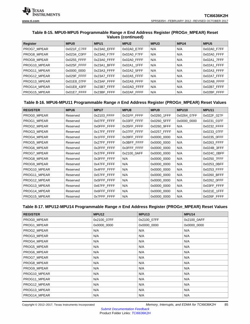
85
TCI6636K2Hwww.ti.com SPRS835H –FEBRUARY 2012–REVISED OCTOBER 2017
Submit Documentation FeedbackProduct Folder Links: TCI6636K2H
Memory, Interrupts, and EDMA for TCI6636K2HCopyright © 2012–2017, Texas Instruments Incorporated
Table 8-15. MPU0-MPU5 Programmable Range n End Address Register (PROGn_MPEAR) ResetValues (continued)
Register MPU0 MPU1 MPU2 MPU3 MPU4 MPU5PROG7_MPEAR 0x021F_C7FF 0x23A0_EFFF 0x02A0_E7FF N/A N/A 0x02A0_F7FFPROG8_MPEAR 0x0234_C0FF 0x23A0_F7FF 0x02A0_F7FF N/A N/A 0x02A0_FFFFPROG9_MPEAR 0x0255_FFFF 0x23A0_FFFF 0x02A0_FFFF N/A N/A 0x02A1_7FFFPROG10_MPEAR 0x025F_FFFF 0x23A1_BFFF 0x02A1_1FFF N/A N/A 0x02A1_FFFFPROG11_MPEAR 0x0000_0000 0x23A3_FFFF 0x02A2_5FFF N/A N/A 0x02A3_FFFFPROG12_MPEAR 0x029F_FFFF 0x23A7_FFFF 0x02A5_FFFF N/A N/A 0x02A7_FFFFPROG13_MPEAR 0x01E8_07FF 0x23AF_FFFF 0x02A9_FFFF N/A N/A 0x02AB_FFFFPROG14_MPEAR 0x01E8_43FF 0x23B7_FFFF 0x02AD_FFFF N/A N/A 0x02B7_FFFFPROG15_MPEAR 0x01E7_FFFF 0x23BF_FFFF 0x02AF_FFFF N/A N/A 0x02BF_FFFF
Table 8-16. MPU6-MPU11 Programmable Range n End Address Register (PROGn_MPEAR) Reset Values
REGISTER MPU6 MPU7 MPU8 MPU9 MPU10 MPU11PROG0_MPEAR Reserved 0x2103_FFFF 0x31FF_FFFF 0x0260_1FFF 0x0264_07FF 0x022F_027FPROG1_MPEAR Reserved 0x07FF_FFFF 0x33FF_FFFF 0x0260_5FFF 0x0000_0000 0x0231_01FFPROG2_MPEAR Reserved 0x0FFF_FFFF 0x35FF_FFFF 0x0260_9FFF N/A 0x0232_FFFFPROG3_MPEAR Reserved 0x17FF_FFFF 0x37FF_FFFF 0x0257_FFFF N/A 0x0233_07FFPROG4_MPEAR Reserved 0x1FFF_FFFF 0x39FF_FFFF 0x0000_0000 N/A 0x0235_0FFFPROG5_MPEAR Reserved 0x27FF_FFFF 0x3BFF_FFFF 0x0000_0000 N/A 0x0263_FFFFPROG6_MPEAR Reserved 0x2FFF_FFFF 0x3FFF_FFFF 0x0000_0000 N/A 0x024B_3FFFPROG7_MPEAR Reserved 0x37FF_FFFF 0x2100_0AFF 0x0000_0000 N/A 0x024C_0BFFPROG8_MPEAR Reserved 0x3FFF_FFFF N/A 0x0000_0000 N/A 0x0250_7FFFPROG9_MPEAR Reserved 0x47FF_FFFF N/A 0x0000_0000 N/A 0x0253_0BFFPROG10_MPEAR Reserved 0x4FFF_FFFF N/A 0x0000_0000 N/A 0x0253_FFFFPROG11_MPEAR Reserved 0x57FF_FFFF N/A 0x0000_0000 N/A 0x0260_BFFFPROG12_MPEAR Reserved 0x5FFF_FFFF N/A 0x0000_0000 N/A 0x0262_0FFFPROG13_MPEAR Reserved 0x67FF_FFFF N/A 0x0000_0000 N/A 0x03FF_FFFFPROG14_MPEAR Reserved 0x6FFF_FFFF N/A 0x0000_0000 N/A 0x021E_1FFFPROG15_MPEAR Reserved 0x7FFF_FFFF N/A 0x0000_0000 N/A 0x026F_FFFF
Table 8-17. MPU12-MPU14 Programmable Range n End Address Register (PROGn_MPEAR) Reset Values
REGISTER MPU12 MPU13 MPU14PROG0_MPEAR 0x2100_07FF 0x2100_07FF 0x2100_0AFFPROG1_MPEAR 0x0000_0000 0x0000_0000 0x0000_0000PROG2_MPEAR N/A N/A N/APROG3_MPEAR N/A N/A N/APROG4_MPEAR N/A N/A N/APROG5_MPEAR N/A N/A N/APROG6_MPEAR N/A N/A N/APROG7_MPEAR N/A N/A N/APROG8_MPEAR N/A N/A N/APROG9_MPEAR N/A N/A N/APROG10_MPEAR N/A N/A N/APROG11_MPEAR N/A N/A N/APROG12_MPEAR N/A N/A N/APROG13_MPEAR N/A N/A N/APROG14_MPEAR N/A N/A N/A

86
TCI6636K2HSPRS835H –FEBRUARY 2012–REVISED OCTOBER 2017 www.ti.com
Submit Documentation FeedbackProduct Folder Links: TCI6636K2H
Memory, Interrupts, and EDMA for TCI6636K2H Copyright © 2012–2017, Texas Instruments Incorporated
Table 8-17. MPU12-MPU14 Programmable Range n End Address Register (PROGn_MPEAR) ResetValues (continued)
REGISTER MPU12 MPU13 MPU14PROG15_MPEAR N/A N/A N/A
8.2.2.3 Programmable Range n Memory Protection Page Attribute Register (PROGn_MPPAR)
The programmable address memory protection page attribute register holds the permissions for theregion. This register is writeable only by a nondebug supervisor entity. If NS = 0 (secure mode) then theregister is also writeable only by a nondebug secure entity. The NS bit is writeable only by a nondebugsecure entity. For debug accesses, the register is writeable only when NS = 1 or EMU = 1. ThePROGn_MPPAR register is shown in Figure 8-4 and described in Table 8-18. The reset values are listedin Table 8-19 for MPU0-MPU5, Table 8-20 for MPU6-MPU11, and Table 8-21 for MPU12-MPU14.
Figure 8-4. Programmable Range n Memory Protection Page Attribute Register (PROGn_MPPAR)31 30 29 28 27 26 25 24 23 22 21 20 19 18 17 16
Reserved AID15 AID14 AID13 AID12 AID11 AID10 AID9 AID8 AID7 AID6
R R/W R/W R/W R/W R/W R/W R/W R/W R/W R/W
15 14 13 12 11 10 9 8 7 6 5 4 3 2 1 0
AID5 AID4 AID3 AID2 AID1 AID0 AIDX Rsvd NS EMU SR SW SX UR UW UX
R/W R/W R/W R/W R/W R/W R/W R R/W R/W R/W R/W R/W R/W R/W R/W
Table 8-18. Programmable Range n Memory Protection Page Attribute Register Field DescriptionsBits Name Description31-26 Reserved Reserved. Always read as 0.25 AID15 Controls access from ID = 15
• 0 = Access is not checked for permissions• 1 = Access is checked for permissions
24 AID14 Controls access from ID = 14• 0 = Access is not checked for permissions• 1 = Access is checked for permissions
23 AID13 Controls access from ID = 13• 0 = Access is not checked for permissions• 1 = Access is checked for permissions
22 AID12 Controls access from ID = 12• 0 = Access is not checked for permissions• 1 = Access is checked for permissions
21 AID11 Controls access from ID = 11• 0 = Access is not checked for permissions• 1 = Access is checked for permissions
20 AID10 Controls access from ID = 10• 0 = Access is not checked for permissions• 1 = Access is checked for permissions
19 AID9 Controls access from ID = 9• 0 = Access is not checked for permissions• 1 = Access is checked for permissions
18 AID8 Controls access from ID = 8• 0 = Access is not checked for permissions• 1 = Access is checked for permissions
17 AID7 Controls access from ID = 7• 0 = Access is not checked for permissions• 1 = Access is checked for permissions
16 AID6 Controls access from ID = 6• 0 = Access is not checked for permissions• 1 = Access is checked for permissions

87
TCI6636K2Hwww.ti.com SPRS835H –FEBRUARY 2012–REVISED OCTOBER 2017
Submit Documentation FeedbackProduct Folder Links: TCI6636K2H
Memory, Interrupts, and EDMA for TCI6636K2HCopyright © 2012–2017, Texas Instruments Incorporated
Table 8-18. Programmable Range n Memory Protection Page Attribute Register FieldDescriptions (continued)
Bits Name Description15 AID5 Controls access from ID = 5
• 0 = Access is not checked for permissions• 1 = Access is checked for permissions
14 AID4 Controls access from ID = 4• 0 = Access is not checked for permissions• 1 = Access is checked for permissions
13 AID3 Controls access from ID = 3• 0 = Access is not checked for permissions• 1 = Access is checked for permissions
12 AID2 Controls access from ID = 2• 0 = Access is not checked for permissions• 1 = Access is checked for permissions
11 AID1 Controls access from ID = 1• 0 = Access is not checked for permissions• 1 = Access is checked for permissions
10 AID0 Controls access from ID = 0• 0 = Access is not checked for permissions• 1 = Access is checked for permissions
9 AIDX Controls access from ID > 15• 0 = Access is not checked for permissions• 1 = Access is checked for permissions
8 Reserved Reserved. Always reads as 0.7 NS Nonsecure access permission
• 0 = Only secure access allowed• 1 = Nonsecure access allowed
6 EMU Emulation (debug) access permission. This bit is ignored if NS = 1• 0 = Debug access not allowed• 1 = Debug access allowed
5 SR Supervisor Read permission• 0 = Access not allowed• 1 = Access allowed
4 SW Supervisor Write permission• 0 = Access not allowed• 1 = Access allowed
3 SX Supervisor Execute permission• 0 = Access not allowed• 1 = Access allowed
2 UR User Read permission• 0 = Access not allowed• 1 = Access allowed
1 UW User Write permission• 0 = Access not allowed• 1 = Access allowed
0 UX User Execute permission• 0 = Access not allowed• 1 = Access allowed

88
TCI6636K2HSPRS835H –FEBRUARY 2012–REVISED OCTOBER 2017 www.ti.com
Submit Documentation FeedbackProduct Folder Links: TCI6636K2H
Memory, Interrupts, and EDMA for TCI6636K2H Copyright © 2012–2017, Texas Instruments Incorporated
Table 8-19. MPU0-MPU5 Programmable Range n Memory Protection Page Attribute Register(PROGn_MPPAR) Reset Values
REGISTER MPU0 MPU1 MPU2 MPU3 MPU4 MPU5PROG0_MPPAR 0x03FF_FCB6 0x03FF_FCB6 0x03FF_FCB6 0x03FF_FCB6 0x03FF_FCB6 0x03FF_FCB4PROG1_MPPAR 0x03FF_FCB6 0x03FF_FCB4 0x03FF_FCB4 0x03FF_FCB6 0x03FF_FCB6 0x03FF_FCB4PROG2_MPPAR 0x03FF_FCB6 0x03FF_FCA4 0x03FF_FCA4 N/A 0x03FF_FCB6 0x03FF_FCA4PROG3_MPPAR 0x03FF_FCB6 0x03FF_FCB4 0x03FF_FCB4 N/A 0x03FF_FCB6 0x03FF_FCF4PROG4_MPPAR 0x03FF_FCB6 0x03FF_FCF4 0x03FF_FCF4 N/A N/A 0x03FF_FCB4PROG5_MPPAR 0x03FF_FCB6 0x03FF_FCB4 0x03FF_FCB4 N/A N/A 0x03FF_FCB4PROG6_MPPAR 0x03FF_FCB6 0x03FF_FCB4 0x03FF_FCB4 N/A N/A 0x03FF_FCB4PROG7_MPPAR 0x03FF_FCB6 0x03FF_FCB4 0x03FF_FCB4 N/A N/A 0x03FF_FCB4PROG8_MPPAR 0x03FF_FCB6 0x03FF_FCB4 0x03FF_FCB4 N/A N/A 0x03FF_FCF4PROG9_MPPAR 0x03FF_FCB6 0x03FF_FCF4 0x03FF_FCF4 N/A N/A 0x03FF_FCB4PROG10_MPPAR 0x03FF_FCB6 0x03FF_FCB4 0x03FF_FCB4 N/A N/A 0x03FF_FCF4PROG11_MPPAR 0x03FF_FCB6 0x03FF_FCF4 0x03FF_FCF4 N/A N/A 0x03FF_FCF4PROG12_MPPAR 0x03FF_FCB4 0x03FF_FCA4 0x03FF_FCA4 N/A N/A 0x03FF_FCA4PROG13_MPPAR 0x03FF_FCB6 0x03FF_FCB6 0x03FF_FCB6 N/A N/A 0x03FF_FCB6PROG14_MPPAR 0x03FF_FCB0 0x03FF_FCA4 0x03FF_FCB6 N/A N/A 0x03FF_FCA4PROG15_MPPAR 0x03FF_FCB6 0x03FF_FCA4 0x03FF_FCB6 N/A N/A 0x03FF_FCA4
Table 8-20. MPU6-MPU11 Programmable Range n Memory Protection Page Attribute Register(PROGn_MPPAR) Reset Values
REGISTER MPU6 MPU7 MPU8 MPU9 MPU10 MPU11PROG0_MPPAR Reserved 0x03FF_FCB6 0x03FF_FCBF 0x03FF_FCB6 0x03FF_FCB6 0x03FF_FCB6PROG1_MPPAR Reserved 0x03FF_FCBF 0x03FF_FCBF 0x03FF_FCB6 0x03FF_FCB6 0x03FF_FCB0PROG2_MPPAR Reserved 0x03FF_FCBF 0x03FF_FCBF 0x03FF_FCB6 N/A 0x03FF_FCB6PROG3_MPPAR Reserved 0x03FF_FCBF 0x03FF_FCBF 0x03FF_FCB6 N/A 0x03FF_FCB0PROG4_MPPAR Reserved 0x03FF_FCBF 0x03FF_FCBF 0x03FF_FCB6 N/A 0x03FF_FCB0PROG5_MPPAR Reserved 0x03FF_FCBF 0x03FF_FCBF 0x03FF_FCB6 N/A 0x03FF_FCB6PROG6_MPPAR Reserved 0x03FF_FCBF 0x03FF_FCBF 0x03FF_FCB6 N/A 0x03FF_FCB6PROG7_MPPAR Reserved 0x03FF_FCBF 0x03FF_FCB6 0x03FF_FCB6 N/A 0x03FF_FCB0PROG8_MPPAR Reserved 0x03FF_FCBF N/A 0x03FF_FCB6 N/A 0x03FF_FCB0PROG9_MPPAR Reserved 0x03FF_FCBF N/A 0x03FF_FCB6 N/A 0x03FF_FCB6PROG10_MPPAR Reserved 0x03FF_FCBF N/A 0x03FF_FCB6 N/A 0x03FF_FCB6PROG11_MPPAR Reserved 0x03FF_FCBF N/A 0x03FF_FCB6 N/A 0x03FF_FCB6PROG12_MPPAR Reserved 0x03FF_FCBF N/A 0x03FF_FCB6 N/A 0x03FF_FCB0PROG13_MPPAR Reserved 0x03FF_FCBF N/A 0x03FF_FCB6 N/A 0x03FF_FCB6PROG14_MPPAR Reserved 0x03FF_FCBF N/A 0x03FF_FCB6 N/A 0x03FF_FCB0PROG15_MPPAR Reserved 0x03FF_FCBF N/A 0x03FF_FCB6 N/A 0x03FF_FCB6
Table 8-21. MPU12-MPU14 Programmable Range n Memory Protection Page Attribute Register(PROGn_MPPAR) Reset Values
Register MPU12 MPU13 MPU14PROG0_MPPAR 0x03FF_FCB6 0x03FF_FCB6 0x03FF_FCB6PROG1_MPPAR 0x03FF_FCBF 0x03FF_FCBF 0x03FF_FCBFPROG2_MPPAR Reserved Reserved ReservedPROG3_MPPAR N/A N/A N/APROG4_MPPAR N/A N/A N/APROG5_MPPAR N/A N/A N/A

89
TCI6636K2Hwww.ti.com SPRS835H –FEBRUARY 2012–REVISED OCTOBER 2017
Submit Documentation FeedbackProduct Folder Links: TCI6636K2H
Memory, Interrupts, and EDMA for TCI6636K2HCopyright © 2012–2017, Texas Instruments Incorporated
Table 8-21. MPU12-MPU14 Programmable Range n Memory Protection Page Attribute Register(PROGn_MPPAR) Reset Values (continued)
Register MPU12 MPU13 MPU14PROG6_MPPAR N/A N/A N/APROG7_MPPAR N/A N/A N/APROG8_MPPAR N/A N/A N/APROG9_MPPAR N/A N/A N/APROG10_MPPAR N/A N/A N/APROG11_MPPAR N/A N/A N/APROG12_MPPAR N/A N/A N/APROG13_MPPAR N/A N/A N/APROG14_MPPAR N/A N/A N/APROG15_MPPAR N/A N/A N/A
8.3 InterruptsThis section discusses the interrupt sources, controller, and topology. Also provided are tables describingthe interrupt events.
8.3.1 Interrupt Sources and Interrupt ControllerThe CPU interrupts on the TCI6636K2H device are configured through the C66x CorePac InterruptController. The Interrupt Controller allows for up to 128 system events to be programmed to any of the 12CPU interrupt inputs (CPUINT4 - CPUINT15), the CPU exception input (EXCEP), or the advancedemulation logic. The 128 system events consist of both internally-generated events (within the CorePac)and chip-level events.
Additional system events are routed to each of the C66x CorePacs to provide chip-level events that arenot required as CPU interrupts/exceptions to be routed to the Interrupt Controller as emulation events. Inaddition, error-class events or infrequently used events are also routed through the system event router tooffload the C66x CorePac interrupt selector. This is accomplished through the CorePac InterruptController blocks, CIC[2:0]. This is clocked using CPU/6.
The event controllers consist of simple combination logic to provide additional events to each C66xCorePac, ARM GIC (ARM Generic Interrupt Controller) plus the EDMA3CC. CIC0 has 104 event outputswhich provides 20 broadcast events and 18 additional events to each of the C66x CorePacs, 0 through 3.Similarly, CIC1 has 104 event outputs which provides 20 broadcast events and 18 additional events toeach of the C66x CorePacs, 4 through 7. CIC2 has 103 event outputs which provides 8, 20, 8, 8, 8, and16 events to EDMA3CC0, EDMA3CC1, EDMA3C2, EDMA3CC3, EDMA3CC4, and HyperLinksrespectively.
The events that are routed to the C66x CorePacs for Advanced Event Triggering (AET) purposes fromthose EDMA3CC and FSYNC events that are not otherwise provided to each C66x CorePac.
Modules such as FFTC, TCP3d, TAC, AIF, CP_MPU, BOOT_CFG, and CP_Tracer have level interruptsand EOI handshaking interface. The EOI value is 0 for TCP3d_x, TAC, AIF, CP_MPU, BOOT_CFG, andCP_Tracer.
For FFTC:• the EOI value is 0 for FFTC_x_INTD_INTR0,• the EOI value is 1 for FFTC_x_INTD_INTR1,• the EOI value is 2 for FFTC_x_INTD_INTR2• the EOI value is 3 for FFTC_x_INTD_INTR3 (where FFTC_x can be FFTC_0, FFTC_1, FFTC_2 or
FFTC_3)
Figure 8-5 shows the TCI6636K2H interrupt topology.

56 Primary Events
8 Secondary Events
357 Common Events
19 Reserved Events
EDMA3CC0
C66xCorePac7
18 Secondary Events
26 QMSS q_pend Events
402 Common Events
12 Reserved Events
24 Primary Events2×
8 2 Secondary Events×HyperLink
44 Primary Events
20 Secondary Events
EDMA3CC1
56 Primary Events
8 Secondary Events
EDMA3CC2
56 Primary Events
8 Secondary Events
EDMA3CC3
C66xCorePac6
18 Secondary Events
C66xCorePac5
18 Secondary Events
C66xCorePac4
18 Secondary Events
19 Unique Primary Events
20 Broadcast Events from CIC0
C66xCorePac3
18 Secondary Events
C66xCorePac2
18 Secondary Events
C66xCorePac1
18 Secondary Events
C66xCorePac0
18 Secondary Events
19 Unique Primary Events
19 Unique Primary Events
19 Unique Primary Events
19 Unique Primary Events
19 Unique Primary Events
19 Unique Primary Events
19 Unique Primary Events
20 Broadcast Events from CIC1
56 Primary Events
8 Secondary Events
EDMA3CC4
8 Broadcast Events from AIF2
57 Shared Primary Events
9 QMSS q_pend Events
32 QMSS lo Events
26 QMSS q_pend Events
402 Common Events
12 Reserved Events
9 QMSS q_pend Events
32 QMSS_lo Events
32 QMSS_2 hi Events
39 QMSS q_pend Events
32 QMSS_1 hi Events
6636-38
8 Shared Events
CIC1
CIC0
ARMINTC
480 SPI EventsPeripherals36
CIC2
90
TCI6636K2HSPRS835H –FEBRUARY 2012–REVISED OCTOBER 2017 www.ti.com
Submit Documentation FeedbackProduct Folder Links: TCI6636K2H
Memory, Interrupts, and EDMA for TCI6636K2H Copyright © 2012–2017, Texas Instruments Incorporated
Figure 8-5. Interrupt Topology
Table 8-22 shows the mapping of primary events to C66x Corepac.

91
TCI6636K2Hwww.ti.com SPRS835H –FEBRUARY 2012–REVISED OCTOBER 2017
Submit Documentation FeedbackProduct Folder Links: TCI6636K2H
Memory, Interrupts, and EDMA for TCI6636K2HCopyright © 2012–2017, Texas Instruments Incorporated
(1) For C66x CorePac[0-3], this generic primary interrupt comes from CIC0 and for C66x CorePac[4-7], this generic primary interrupt comesfrom CIC1.
(2) N = core number.
Table 8-22. System Event Mapping — C66x CorePac Primary Interrupts
EVENT NO. EVENT NAME DESCRIPTION0 EVT0 Event combiner 0 output1 EVT1 Event combiner 1 output2 EVT2 Event combiner 2 output3 EVT3 Event combiner 3 output4 TETB_HFULLINTN TETB is half full5 TETB_FULLINTN TETB is full6 TETB_ACQINTN TETB Acquisition complete interrupt7 TETB_OVFLINTN TETB Overflow condition interrupt8 TETB_UNFLINTN TETB Underflow condition interrupt9 EMU_DTDMA Emulation interrupt for host scan, DTDMA transfer complete and
AET10 MSMC_MPF_ERRORN Memory protection fault indicators for system master PrivID = 0
(C66x CorePac)11 EMU_RTDXRX Reserved12 EMU_RTDXTX Reserved13 IDMA0 IDMA channel 0 interrupt14 IDMA1 IDMA channel 1 interrupt15 SEM_ERRN Semaphore error interrupt16 SEM_INTN Semaphore interrupt17 PCIE_INT4_PLUS_N PCIE0 MSI interrupt18 Reserved Reserved19 RAC_0_INT RAC interrupt20 SRIO_INTDST16_PLUS_N SRIO interrupt21 Reserved Reserved22 RAC_1_INT RAC interrupt23 CIC_OUT35 CIC Interrupt Controller output (1)
24 CIC_2_OUT102 CIC Interrupt Controller output25 CIC_2_OUT94_PLUS_N (2) CIC Interrupt Controller output26 CIC_OUT68_PLUS_10_MUL_N (2) CIC Interrupt Controller output (1)
27 CIC_OUT69_PLUS_10_MUL_N (2) CIC Interrupt Controller output (1)
28 CIC_OUT70_PLUS_10_MUL_N (2) CIC Interrupt Controller output (1)
29 CIC_OUT71_PLUS_10_MUL_N (2) CIC Interrupt Controller output (1)
30 CIC_OUT72_PLUS_10_MUL_N (2) CIC Interrupt Controller output (1)
31 CIC_OUT73_PLUS_10_MUL_N (2) CIC Interrupt Controller output (1)
32 CIC_OUT16 CIC Interrupt Controller output (1)
33 CIC_OUT17 CIC Interrupt Controller output (1)
34 CIC_OUT18 CIC Interrupt Controller output (1)
35 CIC_OUT19 CIC Interrupt Controller output (1)
36 CIC_OUT20 CIC Interrupt Controller output (1)
37 CIC_OUT21 CIC Interrupt Controller output (1)
38 CIC_OUT22 CIC Interrupt Controller output (1)
39 CIC_OUT23 CIC Interrupt Controller output (1)
40 CIC_OUT32 CIC Interrupt Controller output (1)
41 CIC_OUT33 CIC Interrupt Controller output (1)
42 CIC_OUT13_PLUS_16_MUL_N (2) CIC Interrupt Controller output (1)
43 CIC_OUT14_PLUS_16_MUL_N (2) CIC Interrupt Controller output (1)

92
TCI6636K2HSPRS835H –FEBRUARY 2012–REVISED OCTOBER 2017 www.ti.com
Submit Documentation FeedbackProduct Folder Links: TCI6636K2H
Memory, Interrupts, and EDMA for TCI6636K2H Copyright © 2012–2017, Texas Instruments Incorporated
Table 8-22. System Event Mapping — C66x CorePac Primary Interrupts (continued)EVENT NO. EVENT NAME DESCRIPTION44 CIC_OUT15_PLUS_16_MUL_N (2) CIC Interrupt Controller output (1)
45 CIC_OUT64_PLUS_10_MUL_N (2) CIC Interrupt Controller output (1)
46 CIC_OUT65_PLUS_10_MUL_N (2) CIC Interrupt Controller output (1)
47 CIC_OUT66_PLUS_10_MUL_N (2) CIC Interrupt Controller output (1)
48 QMSS_INTD_1_HIGH_N (2) Navigator 1 accumulated hi-priority interrupt 049 QMSS_INTD_1_HIGH_8_PLUS_N (2) Navigator 1 accumulated hi-priority interrupt 850 QMSS_INTD_1_HIGH_16_PLUS_N (2) Navigator 1 accumulated hi-priority interrupt 1651 QMSS_INTD_1_HIGH_24_PLUS_N (2) Navigator 1 accumulated hi-priority interrupt 2452 QMSS_INTD_2_HIGH_N (2) Navigator 2 accumulated hi-priority interrupt 053 QMSS_INTD_2_HIGH_8_PLUS_N (2) Navigator 2 accumulated hi-priority interrupt 854 QMSS_INTD_2_HIGH_16_PLUS_N (2) Navigator 2 accumulated hi-priority interrupt 1655 QMSS_INTD_2_HIGH_24_PLUS_N (2) Navigator 2 accumulated hi-priority interrupt 2456 CIC_OUT0 CIC Interrupt Controller output (1)
57 CIC_OUT1 CIC Interrupt Controller output (1)
58 CIC_OUT2 CIC Interrupt Controller output (1)
59 CIC_OUT3 CIC Interrupt Controller output (1)
60 CIC_OUT4 CIC Interrupt Controller output (1)
61 CIC_OUT5 CIC Interrupt Controller output (1)
62 CIC_OUT6 CIC Interrupt Controller output (1)
63 CIC_OUT7 CIC Interrupt Controller output (1)
64 TIMER_N_INTL Local timer interrupt low65 TIMER_N_INTH Local timer interrupt high66 TIMER_8_INTL Timer interrupt low67 TIMER_8_INTH Timer interrupt high68 TIMER_9_INTL Timer interrupt low69 TIMER_9_INTH Timer interrupt high70 TIMER_10_INTL Timer interrupt low71 TIMER_10_INTH Timer interrupt high72 TIMER_11_INTL Timer interrupt low73 TIMER_11_INTH Timer interrupt high74 CIC_OUT8_PLUS_16_MUL_N (2) CIC Interrupt Controller output (1)
75 CIC_OUT9_PLUS_16_MUL_N (2) CIC Interrupt Controller output (1)
76 CIC_OUT10_PLUS_16_MUL_N (2) CIC Interrupt Controller output (1)
77 CIC_OUT11_PLUS_16_MUL_N (2) CIC Interrupt Controller output (1)
78 TIMER_14_INTL Timer interrupt low79 TIMER_14_INTH Timer interrupt high80 TIMER_15_INTL Timer interrupt low81 TIMER_15_INTH Timer interrupt high82 GPIO_INT8 Local GPIO interrupt83 GPIO_INT9 Local GPIO interrupt84 GPIO_INT10 Local GPIO interrupt85 GPIO_INT11 Local GPIO interrupt86 GPIO_INT12 Local GPIO interrupt87 AIF_ATEVT0 AIF Timer event88 AIF_ATEVT1 AIF Timer event89 AIF_ATEVT2 AIF Timer event90 AIF_ATEVT3 AIF Timer event

93
TCI6636K2Hwww.ti.com SPRS835H –FEBRUARY 2012–REVISED OCTOBER 2017
Submit Documentation FeedbackProduct Folder Links: TCI6636K2H
Memory, Interrupts, and EDMA for TCI6636K2HCopyright © 2012–2017, Texas Instruments Incorporated
Table 8-22. System Event Mapping — C66x CorePac Primary Interrupts (continued)EVENT NO. EVENT NAME DESCRIPTION91 AIF_ATEVT4 AIF Timer event92 AIF_ATEVT5 AIF Timer event93 AIF_ATEVT6 AIF Timer event94 AIF_ATEVT7 AIF Timer event95 CIC_OUT67_PLUS_10_MUL_N (2) CIC Interrupt Controller output (1)
96 INTERR Dropped C66x CorePac interrupt event97 EMC_IDMAERR Invalid IDMA parameters98 Reserved Reserved99 CIC_2_SPECIAL_BROADCAST CIC Interrupt Controller output100 EFIINT0 EFI interrupt from Side A101 EFIINT1 EFI interrupt from Side B102 GPIO_INT13 Local GPIO interrupt103 GPIO_INT14 Local GPIO interrupt104 GPIO_INT15 Local GPIO interrupt105 IPC_GRN Boot CFG106 GPIO_INTN GPIO interrupt107 CIC_OUT12_PLUS_16_MUL_N (2) CIC Interrupt Controller output (1)
108 CIC_OUT34 CIC Interrupt Controller output (1)
109 CIC_2_OUT13 CIC Interrupt Controller output110 MDMAERREVT DMA internal bus error event111 Reserved Reserved112 EDMACC_0_4_TC_AET_INT EDMA3CC0_4 AET event113 PMC_ED Single bit error detected during DMA read114 EDMACC_1_2_TC_AET_INT EDMA3CC1_2 AET event115 EDMACC_1_3_TC_AET_INT EDMA3CC3_4 AET event116 UMC_ED1 Corrected bit error detected117 UMC_ED2 Uncorrected bit error detected118 PDC_INT Power down sleep interrupt119 SYS_CMPA SYS CPU MP fault event120 PMC_CMPA CPU memory protection fault121 PMC_DMPA DMA memory protection fault122 DMC_CMPA CPU memory protection fault123 DMC_DMPA DMA memory protection fault124 UMC_CMPA CPU memory protection fault125 UMC_DMPA DMA memory protection fault126 EMC_CMPA CPU memory protection fault127 EMC_BUSERR Bus error interrupt
Table 8-23 lists the ARM CorePac interrupt inputs.
NOTEEvent No. 0 is identical to ARM GIC interrupt ID 0.
Table 8-23. System Event Mapping — ARM CorePac Interrupts
EVENT NO. EVENT NAME DESCRIPTION0 RSTMUX_INT8 Boot config watchdog timer expiration (timer 16) event for ARM
Core 0
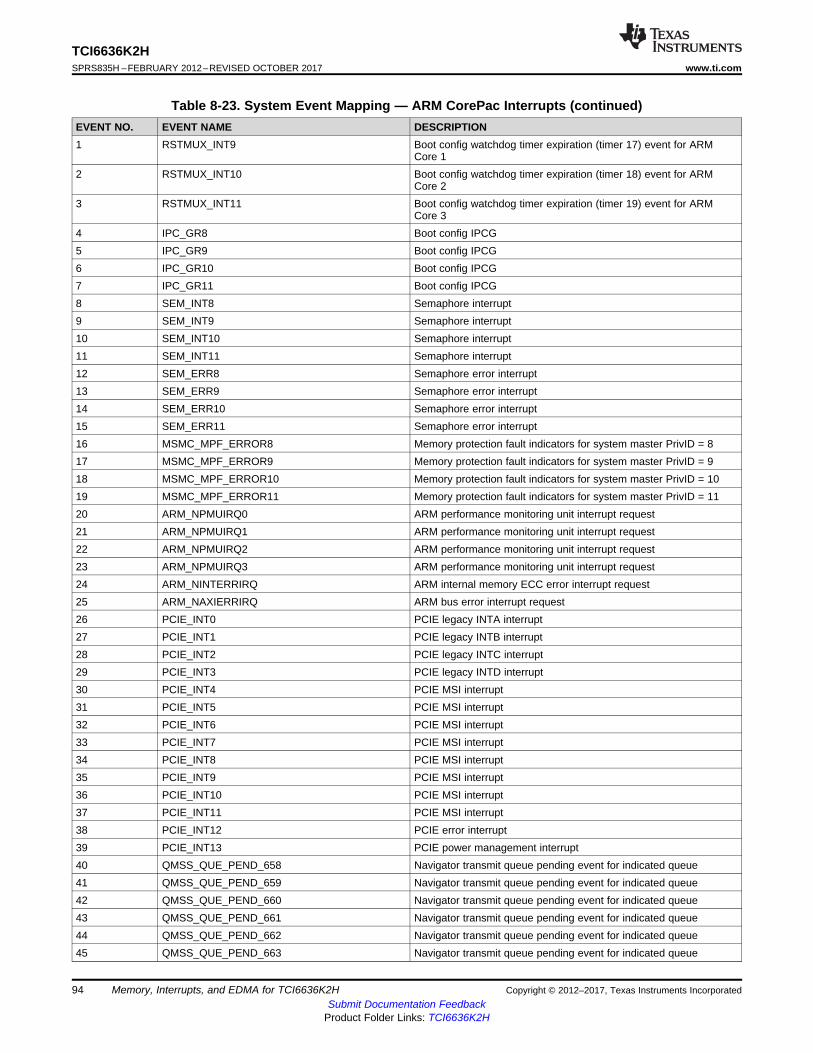
94
TCI6636K2HSPRS835H –FEBRUARY 2012–REVISED OCTOBER 2017 www.ti.com
Submit Documentation FeedbackProduct Folder Links: TCI6636K2H
Memory, Interrupts, and EDMA for TCI6636K2H Copyright © 2012–2017, Texas Instruments Incorporated
Table 8-23. System Event Mapping — ARM CorePac Interrupts (continued)EVENT NO. EVENT NAME DESCRIPTION1 RSTMUX_INT9 Boot config watchdog timer expiration (timer 17) event for ARM
Core 12 RSTMUX_INT10 Boot config watchdog timer expiration (timer 18) event for ARM
Core 23 RSTMUX_INT11 Boot config watchdog timer expiration (timer 19) event for ARM
Core 34 IPC_GR8 Boot config IPCG5 IPC_GR9 Boot config IPCG6 IPC_GR10 Boot config IPCG7 IPC_GR11 Boot config IPCG8 SEM_INT8 Semaphore interrupt9 SEM_INT9 Semaphore interrupt10 SEM_INT10 Semaphore interrupt11 SEM_INT11 Semaphore interrupt12 SEM_ERR8 Semaphore error interrupt13 SEM_ERR9 Semaphore error interrupt14 SEM_ERR10 Semaphore error interrupt15 SEM_ERR11 Semaphore error interrupt16 MSMC_MPF_ERROR8 Memory protection fault indicators for system master PrivID = 817 MSMC_MPF_ERROR9 Memory protection fault indicators for system master PrivID = 918 MSMC_MPF_ERROR10 Memory protection fault indicators for system master PrivID = 1019 MSMC_MPF_ERROR11 Memory protection fault indicators for system master PrivID = 1120 ARM_NPMUIRQ0 ARM performance monitoring unit interrupt request21 ARM_NPMUIRQ1 ARM performance monitoring unit interrupt request22 ARM_NPMUIRQ2 ARM performance monitoring unit interrupt request23 ARM_NPMUIRQ3 ARM performance monitoring unit interrupt request24 ARM_NINTERRIRQ ARM internal memory ECC error interrupt request25 ARM_NAXIERRIRQ ARM bus error interrupt request26 PCIE_INT0 PCIE legacy INTA interrupt27 PCIE_INT1 PCIE legacy INTB interrupt28 PCIE_INT2 PCIE legacy INTC interrupt29 PCIE_INT3 PCIE legacy INTD interrupt30 PCIE_INT4 PCIE MSI interrupt31 PCIE_INT5 PCIE MSI interrupt32 PCIE_INT6 PCIE MSI interrupt33 PCIE_INT7 PCIE MSI interrupt34 PCIE_INT8 PCIE MSI interrupt35 PCIE_INT9 PCIE MSI interrupt36 PCIE_INT10 PCIE MSI interrupt37 PCIE_INT11 PCIE MSI interrupt38 PCIE_INT12 PCIE error interrupt39 PCIE_INT13 PCIE power management interrupt40 QMSS_QUE_PEND_658 Navigator transmit queue pending event for indicated queue41 QMSS_QUE_PEND_659 Navigator transmit queue pending event for indicated queue42 QMSS_QUE_PEND_660 Navigator transmit queue pending event for indicated queue43 QMSS_QUE_PEND_661 Navigator transmit queue pending event for indicated queue44 QMSS_QUE_PEND_662 Navigator transmit queue pending event for indicated queue45 QMSS_QUE_PEND_663 Navigator transmit queue pending event for indicated queue

95
TCI6636K2Hwww.ti.com SPRS835H –FEBRUARY 2012–REVISED OCTOBER 2017
Submit Documentation FeedbackProduct Folder Links: TCI6636K2H
Memory, Interrupts, and EDMA for TCI6636K2HCopyright © 2012–2017, Texas Instruments Incorporated
Table 8-23. System Event Mapping — ARM CorePac Interrupts (continued)EVENT NO. EVENT NAME DESCRIPTION46 QMSS_QUE_PEND_664 Navigator transmit queue pending event for indicated queue47 QMSS_QUE_PEND_665 Navigator transmit queue pending event for indicated queue48 QMSS_QUE_PEND_8704 Navigator transmit queue pending event for indicated queue49 QMSS_QUE_PEND_8705 Navigator transmit queue pending event for indicated queue50 QMSS_QUE_PEND_8706 Navigator transmit queue pending event for indicated queue51 QMSS_QUE_PEND_8707 Navigator transmit queue pending event for indicated queue52 QMSS_QUE_PEND_8708 Navigator transmit queue pending event for indicated queue53 QMSS_QUE_PEND_8709 Navigator transmit queue pending event for indicated queue54 QMSS_QUE_PEND_8710 Navigator transmit queue pending event for indicated queue55 QMSS_QUE_PEND_8711 Navigator transmit queue pending event for indicated queue56 QMSS_QUE_PEND_8712 Navigator transmit queue pending event for indicated queue57 QMSS_QUE_PEND_8713 Navigator transmit queue pending event for indicated queue58 QMSS_QUE_PEND_8714 Navigator transmit queue pending event for indicated queue59 QMSS_QUE_PEND_8715 Navigator transmit queue pending event for indicated queue60 QMSS_QUE_PEND_8716 Navigator transmit queue pending event for indicated queue61 QMSS_QUE_PEND_8717 Navigator transmit queue pending event for indicated queue62 QMSS_QUE_PEND_8718 Navigator transmit queue pending event for indicated queue63 QMSS_QUE_PEND_8719 Navigator transmit queue pending event for indicated queue64 QMSS_QUE_PEND_8720 Navigator transmit queue pending event for indicated queue65 QMSS_QUE_PEND_8721 Navigator transmit queue pending event for indicated queue66 QMSS_QUE_PEND_8722 Navigator transmit queue pending event for indicated queue67 QMSS_QUE_PEND_8723 Navigator transmit queue pending event for indicated queue68 QMSS_QUE_PEND_8724 Navigator transmit queue pending event for indicated queue69 QMSS_QUE_PEND_8725 Navigator transmit queue pending event for indicated queue70 QMSS_QUE_PEND_8726 Navigator transmit queue pending event for indicated queue71 QMSS_QUE_PEND_8727 Navigator transmit queue pending event for indicated queue72 QMSS_QUE_PEND_8728 Navigator transmit queue pending event for indicated queue73 QMSS_QUE_PEND_8729 Navigator transmit queue pending event for indicated queue74 QMSS_QUE_PEND_8730 Navigator transmit queue pending event for indicated queue75 QMSS_QUE_PEND_8731 Navigator transmit queue pending event for indicated queue76 QMSS_QUE_PEND_8732 Navigator transmit queue pending event for indicated queue77 QMSS_QUE_PEND_8733 Navigator transmit queue pending event for indicated queue78 QMSS_QUE_PEND_8734 Navigator transmit queue pending event for indicated queue79 QMSS_QUE_PEND_8735 Navigator transmit queue pending event for indicated queue80 TIMER_0_INTL Timer interrupt low81 TIMER_0_INTH Timer interrupt high82 TIMER_1_INTL Timer interrupt low83 TIMER_1_INTH Timer interrupt high84 TIMER_2_INTL Timer interrupt low85 TIMER_2_INTH Timer interrupt high86 TIMER_3_INTL Timer interrupt low87 TIMER_3_INTH Timer interrupt high88 TIMER_4_INTL Timer interrupt low89 TIMER_4_INTH Timer interrupt high90 TIMER_5_INTL Timer interrupt low91 TIMER_5_INTH Timer interrupt high92 TIMER_6_INTL Timer interrupt low

96
TCI6636K2HSPRS835H –FEBRUARY 2012–REVISED OCTOBER 2017 www.ti.com
Submit Documentation FeedbackProduct Folder Links: TCI6636K2H
Memory, Interrupts, and EDMA for TCI6636K2H Copyright © 2012–2017, Texas Instruments Incorporated
Table 8-23. System Event Mapping — ARM CorePac Interrupts (continued)EVENT NO. EVENT NAME DESCRIPTION93 TIMER_6_INTH Timer interrupt high94 TIMER_7_INTL Timer interrupt low95 TIMER_7_INTH Timer interrupt high96 TIMER_8_INTL Timer interrupt low97 TIMER_8_INTH Timer interrupt high98 TIMER_9_INTL Timer interrupt low99 TIMER_9_INTH Timer interrupt high100 TIMER_10_INTL Timer interrupt low101 TIMER_10_INTH Timer interrupt high102 TIMER_11_INTL Timer interrupt low103 TIMER_11_INTH Timer interrupt high104 TIMER_12_INTL Timer interrupt low105 TIMER_12_INTH Timer interrupt high106 TIMER_13_INTL Timer interrupt low107 TIMER_13_INTH Timer interrupt high108 TIMER_14_INTL Timer interrupt low109 TIMER_14_INTH Timer interrupt high110 TIMER_15_INTL Timer interrupt low111 TIMER_15_INTH Timer interrupt high112 TIMER_16_INTL Timer interrupt low113 TIMER_16_INTH Timer interrupt high114 TIMER_17_INTL Timer interrupt low115 TIMER_17_INTH Timer interrupt high116 TIMER_18_INTL Timer interrupt low117 TIMER_18_INTH Timer interrupt high118 TIMER_19_INTL Timer interrupt low119 TIMER_19_INTH Timer interrupt high120 GPIO_INT0 GPIO interrupt121 GPIO_INT1 GPIO interrupt122 GPIO_INT2 GPIO interrupt123 GPIO_INT3 GPIO interrupt124 GPIO_INT4 GPIO interrupt125 GPIO_INT5 GPIO interrupt126 GPIO_INT6 GPIO interrupt127 GPIO_INT7 GPIO interrupt128 GPIO_INT8 GPIO interrupt129 GPIO_INT9 GPIO interrupt130 GPIO_INT10 GPIO interrupt131 GPIO_INT11 GPIO interrupt132 GPIO_INT12 GPIO interrupt133 GPIO_INT13 GPIO interrupt134 GPIO_INT14 GPIO interrupt135 GPIO_INT15 GPIO interrupt136 GPIO_INT16 GPIO interrupt137 GPIO_INT17 GPIO interrupt138 GPIO_INT18 GPIO interrupt139 GPIO_INT19 GPIO interrupt

97
TCI6636K2Hwww.ti.com SPRS835H –FEBRUARY 2012–REVISED OCTOBER 2017
Submit Documentation FeedbackProduct Folder Links: TCI6636K2H
Memory, Interrupts, and EDMA for TCI6636K2HCopyright © 2012–2017, Texas Instruments Incorporated
Table 8-23. System Event Mapping — ARM CorePac Interrupts (continued)EVENT NO. EVENT NAME DESCRIPTION140 GPIO_INT20 GPIO interrupt141 GPIO_INT21 GPIO interrupt142 GPIO_INT22 GPIO interrupt143 GPIO_INT23 GPIO interrupt144 GPIO_INT24 GPIO interrupt145 GPIO_INT25 GPIO interrupt146 GPIO_INT26 GPIO interrupt147 GPIO_INT27 GPIO interrupt148 GPIO_INT28 GPIO interrupt149 GPIO_INT29 GPIO interrupt150 GPIO_INT30 GPIO interrupt151 GPIO_INT31 GPIO interrupt152 SRIO_INT00 SRIO interrupt153 SRIO_INT01 SRIO interrupt154 SRIO_INT02 SRIO interrupt155 SRIO_INT03 SRIO interrupt156 SRIO_INT04 SRIO interrupt157 SRIO_INT05 SRIO interrupt158 SRIO_INT06 SRIO interrupt159 SRIO_INT07 SRIO interrupt160 SRIO_INT08 SRIO interrupt161 SRIO_INT09 SRIO interrupt162 SRIO_INT10 SRIO interrupt163 SRIO_INT11 SRIO interrupt164 SRIO_INT12 SRIO interrupt165 SRIO_INT13 SRIO interrupt166 SRIO_INT14 SRIO interrupt167 SRIO_INT15 SRIO interrupt168 SRIO_INT16 SRIO interrupt169 SRIO_INT17 SRIO interrupt170 SRIO_INT18 SRIO interrupt171 SRIO_INT19 SRIO interrupt172 SRIO_INT20 SRIO interrupt173 SRIO_INT21 SRIO interrupt174 SRIO_INT22 SRIO interrupt175 SRIO_INT23 SRIO interrupt176 SRIO_INT_PKTDMA_0 SRIO interrupt for Packet DMA starvation177 QMSS_INTD_1_PKTDMA_0 Navigator interrupt for Packet DMA starvation178 QMSS_INTD_1_PKTDMA_1 Navigator interrupt for Packet DMA starvation179 QMSS_INTD_1_HIGH_0 Navigator hi interrupt180 QMSS_INTD_1_HIGH_1 Navigator hi interrupt181 QMSS_INTD_1_HIGH_2 Navigator hi interrupt182 QMSS_INTD_1_HIGH_3 Navigator hi interrupt183 QMSS_INTD_1_HIGH_4 Navigator hi interrupt184 QMSS_INTD_1_HIGH_5 Navigator hi interrupt185 QMSS_INTD_1_HIGH_6 Navigator hi interrupt186 QMSS_INTD_1_HIGH_7 Navigator hi interrupt

98
TCI6636K2HSPRS835H –FEBRUARY 2012–REVISED OCTOBER 2017 www.ti.com
Submit Documentation FeedbackProduct Folder Links: TCI6636K2H
Memory, Interrupts, and EDMA for TCI6636K2H Copyright © 2012–2017, Texas Instruments Incorporated
Table 8-23. System Event Mapping — ARM CorePac Interrupts (continued)EVENT NO. EVENT NAME DESCRIPTION187 QMSS_INTD_1_HIGH_8 Navigator hi interrupt188 QMSS_INTD_1_HIGH_9 Navigator hi interrupt189 QMSS_INTD_1_HIGH_10 Navigator hi interrupt190 QMSS_INTD_1_HIGH_11 Navigator hi interrupt191 QMSS_INTD_1_HIGH_12 Navigator hi interrupt192 QMSS_INTD_1_HIGH_13 Navigator hi interrupt193 QMSS_INTD_1_HIGH_14 Navigator hi interrupt194 QMSS_INTD_1_HIGH_15 Navigator hi interrupt195 QMSS_INTD_1_HIGH_16 Navigator hi interrupt196 QMSS_INTD_1_HIGH_17 Navigator hi interrupt197 QMSS_INTD_1_HIGH_18 Navigator hi interrupt198 QMSS_INTD_1_HIGH_19 Navigator hi interrupt199 QMSS_INTD_1_HIGH_20 Navigator hi interrupt200 QMSS_INTD_1_HIGH_21 Navigator hi interrupt201 QMSS_INTD_1_HIGH_22 Navigator hi interrupt202 QMSS_INTD_1_HIGH_23 Navigator hi interrupt203 QMSS_INTD_1_HIGH_24 Navigator hi interrupt204 QMSS_INTD_1_HIGH_25 Navigator hi interrupt205 QMSS_INTD_1_HIGH_26 Navigator hi interrupt206 QMSS_INTD_1_HIGH_27 Navigator hi interrupt207 QMSS_INTD_1_HIGH_28 Navigator hi interrupt208 QMSS_INTD_1_HIGH_29 Navigator hi interrupt209 QMSS_INTD_1_HIGH_30 Navigator hi interrupt210 QMSS_INTD_1_HIGH_31 Navigator hi interrupt211 QMSS_INTD_1_LOW_0 Navigator interrupt212 QMSS_INTD_1_LOW_1 Navigator interrupt213 QMSS_INTD_1_LOW_2 Navigator interrupt214 QMSS_INTD_1_LOW_3 Navigator interrupt215 QMSS_INTD_1_LOW_4 Navigator interrupt216 QMSS_INTD_1_LOW_5 Navigator interrupt217 QMSS_INTD_1_LOW_6 Navigator interrupt218 QMSS_INTD_1_LOW_7 Navigator interrupt219 QMSS_INTD_1_LOW_8 Navigator interrupt220 QMSS_INTD_1_LOW_9 Navigator interrupt221 QMSS_INTD_1_LOW_10 Navigator interrupt222 QMSS_INTD_1_LOW_11 Navigator interrupt223 QMSS_INTD_1_LOW_12 Navigator interrupt224 QMSS_INTD_1_LOW_13 Navigator interrupt225 QMSS_INTD_1_LOW_14 Navigator interrupt226 QMSS_INTD_1_LOW_15 Navigator interrupt227 QMSS_INTD_2_PKTDMA_0 Navigator interrupt for Packet DMA starvation228 QMSS_INTD_2_PKTDMA_1 Navigator interrupt for Packet DMA starvation229 QMSS_INTD_2_HIGH_0 Navigator second hi interrupt230 QMSS_INTD_2_HIGH_1 Navigator second hi interrupt231 QMSS_INTD_2_HIGH_2 Navigator second hi interrupt232 QMSS_INTD_2_HIGH_3 Navigator second hi interrupt233 QMSS_INTD_2_HIGH_4 Navigator second hi interrupt

99
TCI6636K2Hwww.ti.com SPRS835H –FEBRUARY 2012–REVISED OCTOBER 2017
Submit Documentation FeedbackProduct Folder Links: TCI6636K2H
Memory, Interrupts, and EDMA for TCI6636K2HCopyright © 2012–2017, Texas Instruments Incorporated
Table 8-23. System Event Mapping — ARM CorePac Interrupts (continued)EVENT NO. EVENT NAME DESCRIPTION234 QMSS_INTD_2_HIGH_5 Navigator second hi interrupt235 QMSS_INTD_2_HIGH_6 Navigator second hi interrupt236 QMSS_INTD_2_HIGH_7 Navigator second hi interrupt237 QMSS_INTD_2_HIGH_8 Navigator second hi interrupt238 QMSS_INTD_2_HIGH_9 Navigator second hi interrupt239 QMSS_INTD_2_HIGH_10 Navigator second hi interrupt240 QMSS_INTD_2_HIGH_11 Navigator second hi interrupt241 QMSS_INTD_2_HIGH_12 Navigator second hi interrupt242 QMSS_INTD_2_HIGH_13 Navigator second hi interrupt243 QMSS_INTD_2_HIGH_14 Navigator second hi interrupt244 QMSS_INTD_2_HIGH_15 Navigator second hi interrupt245 QMSS_INTD_2_HIGH_16 Navigator second hi interrupt246 QMSS_INTD_2_HIGH_17 Navigator second hi interrupt247 QMSS_INTD_2_HIGH_18 Navigator second hi interrupt248 QMSS_INTD_2_HIGH_19 Navigator second hi interrupt249 QMSS_INTD_2_HIGH_20 Navigator second hi interrupt250 QMSS_INTD_2_HIGH_21 Navigator second hi interrupt251 QMSS_INTD_2_HIGH_22 Navigator second hi interrupt252 QMSS_INTD_2_HIGH_23 Navigator second hi interrupt253 QMSS_INTD_2_HIGH_24 Navigator second hi interrupt254 QMSS_INTD_2_HIGH_25 Navigator second hi interrupt255 QMSS_INTD_2_HIGH_26 Navigator second hi interrupt256 QMSS_INTD_2_HIGH_27 Navigator second hi interrupt257 QMSS_INTD_2_HIGH_28 Navigator second hi interrupt258 QMSS_INTD_2_HIGH_29 Navigator second hi interrupt259 QMSS_INTD_2_HIGH_30 Navigator second hi interrupt260 QMSS_INTD_2_HIGH_31 Navigator second hi interrupt261 QMSS_INTD_2_LOW_0 Navigator second interrupt262 QMSS_INTD_2_LOW_1 Navigator second interrupt263 QMSS_INTD_2_LOW_2 Navigator second interrupt264 QMSS_INTD_2_LOW_3 Navigator second interrupt265 QMSS_INTD_2_LOW_4 Navigator second interrupt266 QMSS_INTD_2_LOW_5 Navigator second interrupt267 QMSS_INTD_2_LOW_6 Navigator second interrupt268 QMSS_INTD_2_LOW_7 Navigator second interrupt269 QMSS_INTD_2_LOW_8 Navigator second interrupt270 QMSS_INTD_2_LOW_9 Navigator second interrupt271 QMSS_INTD_2_LOW_10 Navigator second interrupt272 QMSS_INTD_2_LOW_11 Navigator second interrupt273 QMSS_INTD_2_LOW_12 Navigator second interrupt274 QMSS_INTD_2_LOW_13 Navigator second interrupt275 QMSS_INTD_2_LOW_14 Navigator second interrupt276 QMSS_INTD_2_LOW_15 Navigator second interrupt277 UART_0_UARTINT UART0 interrupt278 UART_0_URXEVT UART0 receive event279 UART_0_UTXEVT UART0 transmit event280 UART_1_UARTINT UART1 interrupt

100
TCI6636K2HSPRS835H –FEBRUARY 2012–REVISED OCTOBER 2017 www.ti.com
Submit Documentation FeedbackProduct Folder Links: TCI6636K2H
Memory, Interrupts, and EDMA for TCI6636K2H Copyright © 2012–2017, Texas Instruments Incorporated
Table 8-23. System Event Mapping — ARM CorePac Interrupts (continued)EVENT NO. EVENT NAME DESCRIPTION281 UART_1_URXEVT UART1 receive event282 UART_1_UTXEVT UART1 transmit event283 I2C_0_INT I2C interrupt284 I2C_0_REVT I2C receive event285 I2C_0_XEVT I2C transmit event286 I2C_1_INT I2C interrupt287 I2C_1_REVT I2C receive event288 I2C_1_XEVT I2C transmit event289 I2C_2_INT I2C interrupt290 I2C_2_REVT I2C receive event291 I2C_2_XEVT I2C transmit event292 SPI_0_INT0 SPI interrupt293 SPI_0_INT1 SPI interrupt294 SPI_0_XEVT SPI DMA TX event295 SPI_0_REVT SPI DMA RX event296 SPI_1_INT0 SPI interrupt297 SPI_1_INT1 SPI interrupt298 SPI_1_XEVT SPI DMA TX event299 SPI_1_REVT SPI DMA RX event300 SPI_2_INT0 SPI interrupt301 SPI_2_INT1 SPI interrupt302 SPI_2_XEVT SPI DMA TX event303 SPI_2_REVT SPI DMA RX event304 DBGTBR_DMAINT Debug trace buffer (TBR) DMA event305 DBGTBR_ACQCOMP Debug trace buffer (TBR) Acquisition has been completed306 ARM_TBR_DMA ARM trace buffer (TBR) DMA event307 ARM_TBR_ACQ ARM trace buffer (TBR) Acquisition has been completed308 NETCP_MDIO_LINK_INT0 Packet Accelerator subsystem MDIO interrupt309 NETCP_MDIO_LINK_INT1 Packet Accelerator subsystem MDIO interrupt310 NETCP_MDIO_USER_INT0 Packet Accelerator subsystem MDIO interrupt311 NETCP_MDIO_USER_INT1 Packet Accelerator subsystem MDIO interrupt312 NETCP_MISC_INT Packet Accelerator subsystem MDIO interrupt313 NETCP_PKTDMA_INT0 Packet Accelerator Packet DMA starvation interrupt314 EDMACC_0_GINT EDMA3CC0 global completion interrupt315 EDMACC_0_TC_0_INT EDMA3CC0 individual completion interrupt316 EDMACC_0_TC_1_INT EDMA3CC0 individual completion interrupt317 EDMACC_0_TC_2_INT EDMA3CC0 individual completion interrupt318 EDMACC_0_TC_3_INT EDMA3CC0 individual completion interrupt319 EDMACC_0_TC_4_INT EDMA3CC0 individual completion interrupt320 EDMACC_0_TC_5_INT EDMA3CC0 individual completion interrupt321 EDMACC_0_TC_6_INT EDMA3CC0 individual completion interrupt322 EDMACC_0_TC_7_INT EDMA3CC0 individual completion interrupt323 EDMACC_1_GINT EDMA3CC1 global completion interrupt324 EDMACC_1_TC_0_INT EDMA3CC1 individual completion interrupt325 EDMACC_1_TC_1_INT EDMA3CC1 individual completion interrupt326 EDMACC_1_TC_2_INT EDMA3CC1 individual completion interrupt327 EDMACC_1_TC_3_INT EDMA3CC1 individual completion interrupt

101
TCI6636K2Hwww.ti.com SPRS835H –FEBRUARY 2012–REVISED OCTOBER 2017
Submit Documentation FeedbackProduct Folder Links: TCI6636K2H
Memory, Interrupts, and EDMA for TCI6636K2HCopyright © 2012–2017, Texas Instruments Incorporated
Table 8-23. System Event Mapping — ARM CorePac Interrupts (continued)EVENT NO. EVENT NAME DESCRIPTION328 EDMACC_1_TC_4_INT EDMA3CC1 individual completion interrupt329 EDMACC_1_TC_5_INT EDMA3CC1 individual completion interrupt330 EDMACC_1_TC_6_INT EDMA3CC1 individual completion interrupt331 EDMACC_1_TC_7_INT EDMA3CC1 individual completion interrupt332 EDMACC_2_GINT EDMA3CC2 global completion interrupt333 EDMACC_2_TC_0_INT EDMA3CC2 individual completion interrupt334 EDMACC_2_TC_1_INT EDMA3CC2 individual completion interrupt335 EDMACC_2_TC_2_INT EDMA3CC2 individual completion interrupt336 EDMACC_2_TC_3_INT EDMA3CC2 individual completion interrupt337 EDMACC_2_TC_4_INT EDMA3CC2 individual completion interrupt338 EDMACC_2_TC_5_INT EDMA3CC2 individual completion interrupt339 EDMACC_2_TC_6_INT EDMA3CC2 individual completion interrupt340 EDMACC_2_TC_7_INT EDMA3CC2 individual completion interrupt341 EDMACC_3_GINT EDMA3CC3 global completion interrupt342 EDMACC_3_TC_0_INT EDMA3CC3 individual completion interrupt343 EDMACC_3_TC_1_INT EDMA3CC3 individual completion interrupt344 EDMACC_3_TC_2_INT EDMA3CC3 individual completion interrupt345 EDMACC_3_TC_3_INT EDMA3CC3 individual completion interrupt346 EDMACC_3_TC_4_INT EDMA3CC3 individual completion interrupt347 EDMACC_3_TC_5_INT EDMA3CC3 individual completion interrupt348 EDMACC_3_TC_6_INT EDMA3CC3 individual completion interrupt349 EDMACC_3_TC_7_INT EDMA3CC3 individual completion interrupt350 EDMACC_4_GINT EDMA3CC4 global completion interrupt351 EDMACC_4_TC_0_INT EDMA3CC4 individual completion interrupt352 EDMACC_4_TC_1_INT EDMA3CC4 individual completion interrupt353 EDMACC_4_TC_2_INT EDMA3CC4 individual completion interrupt354 EDMACC_4_TC_3_INT EDMA3CC4 individual completion interrupt355 EDMACC_4_TC_4_INT EDMA3CC4 individual completion interrupt356 EDMACC_4_TC_5_INT EDMA3CC4 individual completion interrupt357 EDMACC_4_TC_6_INT EDMA3CC4 individual completion interrupt358 EDMACC_4_TC_7_INT EDMA3CC4 individual completion interrupt359 SR_0_PO_VCON_SMPSERR_INT SmartReflex SMPS Error interrupt360 SR_0_SMARTREFLEX_INTREQ0 SmartReflex controller interrupt361 SR_0_SMARTREFLEX_INTREQ1 SmartReflex controller interrupt362 SR_0_SMARTREFLEX_INTREQ2 SmartReflex controller interrupt363 SR_0_SMARTREFLEX_INTREQ3 SmartReflex controller interrupt364 SR_0_VPNOSMPSACK SmartReflex VPVOLTUPDATE has been asserted but SMPS has
not been responded to in a defined time interval365 SR_0_VPEQVALUE SmartReflex SRSINTERUPT is asserted, but the new voltage is not
different from the current SMPS voltage366 SR_0_VPMAXVDD SmartReflex The new voltage required is equal to or greater than
MaxVdd367 SR_0_VPMINVDD SmartReflex The new voltage required is equal to or less than
MinVdd368 SR_0_VPINIDLE SmartReflex. Indicating that the FSM of voltage processor is in idle369 SR_0_VPOPPCHANGEDONE SmartReflex Indicating that the average frequency error is within the
desired limit370 SR_0_VPSMPSACK SmartReflex VPVOLTUPDATE asserted and SMPS has
acknowledged in a defined time interval

102
TCI6636K2HSPRS835H –FEBRUARY 2012–REVISED OCTOBER 2017 www.ti.com
Submit Documentation FeedbackProduct Folder Links: TCI6636K2H
Memory, Interrupts, and EDMA for TCI6636K2H Copyright © 2012–2017, Texas Instruments Incorporated
Table 8-23. System Event Mapping — ARM CorePac Interrupts (continued)EVENT NO. EVENT NAME DESCRIPTION371 SR_0_SR_TEMPSENSOR SmartReflex temperature threshold crossing interrupt372 SR_0_SR_TIMERINT SmartReflex internal timer expiration interrupt373 SR_1_PO_VCON_SMPSERR_INT SmartReflex SMPS Error interrupt374 SR_1_SMARTREFLEX_INTREQ0 SmartReflex controller interrupt375 SR_1_SMARTREFLEX_INTREQ1 SmartReflex controller interrupt376 SR_1_SMARTREFLEX_INTREQ2 SmartReflex controller interrupt377 SR_1_SMARTREFLEX_INTREQ3 SmartReflex controller interrupt378 SR_1_VPNOSMPSACK SmartReflex VPVOLTUPDATE has been asserted but SMPS has
not been responded to in a defined time interval379 SR_1_VPEQVALUE SmartReflex SRSINTERUPT is asserted, but the new voltage is not
different from the current SMPS voltage380 SR_1_VPMAXVDD SmartReflex The new voltage required is equal to or greater than
MaxVdd381 SR_1_VPMINVDD SmartReflex The new voltage required is equal to or less than
MinVdd382 SR_1_VPINIDLE SmartReflex. Indicating that the FSM of voltage processor is in idle383 SR_1_VPOPPCHANGEDONE SmartReflex Indicating that the average frequency error is within the
desired limit384 SR_1_VPSMPSACK SmartReflex VPVOLTUPDATE asserted and SMPS has
acknowledged in a defined time interval385 SR_1_SR_TEMPSENSOR SmartReflex temperature threshold crossing interrupt386 SR_1_SR_TIMERINT SmartReflex internal timer expiration interrupt387 HyperLink_0_INT HyperLink 0 interrupt388 HyperLink_1_INT HyperLink 1 interrupt389 ARM_NCTIIRQ0 ARM cross trigger (CTI) IRQ interrupt390 ARM_NCTIIRQ1 ARM cross trigger (CTI) IRQ interrupt391 ARM_NCTIIRQ2 ARM cross trigger (CTI) IRQ interrupt392 ARM_NCTIIRQ3 ARM cross trigger (CTI) IRQ interrupt393 USB_INT00 USB event ring 0 interrupt394 USB_INT01 USB event ring 1 interrupt395 USB_INT02 USB event ring 2 interrupt396 USB_INT03 USB event ring 3 interrupt397 USB_INT04 USB event ring 4 interrupt398 USB_OABSINT USB OABS interrupt399 USB_MISCINT USB miscellaneous interrupt400 Reserved Reserved401 Reserved Reserved402 Reserved Reserved403 Reserved Reserved404 Reserved Reserved405 Reserved Reserved406 Reserved Reserved407 Reserved Reserved408 AIF_ATEVT0 AIF Timer event409 AIF_ATEVT1 AIF Timer event410 AIF_ATEVT2 AIF Timer event411 AIF_ATEVT3 AIF Timer event412 AIF_ATEVT4 AIF Timer event413 AIF_ATEVT5 AIF Timer event
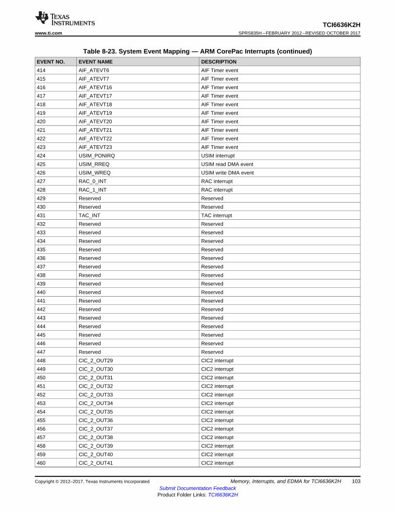
103
TCI6636K2Hwww.ti.com SPRS835H –FEBRUARY 2012–REVISED OCTOBER 2017
Submit Documentation FeedbackProduct Folder Links: TCI6636K2H
Memory, Interrupts, and EDMA for TCI6636K2HCopyright © 2012–2017, Texas Instruments Incorporated
Table 8-23. System Event Mapping — ARM CorePac Interrupts (continued)EVENT NO. EVENT NAME DESCRIPTION414 AIF_ATEVT6 AIF Timer event415 AIF_ATEVT7 AIF Timer event416 AIF_ATEVT16 AIF Timer event417 AIF_ATEVT17 AIF Timer event418 AIF_ATEVT18 AIF Timer event419 AIF_ATEVT19 AIF Timer event420 AIF_ATEVT20 AIF Timer event421 AIF_ATEVT21 AIF Timer event422 AIF_ATEVT22 AIF Timer event423 AIF_ATEVT23 AIF Timer event424 USIM_PONIRQ USIM interrupt425 USIM_RREQ USIM read DMA event426 USIM_WREQ USIM write DMA event427 RAC_0_INT RAC interrupt428 RAC_1_INT RAC interrupt429 Reserved Reserved430 Reserved Reserved431 TAC_INT TAC interrupt432 Reserved Reserved433 Reserved Reserved434 Reserved Reserved435 Reserved Reserved436 Reserved Reserved437 Reserved Reserved438 Reserved Reserved439 Reserved Reserved440 Reserved Reserved441 Reserved Reserved442 Reserved Reserved443 Reserved Reserved444 Reserved Reserved445 Reserved Reserved446 Reserved Reserved447 Reserved Reserved448 CIC_2_OUT29 CIC2 interrupt449 CIC_2_OUT30 CIC2 interrupt450 CIC_2_OUT31 CIC2 interrupt451 CIC_2_OUT32 CIC2 interrupt452 CIC_2_OUT33 CIC2 interrupt453 CIC_2_OUT34 CIC2 interrupt454 CIC_2_OUT35 CIC2 interrupt455 CIC_2_OUT36 CIC2 interrupt456 CIC_2_OUT37 CIC2 interrupt457 CIC_2_OUT38 CIC2 interrupt458 CIC_2_OUT39 CIC2 interrupt459 CIC_2_OUT40 CIC2 interrupt460 CIC_2_OUT41 CIC2 interrupt
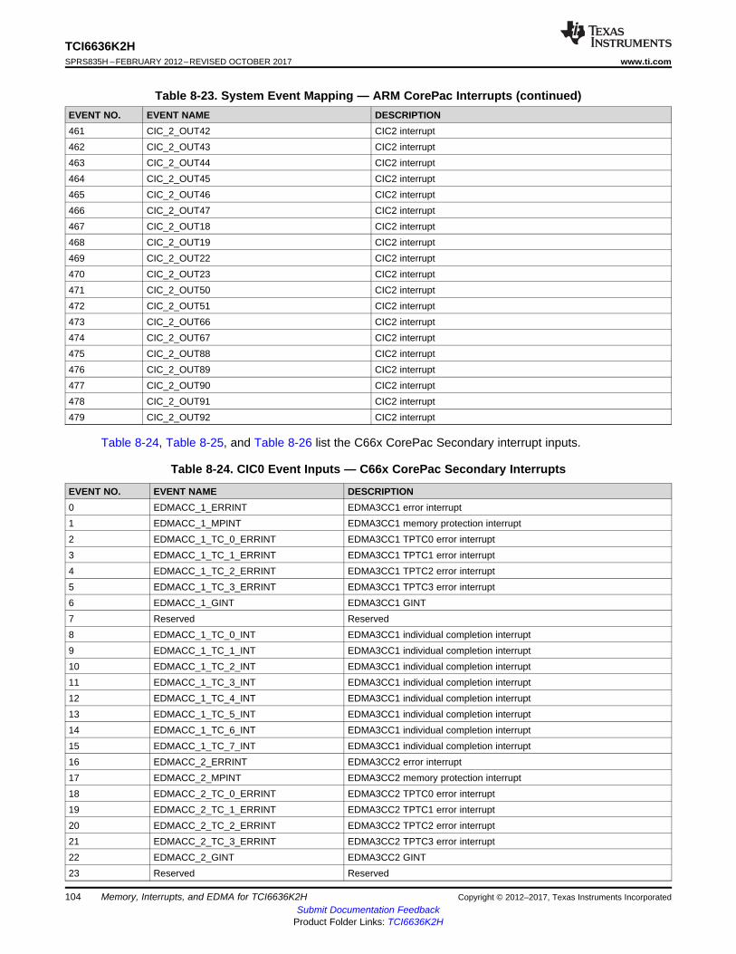
104
TCI6636K2HSPRS835H –FEBRUARY 2012–REVISED OCTOBER 2017 www.ti.com
Submit Documentation FeedbackProduct Folder Links: TCI6636K2H
Memory, Interrupts, and EDMA for TCI6636K2H Copyright © 2012–2017, Texas Instruments Incorporated
Table 8-23. System Event Mapping — ARM CorePac Interrupts (continued)EVENT NO. EVENT NAME DESCRIPTION461 CIC_2_OUT42 CIC2 interrupt462 CIC_2_OUT43 CIC2 interrupt463 CIC_2_OUT44 CIC2 interrupt464 CIC_2_OUT45 CIC2 interrupt465 CIC_2_OUT46 CIC2 interrupt466 CIC_2_OUT47 CIC2 interrupt467 CIC_2_OUT18 CIC2 interrupt468 CIC_2_OUT19 CIC2 interrupt469 CIC_2_OUT22 CIC2 interrupt470 CIC_2_OUT23 CIC2 interrupt471 CIC_2_OUT50 CIC2 interrupt472 CIC_2_OUT51 CIC2 interrupt473 CIC_2_OUT66 CIC2 interrupt474 CIC_2_OUT67 CIC2 interrupt475 CIC_2_OUT88 CIC2 interrupt476 CIC_2_OUT89 CIC2 interrupt477 CIC_2_OUT90 CIC2 interrupt478 CIC_2_OUT91 CIC2 interrupt479 CIC_2_OUT92 CIC2 interrupt
Table 8-24, Table 8-25, and Table 8-26 list the C66x CorePac Secondary interrupt inputs.
Table 8-24. CIC0 Event Inputs — C66x CorePac Secondary Interrupts
EVENT NO. EVENT NAME DESCRIPTION0 EDMACC_1_ERRINT EDMA3CC1 error interrupt1 EDMACC_1_MPINT EDMA3CC1 memory protection interrupt2 EDMACC_1_TC_0_ERRINT EDMA3CC1 TPTC0 error interrupt3 EDMACC_1_TC_1_ERRINT EDMA3CC1 TPTC1 error interrupt4 EDMACC_1_TC_2_ERRINT EDMA3CC1 TPTC2 error interrupt5 EDMACC_1_TC_3_ERRINT EDMA3CC1 TPTC3 error interrupt6 EDMACC_1_GINT EDMA3CC1 GINT7 Reserved Reserved8 EDMACC_1_TC_0_INT EDMA3CC1 individual completion interrupt9 EDMACC_1_TC_1_INT EDMA3CC1 individual completion interrupt10 EDMACC_1_TC_2_INT EDMA3CC1 individual completion interrupt11 EDMACC_1_TC_3_INT EDMA3CC1 individual completion interrupt12 EDMACC_1_TC_4_INT EDMA3CC1 individual completion interrupt13 EDMACC_1_TC_5_INT EDMA3CC1 individual completion interrupt14 EDMACC_1_TC_6_INT EDMA3CC1 individual completion interrupt15 EDMACC_1_TC_7_INT EDMA3CC1 individual completion interrupt16 EDMACC_2_ERRINT EDMA3CC2 error interrupt17 EDMACC_2_MPINT EDMA3CC2 memory protection interrupt18 EDMACC_2_TC_0_ERRINT EDMA3CC2 TPTC0 error interrupt19 EDMACC_2_TC_1_ERRINT EDMA3CC2 TPTC1 error interrupt20 EDMACC_2_TC_2_ERRINT EDMA3CC2 TPTC2 error interrupt21 EDMACC_2_TC_3_ERRINT EDMA3CC2 TPTC3 error interrupt22 EDMACC_2_GINT EDMA3CC2 GINT23 Reserved Reserved

105
TCI6636K2Hwww.ti.com SPRS835H –FEBRUARY 2012–REVISED OCTOBER 2017
Submit Documentation FeedbackProduct Folder Links: TCI6636K2H
Memory, Interrupts, and EDMA for TCI6636K2HCopyright © 2012–2017, Texas Instruments Incorporated
Table 8-24. CIC0 Event Inputs — C66x CorePac Secondary Interrupts (continued)EVENT NO. EVENT NAME DESCRIPTION24 EDMACC_2_TC_0_INT EDMA3CC2 individual completion interrupt25 EDMACC_2_TC_1_INT EDMA3CC2 individual completion interrupt26 EDMACC_2_TC_2_INT EDMA3CC2 individual completion interrupt27 EDMACC_2_TC_3_INT EDMA3CC2 individual completion interrupt28 EDMACC_2_TC_4_INT EDMA3CC2 individual completion interrupt29 EDMACC_2_TC_5_INT EDMA3CC2 individual completion interrupt30 EDMACC_2_TC_6_INT EDMA3CC2 individual completion interrupt31 EDMACC_2_TC_7_INT EDMA3CC2 individual completion interrupt32 EDMACC_0_ERRINT EDMA3CC0 error interrupt33 EDMACC_0_MPINT EDMA3CC0 memory protection interrupt34 EDMACC_0_TC_0_ERRINT EDMA3CC0 TPTC0 error interrupt35 EDMACC_0_TC_1_ERRINT EDMA3CC0 TPTC1 error interrupt36 EDMACC_0_GINT EDMA3CC0 global completion interrupt37 Reserved Reserved38 EDMACC_0_TC_0_INT EDMA3CC0 individual completion interrupt39 EDMACC_0_TC_1_INT EDMA3CC0 individual completion interrupt40 EDMACC_0_TC_2_INT EDMA3CC0 individual completion interrupt41 EDMACC_0_TC_3_INT EDMA3CC0 individual completion interrupt42 EDMACC_0_TC_4_INT EDMA3CC0 individual completion interrupt43 EDMACC_0_TC_5_INT EDMA3CC0 individual completion interrupt44 EDMACC_0_TC_6_INT EDMA3CC0 individual completion interrupt45 EDMACC_0_TC_7_INT EDMA3CC0 individual completion interrupt46 Reserved Reserved47 QMSS_QUE_PEND_652 Navigator transmit queue pending event for indicated queue48 PCIE_INT12 PCIE protocol error interrupt49 PCIE_INT13 PCIE power management interrupt50 PCIE_INT0 PCIE legacy INTA interrupt51 PCIE_INT1 PCIE legacy INTB interrupt52 PCIE_INT2 PCIE legacy INTC interrupt53 PCIE_INT3 PCIE legacy INTD interrupt54 SPI_0_INT0 SPI0 interrupt055 SPI_0_INT1 SPI0 interrupt156 SPI_0_XEVT SPI0 transmit event57 SPI_0_REVT SPI0 receive event58 I2C_0_INT I2C0 interrupt59 I2C_0_REVT I2C0 receive event60 I2C_0_XEVT I2C0 transmit event61 Reserved Reserved62 Reserved Reserved63 DBGTBR_DMAINT Debug trace buffer (TBR) DMA event64 MPU_12_INT MPU12 addressing violation interrupt and protection violation interrupt65 DBGTBR_ACQCOMP Debug trace buffer (TBR) acquisition has been completed66 MPU_13_INT MPU13 addressing violation interrupt and protection violation interrupt67 MPU_14_INT MPU14 addressing violation interrupt and protection violation interrupt68 NETCP_MDIO_LINK_INT0 Packet Accelerator 0 subsystem MDIO interrupt69 NETCP_MDIO_LINK_INT1 Packet Accelerator 0 subsystem MDIO interrupt70 NETCP_MDIO_USER_INT0 Packet Accelerator 0 subsystem MDIO interrupt

106
TCI6636K2HSPRS835H –FEBRUARY 2012–REVISED OCTOBER 2017 www.ti.com
Submit Documentation FeedbackProduct Folder Links: TCI6636K2H
Memory, Interrupts, and EDMA for TCI6636K2H Copyright © 2012–2017, Texas Instruments Incorporated
Table 8-24. CIC0 Event Inputs — C66x CorePac Secondary Interrupts (continued)EVENT NO. EVENT NAME DESCRIPTION71 NETCP_MDIO_USER_INT1 Packet Accelerator 0 subsystem MDIO interrupt72 NETCP_MISC_INT Packet Accelerator 0 subsystem misc interrupt73 TRACER_CORE_0_INT Tracer sliding time window interrupt for DSP0 L274 TRACER_CORE_1_INT Tracer sliding time window interrupt for DSP1 L275 TRACER_CORE_2_INT Tracer sliding time window interrupt for DSP2 L276 TRACER_CORE_3_INT Tracer sliding time window interrupt for DSP3 L277 TRACER_DDR_INT Tracer sliding time window interrupt for MSMC-DDR3A78 TRACER_MSMC_0_INT Tracer sliding time window interrupt for MSMC SRAM bank079 TRACER_MSMC_1_INT Tracer sliding time window interrupt for MSMC SRAM bank180 TRACER_MSMC_2_INT Tracer sliding time window interrupt for MSMC SRAM bank281 TRACER_MSMC_3_INT Tracer sliding time window interrupt for MSMC SRAM bank382 TRACER_CFG_INT Tracer sliding time window interrupt for CFG0 TeraNet83 TRACER_QMSS_QM_CFG1_INT Tracer sliding time window interrupt for Navigator CFG1 slave port84 TRACER_QMSS_DMA_INT Tracer sliding time window interrupt for Navigator DMA internal bus slave
port85 TRACER_SEM_INT Tracer sliding time window interrupt for Semaphore86 PSC_ALLINT Power & Sleep Controller interrupt87 MSMC_SCRUB_CERROR Correctable (1-bit) soft error detected during scrub cycle88 BOOTCFG_INT Chip-level MMR Error Register89 SR_0_PO_VCON_SMPSERR_INT SmartReflex SMPS error interrupt90 MPU_0_INT MPU0 addressing violation interrupt and protection violation interrupt91 QMSS_QUE_PEND_653 Navigator transmit queue pending event for indicated queue92 MPU_1_INT MPU1 addressing violation interrupt and protection violation interrupt.93 QMSS_QUE_PEND_654 Navigator transmit queue pending event for indicated queue94 MPU_2_INT MPU2 addressing violation interrupt and protection violation interrupt.95 QMSS_QUE_PEND_655 Navigator transmit queue pending event for indicated queue96 MPU_3_INT MPU3 addressing violation interrupt and protection violation interrupt.97 QMSS_QUE_PEND_656 Navigator transmit queue pending event for indicated queue98 MSMC_DEDC_CERROR Correctable (1-bit) soft error detected on SRAM read99 MSMC_DEDC_NC_ERROR Noncorrectable (2-bit) soft error detected on SRAM read100 MSMC_SCRUB_NC_ERROR Noncorrectable (2-bit) soft error detected during scrub cycle101 MSMC_MPF_ERROR0 Memory protection fault indicators for system master PrivID = 0102 MSMC_MPF_ERROR8 Memory protection fault indicators for system master PrivID = 8103 MSMC_MPF_ERROR9 Memory protection fault indicators for system master PrivID = 9104 MSMC_MPF_ERROR10 Memory protection fault indicators for system master PrivID = 10105 MSMC_MPF_ERROR11 Memory protection fault indicators for system master PrivID = 11106 MSMC_MPF_ERROR12 Memory protection fault indicators for system master PrivID = 12107 MSMC_MPF_ERROR13 Memory protection fault indicators for system master PrivID = 13108 MSMC_MPF_ERROR14 Memory protection fault indicators for system master PrivID = 14109 MSMC_MPF_ERROR15 Memory protection fault indicators for system master PrivID = 15110 DDR3_0_ERR DDR3A_EMIF error interrupt111 HYPERLINK_0_INT HyperLink 0 interrupt112 SRIO_INTDST0 SRIO interrupt113 SRIO_INTDST1 SRIO interrupt114 SRIO_INTDST2 SRIO interrupt115 SRIO_INTDST3 SRIO interrupt116 SRIO_INTDST4 SRIO interrupt117 SRIO_INTDST5 SRIO interrupt

107
TCI6636K2Hwww.ti.com SPRS835H –FEBRUARY 2012–REVISED OCTOBER 2017
Submit Documentation FeedbackProduct Folder Links: TCI6636K2H
Memory, Interrupts, and EDMA for TCI6636K2HCopyright © 2012–2017, Texas Instruments Incorporated
Table 8-24. CIC0 Event Inputs — C66x CorePac Secondary Interrupts (continued)EVENT NO. EVENT NAME DESCRIPTION118 SRIO_INTDST6 SRIO interrupt119 SRIO_INTDST7 SRIO interrupt120 SRIO_INTDST8 SRIO interrupt121 SRIO_INTDST9 SRIO interrupt122 SRIO_INTDST10 SRIO interrupt123 SRIO_INTDST11 SRIO interrupt124 SRIO_INTDST12 SRIO interrupt125 SRIO_INTDST13 SRIO interrupt126 SRIO_INTDST14 SRIO interrupt127 SRIO_INTDST15 SRIO interrupt128 AEMIF_EASYNCERR Asynchronous EMIF16 error interrupt129 TRACER_CORE_4_INT Tracer sliding time window interrupt for DSP4 L2130 TRACER_CORE_5_INT Tracer sliding time window interrupt for DSP5 L2131 TRACER_CORE_6_INT Tracer sliding time window interrupt for DSP6 L2132 TRACER_CORE_7_INT Tracer sliding time window interrupt for DSP7 L2133 QMSS_INTD_1_PKTDMA_0 Navigator interrupt for Packet DMA starvation134 QMSS_INTD_1_PKTDMA_1 Navigator interrupt for Packet DMA starvation135 SRIO_INT_PKTDMA_0 IPC interrupt generation136 NETCP_PKTDMA_INT0 Packet Accelerator0 Packet DMA starvation interrupt137 SR_0_SMARTREFLEX_INTREQ0 SmartReflex controller interrupt138 SR_0_SMARTREFLEX_INTREQ1 SmartReflex controller interrupt139 SR_0_SMARTREFLEX_INTREQ2 SmartReflex controller interrupt140 SR_0_SMARTREFLEX_INTREQ3 SmartReflex controller interrupt141 SR_0_VPNOSMPSACK SmartReflex VPVOLTUPDATE has been asserted but SMPS has not
been responded to in a defined time interval142 SR_0_VPEQVALUE SmartReflex SRSINTERUPT is asserted, but the new voltage is not
different from the current SMPS voltage143 SR_0_VPMAXVDD SmartReflex. The new voltage required is equal to or greater than MaxVdd144 SR_0_VPMINVDD SmartReflex. The new voltage required is equal to or less than MinVdd145 SR_0_VPINIDLE SmartReflex indicating that the FSM of voltage processor is in idle146 SR_0_VPOPPCHANGEDONE SmartReflex indicating that the average frequency error is within the
desired limit147 Reserved Reserved148 UART_0_UARTINT UART0 interrupt149 UART_0_URXEVT UART0 receive event150 UART_0_UTXEVT UART0 transmit event151 QMSS_QUE_PEND_657 Navigator transmit queue pending event for indicated queue152 QMSS_QUE_PEND_658 Navigator transmit queue pending event for indicated queue153 QMSS_QUE_PEND_659 Navigator transmit queue pending event for indicated queue154 QMSS_QUE_PEND_660 Navigator transmit queue pending event for indicated queue155 QMSS_QUE_PEND_661 Navigator transmit queue pending event for indicated queue156 QMSS_QUE_PEND_662 Navigator transmit queue pending event for indicated queue157 QMSS_QUE_PEND_663 Navigator transmit queue pending event for indicated queue158 QMSS_QUE_PEND_664 Navigator transmit queue pending event for indicated queue159 QMSS_QUE_PEND_665 Navigator transmit queue pending event for indicated queue160 SR_0_VPSMPSACK SmartReflex VPVOLTUPDATE asserted and SMPS has acknowledged in
a defined time interval161 ARM_TBR_DMA ARM trace buffer (TBR) DMA event

108
TCI6636K2HSPRS835H –FEBRUARY 2012–REVISED OCTOBER 2017 www.ti.com
Submit Documentation FeedbackProduct Folder Links: TCI6636K2H
Memory, Interrupts, and EDMA for TCI6636K2H Copyright © 2012–2017, Texas Instruments Incorporated
Table 8-24. CIC0 Event Inputs — C66x CorePac Secondary Interrupts (continued)EVENT NO. EVENT NAME DESCRIPTION162 ARM_TBR_ACQ ARM trace buffer (TBR) acquisition has been completed163 ARM_NINTERRIRQ ARM internal memory ECC error interrupt request164 ARM_NAXIERRIRQ ARM bus error interrupt request165 SR_0_SR_TEMPSENSOR SmartReflex temperature threshold crossing interrupt166 SR_0_SR_TIMERINT SmartReflex internal timer expiration interrupt167 AIF_ATEVT8 AIF timer event168 AIF_ATEVT9 AIF timer event169 AIF_ATEVT10 AIF timer event170 AIF_ATEVT11 AIF timer event171 AIF_ATEVT12 AIF timer event172 AIF_ATEVT13 AIF timer event173 AIF_ATEVT14 AIF timer event174 AIF_ATEVT15 AIF timer event175 TIMER_7_INTL Timer interrupt low176 TIMER_7_INTH Timer interrupt high177 TIMER_6_INTL Timer interrupt low178 TIMER_6_INTH Timer interrupt high179 TIMER_5_INTL Timer interrupt low180 TIMER_5_INTH Timer interrupt high181 TIMER_4_INTL Timer interrupt low182 TIMER_4_INTH Timer interrupt high183 TIMER_3_INTL Timer interrupt low184 TIMER_3_INTH Timer interrupt high185 TIMER_2_INTL Timer interrupt low186 TIMER_2_INTH Timer interrupt high187 TIMER_1_INTL Timer interrupt low188 TIMER_1_INTH Timer interrupt high189 TIMER_0_INTL Timer interrupt low190 TIMER_0_INTH Timer interrupt high191 TCP3D_0_INT TCP3d interrupt192 TCP3D_1_INT TCP3d interrupt193 Reserved Reserved194 Reserved Reserved195 TCP3D_0_REVT0 TCP3d event196 TCP3D_0_REVT1 TCP3d event197 TCP3D_1_REVT0 TCP3d event198 TCP3D_1_REVT1 TCP3d event199 Reserved Reserved200 Reserved Reserved201 Reserved Reserved202 Reserved Reserved203 TAC_INT TAC interrupt204 TAC_DEVT0 TAC debug event205 TAC_DEVT1 TAC debug event206 AIF_INT AIF interrupt207 EDMACC_4_ERRINT EDMA3CC4 error interrupt208 EDMACC_4_MPINT EDMA3CC4 memory protection interrupt

109
TCI6636K2Hwww.ti.com SPRS835H –FEBRUARY 2012–REVISED OCTOBER 2017
Submit Documentation FeedbackProduct Folder Links: TCI6636K2H
Memory, Interrupts, and EDMA for TCI6636K2HCopyright © 2012–2017, Texas Instruments Incorporated
Table 8-24. CIC0 Event Inputs — C66x CorePac Secondary Interrupts (continued)EVENT NO. EVENT NAME DESCRIPTION209 EDMACC_4_TC_0_ERRINT EDMA3CC4 TPTC0 error interrupt210 EDMACC_4_TC_1_ERRINT EDMA3CC4 TPTC1 error interrupt211 EDMACC_4_GINT EDMA3CC4 GINT212 EDMACC_4_TC_0_INT EDMA3CC4 individual completion interrupt213 EDMACC_4_TC_1_INT EDMA3CC4 individual completion interrupt214 EDMACC_4_TC_2_INT EDMA3CC4 individual completion interrupt215 EDMACC_4_TC_3_INT EDMA3CC4 individual completion interrupt216 EDMACC_4_TC_4_INT EDMA3CC4 individual completion interrupt217 EDMACC_4_TC_5_INT EDMA3CC4 individual completion interrupt218 EDMACC_4_TC_6_INT EDMA3CC4 individual completion interrupt219 EDMACC_4_TC_7_INT EDMA3CC4 individual completion interrupt220 EDMACC_3_ERRINT EDMA3CC3 error interrupt221 EDMACC_3_MPINT EDMA3CC3 memory protection interrupt222 EDMACC_3_TC_0_ERRINT EDMA3CC3 TPTC0 error interrupt223 EDMACC_3_TC_1_ERRINT EDMA3CC3 TPTC1 error interrupt224 EDMACC_3_GINT EDMA3CC3 GINT225 EDMACC_3_TC_0_INT EDMA3CC3 individual completion interrupt226 EDMACC_3_TC_1_INT EDMA3CC3 individual completion interrupt227 EDMACC_3_TC_2_INT EDMA3CC3 individual completion interrupt228 EDMACC_3_TC_3_INT EDMA3CC3 individual completion interrupt229 EDMACC_3_TC_4_INT EDMA3CC3 individual completion interrupt230 EDMACC_3_TC_5_INT EDMA3CC3 individual completion interrupt231 EDMACC_3_TC_6_INT EDMA3CC3 individual completion interrupt232 EDMACC_3_TC_7_INT EDMA3CC3 individual completion interrupt233 UART_1_UARTINT UART1 interrupt234 UART_1_URXEVT UART1 receive event235 UART_1_UTXEVT UART1 transmit event236 I2C_1_INT I2C1 interrupt237 I2C_1_REVT I2C1 receive event238 I2C_1_XEVT I2C1 transmit event239 SPI_1_INT0 SPI1 interrupt0240 SPI_1_INT1 SPI1 interrupt1241 SPI_1_XEVT SPI1 transmit event242 SPI_1_REVT SPI1 receive event243 MPU_5_INT MPU5 addressing violation interrupt and protection violation interrupt244 MPU_8_INT MPU8 addressing violation interrupt and protection violation interrupt245 MPU_9_INT MPU9 addressing violation interrupt and protection violation interrupt246 MPU_11_INT MPU11 addressing violation interrupt and protection violation interrupt247 MPU_4_INT MPU4 addressing violation interrupt and protection violation interrupt248 MPU_6_INT MPU6 addressing violation interrupt and protection violation interrupt249 MPU_7_INT MPU7 addressing violation interrupt and protection violation interrupt250 MPU_10_INT MPU10 addressing violation interrupt and protection violation interrupt251 SPI_2_INT0 SPI2 interrupt0252 SPI_2_INT1 SPI2 interrupt1253 SPI_2_XEVT SPI2 transmit event254 SPI_2_REVT SPI2 receive event255 I2C_2_INT I2C2 interrupt

110
TCI6636K2HSPRS835H –FEBRUARY 2012–REVISED OCTOBER 2017 www.ti.com
Submit Documentation FeedbackProduct Folder Links: TCI6636K2H
Memory, Interrupts, and EDMA for TCI6636K2H Copyright © 2012–2017, Texas Instruments Incorporated
Table 8-24. CIC0 Event Inputs — C66x CorePac Secondary Interrupts (continued)EVENT NO. EVENT NAME DESCRIPTION256 I2C_2_REVT I2C2 receive event257 I2C_2_XEVT I2C2 transmit event258 Reserved Reserved259 Reserved Reserved260 Reserved Reserved261 Reserved Reserved262 Reserved Reserved263 Reserved Reserved264 USIM_PONIRQ USIM interrupt265 USIM_RREQ USIM read DMA event266 USIM_WREQ USIM write DMA event267 BCP_INT0 BCP interrupt268 BCP_INT1 BCP interrupt269 BCP_INT2 BCP interrupt270 BCP_INT3 BCP interrupt271 RAC_0_TRACE_GCCP0 RAC trace272 RAC_0_TRACE_GCCP1 RAC trace273 RAC_1_TRACE_GCCP0 RAC trace274 RAC_1_TRACE_GCCP1 RAC trace275 Reserved Reserved276 Reserved Reserved277 Reserved Reserved278 Reserved Reserved279 TAC_DEVT2 TAC debug280 TAC_DEVT3 TAC debug281 TAC_DEVT4 TAC debug282 TAC_DEVT5 TAC debug283 Reserved Reserved284 Reserved Reserved285 Reserved Reserved286 Reserved Reserved287 Reserved Reserved288 Reserved Reserved289 Reserved Reserved290 TRACER_RAC_1_INT Tracer RAC interrupt291 TRACER_RAC_FE_INT Tracer RAC interrupt292 QMSS_QUE_PEND_666 Navigator transmit queue pending event for indicated queue293 QMSS_QUE_PEND_667 Navigator transmit queue pending event for indicated queue294 QMSS_QUE_PEND_668 Navigator transmit queue pending event for indicated queue295 QMSS_QUE_PEND_669 Navigator transmit queue pending event for indicated queue296 QMSS_QUE_PEND_670 Navigator transmit queue pending event for indicated queue297 QMSS_QUE_PEND_671 Navigator transmit queue pending event for indicated queue298 QMSS_QUE_PEND_8844 Navigator transmit queue pending event for indicated queue299 QMSS_QUE_PEND_8845 Navigator transmit queue pending event for indicated queue300 QMSS_QUE_PEND_8846 Navigator transmit queue pending event for indicated queue301 QMSS_QUE_PEND_8847 Navigator transmit queue pending event for indicated queue302 QMSS_QUE_PEND_8848 Navigator transmit queue pending event for indicated queue

111
TCI6636K2Hwww.ti.com SPRS835H –FEBRUARY 2012–REVISED OCTOBER 2017
Submit Documentation FeedbackProduct Folder Links: TCI6636K2H
Memory, Interrupts, and EDMA for TCI6636K2HCopyright © 2012–2017, Texas Instruments Incorporated
Table 8-24. CIC0 Event Inputs — C66x CorePac Secondary Interrupts (continued)EVENT NO. EVENT NAME DESCRIPTION303 QMSS_QUE_PEND_8849 Navigator transmit queue pending event for indicated queue304 QMSS_QUE_PEND_8850 Navigator transmit queue pending event for indicated queue305 QMSS_QUE_PEND_8851 Navigator transmit queue pending event for indicated queue306 QMSS_QUE_PEND_8852 Navigator transmit queue pending event for indicated queue307 QMSS_QUE_PEND_8853 Navigator transmit queue pending event for indicated queue308 QMSS_QUE_PEND_8854 Navigator transmit queue pending event for indicated queue309 QMSS_QUE_PEND_8855 Navigator transmit queue pending event for indicated queue310 QMSS_QUE_PEND_8856 Navigator transmit queue pending event for indicated queue311 QMSS_QUE_PEND_8857 Navigator transmit queue pending event for indicated queue312 QMSS_QUE_PEND_8858 Navigator transmit queue pending event for indicated queue313 QMSS_QUE_PEND_8859 Navigator transmit queue pending event for indicated queue314 QMSS_QUE_PEND_8860 Navigator transmit queue pending event for indicated queue315 QMSS_QUE_PEND_8861 Navigator transmit queue pending event for indicated queue316 QMSS_QUE_PEND_8862 Navigator transmit queue pending event for indicated queue317 QMSS_QUE_PEND_8863 Navigator transmit queue pending event for indicated queue318 QMSS_INTD_2_PKTDMA_0 Navigator ECC error interrupt319 QMSS_INTD_2_PKTDMA_1 Navigator ECC error interrupt320 QMSS_INTD_1_LOW_0 Navigator interrupt low321 QMSS_INTD_1_LOW_1 Navigator interrupt low322 QMSS_INTD_1_LOW_2 Navigator interrupt low323 QMSS_INTD_1_LOW_3 Navigator interrupt low324 QMSS_INTD_1_LOW_4 Navigator interrupt low325 QMSS_INTD_1_LOW_5 Navigator interrupt low326 QMSS_INTD_1_LOW_6 Navigator interrupt low327 QMSS_INTD_1_LOW_7 Navigator interrupt low328 QMSS_INTD_1_LOW_8 Navigator interrupt low329 QMSS_INTD_1_LOW_9 Navigator interrupt low330 QMSS_INTD_1_LOW_10 Navigator interrupt low331 QMSS_INTD_1_LOW_11 Navigator interrupt low332 QMSS_INTD_1_LOW_12 Navigator interrupt low333 QMSS_INTD_1_LOW_13 Navigator interrupt low334 QMSS_INTD_1_LOW_14 Navigator interrupt low335 QMSS_INTD_1_LOW_15 Navigator interrupt low336 QMSS_INTD_2_LOW_0 Navigator second interrupt low337 QMSS_INTD_2_LOW_1 Navigator second interrupt low338 QMSS_INTD_2_LOW_2 Navigator second interrupt low339 QMSS_INTD_2_LOW_3 Navigator second interrupt low340 QMSS_INTD_2_LOW_4 Navigator second interrupt low341 QMSS_INTD_2_LOW_5 Navigator second interrupt low342 QMSS_INTD_2_LOW_6 Navigator second interrupt low343 QMSS_INTD_2_LOW_7 Navigator second interrupt low344 QMSS_INTD_2_LOW_8 Navigator second interrupt low345 QMSS_INTD_2_LOW_9 Navigator second interrupt low346 QMSS_INTD_2_LOW_10 Navigator second interrupt low347 QMSS_INTD_2_LOW_11 Navigator second interrupt low348 QMSS_INTD_2_LOW_12 Navigator second interrupt low349 QMSS_INTD_2_LOW_13 Navigator second interrupt low

112
TCI6636K2HSPRS835H –FEBRUARY 2012–REVISED OCTOBER 2017 www.ti.com
Submit Documentation FeedbackProduct Folder Links: TCI6636K2H
Memory, Interrupts, and EDMA for TCI6636K2H Copyright © 2012–2017, Texas Instruments Incorporated
Table 8-24. CIC0 Event Inputs — C66x CorePac Secondary Interrupts (continued)EVENT NO. EVENT NAME DESCRIPTION350 QMSS_INTD_2_LOW_14 Navigator second interrupt low351 QMSS_INTD_2_LOW_15 Navigator second interrupt low352 TRACER_EDMACC_0 Tracer sliding time window interrupt for EDMA3CC0353 TRACER_EDMACC_123_INT Tracer sliding time window interrupt for EDMA3CC1, EDMA3CC2 and
EDMA3CC3354 TRACER_CIC_INT Tracer sliding time window interrupt for interrupt controllers (CIC)355 TRACER_MSMC_4_INT Tracer sliding time window interrupt for MSMC SRAM bank4356 TRACER_MSMC_5_INT Tracer sliding time window interrupt for MSMC SRAM bank5357 TRACER_MSMC_6_INT Tracer sliding time window interrupt for MSMC SRAM bank6358 TRACER_MSMC_7_INT Tracer sliding time window interrupt for MSMC SRAM bank7359 TRACER_SPI_ROM_EMIF_INT Tracer sliding time window interrupt for SPI/ROM/EMIF16 modules360 TRACER_QMSS_QM_CFG2_INT Tracer sliding time window interrupt for QM2361 TRACER_TAC_BE_INT Tracer TAC interrupt362 Reserved Reserved363 TRACER_DDR_1_INT Tracer sliding time window interrupt for DDR3B364 TRACER_BCR_INT Tracer sliding time window interrupt for BCR365 HYPERLINK_1_INT HyperLink 1 interrupt366 VCP_0_INT0 VCP interrupt367 VCP_0_INT1 VCP interrupt368 VCP_0_INT2 VCP interrupt369 VCP_0_INT3 VCP interrupt370 VCP_1_INT0 VCP interrupt371 VCP_1_INT1 VCP interrupt372 VCP_1_INT2 VCP interrupt373 VCP_1_INT3 VCP interrupt374 VCP_0_REVT0 VCP event375 VCP_0_XEVT0 VCP event376 VCP_0_REVT1 VCP event377 VCP_0_XEVT1 VCP event378 VCP_0_REVT2 VCP event379 VCP_0_XEVT2 VCP event380 VCP_0_REVT3 VCP event381 VCP_0_XEVT3 VCP event382 VCP_1_REVT0 VCP event383 VCP_1_XEVT0 VCP event384 VCP_1_REVT1 VCP event385 VCP_1_XEVT1 VCP event386 VCP_1_REVT2 VCP event387 VCP_1_XEVT2 VCP event388 VCP_1_REVT3 VCP event389 VCP_1_XEVT3 VCP event390 FFTC_0_INT0 FFTC interrupt391 FFTC_0_INT1 FFTC interrupt392 FFTC_0_INT2 FFTC interrupt393 FFTC_0_INT3 FFTC interrupt394 FFTC_1_INT0 FFTC interrupt395 FFTC_1_INT1 FFTC interrupt396 FFTC_1_INT2 FFTC interrupt

113
TCI6636K2Hwww.ti.com SPRS835H –FEBRUARY 2012–REVISED OCTOBER 2017
Submit Documentation FeedbackProduct Folder Links: TCI6636K2H
Memory, Interrupts, and EDMA for TCI6636K2HCopyright © 2012–2017, Texas Instruments Incorporated
Table 8-24. CIC0 Event Inputs — C66x CorePac Secondary Interrupts (continued)EVENT NO. EVENT NAME DESCRIPTION397 FFTC_1_INT3 FFTC interrupt398 FFTC_2_INT0 FFTC interrupt399 FFTC_2_INT1 FFTC interrupt400 FFTC_2_INT2 FFTC interrupt401 FFTC_2_INT3 FFTC interrupt402 FFTC_3_INT0 FFTC interrupt403 FFTC_3_INT1 FFTC interrupt404 FFTC_3_INT2 FFTC interrupt405 FFTC_3_INT3 FFTC interrupt406 Reserved Reserved407 Reserved Reserved408 Reserved Reserved409 Reserved Reserved410 Reserved Reserved411 Reserved Reserved412 Reserved Reserved413 Reserved Reserved414 AIF_ATEVT16 AIF timer event415 AIF_ATEVT17 AIF timer event416 AIF_ATEVT18 AIF timer event417 AIF_ATEVT19 AIF timer event418 AIF_ATEVT20 AIF timer event419 AIF_ATEVT21 AIF timer event420 AIF_ATEVT22 AIF timer event421 AIF_ATEVT23 AIF timer event422 USB_INT00 USB interrupt423 USB_INT04 USB interrupt424 USB_INT05 USB interrupt425 USB_INT06 USB interrupt426 USB_INT07 USB interrupt427 USB_INT08 USB interrupt428 USB_INT09 USB interrupt429 USB_INT10 USB interrupt430 USB_INT11 USB interrupt431 USB_MISCINT USB miscellaneous interrupt432 USB_OABSINT USB OABS interrupt433 TIMER_12_INTL Timer interrupt low434 TIMER_12_INTH Timer interrupt high435 TIMER_13_INTL Timer interrupt low436 TIMER_13_INTH Timer interrupt high437 TIMER_14_INTL Timer interrupt low438 TIMER_14_INTH Timer interrupt high439 TIMER_15_INTL Timer interrupt low440 TIMER_15_INTH Timer interrupt high441 TIMER_16_INTL Timer interrupt low442 TIMER_17_INTL Timer interrupt high443 TIMER_18_INTL Timer interrupt low

114
TCI6636K2HSPRS835H –FEBRUARY 2012–REVISED OCTOBER 2017 www.ti.com
Submit Documentation FeedbackProduct Folder Links: TCI6636K2H
Memory, Interrupts, and EDMA for TCI6636K2H Copyright © 2012–2017, Texas Instruments Incorporated
Table 8-24. CIC0 Event Inputs — C66x CorePac Secondary Interrupts (continued)EVENT NO. EVENT NAME DESCRIPTION444 TIMER_19_INTL Timer interrupt high445 DDR3_1_ERR DDR3B_EMIF error interrupt446 GPIO_INT16 GPIO interrupt447 GPIO_INT17 GPIO interrupt448 GPIO_INT18 GPIO interrupt449 GPIO_INT19 GPIO interrupt450 GPIO_INT20 GPIO interrupt451 GPIO_INT21 GPIO interrupt452 GPIO_INT22 GPIO interrupt453 GPIO_INT23 GPIO interrupt454 GPIO_INT24 GPIO interrupt455 GPIO_INT25 GPIO interrupt456 GPIO_INT26 GPIO interrupt457 GPIO_INT27 GPIO interrupt458 GPIO_INT28 GPIO interrupt459 GPIO_INT29 GPIO interrupt460 GPIO_INT30 GPIO interrupt461 GPIO_INT31 GPIO interrupt462 SRIO_INTDST16 SRIOI interrupt463 SRIO_INTDST17 SRIOI interrupt464 SRIO_INTDST18 SRIOI interrupt465 SRIO_INTDST19 SRIOI interrupt466 PCIE_INT4 PCIE MSI interrupt467 PCIE_INT5 PCIE MSI interrupt468 PCIE_INT6 PCIE MSI interrupt469 PCIE_INT7 PCIE MSI interrupt470 SEM_INT12 Semaphore interrupt471 SEM_INT13 Semaphore interrupt472 SEM_ERR12 Semaphore error interrupt473 SEM_ERR13 Semaphore error interrupt
Table 8-25. CIC1 Event Inputs — C66x CorePac Secondary Interrupts
EVENT NO. EVENT NAME DESCRIPTION0 EDMACC_1_ERRINT EDMA3CC1 error interrupt1 EDMACC_1_MPINT EDMA3CC1 memory protection interrupt2 EDMACC_1_TC_0_ERRINT EDMA3CC1 TPTC0 error interrupt3 EDMACC_1_TC_1_ERRINT EDMA3CC1 TPTC1 error interrupt4 EDMACC_1_TC_2_ERRINT EDMA3CC1 TPTC2 error interrupt5 EDMACC_1_TC_3_ERRINT EDMA3CC1 TPTC3 error interrupt6 EDMACC_1_GINT EDMA3CC1 GINT7 Reserved Reserved8 EDMACC_1_TC_0_INT EDMA3CC1 individual completion interrupt9 EDMACC_1_TC_1_INT EDMA3CC1 individual completion interrupt10 EDMACC_1_TC_2_INT EDMA3CC1 individual completion interrupt11 EDMACC_1_TC_3_INT EDMA3CC1 individual completion interrupt12 EDMACC_1_TC_4_INT EDMA3CC1 individual completion interrupt13 EDMACC_1_TC_5_INT EDMA3CC1 individual completion interrupt

115
TCI6636K2Hwww.ti.com SPRS835H –FEBRUARY 2012–REVISED OCTOBER 2017
Submit Documentation FeedbackProduct Folder Links: TCI6636K2H
Memory, Interrupts, and EDMA for TCI6636K2HCopyright © 2012–2017, Texas Instruments Incorporated
Table 8-25. CIC1 Event Inputs — C66x CorePac Secondary Interrupts (continued)EVENT NO. EVENT NAME DESCRIPTION14 EDMACC_1_TC_6_INT EDMA3CC1 individual completion interrupt15 EDMACC_1_TC_7_INT EDMA3CC1 individual completion interrupt16 EDMACC_2_ERRINT EDMA3CC2 error interrupt17 EDMACC_2_MPINT EDMA3CC2 memory protection interrupt18 EDMACC_2_TC_0_ERRINT EDMA3CC2 TPTC0 error interrupt19 EDMACC_2_TC_1_ERRINT EDMA3CC2 TPTC1 error interrupt20 EDMACC_2_TC_2_ERRINT EDMA3CC2 TPTC2 error interrupt21 EDMACC_2_TC_3_ERRINT EDMA3CC2 TPTC3 error interrupt22 EDMACC_2_GINT EDMA3CC2 GINT23 Reserved Reserved24 EDMACC_2_TC_0_INT EDMA3CC2 individual completion interrupt25 EDMACC_2_TC_1_INT EDMA3CC2 individual completion interrupt26 EDMACC_2_TC_2_INT EDMA3CC2 individual completion interrupt27 EDMACC_2_TC_3_INT EDMA3CC2 individual completion interrupt28 EDMACC_2_TC_4_INT EDMA3CC2 individual completion interrupt29 EDMACC_2_TC_5_INT EDMA3CC2 individual completion interrupt30 EDMACC_2_TC_6_INT EDMA3CC2 individual completion interrupt31 EDMACC_2_TC_7_INT EDMA3CC2 individual completion interrupt32 EDMACC_0_ERRINT EDMA3CC0 error interrupt33 EDMACC_0_MPINT EDMA3CC0 memory protection interrupt34 EDMACC_0_TC_0_ERRINT EDMA3CC0 TPTC0 error interrupt35 EDMACC_0_TC_1_ERRINT EDMA3CC0 TPTC1 error interrupt36 EDMACC_0_GINT EDMA3CC0 GINT37 Reserved Reserved38 EDMACC_0_TC_0_INT EDMA3CC0 individual completion interrupt39 EDMACC_0_TC_1_INT EDMA3CC0 individual completion interrupt40 EDMACC_0_TC_2_INT EDMA3CC0 individual completion interrupt41 EDMACC_0_TC_3_INT EDMA3CC0 individual completion interrupt42 EDMACC_0_TC_4_INT EDMA3CC0 individual completion interrupt43 EDMACC_0_TC_5_INT EDMA3CC0 individual completion interrupt44 EDMACC_0_TC_6_INT EDMA3CC0 individual completion interrupt45 EDMACC_0_TC_7_INT EDMA3CC0 individual completion interrupt46 Reserved Reserved47 QMSS_QUE_PEND_658 Navigator transmit queue pending event for indicated queue48 PCIE_INT12 PCIE interrupt49 PCIE_INT13 PCIE interrupt50 PCIE_INT0 PCIE interrupt51 PCIE_INT1 PCIE interrupt52 PCIE_INT2 PCIE interrupt53 PCIE_INT3 PCIE interrupt54 SPI_0_INT0 SPI0 interrupt55 SPI_0_INT1 SPI0 interrupt56 SPI_0_XEVT SPI0 transmit event57 SPI_0_REVT SPI0 receive event58 I2C_0_INT I2C0 interrupt59 I2C_0_REVT I2C0 receive event60 I2C_0_XEVT I2C0 transmit event

116
TCI6636K2HSPRS835H –FEBRUARY 2012–REVISED OCTOBER 2017 www.ti.com
Submit Documentation FeedbackProduct Folder Links: TCI6636K2H
Memory, Interrupts, and EDMA for TCI6636K2H Copyright © 2012–2017, Texas Instruments Incorporated
Table 8-25. CIC1 Event Inputs — C66x CorePac Secondary Interrupts (continued)EVENT NO. EVENT NAME DESCRIPTION61 Reserved Reserved62 Reserved Reserved63 DBGTBR_DMAINT Debug trace buffer (TBR) DMA event64 MPU_12_INT MPU12 interrupt65 DBGTBR_ACQCOMP Debug trace buffer (TBR) acquisition has been completed66 MPU_13_INT MPU13 interrupt67 MPU_14_INT MPU14 interrupt68 NETCP_MDIO_LINK_INT0 Packet Accelerator 0 subsystem MDIO interrupt69 NETCP_MDIO_LINK_INT1 Packet Accelerator 0 subsystem MDIO interrupt70 NETCP_MDIO_USER_INT0 Packet Accelerator 0 subsystem MDIO interrupt71 NETCP_MDIO_USER_INT1 Packet Accelerator 0 subsystem MDIO interrupt72 NETCP_MISC_INT Packet Accelerator 0 subsystem misc interrupt73 TRACER_CORE_0_INT Tracer sliding time window interrupt for DSP0 L274 TRACER_CORE_1_INT Tracer sliding time window interrupt for DSP1 L275 TRACER_CORE_2_INT Tracer sliding time window interrupt for DSP2 L276 TRACER_CORE_3_INT Tracer sliding time window interrupt for DSP3 L277 TRACER_DDR_INT Tracer sliding time window interrupt for MSMC-DDR3A78 TRACER_MSMC_0_INT Tracer sliding time window interrupt for MSMC SRAM bank079 TRACER_MSMC_1_INT Tracer sliding time window interrupt for MSMC SRAM bank180 TRACER_MSMC_2_INT Tracer sliding time window interrupt for MSMC SRAM bank281 TRACER_MSMC_3_INT Tracer sliding time window interrupt for MSMC SRAM bank382 TRACER_CFG_INT Tracer sliding time window interrupt for CFG0 TeraNet83 TRACER_QMSS_QM_CFG1_INT Tracer sliding time window interrupt for Navigator CFG1 slave port84 TRACER_QMSS_DMA_INT Tracer sliding time window interrupt for Navigator DMA internal bus slave
port85 TRACER_SEM_INT Tracer sliding time window interrupt for Semaphore86 PSC_ALLINT Power & Sleep Controller interrupt87 MSMC_SCRUB_CERROR Correctable (1-bit) soft error detected during scrub cycle88 BOOTCFG_INT Chip-level MMR Error Register89 SR_0_PO_VCON_SMPSERR_INT SmartReflex SMPS error interrupt90 MPU_0_INT MPU0 addressing violation interrupt and protection violation interrupt.91 QMSS_QUE_PEND_659 Navigator transmit queue pending event for indicated queue92 MPU_1_INT MPU1 addressing violation interrupt and protection violation interrupt.93 QMSS_QUE_PEND_660 Navigator transmit queue pending event for indicated queue94 MPU_2_INT MPU2 addressing violation interrupt and protection violation interrupt.95 QMSS_QUE_PEND_661 Navigator transmit queue pending event for indicated queue96 MPU_3_INT MPU3 addressing violation interrupt and protection violation interrupt.97 QMSS_QUE_PEND_662 Navigator transmit queue pending event for indicated queue98 MSMC_DEDC_CERROR Correctable (1-bit) soft error detected on SRAM read99 MSMC_DEDC_NC_ERROR Noncorrectable (2-bit) soft error detected on SRAM read100 MSMC_SCRUB_NC_ERROR Noncorrectable (2-bit) soft error detected during scrub cycle101 Reserved Reserved102 MSMC_MPF_ERROR8 Memory protection fault indicators for system master PrivID = 8103 MSMC_MPF_ERROR9 Memory protection fault indicators for system master PrivID = 9104 MSMC_MPF_ERROR10 Memory protection fault indicators for system master PrivID = 10105 MSMC_MPF_ERROR11 Memory protection fault indicators for system master PrivID = 11106 MSMC_MPF_ERROR12 Memory protection fault indicators for system master PrivID = 12107 MSMC_MPF_ERROR13 Memory protection fault indicators for system master PrivID = 13

117
TCI6636K2Hwww.ti.com SPRS835H –FEBRUARY 2012–REVISED OCTOBER 2017
Submit Documentation FeedbackProduct Folder Links: TCI6636K2H
Memory, Interrupts, and EDMA for TCI6636K2HCopyright © 2012–2017, Texas Instruments Incorporated
Table 8-25. CIC1 Event Inputs — C66x CorePac Secondary Interrupts (continued)EVENT NO. EVENT NAME DESCRIPTION108 MSMC_MPF_ERROR14 Memory protection fault indicators for system master PrivID = 14109 MSMC_MPF_ERROR15 Memory protection fault indicators for system master PrivID = 15110 DDR3_0_ERR DDR3A_EMIF Error interrupt111 HYPERLINK_0_INT HyperLink 0 interrupt112 SRIO_INTDST0 SRIO interrupt113 SRIO_INTDST1 SRIO interrupt114 SRIO_INTDST2 SRIO interrupt115 SRIO_INTDST3 SRIO interrupt116 SRIO_INTDST4 SRIO interrupt117 SRIO_INTDST5 SRIO interrupt118 SRIO_INTDST6 SRIO interrupt119 SRIO_INTDST7 SRIO interrupt120 SRIO_INTDST8 SRIO interrupt121 SRIO_INTDST9 SRIO interrupt122 SRIO_INTDST10 SRIO interrupt123 SRIO_INTDST11 SRIO interrupt124 SRIO_INTDST12 SRIO interrupt125 SRIO_INTDST13 SRIO interrupt126 SRIO_INTDST14 SRIO interrupt127 SRIO_INTDST15 SRIO interrupt128 AEMIF_EASYNCERR Asynchronous EMIF16 error interrupt129 TRACER_CORE_4_INT Tracer sliding time window interrupt for DSP4 L2130 TRACER_CORE_5_INT Tracer sliding time window interrupt for DSP5 L2131 TRACER_CORE_6_INT Tracer sliding time window interrupt for DSP6 L2132 TRACER_CORE_7_INT Tracer sliding time window interrupt for DSP7 L2133 QMSS_INTD_1_PKTDMA_0 Navigator interrupt for Packet DMA starvation134 QMSS_INTD_1_PKTDMA_1 Navigator interrupt for Packet DMA starvation135 SRIO_INT_PKTDMA_0 IPC interrupt generation136 NETCP_PKTDMA_INT0 Packet Accelerator0 Packet DMA starvation interrupt137 SR_0_SMARTREFLEX_INTREQ0 SmartReflex controller interrupt138 SR_0_SMARTREFLEX_INTREQ1 SmartReflex controller interrupt139 SR_0_SMARTREFLEX_INTREQ2 SmartReflex controller interrupt140 SR_0_SMARTREFLEX_INTREQ3 SmartReflex controller interrupt141 SR_0_VPNOSMPSACK SmartReflex VPVOLTUPDATE has been asserted but SMPS has not
been responded to in a defined time interval142 SR_0_VPEQVALUE SmartReflex SRSINTERUPT is asserted, but the new voltage is not
different from the current SMPS voltage143 SR_0_VPMAXVDD SmartReflex. The new voltage required is equal to or greater than MaxVdd144 SR_0_VPMINVDD SmartReflex. The new voltage required is equal to or less than MinVdd145 SR_0_VPINIDLE SmartReflex indicating that the FSM of voltage processor is in idle146 SR_0_VPOPPCHANGEDONE SmartReflex indicating that the average frequency error is within the
desired limit147 Reserved Reserved148 UART_0_UARTINT UART0 interrupt149 UART_0_URXEVT UART0 receive event150 UART_0_UTXEVT UART0 transmit event151 QMSS_QUE_PEND_663 Navigator transmit queue pending event for indicated queue152 QMSS_QUE_PEND_664 Navigator transmit queue pending event for indicated queue

118
TCI6636K2HSPRS835H –FEBRUARY 2012–REVISED OCTOBER 2017 www.ti.com
Submit Documentation FeedbackProduct Folder Links: TCI6636K2H
Memory, Interrupts, and EDMA for TCI6636K2H Copyright © 2012–2017, Texas Instruments Incorporated
Table 8-25. CIC1 Event Inputs — C66x CorePac Secondary Interrupts (continued)EVENT NO. EVENT NAME DESCRIPTION153 QMSS_QUE_PEND_665 Navigator transmit queue pending event for indicated queue154 QMSS_QUE_PEND_666 Navigator transmit queue pending event for indicated queue155 QMSS_QUE_PEND_667 Navigator transmit queue pending event for indicated queue156 QMSS_QUE_PEND_668 Navigator transmit queue pending event for indicated queue157 QMSS_QUE_PEND_669 Navigator transmit queue pending event for indicated queue158 QMSS_QUE_PEND_670 Navigator transmit queue pending event for indicated queue159 QMSS_QUE_PEND_671 Navigator transmit queue pending event for indicated queue160 SR_0_VPSMPSACK SmartReflex VPVOLTUPDATE asserted and SMPS has acknowledged in
a defined time interval161 ARM_TBR_DMA ARM trace buffer (TBR) DMA event162 ARM_TBR_ACQ ARM trace buffer (TBR) Acquisition has been completed163 ARM_NINTERRIRQ ARM internal memory ECC error interrupt request164 ARM_NAXIERRIRQ ARM bus error interrupt request165 SR_0_SR_TEMPSENSOR SmartReflex temperature threshold crossing interrupt166 SR_0_SR_TIMERINT SmartReflex internal timer expiration interrupt167 AIF_ATEVT8 AIF timer event168 AIF_ATEVT9 AIF timer event169 AIF_ATEVT10 AIF timer event170 AIF_ATEVT11 AIF timer event171 AIF_ATEVT12 AIF timer event172 AIF_ATEVT13 AIF timer event173 AIF_ATEVT14 AIF timer event174 AIF_ATEVT15 AIF timer event175 TIMER_7_INTL Timer interrupt low176 TIMER_7_INTH Timer interrupt high177 TIMER_6_INTL Timer interrupt low178 TIMER_6_INTH Timer interrupt high179 TIMER_5_INTL Timer interrupt low180 TIMER_5_INTH Timer interrupt high181 TIMER_4_INTL Timer interrupt low182 TIMER_4_INTH Timer interrupt high183 TIMER_3_INTL Timer interrupt low184 TIMER_3_INTH Timer interrupt high185 TIMER_2_INTL Timer interrupt low186 TIMER_2_INTH Timer interrupt high187 TIMER_1_INTL Timer interrupt low188 TIMER_1_INTH Timer interrupt high189 TIMER_0_INTL Timer interrupt low190 TIMER_0_INTH Timer interrupt high191 TCP3D_0_INT TCP3d interrupt192 TCP3D_1_INT TCP3d interrupt193 Reserved Reserved194 Reserved Reserved195 TCP3D_0_REVT0 TCP3d event196 TCP3D_0_REVT1 TCP3d event197 TCP3D_1_REVT0 TCP3d event198 TCP3D_1_REVT1 TCP3d event199 Reserved Reserved

119
TCI6636K2Hwww.ti.com SPRS835H –FEBRUARY 2012–REVISED OCTOBER 2017
Submit Documentation FeedbackProduct Folder Links: TCI6636K2H
Memory, Interrupts, and EDMA for TCI6636K2HCopyright © 2012–2017, Texas Instruments Incorporated
Table 8-25. CIC1 Event Inputs — C66x CorePac Secondary Interrupts (continued)EVENT NO. EVENT NAME DESCRIPTION200 Reserved Reserved201 Reserved Reserved202 Reserved Reserved203 TAC_INT TAC interrupt204 TAC_DEVT0 TAC debug event205 TAC_DEVT1 TAC debug event206 AIF_INT AIF interrupt207 EDMACC_4_ERRINT EDMA3CC4 error interrupt208 EDMACC_4_MPINT EDMA3CC4 memory protection interrupt209 EDMACC_4_TC_0_ERRINT EDMA3CC4 TPTC0 error interrupt210 EDMACC_4_TC_1_ERRINT EDMA3CC4 TPTC1 error interrupt211 EDMACC_4_GINT EDMA3CC4 GINT212 EDMACC_4_TC_0_INT EDMA3CC4 individual completion interrupt213 EDMACC_4_TC_1_INT EDMA3CC4 individual completion interrupt214 EDMACC_4_TC_2_INT EDMA3CC4 individual completion interrupt215 EDMACC_4_TC_3_INT EDMA3CC4 individual completion interrupt216 EDMACC_4_TC_4_INT EDMA3CC4 individual completion interrupt217 EDMACC_4_TC_5_INT EDMA3CC4 individual completion interrupt218 EDMACC_4_TC_6_INT EDMA3CC4 individual completion interrupt219 EDMACC_4_TC_7_INT EDMA3CC4 individual completion interrupt220 EDMACC_3_ERRINT EDMA3CC3 error interrupt221 EDMACC_3_MPINT EDMA3CC3 memory protection interrupt222 EDMACC_3_TC_0_ERRINT EDMA3CC3 TPTC0 error interrupt223 EDMACC_3_TC_1_ERRINT EDMA3CC3 TPTC1 error interrupt224 EDMACC_3_GINT EDMA3CC3 GINT225 EDMACC_3_TC_0_INT EDMA3CC3 individual completion interrupt226 EDMACC_3_TC_1_INT EDMA3CC3 individual completion interrupt227 EDMACC_3_TC_2_INT EDMA3CC3 individual completion interrupt228 EDMACC_3_TC_3_INT EDMA3CC3 individual completion interrupt229 EDMACC_3_TC_4_INT EDMA3CC3 individual completion interrupt230 EDMACC_3_TC_5_INT EDMA3CC3 individual completion interrupt231 EDMACC_3_TC_6_INT EDMA3CC3 individual completion interrupt232 EDMACC_3_TC_7_INT EDMA3CC3 individual completion interrupt233 UART_1_UARTINT UART1 interrupt234 UART_1_URXEVT UART1 receive event235 UART_1_UTXEVT UART1 transmit event236 I2C_1_INT I2C1 interrupt237 I2C_1_REVT I2C1 receive event238 I2C_1_XEVT I2C1 transmit event239 SPI_1_INT0 SPI1 interrupt0240 SPI_1_INT1 SPI1 interrupt1241 SPI_1_XEVT SPI1 transmit event242 SPI_1_REVT SPI1 receive event243 MPU_5_INT MPU5 addressing violation interrupt and protection violation interrupt244 MPU_8_INT MPU8 addressing violation interrupt and protection violation interrupt245 MPU_9_INT MPU9 addressing violation interrupt and protection violation interrupt246 MPU_11_INT MPU11 addressing violation interrupt and protection violation interrupt

120
TCI6636K2HSPRS835H –FEBRUARY 2012–REVISED OCTOBER 2017 www.ti.com
Submit Documentation FeedbackProduct Folder Links: TCI6636K2H
Memory, Interrupts, and EDMA for TCI6636K2H Copyright © 2012–2017, Texas Instruments Incorporated
Table 8-25. CIC1 Event Inputs — C66x CorePac Secondary Interrupts (continued)EVENT NO. EVENT NAME DESCRIPTION247 MPU_4_INT MPU4 addressing violation interrupt and protection violation interrupt248 MPU_6_INT MPU6 addressing violation interrupt and protection violation interrupt249 MPU_7_INT MPU7 addressing violation interrupt and protection violation interrupt250 MPU_10_INT MPU10 addressing violation interrupt and protection violation interrupt251 SPI_2_INT0 SPI2 interrupt0252 SPI_2_INT1 SPI2 interrupt1253 SPI_2_XEVT SPI2 transmit event254 SPI_2_REVT SPI2 receive event255 I2C_2_INT I2C2 interrupt256 I2C_2_REVT I2C2 receive event257 I2C_2_XEVT I2C2 transmit event258 Reserved Reserved259 Reserved Reserved260 Reserved Reserved261 Reserved Reserved262 Reserved Reserved263 Reserved Reserved264 USIM_PONIRQ USIM interrupt265 USIM_RREQ USIM read DMA event266 USIM_WREQ USIM write DMA event267 BCP_INT0 BCP interrupt268 BCP_INT1 BCP interrupt269 BCP_INT2 BCP interrupt270 BCP_INT3 BCP interrupt271 RAC_0_TRACE_GCCP0 RAC trace272 RAC_0_TRACE_GCCP1 RAC trace273 RAC_1_TRACE_GCCP0 RAC trace274 RAC_1_TRACE_GCCP1 RAC trace275 Reserved Reserved276 Reserved Reserved277 Reserved Reserved278 Reserved Reserved279 TAC_DEVT2 TAC debug280 TAC_DEVT3 TAC debug281 TAC_DEVT4 TAC debug282 TAC_DEVT5 TAC debug283 Reserved Reserved284 Reserved Reserved285 Reserved Reserved286 Reserved Reserved287 Reserved Reserved288 Reserved Reserved289 Reserved Reserved290 TRACER_RAC_1_INT Tracer RAC interrupt291 TRACER_RAC_FE_INT Tracer RAC interrupt292 QMSS_QUE_PEND_652 Navigator transmit queue pending event for indicated queue293 QMSS_QUE_PEND_653 Navigator transmit queue pending event for indicated queue

121
TCI6636K2Hwww.ti.com SPRS835H –FEBRUARY 2012–REVISED OCTOBER 2017
Submit Documentation FeedbackProduct Folder Links: TCI6636K2H
Memory, Interrupts, and EDMA for TCI6636K2HCopyright © 2012–2017, Texas Instruments Incorporated
Table 8-25. CIC1 Event Inputs — C66x CorePac Secondary Interrupts (continued)EVENT NO. EVENT NAME DESCRIPTION294 QMSS_QUE_PEND_654 Navigator transmit queue pending event for indicated queue295 QMSS_QUE_PEND_655 Navigator transmit queue pending event for indicated queue296 QMSS_QUE_PEND_656 Navigator transmit queue pending event for indicated queue297 QMSS_QUE_PEND_657 Navigator transmit queue pending event for indicated queue298 QMSS_QUE_PEND_8844 Navigator transmit queue pending event for indicated queue299 QMSS_QUE_PEND_8845 Navigator transmit queue pending event for indicated queue300 QMSS_QUE_PEND_8846 Navigator transmit queue pending event for indicated queue301 QMSS_QUE_PEND_8847 Navigator transmit queue pending event for indicated queue302 QMSS_QUE_PEND_8848 Navigator transmit queue pending event for indicated queue303 QMSS_QUE_PEND_8849 Navigator transmit queue pending event for indicated queue304 QMSS_QUE_PEND_8850 Navigator transmit queue pending event for indicated queue305 QMSS_QUE_PEND_8851 Navigator transmit queue pending event for indicated queue306 QMSS_QUE_PEND_8852 Navigator transmit queue pending event for indicated queue307 QMSS_QUE_PEND_8853 Navigator transmit queue pending event for indicated queue308 QMSS_QUE_PEND_8854 Navigator transmit queue pending event for indicated queue309 QMSS_QUE_PEND_8855 Navigator transmit queue pending event for indicated queue310 QMSS_QUE_PEND_8856 Navigator transmit queue pending event for indicated queue311 QMSS_QUE_PEND_8857 Navigator transmit queue pending event for indicated queue312 QMSS_QUE_PEND_8858 Navigator transmit queue pending event for indicated queue313 QMSS_QUE_PEND_8859 Navigator transmit queue pending event for indicated queue314 QMSS_QUE_PEND_8860 Navigator transmit queue pending event for indicated queue315 QMSS_QUE_PEND_8861 Navigator transmit queue pending event for indicated queue316 QMSS_QUE_PEND_8862 Navigator transmit queue pending event for indicated queue317 QMSS_QUE_PEND_8863 Navigator transmit queue pending event for indicated queue318 QMSS_INTD_2_PKTDMA_0 Navigator ECC error interrupt319 QMSS_INTD_2_PKTDMA_1 Navigator ECC error interrupt320 QMSS_INTD_1_LOW_0 Navigator interrupt low321 QMSS_INTD_1_LOW_1 Navigator interrupt low322 QMSS_INTD_1_LOW_2 Navigator interrupt low323 QMSS_INTD_1_LOW_3 Navigator interrupt low324 QMSS_INTD_1_LOW_4 Navigator interrupt low325 QMSS_INTD_1_LOW_5 Navigator interrupt low326 QMSS_INTD_1_LOW_6 Navigator interrupt low327 QMSS_INTD_1_LOW_7 Navigator interrupt low328 QMSS_INTD_1_LOW_8 Navigator interrupt low329 QMSS_INTD_1_LOW_9 Navigator interrupt low330 QMSS_INTD_1_LOW_10 Navigator interrupt low331 QMSS_INTD_1_LOW_11 Navigator interrupt low332 QMSS_INTD_1_LOW_12 Navigator interrupt low333 QMSS_INTD_1_LOW_13 Navigator interrupt low334 QMSS_INTD_1_LOW_14 Navigator interrupt low335 QMSS_INTD_1_LOW_15 Navigator interrupt low336 QMSS_INTD_2_LOW_0 Navigator second interrupt low337 QMSS_INTD_2_LOW_1 Navigator second interrupt low338 QMSS_INTD_2_LOW_2 Navigator second interrupt low339 QMSS_INTD_2_LOW_3 Navigator second interrupt low340 QMSS_INTD_2_LOW_4 Navigator second interrupt low

122
TCI6636K2HSPRS835H –FEBRUARY 2012–REVISED OCTOBER 2017 www.ti.com
Submit Documentation FeedbackProduct Folder Links: TCI6636K2H
Memory, Interrupts, and EDMA for TCI6636K2H Copyright © 2012–2017, Texas Instruments Incorporated
Table 8-25. CIC1 Event Inputs — C66x CorePac Secondary Interrupts (continued)EVENT NO. EVENT NAME DESCRIPTION341 QMSS_INTD_2_LOW_5 Navigator second interrupt low342 QMSS_INTD_2_LOW_6 Navigator second interrupt low343 QMSS_INTD_2_LOW_7 Navigator second interrupt low344 QMSS_INTD_2_LOW_8 Navigator second interrupt low345 QMSS_INTD_2_LOW_9 Navigator second interrupt low346 QMSS_INTD_2_LOW_10 Navigator second interrupt low347 QMSS_INTD_2_LOW_11 Navigator second interrupt low348 QMSS_INTD_2_LOW_12 Navigator second interrupt low349 QMSS_INTD_2_LOW_13 Navigator second interrupt low350 QMSS_INTD_2_LOW_14 Navigator second interrupt low351 QMSS_INTD_2_LOW_15 Navigator second interrupt low352 TRACER_EDMACC_0 Tracer sliding time window interrupt for EDMA3CC0353 TRACER_EDMACC_123_INT Tracer sliding time window interrupt for EDMA3CC1, EDMA3CC2 and
EDMA3CC3354 TRACER_CIC_INT Tracer sliding time window interrupt for interrupt controllers (CIC)355 TRACER_MSMC_4_INT Tracer sliding time window interrupt for MSMC SRAM bank4356 TRACER_MSMC_5_INT Tracer sliding time window interrupt for MSMC SRAM bank5357 TRACER_MSMC_6_INT Tracer sliding time window interrupt for MSMC SRAM bank6358 TRACER_MSMC_7_INT Tracer sliding time window interrupt for MSMC SRAM bank7359 TRACER_SPI_ROM_EMIF_INT Tracer sliding time window interrupt for SPI/ROM/EMIF16 modules360 TRACER_QMSS_QM_CFG2_INT Tracer sliding time window interrupt for QM2361 TRACER_TAC_BE_INT Tracer TAC interrupt362 Reserved Reserved363 TRACER_DDR_1_INT Tracer sliding time window interrupt for DDR3B364 TRACER_BCR_INT Tracer sliding time window interrupt for BCR365 HYPERLINK_1_INT HyperLink 1 interrupt366 VCP_0_INT0 VCP interrupt367 VCP_0_INT1 VCP interrupt368 VCP_0_INT2 VCP interrupt369 VCP_0_INT3 VCP interrupt370 VCP_1_INT0 VCP interrupt371 VCP_1_INT1 VCP interrupt372 VCP_1_INT2 VCP interrupt373 VCP_1_INT3 VCP interrupt374 VCP_0_REVT0 VCP event375 VCP_0_XEVT0 VCP event376 VCP_0_REVT1 VCP event377 VCP_0_XEVT1 VCP event378 VCP_0_REVT2 VCP event379 VCP_0_XEVT2 VCP event380 VCP_0_REVT3 VCP event381 VCP_0_XEVT3 VCP event382 VCP_1_REVT0 VCP event383 VCP_1_XEVT0 VCP event384 VCP_1_REVT1 VCP event385 VCP_1_XEVT1 VCP event386 VCP_1_REVT2 VCP event387 VCP_1_XEVT2 VCP event
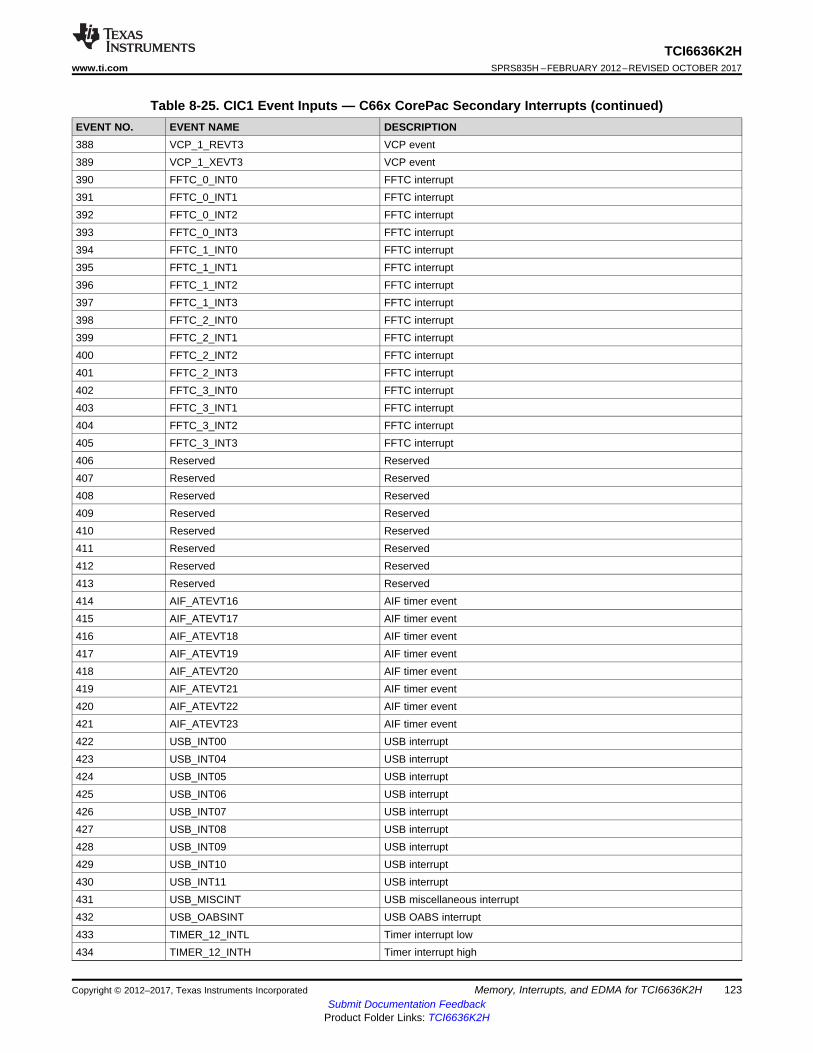
123
TCI6636K2Hwww.ti.com SPRS835H –FEBRUARY 2012–REVISED OCTOBER 2017
Submit Documentation FeedbackProduct Folder Links: TCI6636K2H
Memory, Interrupts, and EDMA for TCI6636K2HCopyright © 2012–2017, Texas Instruments Incorporated
Table 8-25. CIC1 Event Inputs — C66x CorePac Secondary Interrupts (continued)EVENT NO. EVENT NAME DESCRIPTION388 VCP_1_REVT3 VCP event389 VCP_1_XEVT3 VCP event390 FFTC_0_INT0 FFTC interrupt391 FFTC_0_INT1 FFTC interrupt392 FFTC_0_INT2 FFTC interrupt393 FFTC_0_INT3 FFTC interrupt394 FFTC_1_INT0 FFTC interrupt395 FFTC_1_INT1 FFTC interrupt396 FFTC_1_INT2 FFTC interrupt397 FFTC_1_INT3 FFTC interrupt398 FFTC_2_INT0 FFTC interrupt399 FFTC_2_INT1 FFTC interrupt400 FFTC_2_INT2 FFTC interrupt401 FFTC_2_INT3 FFTC interrupt402 FFTC_3_INT0 FFTC interrupt403 FFTC_3_INT1 FFTC interrupt404 FFTC_3_INT2 FFTC interrupt405 FFTC_3_INT3 FFTC interrupt406 Reserved Reserved407 Reserved Reserved408 Reserved Reserved409 Reserved Reserved410 Reserved Reserved411 Reserved Reserved412 Reserved Reserved413 Reserved Reserved414 AIF_ATEVT16 AIF timer event415 AIF_ATEVT17 AIF timer event416 AIF_ATEVT18 AIF timer event417 AIF_ATEVT19 AIF timer event418 AIF_ATEVT20 AIF timer event419 AIF_ATEVT21 AIF timer event420 AIF_ATEVT22 AIF timer event421 AIF_ATEVT23 AIF timer event422 USB_INT00 USB interrupt423 USB_INT04 USB interrupt424 USB_INT05 USB interrupt425 USB_INT06 USB interrupt426 USB_INT07 USB interrupt427 USB_INT08 USB interrupt428 USB_INT09 USB interrupt429 USB_INT10 USB interrupt430 USB_INT11 USB interrupt431 USB_MISCINT USB miscellaneous interrupt432 USB_OABSINT USB OABS interrupt433 TIMER_12_INTL Timer interrupt low434 TIMER_12_INTH Timer interrupt high

124
TCI6636K2HSPRS835H –FEBRUARY 2012–REVISED OCTOBER 2017 www.ti.com
Submit Documentation FeedbackProduct Folder Links: TCI6636K2H
Memory, Interrupts, and EDMA for TCI6636K2H Copyright © 2012–2017, Texas Instruments Incorporated
Table 8-25. CIC1 Event Inputs — C66x CorePac Secondary Interrupts (continued)EVENT NO. EVENT NAME DESCRIPTION435 TIMER_13_INTL Timer interrupt low436 TIMER_13_INTH Timer interrupt high437 TIMER_14_INTL Timer interrupt low438 TIMER_14_INTH Timer interrupt high439 TIMER_15_INTL Timer interrupt low440 TIMER_15_INTH Timer interrupt high441 TIMER_16_INTL Timer interrupt low442 TIMER_17_INTL Timer interrupt high443 TIMER_18_INTL Timer interrupt low444 TIMER_19_INTL Timer interrupt high445 DDR3_1_ERR DDR3B_EMIF error interrupt446 GPIO_INT16 GPIO interrupt447 GPIO_INT17 GPIO interrupt448 GPIO_INT18 GPIO interrupt449 GPIO_INT19 GPIO interrupt450 GPIO_INT20 GPIO interrupt451 GPIO_INT21 GPIO interrupt452 GPIO_INT22 GPIO interrupt453 GPIO_INT23 GPIO interrupt454 GPIO_INT24 GPIO interrupt455 GPIO_INT25 GPIO interrupt456 GPIO_INT26 GPIO interrupt457 GPIO_INT27 GPIO interrupt458 GPIO_INT28 GPIO interrupt459 GPIO_INT29 GPIO interrupt460 GPIO_INT30 GPIO interrupt461 GPIO_INT31 GPIO interrupt462 SRIO_INTDST20 SRIOI interrupt463 SRIO_INTDST21 SRIOI interrupt464 SRIO_INTDST22 SRIOI interrupt465 SRIO_INTDST23 SRIOI interrupt466 PCIE_INT8 PCIE MSI interrupt467 PCIE_INT9 PCIE MSI interrupt468 PCIE_INT10 PCIE MSI interrupt469 PCIE_INT11 PCIE MSI interrupt470 SEM_INT12 Semaphore interrupt471 SEM_INT13 Semaphore interrupt472 SEM_ERR12 Semaphore error interrupt473 SEM_ERR13 Semaphore error interrupt474 Reserved Reserved
Table 8-26. CIC2 Event Inputs (Secondary Events for EDMA3CC0 and Hyperlinks)
EVENT NO. EVENT NAME DESCRIPTION0 GPIO_INT8 GPIO interrupt1 GPIO_INT9 GPIO interrupt2 GPIO_INT10 GPIO interrupt3 GPIO_INT11 GPIO interrupt

125
TCI6636K2Hwww.ti.com SPRS835H –FEBRUARY 2012–REVISED OCTOBER 2017
Submit Documentation FeedbackProduct Folder Links: TCI6636K2H
Memory, Interrupts, and EDMA for TCI6636K2HCopyright © 2012–2017, Texas Instruments Incorporated
Table 8-26. CIC2 Event Inputs (Secondary Events for EDMA3CC0 and Hyperlinks) (continued)EVENT NO. EVENT NAME DESCRIPTION4 GPIO_INT12 GPIO interrupt5 GPIO_INT13 GPIO interrupt6 GPIO_INT14 GPIO interrupt7 GPIO_INT15 GPIO interrupt8 DBGTBR_DMAINT Debug trace buffer (TBR) DMA event9 Reserved Reserved10 Reserved Reserved11 TETB_FULLINT0 TETB0 is full12 TETB_HFULLINT0 TETB0 is half full13 TETB_ACQINT0 TETB0 acquisition has been completed14 TETB_FULLINT1 TETB1 is full15 TETB_HFULLINT1 TETB1 is half full16 TETB_ACQINT1 TETB1 acquisition has been completed17 TETB_FULLINT2 TETB2 is full18 TETB_HFULLINT2 TETB2 is half full19 TETB_ACQINT2 TETB2 acquisition has been completed20 TETB_FULLINT3 TETB3 is full21 TETB_HFULLINT3 TETB3 is half full22 TETB_ACQINT3 TETB3 acquisition has been completed23 Reserved Reserved24 QMSS_INTD_1_HIGH_16 Navigator hi interrupt25 QMSS_INTD_1_HIGH_17 Navigator hi interrupt26 QMSS_INTD_1_HIGH_18 Navigator hi interrupt27 QMSS_INTD_1_HIGH_19 Navigator hi interrupt28 QMSS_INTD_1_HIGH_20 Navigator hi interrupt29 QMSS_INTD_1_HIGH_21 Navigator hi interrupt30 QMSS_INTD_1_HIGH_22 Navigator hi interrupt31 QMSS_INTD_1_HIGH_23 Navigator hi interrupt32 QMSS_INTD_1_HIGH_24 Navigator hi interrupt33 QMSS_INTD_1_HIGH_25 Navigator hi interrupt34 QMSS_INTD_1_HIGH_26 Navigator hi interrupt35 QMSS_INTD_1_HIGH_27 Navigator hi interrupt36 QMSS_INTD_1_HIGH_28 Navigator hi interrupt37 QMSS_INTD_1_HIGH_29 Navigator hi interrupt38 QMSS_INTD_1_HIGH_30 Navigator hi interrupt39 QMSS_INTD_1_HIGH_31 Navigator hi interrupt40 NETCP_MDIO_LINK_INT0 Packet Accelerator 0 subsystem MDIO interrupt41 NETCP_MDIO_LINK_INT1 Packet Accelerator 0 subsystem MDIO interrupt42 NETCP_MDIO_USER_INT0 Packet Accelerator 0 subsystem MDIO interrupt43 NETCP_MDIO_USER_INT1 Packet Accelerator 0 subsystem MDIO interrupt44 NETCP_MISC_INT Packet Accelerator 0 subsystem MDIO interrupt45 TRACER_CORE_0_INT Tracer sliding time window interrupt for DSP0 L246 TRACER_CORE_1_INT Tracer sliding time window interrupt for DSP1 L247 TRACER_CORE_2_INT Tracer sliding time window interrupt for DSP2 L248 TRACER_CORE_3_INT Tracer sliding time window interrupt for DSP3 L249 TRACER_DDR_INT Tracer sliding time window interrupt for MSMC-DDR3A50 TRACER_MSMC_0_INT Tracer sliding time window interrupt for MSMC SRAM bank0

126
TCI6636K2HSPRS835H –FEBRUARY 2012–REVISED OCTOBER 2017 www.ti.com
Submit Documentation FeedbackProduct Folder Links: TCI6636K2H
Memory, Interrupts, and EDMA for TCI6636K2H Copyright © 2012–2017, Texas Instruments Incorporated
Table 8-26. CIC2 Event Inputs (Secondary Events for EDMA3CC0 and Hyperlinks) (continued)EVENT NO. EVENT NAME DESCRIPTION51 TRACER_MSMC_1_INT Tracer sliding time window interrupt for MSMC SRAM bank152 TRACER_MSMC_2_INT Tracer sliding time window interrupt for MSMC SRAM bank253 TRACER_MSMC_3_INT Tracer sliding time window interrupt for MSMC SRAM bank354 TRACER_CFG_INT Tracer sliding time window interrupt for TeraNet CFG55 TRACER_QMSS_QM_CFG1_INT Tracer sliding time window interrupt for Navigator CFG1 slave port56 TRACER_QMSS_DMA_INT Tracer sliding time window interrupt for Navigator DMA internal bus slave
port57 TRACER_SEM_INT Tracer sliding time window interrupt for Semaphore interrupt58 SEM_ERR0 Semaphore error interrupt59 SEM_ERR1 Semaphore error interrupt60 SEM_ERR2 Semaphore error interrupt61 SEM_ERR3 Semaphore error interrupt62 BOOTCFG_INT BOOTCFG error interrupt63 NETCP_PKTDMA_INT0 Packet Accelerator0 Packet DMA starvation interrupt64 MPU_0_INT MPU0 interrupt65 MSMC_SCRUB_CERROR MSMC error interrupt66 MPU_1_INT MPU1 interrupt67 SRIO_INT_PKTDMA_0 Packet Accelerator0 Packet DMA interrupt68 MPU_2_INT MPU2 interrupt69 QMSS_INTD_1_PKTDMA_0 Navigator Packet DMA interrupt70 MPU_3_INT MPU3 interrupt71 QMSS_INTD_1_PKTDMA_1 Navigator Packet DMA interrupt72 MSMC_DEDC_CERROR MSMC error interrupt73 MSMC_DEDC_NC_ERROR MSMC error interrupt74 MSMC_SCRUB_NC_ERROR MSMC error interrupt75 Reserved Reserved76 MSMC_MPF_ERROR0 Memory protection fault indicators for system master PrivID = 077 MSMC_MPF_ERROR1 Memory protection fault indicators for system master PrivID = 178 MSMC_MPF_ERROR2 Memory protection fault indicators for system master PrivID = 279 MSMC_MPF_ERROR3 Memory protection fault indicators for system master PrivID = 380 MSMC_MPF_ERROR4 Memory protection fault indicators for system master PrivID = 481 MSMC_MPF_ERROR5 Memory protection fault indicators for system master PrivID = 582 MSMC_MPF_ERROR6 Memory protection fault indicators for system master PrivID = 683 MSMC_MPF_ERROR7 Memory protection fault indicators for system master PrivID = 784 MSMC_MPF_ERROR8 Memory protection fault indicators for system master PrivID = 885 MSMC_MPF_ERROR9 Memory protection fault indicators for system master PrivID = 986 MSMC_MPF_ERROR10 Memory protection fault indicators for system master PrivID = 1087 MSMC_MPF_ERROR11 Memory protection fault indicators for system master PrivID = 1188 MSMC_MPF_ERROR12 Memory protection fault indicators for system master PrivID = 1289 MSMC_MPF_ERROR13 Memory protection fault indicators for system master PrivID = 1390 MSMC_MPF_ERROR14 Memory protection fault indicators for system master PrivID = 1491 MSMC_MPF_ERROR15 Memory protection fault indicators for system master PrivID = 1592 Reserved Reserved93 SRIO_INTDST0 SRIO interrupt94 SRIO_INTDST1 SRIO interrupt95 SRIO_INTDST2 SRIO interrupt96 SRIO_INTDST3 SRIO interrupt97 SRIO_INTDST4 SRIO interrupt

127
TCI6636K2Hwww.ti.com SPRS835H –FEBRUARY 2012–REVISED OCTOBER 2017
Submit Documentation FeedbackProduct Folder Links: TCI6636K2H
Memory, Interrupts, and EDMA for TCI6636K2HCopyright © 2012–2017, Texas Instruments Incorporated
Table 8-26. CIC2 Event Inputs (Secondary Events for EDMA3CC0 and Hyperlinks) (continued)EVENT NO. EVENT NAME DESCRIPTION98 SRIO_INTDST5 SRIO interrupt99 SRIO_INTDST6 SRIO interrupt100 SRIO_INTDST7 SRIO interrupt101 SRIO_INTDST8 SRIO interrupt102 SRIO_INTDST9 SRIO interrupt103 SRIO_INTDST10 SRIO interrupt104 SRIO_INTDST11 SRIO interrupt105 SRIO_INTDST12 SRIO interrupt106 SRIO_INTDST13 SRIO interrupt107 SRIO_INTDST14 SRIO interrupt108 SRIO_INTDST15 SRIO interrupt109 SRIO_INTDST16 SRIO interrupt110 SRIO_INTDST17 SRIO interrupt111 SRIO_INTDST18 SRIO interrupt112 SRIO_INTDST19 SRIO interrupt113 SRIO_INTDST20 SRIO interrupt114 SRIO_INTDST21 SRIO interrupt115 SRIO_INTDST22 SRIO interrupt116 SRIO_INTDST23 SRIO interrupt117 AEMIF_EASYNCERR Asynchronous EMIF16 error interrupt118 TETB_FULLINT4 TETB4 is full119 TETB_HFULLINT4 TETB4 is half full120 TETB_ACQINT4 TETB4 acquisition has been completed121 TETB_FULLINT5 TETB5 is full122 TETB_HFULLINT5 TETB5 is half full123 TETB_ACQINT5 TETB5 acquisition has been completed124 TETB_FULLINT6 TETB6 is full125 TETB_HFULLINT6 TETB6 is half full126 TETB_ACQINT6 TETB6 acquisition has been completed127 TETB_FULLINT7 TETB7 is full128 TETB_HFULLINT7 TETB7 is half full129 TETB_ACQINT7 TETB7 acquisition has been completed130 TRACER_CORE_4_INT Tracer sliding time window interrupt for DSP4 L2131 TRACER_CORE_5_INT Tracer sliding time window interrupt for DSP5 L2132 TRACER_CORE_6_INT Tracer sliding time window interrupt for DSP6 L2133 TRACER_CORE_7_INT Tracer sliding time window interrupt for DSP7 L2134 SEM_ERR4 Semaphore error interrupt135 SEM_ERR5 Semaphore error interrupt136 SEM_ERR6 Semaphore error interrupt137 SEM_ERR7 Semaphore error interrupt138 QMSS_INTD_1_HIGH_0 Navigator hi interrupt139 QMSS_INTD_1_HIGH_1 Navigator hi interrupt140 QMSS_INTD_1_HIGH_2 Navigator hi interrupt141 QMSS_INTD_1_HIGH_3 Navigator hi interrupt142 QMSS_INTD_1_HIGH_4 Navigator hi interrupt143 QMSS_INTD_1_HIGH_5 Navigator hi interrupt144 QMSS_INTD_1_HIGH_6 Navigator hi interrupt

128
TCI6636K2HSPRS835H –FEBRUARY 2012–REVISED OCTOBER 2017 www.ti.com
Submit Documentation FeedbackProduct Folder Links: TCI6636K2H
Memory, Interrupts, and EDMA for TCI6636K2H Copyright © 2012–2017, Texas Instruments Incorporated
Table 8-26. CIC2 Event Inputs (Secondary Events for EDMA3CC0 and Hyperlinks) (continued)EVENT NO. EVENT NAME DESCRIPTION145 QMSS_INTD_1_HIGH_7 Navigator hi interrupt146 QMSS_INTD_1_HIGH_8 Navigator hi interrupt147 QMSS_INTD_1_HIGH_9 Navigator hi interrupt148 QMSS_INTD_1_HIGH_10 Navigator hi interrupt149 QMSS_INTD_1_HIGH_11 Navigator hi interrupt150 QMSS_INTD_1_HIGH_12 Navigator hi interrupt151 QMSS_INTD_1_HIGH_13 Navigator hi interrupt152 QMSS_INTD_1_HIGH_14 Navigator hi interrupt153 QMSS_INTD_1_HIGH_15 Navigator hi interrupt154 QMSS_INTD_2_HIGH_0 Navigator second hi interrupt155 QMSS_INTD_2_HIGH_1 Navigator second hi interrupt156 QMSS_INTD_2_HIGH_2 Navigator second hi interrupt157 QMSS_INTD_2_HIGH_3 Navigator second hi interrupt158 QMSS_INTD_2_HIGH_4 Navigator second hi interrupt159 QMSS_INTD_2_HIGH_5 Navigator second hi interrupt160 QMSS_INTD_2_HIGH_6 Navigator second hi interrupt161 QMSS_INTD_2_HIGH_7 Navigator second hi interrupt162 QMSS_INTD_2_HIGH_8 Navigator second hi interrupt163 QMSS_INTD_2_HIGH_9 Navigator second hi interrupt164 QMSS_INTD_2_HIGH_10 Navigator second hi interrupt165 QMSS_INTD_2_HIGH_11 Navigator second hi interrupt166 QMSS_INTD_2_HIGH_12 Navigator second hi interrupt167 QMSS_INTD_2_HIGH_13 Navigator second hi interrupt168 QMSS_INTD_2_HIGH_14 Navigator second hi interrupt169 QMSS_INTD_2_HIGH_15 Navigator second hi interrupt170 QMSS_INTD_2_HIGH_16 Navigator second hi interrupt171 QMSS_INTD_2_HIGH_17 Navigator second hi interrupt172 QMSS_INTD_2_HIGH_18 Navigator second hi interrupt173 QMSS_INTD_2_HIGH_19 Navigator second hi interrupt174 QMSS_INTD_2_HIGH_20 Navigator second hi interrupt175 QMSS_INTD_2_HIGH_21 Navigator second hi interrupt176 QMSS_INTD_2_HIGH_22 Navigator second hi interrupt177 QMSS_INTD_2_HIGH_23 Navigator second hi interrupt178 QMSS_INTD_2_HIGH_24 Navigator second hi interrupt179 QMSS_INTD_2_HIGH_25 Navigator second hi interrupt180 QMSS_INTD_2_HIGH_26 Navigator second hi interrupt181 QMSS_INTD_2_HIGH_27 Navigator second hi interrupt182 QMSS_INTD_2_HIGH_28 Navigator second hi interrupt183 QMSS_INTD_2_HIGH_29 Navigator second hi interrupt184 QMSS_INTD_2_HIGH_30 Navigator second hi interrupt185 QMSS_INTD_2_HIGH_31 Navigator second hi interrupt186 MPU_12_INT MPU12 addressing violation interrupt and protection violation interrupt187 MPU_13_INT MPU13 addressing violation interrupt and protection violation interrupt188 MPU_14_INT MPU14 addressing violation interrupt and protection violation interrupt189 Reserved Reserved190 Reserved Reserved191 Reserved Reserved

129
TCI6636K2Hwww.ti.com SPRS835H –FEBRUARY 2012–REVISED OCTOBER 2017
Submit Documentation FeedbackProduct Folder Links: TCI6636K2H
Memory, Interrupts, and EDMA for TCI6636K2HCopyright © 2012–2017, Texas Instruments Incorporated
Table 8-26. CIC2 Event Inputs (Secondary Events for EDMA3CC0 and Hyperlinks) (continued)EVENT NO. EVENT NAME DESCRIPTION192 Reserved Reserved193 Reserved Reserved194 Reserved Reserved195 Reserved Reserved196 Reserved Reserved197 Reserved Reserved198 Reserved Reserved199 TRACER_QMSS_QM_CFG2_INT Tracer sliding time window interrupt for Navigator CFG2 slave port200 TRACER_EDMACC_0 Tracer sliding time window interrupt foR EDMA3CC0201 TRACER_EDMACC_123_INT Tracer sliding time window interrupt for EDMA3CC1, EDMA3CC2 and
EDMA3CC3202 TRACER_CIC_INT Tracer sliding time window interrupt for interrupt controllers (CIC)203 MPU_4_INT MPU4 addressing violation interrupt and protection violation interrupt204 MPU_5_INT MPU5 addressing violation interrupt and protection violation interrupt205 MPU_6_INT MPU6 addressing violation interrupt and protection violation interrupt206 MPU_7_INT MPU7 addressing violation interrupt and protection violation interrupt207 MPU_8_INT MPU8 addressing violation interrupt and protection violation interrupt208 QMSS_INTD_2_PKTDMA_0 Navigator ECC error interrupt209 QMSS_INTD_2_PKTDMA_1 Navigator ECC error interrupt210 SR_0_VPSMPSACK SmartReflex VPVOLTUPDATE asserted and SMPS has acknowledged in
a defined time interval211 DDR3_0_ERR DDR3A error interrupt212 HYPERLINK_0_INT HyperLink 0 interrupt213 EDMACC_0_ERRINT EDMA3CC0 error interrupt214 EDMACC_0_MPINT EDMA3CC0 memory protection interrupt215 EDMACC_0_TC_0_ERRINT EDMA3CC0 TPTC0 error interrupt216 EDMACC_0_TC_1_ERRINT EDMA3CC0 TPTC1 error interrupt217 EDMACC_1_ERRINT EDMA3CC1 error interrupt218 EDMACC_1_MPINT EDMA3CC1 memory protection interrupt219 EDMACC_1_TC_0_ERRINT EDMA3CC1 TPTC0 error interrupt220 EDMACC_1_TC_1_ERRINT EDMA3CC1 TPTC1 error interrupt221 EDMACC_1_TC_2_ERRINT EDMA3CC1 TPTC2 error interrupt222 EDMACC_1_TC_3_ERRINT EDMA3CC1 TPTC3 error interrupt223 EDMACC_2_ERRINT EDMA3CC2 error interrupt224 EDMACC_2_MPINT EDMA3CC2 memory protection interrupt225 EDMACC_2_TC_0_ERRINT EDMA3CC2 TPTC0 error interrupt226 EDMACC_2_TC_1_ERRINT EDMA3CC2 TPTC1 error interrupt227 EDMACC_2_TC_2_ERRINT EDMA3CC2 TPTC2 error interrupt228 EDMACC_2_TC_3_ERRINT EDMA3CC2 TPTC3 error interrupt229 EDMACC_3_ERRINT EDMA3CC3 error interrupt230 EDMACC_3_MPINT EDMA3CC3 memory protection interrupt231 EDMACC_3_TC_0_ERRINT EDMA3CC3 TPTC0 error interrupt232 EDMACC_3_TC_1_ERRINT EDMA3CC3 TPTC1 error interrupt233 EDMACC_4_ERRINT EDMA3CC4 error interrupt234 EDMACC_4_MPINT EDMA3CC4 memory protection interrupt235 EDMACC_4_TC_0_ERRINT EDMA3CC4 TPTC0 error interrupt236 EDMACC_4_TC_1_ERRINT EDMA3CC4 TPTC1 error interrupt237 QMSS_QUE_PEND_652 Navigator transmit queue pending event for indicated queue

130
TCI6636K2HSPRS835H –FEBRUARY 2012–REVISED OCTOBER 2017 www.ti.com
Submit Documentation FeedbackProduct Folder Links: TCI6636K2H
Memory, Interrupts, and EDMA for TCI6636K2H Copyright © 2012–2017, Texas Instruments Incorporated
Table 8-26. CIC2 Event Inputs (Secondary Events for EDMA3CC0 and Hyperlinks) (continued)EVENT NO. EVENT NAME DESCRIPTION238 QMSS_QUE_PEND_653 Navigator transmit queue pending event for indicated queue239 QMSS_QUE_PEND_654 Navigator transmit queue pending event for indicated queue240 QMSS_QUE_PEND_655 Navigator transmit queue pending event for indicated queue241 QMSS_QUE_PEND_656 Navigator transmit queue pending event for indicated queue242 QMSS_QUE_PEND_657 Navigator transmit queue pending event for indicated queue243 QMSS_QUE_PEND_658 Navigator transmit queue pending event for indicated queue244 QMSS_QUE_PEND_659 Navigator transmit queue pending event for indicated queue245 QMSS_QUE_PEND_660 Navigator transmit queue pending event for indicated queue246 QMSS_QUE_PEND_661 Navigator transmit queue pending event for indicated queue247 QMSS_QUE_PEND_662 Navigator transmit queue pending event for indicated queue248 QMSS_QUE_PEND_663 Navigator transmit queue pending event for indicated queue249 QMSS_QUE_PEND_664 Navigator transmit queue pending event for indicated queue250 QMSS_QUE_PEND_665 Navigator transmit queue pending event for indicated queue251 QMSS_QUE_PEND_666 Navigator transmit queue pending event for indicated queue252 QMSS_QUE_PEND_667 Navigator transmit queue pending event for indicated queue253 QMSS_QUE_PEND_668 Navigator transmit queue pending event for indicated queue254 QMSS_QUE_PEND_669 Navigator transmit queue pending event for indicated queue255 QMSS_QUE_PEND_670 Navigator transmit queue pending event for indicated queue256 QMSS_QUE_PEND_671 Navigator transmit queue pending event for indicated queue257 QMSS_QUE_PEND_8844 Navigator transmit queue pending event for indicated queue258 QMSS_QUE_PEND_8845 Navigator transmit queue pending event for indicated queue259 QMSS_QUE_PEND_8846 Navigator transmit queue pending event for indicated queue260 QMSS_QUE_PEND_8847 Navigator transmit queue pending event for indicated queue261 QMSS_QUE_PEND_8848 Navigator transmit queue pending event for indicated queue262 QMSS_QUE_PEND_8849 Navigator transmit queue pending event for indicated queue263 QMSS_QUE_PEND_8850 Navigator transmit queue pending event for indicated queue264 QMSS_QUE_PEND_8851 Navigator transmit queue pending event for indicated queue265 QMSS_QUE_PEND_8852 Navigator transmit queue pending event for indicated queue266 QMSS_QUE_PEND_8853 Navigator transmit queue pending event for indicated queue267 QMSS_QUE_PEND_8854 Navigator transmit queue pending event for indicated queue268 QMSS_QUE_PEND_8855 Navigator transmit queue pending event for indicated queue269 QMSS_QUE_PEND_8856 Navigator transmit queue pending event for indicated queue270 QMSS_QUE_PEND_8857 Navigator transmit queue pending event for indicated queue271 QMSS_QUE_PEND_8858 Navigator transmit queue pending event for indicated queue272 QMSS_QUE_PEND_8859 Navigator transmit queue pending event for indicated queue273 QMSS_QUE_PEND_8860 Navigator transmit queue pending event for indicated queue274 QMSS_QUE_PEND_8861 Navigator transmit queue pending event for indicated queue275 QMSS_QUE_PEND_8862 Navigator transmit queue pending event for indicated queue276 QMSS_QUE_PEND_8863 Navigator transmit queue pending event for indicated queue277 Reserved Reserved278 Reserved Reserved279 Reserved Reserved280 Reserved Reserved281 Reserved Reserved282 Reserved Reserved283 SEM_INT0 Semaphore interrupt284 SEM_INT1 Semaphore interrupt

131
TCI6636K2Hwww.ti.com SPRS835H –FEBRUARY 2012–REVISED OCTOBER 2017
Submit Documentation FeedbackProduct Folder Links: TCI6636K2H
Memory, Interrupts, and EDMA for TCI6636K2HCopyright © 2012–2017, Texas Instruments Incorporated
Table 8-26. CIC2 Event Inputs (Secondary Events for EDMA3CC0 and Hyperlinks) (continued)EVENT NO. EVENT NAME DESCRIPTION285 SEM_INT2 Semaphore interrupt286 SEM_INT3 Semaphore interrupt287 SEM_INT4 Semaphore interrupt288 SEM_INT5 Semaphore interrupt289 SEM_INT6 Semaphore interrupt290 SEM_INT7 Semaphore interrupt291 SEM_INT8 Semaphore interrupt292 SEM_INT9 Semaphore interrupt293 SEM_INT10 Semaphore interrupt294 SEM_INT11 Semaphore interrupt295 SEM_INT12 Semaphore interrupt296 SEM_INT13 Semaphore interrupt297 SEM_INT14 Semaphore interrupt298 SEM_INT15 Semaphore interrupt299 SEM_ERR8 Semaphore error interrupt300 SEM_ERR9 Semaphore error interrupt301 SEM_ERR10 Semaphore error interrupt302 SEM_ERR11 Semaphore error interrupt303 SEM_ERR12 Semaphore error interrupt304 SEM_ERR13 Semaphore error interrupt305 SEM_ERR14 Semaphore error interrupt306 SEM_ERR15 Semaphore error interrupt307 DDR3_1_ERR DDR3B error interrupt308 HYPERLINK_1_INT HyperLink 1 interrupt309 FFTC_0_INT0 FFTC interrupt310 FFTC_0_INT1 FFTC interrupt311 FFTC_0_INT2 FFTC interrupt312 FFTC_0_INT3 FFTC interrupt313 FFTC_1_INT0 FFTC interrupt314 FFTC_1_INT1 FFTC interrupt315 FFTC_1_INT2 FFTC interrupt316 FFTC_1_INT3 FFTC interrupt317 FFTC_2_INT0 FFTC interrupt318 FFTC_2_INT1 FFTC interrupt319 FFTC_2_INT2 FFTC interrupt320 FFTC_2_INT3 FFTC interrupt321 FFTC_3_INT0 FFTC interrupt322 FFTC_3_INT1 FFTC interrupt323 FFTC_3_INT2 FFTC interrupt324 FFTC_3_INT3 FFTC interrupt325 Reserved Reserved326 Reserved Reserved327 Reserved Reserved328 Reserved Reserved329 Reserved Reserved330 Reserved Reserved331 Reserved Reserved

132
TCI6636K2HSPRS835H –FEBRUARY 2012–REVISED OCTOBER 2017 www.ti.com
Submit Documentation FeedbackProduct Folder Links: TCI6636K2H
Memory, Interrupts, and EDMA for TCI6636K2H Copyright © 2012–2017, Texas Instruments Incorporated
Table 8-26. CIC2 Event Inputs (Secondary Events for EDMA3CC0 and Hyperlinks) (continued)EVENT NO. EVENT NAME DESCRIPTION332 Reserved Reserved333 AIF_INT AIF interrupt334 AIF_ATEVT0 AIF timer event335 AIF_ATEVT1 AIF timer event336 AIF_ATEVT2 AIF timer event337 AIF_ATEVT3 AIF timer event338 AIF_ATEVT4 AIF timer event339 AIF_ATEVT5 AIF timer event340 AIF_ATEVT6 AIF timer event341 AIF_ATEVT7 AIF timer event342 AIF_ATEVT8 AIF timer event343 AIF_ATEVT9 AIF timer event344 AIF_ATEVT10 AIF timer event345 AIF_ATEVT11 AIF timer event346 AIF_ATEVT12 AIF timer event347 AIF_ATEVT13 AIF timer event348 AIF_ATEVT14 AIF timer event349 AIF_ATEVT15 AIF timer event350 Reserved Reserved351 Reserved Reserved352 Reserved Reserved353 Reserved Reserved354 TCP3D_0_INT TCP3d interrupt355 TCP3D_1_INT TCP3d interrupt356 Reserved Reserved357 Reserved Reserved358 BCP_INT0 BCP interrupt359 BCP_INT1 BCP interrupt360 BCP_INT2 BCP interrupt361 BCP_INT3 BCP interrupt362 PSC_ALLINT PSC interrupt363 Reserved Reserved364 RAC_0_TRACE_GCCP0 RAC trace365 RAC_0_TRACE_GCCP1 RAC trace366 RAC_1_TRACE_GCCP0 RAC trace367 RAC_1_TRACE_GCCP1 RAC trace368 Reserved Reserved369 Reserved Reserved370 Reserved Reserved371 Reserved Reserved372 MPU_9_INT MPU9 addressing violation interrupt and protection violation interrupt373 MPU_10_INT MPU10 addressing violation interrupt and protection violation interrupt374 MPU_11_INT MPU11 addressing violation interrupt and protection violation interrupt375 TRACER_MSMC_4_INT Tracer sliding time window interrupt for MSMC SRAM Bank 4376 TRACER_MSMC_5_INT Tracer sliding time window interrupt for MSMC SRAM Bank 4377 TRACER_MSMC_6_INT Tracer sliding time window interrupt for MSMC SRAM Bank 4378 TRACER_MSMC_7_INT Tracer sliding time window interrupt for MSMC SRAM Bank 4

133
TCI6636K2Hwww.ti.com SPRS835H –FEBRUARY 2012–REVISED OCTOBER 2017
Submit Documentation FeedbackProduct Folder Links: TCI6636K2H
Memory, Interrupts, and EDMA for TCI6636K2HCopyright © 2012–2017, Texas Instruments Incorporated
Table 8-26. CIC2 Event Inputs (Secondary Events for EDMA3CC0 and Hyperlinks) (continued)EVENT NO. EVENT NAME DESCRIPTION379 TRACER_DDR_1_INT Tracer sliding time window interrupt for DDR3B380 TRACER_BCR_INT Tracer sliding time window interrupt for BCR381 TRACER_RAC_1_INT Tracer sliding time window interrupt for RAC382 Reserved Reserved383 TRACER_RAC_FE_INT Tracer sliding time window interrupt for RAC384 TRACER_SPI_ROM_EMIF_INT Tracer sliding time window interrupt for SPI/ROM/EMIF16 modules385 TRACER_TAC_BE_INT Tracer sliding time window interrupt for TAC386 Reserved Reserved387 TIMER_8_INTL Timer interrupt low388 TIMER_8_INTH Timer interrupt high389 TIMER_9_INTL Timer interrupt low390 TIMER_9_INTH Timer interrupt high391 TIMER_10_INTL Timer interrupt low392 TIMER_10_INTH Timer interrupt high393 TIMER_11_INTL Timer interrupt low394 TIMER_11_INTH Timer interrupt high395 TIMER_14_INTL Timer interrupt low396 TIMER_14_INTH Timer interrupt high397 TIMER_15_INTL Timer interrupt low398 TIMER_15_INTH Timer interrupt high399 USB_INT00 USB interrupt400 USB_INT04 USB interrupt401 USB_INT05 USB interrupt402 USB_INT06 USB interrupt403 USB_INT07 USB interrupt404 USB_INT08 USB interrupt405 USB_INT09 USB interrupt406 USB_INT10 USB interrupt407 USB_INT11 USB interrupt408 USB_MISCINT USB miscellaneous interrupt409 USB_OABSINT USB OABS interrupt410 TCP3D_0_REVT0 TCP3d interrupt411 TCP3D_0_REVT1 TCP3d interrupt412 TCP3D_1_REVT0 TCP3d interrupt413 TCP3D_1_REVT1 TCP3d interrupt414 Reserved Reserved415 Reserved Reserved416 Reserved Reserved417 Reserved Reserved418 VCP_0_INT0 VCP interrupt419 VCP_0_INT1 VCP interrupt420 VCP_0_INT2 VCP interrupt421 VCP_0_INT3 VCP interrupt422 VCP_1_INT0 VCP interrupt423 VCP_1_INT1 VCP interrupt424 VCP_1_INT2 VCP interrupt425 VCP_1_INT3 VCP interrupt

134
TCI6636K2HSPRS835H –FEBRUARY 2012–REVISED OCTOBER 2017 www.ti.com
Submit Documentation FeedbackProduct Folder Links: TCI6636K2H
Memory, Interrupts, and EDMA for TCI6636K2H Copyright © 2012–2017, Texas Instruments Incorporated
Table 8-26. CIC2 Event Inputs (Secondary Events for EDMA3CC0 and Hyperlinks) (continued)EVENT NO. EVENT NAME DESCRIPTION426 VCP_0_REVT0 VCP interrupt427 VCP_0_XEVT0 VCP interrupt428 VCP_0_REVT1 VCP interrupt429 VCP_0_XEVT1 VCP interrupt430 VCP_0_REVT2 VCP interrupt431 VCP_0_XEVT2 VCP interrupt432 VCP_0_REVT3 VCP interrupt433 VCP_0_XEVT3 VCP interrupt434 VCP_1_REVT0 VCP interrupt435 VCP_1_XEVT0 VCP interrupt436 VCP_1_REVT1 VCP interrupt437 VCP_1_XEVT1 VCP interrupt438 VCP_1_REVT2 VCP interrupt439 VCP_1_XEVT2 VCP interrupt440 VCP_1_REVT3 VCP interrupt441 VCP_1_XEVT3 VCP interrupt442 TETB_OVFLINT0 ETB0 overflow (emulation trace buffer)443 TETB_UNFLINT0 ETB0 underflow444 TETB_OVFLINT1 ETB1 overflow (emulation trace buffer)445 TETB_UNFLINT1 ETB1 underflow446 TETB_OVFLINT2 ETB2 overflow (emulation trace buffer)447 TETB_UNFLINT2 ETB2 underflow448 TETB_OVFLINT3 ETB3 overflow (emulation trace buffer)449 TETB_UNFLINT3 ETB3 underflow450 TETB_OVFLINT4 ETB4 overflow (emulation trace buffer)451 TETB_UNFLINT4 ETB4 underflow452 TETB_OVFLINT5 ETB5 overflow (emulation trace buffer)453 TETB_UNFLINT5 ETB5 underflow454 TETB_OVFLINT6 ETB6 overflow (emulation trace buffer)455 TETB_UNFLINT6 ETB6 underflow456 TETB_OVFLINT7 ETB7 overflow (emulation trace buffer)457 TETB_UNFLINT7 ETB7 underflow458 ARM_TBR_DMA ARM trace buffer459 RAC_0_INT RAC interrupt460 RAC_1_INT RAC interrupt461 Reserved Reserved462 Reserved Reserved463 GPIO_INT0 GPIO interrupt464 GPIO_INT1 GPIO interrupt465 GPIO_INT2 GPIO interrupt466 GPIO_INT3 GPIO interrupt467 GPIO_INT4 GPIO interrupt468 GPIO_INT5 GPIO interrupt469 GPIO_INT6 GPIO interrupt470 GPIO_INT7 GPIO interrupt471 IPC_GR0 IPC interrupt generation472 IPC_GR1 IPC interrupt generation
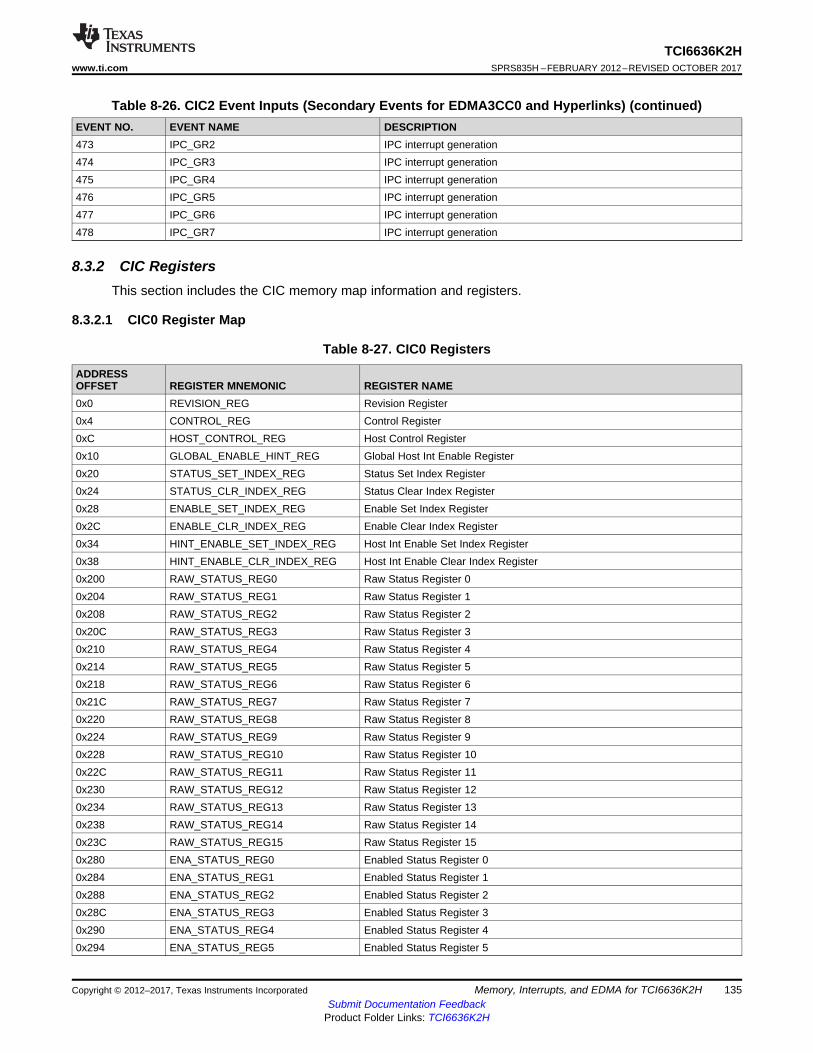
135
TCI6636K2Hwww.ti.com SPRS835H –FEBRUARY 2012–REVISED OCTOBER 2017
Submit Documentation FeedbackProduct Folder Links: TCI6636K2H
Memory, Interrupts, and EDMA for TCI6636K2HCopyright © 2012–2017, Texas Instruments Incorporated
Table 8-26. CIC2 Event Inputs (Secondary Events for EDMA3CC0 and Hyperlinks) (continued)EVENT NO. EVENT NAME DESCRIPTION473 IPC_GR2 IPC interrupt generation474 IPC_GR3 IPC interrupt generation475 IPC_GR4 IPC interrupt generation476 IPC_GR5 IPC interrupt generation477 IPC_GR6 IPC interrupt generation478 IPC_GR7 IPC interrupt generation
8.3.2 CIC RegistersThis section includes the CIC memory map information and registers.
8.3.2.1 CIC0 Register Map
Table 8-27. CIC0 Registers
ADDRESSOFFSET REGISTER MNEMONIC REGISTER NAME0x0 REVISION_REG Revision Register0x4 CONTROL_REG Control Register0xC HOST_CONTROL_REG Host Control Register0x10 GLOBAL_ENABLE_HINT_REG Global Host Int Enable Register0x20 STATUS_SET_INDEX_REG Status Set Index Register0x24 STATUS_CLR_INDEX_REG Status Clear Index Register0x28 ENABLE_SET_INDEX_REG Enable Set Index Register0x2C ENABLE_CLR_INDEX_REG Enable Clear Index Register0x34 HINT_ENABLE_SET_INDEX_REG Host Int Enable Set Index Register0x38 HINT_ENABLE_CLR_INDEX_REG Host Int Enable Clear Index Register0x200 RAW_STATUS_REG0 Raw Status Register 00x204 RAW_STATUS_REG1 Raw Status Register 10x208 RAW_STATUS_REG2 Raw Status Register 20x20C RAW_STATUS_REG3 Raw Status Register 30x210 RAW_STATUS_REG4 Raw Status Register 40x214 RAW_STATUS_REG5 Raw Status Register 50x218 RAW_STATUS_REG6 Raw Status Register 60x21C RAW_STATUS_REG7 Raw Status Register 70x220 RAW_STATUS_REG8 Raw Status Register 80x224 RAW_STATUS_REG9 Raw Status Register 90x228 RAW_STATUS_REG10 Raw Status Register 100x22C RAW_STATUS_REG11 Raw Status Register 110x230 RAW_STATUS_REG12 Raw Status Register 120x234 RAW_STATUS_REG13 Raw Status Register 130x238 RAW_STATUS_REG14 Raw Status Register 140x23C RAW_STATUS_REG15 Raw Status Register 150x280 ENA_STATUS_REG0 Enabled Status Register 00x284 ENA_STATUS_REG1 Enabled Status Register 10x288 ENA_STATUS_REG2 Enabled Status Register 20x28C ENA_STATUS_REG3 Enabled Status Register 30x290 ENA_STATUS_REG4 Enabled Status Register 40x294 ENA_STATUS_REG5 Enabled Status Register 5

136
TCI6636K2HSPRS835H –FEBRUARY 2012–REVISED OCTOBER 2017 www.ti.com
Submit Documentation FeedbackProduct Folder Links: TCI6636K2H
Memory, Interrupts, and EDMA for TCI6636K2H Copyright © 2012–2017, Texas Instruments Incorporated
Table 8-27. CIC0 Registers (continued)ADDRESSOFFSET REGISTER MNEMONIC REGISTER NAME0x298 ENA_STATUS_REG6 Enabled Status Register 60x29C ENA_STATUS_REG7 Enabled Status Register 70x2A0 ENA_STATUS_REG8 Enabled Status Register 80x2A4 ENA_STATUS_REG9 Enabled Status Register 90x2A8 ENA_STATUS_REG10 Enabled Status Register100x2AC ENA_STATUS_REG11 Enabled Status Register 110x2B0 ENA_STATUS_REG12 Enabled Status Register 120x2B4 ENA_STATUS_REG13 Enabled Status Register 130x2B8 ENA_STATUS_REG14 Enabled Status Register 140x2BC ENA_STATUS_REG15 Enabled Status Register 150x300 ENABLE_REG0 Enable Register 00x304 ENABLE_REG1 Enable Register 10x308 ENABLE_REG2 Enable Register 20x30C ENABLE_REG3 Enable Register 30x310 ENABLE_REG4 Enable Register 40x314 ENABLE_REG5 Enable Register 50x318 ENABLE_REG6 Enable Register 60x31C ENABLE_REG7 Enable Register 70x320 ENABLE_REG8 Enable Register 80x324 ENABLE_REG9 Enable Register 90x328 ENABLE_REG10 Enable Register 100x32C ENABLE_REG11 Enable Register 110x330 ENABLE_REG12 Enable Register 120x334 ENABLE_REG13 Enable Register 130x338 ENABLE_REG14 Enable Register 140x33C ENABLE_REG15 Enable Register 150x380 ENABLE_CLR_REG0 Enable Clear Register 00x384 ENABLE_CLR_REG1 Enable Clear Register 10x388 ENABLE_CLR_REG2 Enable Clear Register 20x38C ENABLE_CLR_REG3 Enable Clear Register 30x390 ENABLE_CLR_REG4 Enable Clear Register 40x394 ENABLE_CLR_REG5 Enable Clear Register 50x398 ENABLE_CLR_REG6 Enable Clear Register 60x39C ENABLE_CLR_REG7 Enable Clear Register 70x3A0 ENABLE_CLR_REG8 Enable Clear Register 80x3A4 ENABLE_CLR_REG9 Enable Clear Register 90x3A8 ENABLE_CLR_REG10 Enable Clear Register 100x3AC ENABLE_CLR_REG11 Enable Clear Register 110x3B0 ENABLE_CLR_REG12 Enable Clear Register 120x3B4 ENABLE_CLR_REG13 Enable Clear Register 130x3B8 ENABLE_CLR_REG14 Enable Clear Register 140x38C ENABLE_CLR_REG15 Enable Clear Register 150x400 CH_MAP_REG0 Interrupt Channel Map Register for 0 to 0+30x404 CH_MAP_REG1 Interrupt Channel Map Register for 4 to 4+30x408 CH_MAP_REG2 Interrupt Channel Map Register for 8 to 8+30x40C CH_MAP_REG3 Interrupt Channel Map Register for 12 to 12+30x410 CH_MAP_REG4 Interrupt Channel Map Register for 16 to 16+3

137
TCI6636K2Hwww.ti.com SPRS835H –FEBRUARY 2012–REVISED OCTOBER 2017
Submit Documentation FeedbackProduct Folder Links: TCI6636K2H
Memory, Interrupts, and EDMA for TCI6636K2HCopyright © 2012–2017, Texas Instruments Incorporated
Table 8-27. CIC0 Registers (continued)ADDRESSOFFSET REGISTER MNEMONIC REGISTER NAME0x414 CH_MAP_REG5 Interrupt Channel Map Register for 20 to 20+30x418 CH_MAP_REG6 Interrupt Channel Map Register for 24 to 24+30x41C CH_MAP_REG7 Interrupt Channel Map Register for 28 to 28+30x420 CH_MAP_REG8 Interrupt Channel Map Register for 32 to 32+30x424 CH_MAP_REG9 Interrupt Channel Map Register for 36 to 36+30x428 CH_MAP_REG10 Interrupt Channel Map Register for 40 to 40+30x42C CH_MAP_REG11 Interrupt Channel Map Register for 44 to 44+30x430 CH_MAP_REG12 Interrupt Channel Map Register for 48 to 48+30x434 CH_MAP_REG13 Interrupt Channel Map Register for 52 to 52+30x438 CH_MAP_REG14 Interrupt Channel Map Register for 56 to 56+30x43C CH_MAP_REG15 Interrupt Channel Map Register for 60 to 60+30x440 CH_MAP_REG16 Interrupt Channel Map Register for 64 to 64+30x444 CH_MAP_REG17 Interrupt Channel Map Register for 68 to 68+30x448 CH_MAP_REG18 Interrupt Channel Map Register for 72 to 72+30x44C CH_MAP_REG19 Interrupt Channel Map Register for 76 to 76+30x450 CH_MAP_REG20 Interrupt Channel Map Register for 80 to 80+30x454 CH_MAP_REG21 Interrupt Channel Map Register for 84 to 84+30x458 CH_MAP_REG22 Interrupt Channel Map Register for 88 to 88+30x45C CH_MAP_REG23 Interrupt Channel Map Register for 92 to 92+30x460 CH_MAP_REG24 Interrupt Channel Map Register for 96 to 96+30x464 CH_MAP_REG25 Interrupt Channel Map Register for 100 to 100+30x468 CH_MAP_REG26 Interrupt Channel Map Register for 104 to 104+30x46C CH_MAP_REG27 Interrupt Channel Map Register for 108 to 108+30x470 CH_MAP_REG28 Interrupt Channel Map Register for 112 to 112+30x474 CH_MAP_REG29 Interrupt Channel Map Register for 116 to 116+30x478 CH_MAP_REG30 Interrupt Channel Map Register for 120 to 120+30x47C CH_MAP_REG31 Interrupt Channel Map Register for 124 to 124+30x480 CH_MAP_REG32 Interrupt Channel Map Register for 128 to 128+30x484 CH_MAP_REG33 Interrupt Channel Map Register for 132 to 132+30x488 CH_MAP_REG34 Interrupt Channel Map Register for 136 to 136+30x48C CH_MAP_REG35 Interrupt Channel Map Register for 140 to 140+30x490 CH_MAP_REG36 Interrupt Channel Map Register for 144 to 144+30x494 CH_MAP_REG37 Interrupt Channel Map Register for 148 to 148+30x498 CH_MAP_REG38 Interrupt Channel Map Register for 152 to 152+30x49C CH_MAP_REG39 Interrupt Channel Map Register for 156 to 156+30x4a0 CH_MAP_REG40 Interrupt Channel Map Register for 160 to 160+30x4a4 CH_MAP_REG41 Interrupt Channel Map Register for 164 to 164+30x4a8 CH_MAP_REG42 Interrupt Channel Map Register for 168 to 168+30x4AC CH_MAP_REG43 Interrupt Channel Map Register for 172 to 172+30x4b0 CH_MAP_REG44 Interrupt Channel Map Register for 176 to 176+30x4b4 CH_MAP_REG45 Interrupt Channel Map Register for 180 to 180+30x4b8 CH_MAP_REG46 Interrupt Channel Map Register for 184 to 184+30x4BC CH_MAP_REG47 Interrupt Channel Map Register for 188 to 188+30x4C0 CH_MAP_REG48 Interrupt Channel Map Register for 192 to 192+30x4C4 CH_MAP_REG49 Interrupt Channel Map Register for 196 to 196+30x4C8 CH_MAP_REG50 Interrupt Channel Map Register for 200 to 200+30x4CC CH_MAP_REG51 Interrupt Channel Map Register for 204 to 204+3

138
TCI6636K2HSPRS835H –FEBRUARY 2012–REVISED OCTOBER 2017 www.ti.com
Submit Documentation FeedbackProduct Folder Links: TCI6636K2H
Memory, Interrupts, and EDMA for TCI6636K2H Copyright © 2012–2017, Texas Instruments Incorporated
Table 8-27. CIC0 Registers (continued)ADDRESSOFFSET REGISTER MNEMONIC REGISTER NAME0x4D0 CH_MAP_REG52 Interrupt Channel Map Register for 208 to 208+30x4D4 CH_MAP_REG53 Interrupt Channel Map Register for 212 to 212+30x4D8 CH_MAP_REG54 Interrupt Channel Map Register for 216 to 216+30x4DC CH_MAP_REG55 Interrupt Channel Map Register for 220 to 220+30x4E0 CH_MAP_REG56 Interrupt Channel Map Register for 224 to 224+30x4E4 CH_MAP_REG57 Interrupt Channel Map Register for 228 to 228+30x4E8 CH_MAP_REG58 Interrupt Channel Map Register for 232 to 232+30x4FC CH_MAP_REG59 Interrupt Channel Map Register for 236 to 236+30x4F0 CH_MAP_REG60 Interrupt Channel Map Register for 240 to 240+30x4F4 CH_MAP_REG61 Interrupt Channel Map Register for 244 to 244+30x4F8 CH_MAP_REG62 Interrupt Channel Map Register for 248 to 248+30x4FC CH_MAP_REG63 Interrupt Channel Map Register for 252 to 252+30x500 CH_MAP_REG64 Interrupt Channel Map Register for 256 to 256+30x504 CH_MAP_REG65 Interrupt Channel Map Register for 260 to 260+30x508 CH_MAP_REG66 Interrupt Channel Map Register for 264 to 264+30x50C CH_MAP_REG67 Interrupt Channel Map Register for 268 to 268+30x510 CH_MAP_REG68 Interrupt Channel Map Register for 272 to 272+30x514 CH_MAP_REG69 Interrupt Channel Map Register for 276 to 276+30x518 CH_MAP_REG70 Interrupt Channel Map Register for 280 to 280+30x51C CH_MAP_REG71 Interrupt Channel Map Register for 284 to 284+30x520 CH_MAP_REG72 Interrupt Channel Map Register for 288 to 288+30x524 CH_MAP_REG73 Interrupt Channel Map Register for 292 to 292+30x528 CH_MAP_REG74 Interrupt Channel Map Register for 296 to 296+30x52C CH_MAP_REG75 Interrupt Channel Map Register for 300 to 300+30x520 CH_MAP_REG76 Interrupt Channel Map Register for 304 to 304+30x524 CH_MAP_REG77 Interrupt Channel Map Register for 308 to 308+30x528 CH_MAP_REG78 Interrupt Channel Map Register for 312 to 312+30x52C CH_MAP_REG79 Interrupt Channel Map Register for 316 to 316+30x530 CH_MAP_REG80 Interrupt Channel Map Register for 320 to 320+30x534 CH_MAP_REG81 Interrupt Channel Map Register for 324 to 324+30x538 CH_MAP_REG82 Interrupt Channel Map Register for 328 to 328+30x53C CH_MAP_REG83 Interrupt Channel Map Register for 332 to332+30x540 CH_MAP_REG84 Interrupt Channel Map Register for336 to 336+30x544 CH_MAP_REG85 Interrupt Channel Map Register for 340 to 340+30x548 CH_MAP_REG86 Interrupt Channel Map Register for 344 to 344+30x54C CH_MAP_REG87 Interrupt Channel Map Register for 348 to 348+30x550 CH_MAP_REG88 Interrupt Channel Map Register for 352 to 352+30x554 CH_MAP_REG89 Interrupt Channel Map Register for 356 to 356+30x558 CH_MAP_REG90 Interrupt Channel Map Register for 360 to 360+30x55C CH_MAP_REG91 Interrupt Channel Map Register for 364 to 364+30x560 CH_MAP_REG92 Interrupt Channel Map Register for 368 to 368+30x564 CH_MAP_REG93 Interrupt Channel Map Register for372 to 372+30x568 CH_MAP_REG94 Interrupt Channel Map Register for 376 to 376+30x56C CH_MAP_REG95 Interrupt Channel Map Register for 380 to 380+30x570 CH_MAP_REG96 Interrupt Channel Map Register for 384 to 384+30x574 CH_MAP_REG97 Interrupt Channel Map Register for 388 to 388+30x578 CH_MAP_REG98 Interrupt Channel Map Register for 392 to 392+3

139
TCI6636K2Hwww.ti.com SPRS835H –FEBRUARY 2012–REVISED OCTOBER 2017
Submit Documentation FeedbackProduct Folder Links: TCI6636K2H
Memory, Interrupts, and EDMA for TCI6636K2HCopyright © 2012–2017, Texas Instruments Incorporated
Table 8-27. CIC0 Registers (continued)ADDRESSOFFSET REGISTER MNEMONIC REGISTER NAME0x57C CH_MAP_REG99 Interrupt Channel Map Register for 396 to 396+30x580 CH_MAP_REG100 Interrupt Channel Map Register for 400 to 400+30x584 CH_MAP_REG101 Interrupt Channel Map Register for 404 to 404+30x588 CH_MAP_REG102 Interrupt Channel Map Register for 408 to 408+30x58C CH_MAP_REG103 Interrupt Channel Map Register for 412 to412+30x590 CH_MAP_REG104 Interrupt Channel Map Register for 416 to 416+30x594 CH_MAP_REG105 Interrupt Channel Map Register for 420 to 420+30x598 CH_MAP_REG106 Interrupt Channel Map Register for 424 to 424+30x59C CH_MAP_REG107 Interrupt Channel Map Register for 428 to 428+30x5A0 CH_MAP_REG108 Interrupt Channel Map Register for 432 to 432+30x5A4 CH_MAP_REG109 Interrupt Channel Map Register for 436 to 436+30x5A8 CH_MAP_REG110 Interrupt Channel Map Register for 440 to 440+30x5AC CH_MAP_REG111 Interrupt Channel Map Register for 444 to 444+30x5B0 CH_MAP_REG112 Interrupt Channel Map Register for 448 to 448+30x5B4 CH_MAP_REG113 Interrupt Channel Map Register for 452 to 452+30x5B8 CH_MAP_REG114 Interrupt Channel Map Register for 456 to 456+30x5BC CH_MAP_REG115 Interrupt Channel Map Register for 460 to 460+30x5C0 CH_MAP_REG116 Interrupt Channel Map Register for 464 to 464+30x5C4 CH_MAP_REG117 Interrupt Channel Map Register for 468 to 468+30x5C8 CH_MAP_REG118 Interrupt Channel Map Register for 472 to 472+30x5CC CH_MAP_REG119 Interrupt Channel Map Register for 476 to 476+30x5D0 CH_MAP_REG120 Interrupt Channel Map Register for 480 to 480+30x5D4 CH_MAP_REG121 Interrupt Channel Map Register for 484 to 484+30x5D8 CH_MAP_REG122 Interrupt Channel Map Register for 488 to 488+30x5DC CH_MAP_REG123 Interrupt Channel Map Register for 482 to 492+30x5E0 CH_MAP_REG124 Interrupt Channel Map Register for 496 to 496+30x5E4 CH_MAP_REG125 Interrupt Channel Map Register for 500 to 500+30x5E8 CH_MAP_REG126 Interrupt Channel Map Register for 504 to 504+30x5EC CH_MAP_REG127 Interrupt Channel Map Register for 508 to 508+30x5F0 CH_MAP_REG128 Interrupt Channel Map Register for 512 to 512+30x5F4 CH_MAP_REG129 Interrupt Channel Map Register for 516 to 516+30x5F8 CH_MAP_REG130 Interrupt Channel Map Register for 520 to 520+30x5FC CH_MAP_REG131 Interrupt Channel Map Register for 524 to 524+30x600 CH_MAP_REG132 Interrupt Channel Map Register for 528 to 528+30x604 CH_MAP_REG133 Interrupt Channel Map Register for 532 to 532+30x608 CH_MAP_REG134 Interrupt Channel Map Register for 536 to 536+30x60C CH_MAP_REG135 Interrupt Channel Map Register for 540 to 540+30x610 CH_MAP_REG136 Interrupt Channel Map Register for 544 to 544+30x614 CH_MAP_REG137 Interrupt Channel Map Register for 548 to 548+30x618 CH_MAP_REG138 Interrupt Channel Map Register for 552 to 552+30x61C CH_MAP_REG139 Interrupt Channel Map Register for 556 to 556+30x620 CH_MAP_REG140 Interrupt Channel Map Register for 560 to 560+30x624 CH_MAP_REG141 Interrupt Channel Map Register for 564 to 564+30x628 CH_MAP_REG142 Interrupt Channel Map Register for 568 to 568+30x62C CH_MAP_REG143 Interrupt Channel Map Register for 572 to 572+30x630 CH_MAP_REG144 Interrupt Channel Map Register for 576 to 576+30x634 CH_MAP_REG145 Interrupt Channel Map Register for 580 to 580+3

140
TCI6636K2HSPRS835H –FEBRUARY 2012–REVISED OCTOBER 2017 www.ti.com
Submit Documentation FeedbackProduct Folder Links: TCI6636K2H
Memory, Interrupts, and EDMA for TCI6636K2H Copyright © 2012–2017, Texas Instruments Incorporated
Table 8-27. CIC0 Registers (continued)ADDRESSOFFSET REGISTER MNEMONIC REGISTER NAME0x638 CH_MAP_REG146 Interrupt Channel Map Register for 584 to 584+30x63C CH_MAP_REG147 Interrupt Channel Map Register for 588 to 588+30x640 CH_MAP_REG148 Interrupt Channel Map Register for 592 to 592+30x644 CH_MAP_REG149 Interrupt Channel Map Register for 596 to 596+30x648 CH_MAP_REG150 Interrupt Channel Map Register for 600 to 600+30x64C CH_MAP_REG151 Interrupt Channel Map Register for 604 to 604+30x650 CH_MAP_REG152 Interrupt Channel Map Register for 608 to 608+30x654 CH_MAP_REG153 Interrupt Channel Map Register for 612 to 612+30x658 CH_MAP_REG154 Interrupt Channel Map Register for 616 to 616+30x65C CH_MAP_REG155 Interrupt Channel Map Register for 620 to 620+30x660 CH_MAP_REG156 Interrupt Channel Map Register for 624 to 624+30x664 CH_MAP_REG157 Interrupt Channel Map Register for 628 to 628+30x668 CH_MAP_REG158 Interrupt Channel Map Register for 632 to 632+30x66C CH_MAP_REG159 Interrupt Channel Map Register for 636 to 636+30x670 CH_MAP_REG160 Interrupt Channel Map Register for 640 to 640+30x674 CH_MAP_REG161 Interrupt Channel Map Register for 644 to 644+30x678 CH_MAP_REG162 Interrupt Channel Map Register for 648 to 648+30x67C CH_MAP_REG163 Interrupt Channel Map Register for 652 to 652+30x680 CH_MAP_REG164 Interrupt Channel Map Register for 656 to 656+30x684 CH_MAP_REG165 Interrupt Channel Map Register for 660 to 660+30x688 CH_MAP_REG166 Interrupt Channel Map Register for 664 to 664+30x68C CH_MAP_REG167 Interrupt Channel Map Register for 668 to 668+30x690 CH_MAP_REG168 Interrupt Channel Map Register for 672 to 672+30x694 CH_MAP_REG169 Interrupt Channel Map Register for 676 to 676+30x698 CH_MAP_REG170 Interrupt Channel Map Register for 680 to 680+30x69C CH_MAP_REG171 Interrupt Channel Map Register for 684 to 684+30x800 HINT_MAP_REG0 Host Interrupt Map Register for 0 to 0+30x804 HINT_MAP_REG1 Host Interrupt Map Register for 4 to 4+30x808 HINT_MAP_REG2 Host Interrupt Map Register for 8 to 8+30x80C HINT_MAP_REG3 Host Interrupt Map Register for 12 to 12+30x810 HINT_MAP_REG4 Host Interrupt Map Register for 16 to 16+30x814 HINT_MAP_REG5 Host Interrupt Map Register for 20 to 20+30x818 HINT_MAP_REG6 Host Interrupt Map Register for 24 to 24+30x81C HINT_MAP_REG7 Host Interrupt Map Register for 28 to 28+30x820 HINT_MAP_REG8 Host Interrupt Map Register for 32 to 32+30x824 HINT_MAP_REG9 Host Interrupt Map Register for 36 to 36+30x828 HINT_MAP_REG10 Host Interrupt Map Register for 40 to 40+30x82C HINT_MAP_REG11 Host Interrupt Map Register for 44 to 44+30x830 HINT_MAP_REG12 Host Interrupt Map Register for 48 to 48+30x834 HINT_MAP_REG13 Host Interrupt Map Register for 52 to 52+30x838 HINT_MAP_REG14 Host Interrupt Map Register for 56 to 56+30x83C HINT_MAP_REG15 Host Interrupt Map Register for 60 to 60+30x840 HINT_MAP_REG16 Host Interrupt Map Register for 64 to 64+30x844 HINT_MAP_REG17 Host Interrupt Map Register for 68 to 68+30x848 HINT_MAP_REG18 Host Interrupt Map Register for 72 to 72+30x84C HINT_MAP_REG19 Host Interrupt Map Register for 76 to 76+30x1500 ENABLE_HINT_REG0 Host Int Enable Register 0

141
TCI6636K2Hwww.ti.com SPRS835H –FEBRUARY 2012–REVISED OCTOBER 2017
Submit Documentation FeedbackProduct Folder Links: TCI6636K2H
Memory, Interrupts, and EDMA for TCI6636K2HCopyright © 2012–2017, Texas Instruments Incorporated
Table 8-27. CIC0 Registers (continued)ADDRESSOFFSET REGISTER MNEMONIC REGISTER NAME0x1504 ENABLE_HINT_REG1 Host Int Enable Register 10x1508 ENABLE_HINT_REG2 Host Int Enable Register 2
8.3.2.2 CIC1 Register Map
Table 8-28. CIC1 Registers
ADDRESSOFFSET REGISTER MNEMONIC REGISTER NAME0x0 REVISION_REG Revision Register0x10 GLOBAL_ENABLE_HINT_REG Global Host Interrupt Enable Register0x20 STATUS_SET_INDEX_REG Status Set Index Register0x24 STATUS_CLR_INDEX_REG Status Clear Index Register0x28 ENABLE_SET_INDEX_REG Enable Set Index Register0x2C ENABLE_CLR_INDEX_REG Enable Clear Index Register0x34 HINT_ENABLE_SET_INDEX_REG Host Interrupt Enable Set Index Register0x38 HINT_ENABLE_CLR_INDEX_REG Host Interrupt Enable Clear Index Register0x200 RAW_STATUS_REG0 Raw Status Register 00x204 RAW_STATUS_REG1 Raw Status Register 10x208 RAW_STATUS_REG2 Raw Status Register 20x20C RAW_STATUS_REG3 Raw Status Register 30x210 RAW_STATUS_REG4 Raw Status Register 40x214 RAW_STATUS_REG5 Raw Status Register 50x218 RAW_STATUS_REG6 Raw Status Register 60x21C RAW_STATUS_REG7 Raw Status Register 70x220 RAW_STATUS_REG8 Raw Status Register 80x224 RAW_STATUS_REG9 Raw Status Register 90x228 RAW_STATUS_REG10 Raw Status Register 100x22C RAW_STATUS_REG11 Raw Status Register 110x230 RAW_STATUS_REG12 Raw Status Register 120x234 RAW_STATUS_REG13 Raw Status Register 130x238 RAW_STATUS_REG14 Raw Status Register 140x23C RAW_STATUS_REG15 Raw Status Register 150x280 ENA_STATUS_REG0 Enabled Status Register 00x284 ENA_STATUS_REG1 Enabled Status Register 10x288 ENA_STATUS_REG2 Enabled Status Register 20x28C ENA_STATUS_REG3 Enabled Status Register 30x290 ENA_STATUS_REG4 Enabled Status Register 40x294 ENA_STATUS_REG5 Enabled Status Register 50x298 ENA_STATUS_REG6 Enabled Status Register 60x29C ENA_STATUS_REG7 Enabled Status Register 70x2A0 ENA_STATUS_REG8 Enabled Status Register 80x2A4 ENA_STATUS_REG9 Enabled Status Register 90x2A8 ENA_STATUS_REG10 Enabled Status Register100x2AC ENA_STATUS_REG11 Enabled Status Register 110x2B0 ENA_STATUS_REG12 Enabled Status Register 120x2B4 ENA_STATUS_REG13 Enabled Status Register 130x2B8 ENA_STATUS_REG14 Enabled Status Register 14

142
TCI6636K2HSPRS835H –FEBRUARY 2012–REVISED OCTOBER 2017 www.ti.com
Submit Documentation FeedbackProduct Folder Links: TCI6636K2H
Memory, Interrupts, and EDMA for TCI6636K2H Copyright © 2012–2017, Texas Instruments Incorporated
Table 8-28. CIC1 Registers (continued)ADDRESSOFFSET REGISTER MNEMONIC REGISTER NAME0x2BC ENA_STATUS_REG15 Enabled Status Register 150x300 ENABLE_REG0 Enable Register 00x304 ENABLE_REG1 Enable Register 10x308 ENABLE_REG2 Enable Register 20x30C ENABLE_REG3 Enable Register 30x310 ENABLE_REG4 Enable Register 40x314 ENABLE_REG5 Enable Register 50x318 ENABLE_REG6 Enable Register 60x31C ENABLE_REG7 Enable Register 70x320 ENABLE_REG8 Enable Register 80x324 ENABLE_REG9 Enable Register 90x328 ENABLE_REG10 Enable Register 100x32C ENABLE_REG11 Enable Register 110x330 ENABLE_REG12 Enable Register 120x334 ENABLE_REG13 Enable Register 130x338 ENABLE_REG14 Enable Register 140x33C ENABLE_REG15 Enable Register 150x380 ENABLE_CLR_REG0 Enable Clear Register 00x384 ENABLE_CLR_REG1 Enable Clear Register 10x388 ENABLE_CLR_REG2 Enable Clear Register 20x38C ENABLE_CLR_REG3 Enable Clear Register 30x390 ENABLE_CLR_REG4 Enable Clear Register 40x394 ENABLE_CLR_REG5 Enable Clear Register 50x398 ENABLE_CLR_REG6 Enable Clear Register 60x39C ENABLE_CLR_REG7 Enable Clear Register 70x3A0 ENABLE_CLR_REG8 Enable Clear Register 80x3A4 ENABLE_CLR_REG9 Enable Clear Register 90x3A8 ENABLE_CLR_REG10 Enable Clear Register 100x3AC ENABLE_CLR_REG11 Enable Clear Register 110x3B0 ENABLE_CLR_REG12 Enable Clear Register 120x3B4 ENABLE_CLR_REG13 Enable Clear Register 130x3B8 ENABLE_CLR_REG14 Enable Clear Register 140x38C ENABLE_CLR_REG15 Enable Clear Register 150x400 CH_MAP_REG0 Interrupt Channel Map Register for 0 to 0+30x404 CH_MAP_REG1 Interrupt Channel Map Register for 4 to 4+30x408 CH_MAP_REG2 Interrupt Channel Map Register for 8 to 8+30x40C CH_MAP_REG3 Interrupt Channel Map Register for 12 to 12+30x410 CH_MAP_REG4 Interrupt Channel Map Register for 16 to 16+30x414 CH_MAP_REG5 Interrupt Channel Map Register for 20 to 20+30x418 CH_MAP_REG6 Interrupt Channel Map Register for 24 to 24+30x41C CH_MAP_REG7 Interrupt Channel Map Register for 28 to 28+30x420 CH_MAP_REG8 Interrupt Channel Map Register for 32 to 32+30x424 CH_MAP_REG9 Interrupt Channel Map Register for 36 to 36+30x428 CH_MAP_REG10 Interrupt Channel Map Register for 40 to 40+30x42C CH_MAP_REG11 Interrupt Channel Map Register for 44 to 44+30x430 CH_MAP_REG12 Interrupt Channel Map Register for 48 to 48+30x434 CH_MAP_REG13 Interrupt Channel Map Register for 52 to 52+3

143
TCI6636K2Hwww.ti.com SPRS835H –FEBRUARY 2012–REVISED OCTOBER 2017
Submit Documentation FeedbackProduct Folder Links: TCI6636K2H
Memory, Interrupts, and EDMA for TCI6636K2HCopyright © 2012–2017, Texas Instruments Incorporated
Table 8-28. CIC1 Registers (continued)ADDRESSOFFSET REGISTER MNEMONIC REGISTER NAME0x438 CH_MAP_REG14 Interrupt Channel Map Register for 56 to 56+30x43C CH_MAP_REG15 Interrupt Channel Map Register for 60 to 60+30x440 CH_MAP_REG16 Interrupt Channel Map Register for 64 to 64+30x444 CH_MAP_REG17 Interrupt Channel Map Register for 68 to 68+30x448 CH_MAP_REG18 Interrupt Channel Map Register for 72 to 72+30x44C CH_MAP_REG19 Interrupt Channel Map Register for 76 to 76+30x450 CH_MAP_REG20 Interrupt Channel Map Register for 80 to 80+30x454 CH_MAP_REG21 Interrupt Channel Map Register for 84 to 84+30x458 CH_MAP_REG22 Interrupt Channel Map Register for 88 to 88+30x45C CH_MAP_REG23 Interrupt Channel Map Register for 92 to 92+30x460 CH_MAP_REG24 Interrupt Channel Map Register for 96 to 96+30x464 CH_MAP_REG25 Interrupt Channel Map Register for 100 to 100+30x468 CH_MAP_REG26 Interrupt Channel Map Register for 104 to 104+30x46C CH_MAP_REG27 Interrupt Channel Map Register for 108 to 108+30x470 CH_MAP_REG28 Interrupt Channel Map Register for 112 to 112+30x474 CH_MAP_REG29 Interrupt Channel Map Register for 116 to 116+30x478 CH_MAP_REG30 Interrupt Channel Map Register for 120 to 120+30x47C CH_MAP_REG31 Interrupt Channel Map Register for 124 to 124+30x480 CH_MAP_REG32 Interrupt Channel Map Register for 128 to 128+30x484 CH_MAP_REG33 Interrupt Channel Map Register for 132 to 132+30x488 CH_MAP_REG34 Interrupt Channel Map Register for 136 to 136+30x48C CH_MAP_REG35 Interrupt Channel Map Register for 140 to 140+30x490 CH_MAP_REG36 Interrupt Channel Map Register for 144 to 144+30x494 CH_MAP_REG37 Interrupt Channel Map Register for 148 to 148+30x498 CH_MAP_REG38 Interrupt Channel Map Register for 152 to 152+30x49C CH_MAP_REG39 Interrupt Channel Map Register for 156 to 156+30x4A0 CH_MAP_REG40 Interrupt Channel Map Register for 160 to 160+30x4A4 CH_MAP_REG41 Interrupt Channel Map Register for 164 to 164+30x4A8 CH_MAP_REG42 Interrupt Channel Map Register for 168 to 168+30x4AC CH_MAP_REG43 Interrupt Channel Map Register for 172 to 172+30x4B0 CH_MAP_REG44 Interrupt Channel Map Register for 176 to 176+30x4B4 CH_MAP_REG45 Interrupt Channel Map Register for 180 to 180+30x4B8 CH_MAP_REG46 Interrupt Channel Map Register for 184 to 184+30x4BC CH_MAP_REG47 Interrupt Channel Map Register for 188 to 188+30x4C0 CH_MAP_REG48 Interrupt Channel Map Register for 192 to 192+30x4C4 CH_MAP_REG49 Interrupt Channel Map Register for 196 to 196+30x4C8 CH_MAP_REG50 Interrupt Channel Map Register for 200 to 200+30x4CC CH_MAP_REG51 Interrupt Channel Map Register for 204 to 204+30x4D0 CH_MAP_REG52 Interrupt Channel Map Register for 208 to 208+30x4D4 CH_MAP_REG53 Interrupt Channel Map Register for 212 to 212+30x4D8 CH_MAP_REG54 Interrupt Channel Map Register for 216 to 216+30x4DC CH_MAP_REG55 Interrupt Channel Map Register for 220 to 220+30x4E0 CH_MAP_REG56 Interrupt Channel Map Register for 224 to 224+30x4E4 CH_MAP_REG57 Interrupt Channel Map Register for 228 to 228+30x4E8 CH_MAP_REG58 Interrupt Channel Map Register for 232 to 232+30x4FC CH_MAP_REG59 Interrupt Channel Map Register for 236 to 236+30x4F0 CH_MAP_REG60 Interrupt Channel Map Register for 240 to 240+3

144
TCI6636K2HSPRS835H –FEBRUARY 2012–REVISED OCTOBER 2017 www.ti.com
Submit Documentation FeedbackProduct Folder Links: TCI6636K2H
Memory, Interrupts, and EDMA for TCI6636K2H Copyright © 2012–2017, Texas Instruments Incorporated
Table 8-28. CIC1 Registers (continued)ADDRESSOFFSET REGISTER MNEMONIC REGISTER NAME0x4F4 CH_MAP_REG61 Interrupt Channel Map Register for 244 to 244+30x4F8 CH_MAP_REG62 Interrupt Channel Map Register for 248 to 248+30x4FC CH_MAP_REG63 Interrupt Channel Map Register for 252 to 252+30x500 CH_MAP_REG64 Interrupt Channel Map Register for 256 to 256+30x504 CH_MAP_REG65 Interrupt Channel Map Register for 260 to 260+30x508 CH_MAP_REG66 Interrupt Channel Map Register for 264 to 264+30x50C CH_MAP_REG67 Interrupt Channel Map Register for 268 to 268+30x510 CH_MAP_REG68 Interrupt Channel Map Register for 272 to 272+30x514 CH_MAP_REG69 Interrupt Channel Map Register for 276 to 276+30x518 CH_MAP_REG70 Interrupt Channel Map Register for 280 to 280+30x51C CH_MAP_REG71 Interrupt Channel Map Register for 284 to 284+30x520 CH_MAP_REG72 Interrupt Channel Map Register for 288 to 288+30x524 CH_MAP_REG73 Interrupt Channel Map Register for 292 to 292+30x528 CH_MAP_REG74 Interrupt Channel Map Register for 296 to 296+30x52C CH_MAP_REG75 Interrupt Channel Map Register for 300 to 300+30x520 CH_MAP_REG76 Interrupt Channel Map Register for 304 to 304+30x524 CH_MAP_REG77 Interrupt Channel Map Register for 308 to 308+30x528 CH_MAP_REG78 Interrupt Channel Map Register for 312 to 312+30x52C CH_MAP_REG79 Interrupt Channel Map Register for 316 to 316+30x530 CH_MAP_REG80 Interrupt Channel Map Register for 320 to 320+30x534 CH_MAP_REG81 Interrupt Channel Map Register for 324 to 324+30x538 CH_MAP_REG82 Interrupt Channel Map Register for 328 to 328+30x53C CH_MAP_REG83 Interrupt Channel Map Register for 332 to332+30x540 CH_MAP_REG84 Interrupt Channel Map Register for336 to 336+30x544 CH_MAP_REG85 Interrupt Channel Map Register for 340 to 340+30x548 CH_MAP_REG86 Interrupt Channel Map Register for 344 to 344+30x54C CH_MAP_REG87 Interrupt Channel Map Register for 348 to 348+30x550 CH_MAP_REG88 Interrupt Channel Map Register for 352 to 352+30x554 CH_MAP_REG89 Interrupt Channel Map Register for 356 to 356+30x558 CH_MAP_REG90 Interrupt Channel Map Register for 360 to 360+30x55C CH_MAP_REG91 Interrupt Channel Map Register for 364 to 364+30x560 CH_MAP_REG92 Interrupt Channel Map Register for 368 to 368+30x564 CH_MAP_REG93 Interrupt Channel Map Register for372 to 372+30x568 CH_MAP_REG94 Interrupt Channel Map Register for 376 to 376+30x56C CH_MAP_REG95 Interrupt Channel Map Register for 380 to 380+30x570 CH_MAP_REG96 Interrupt Channel Map Register for 384 to 384+30x574 CH_MAP_REG97 Interrupt Channel Map Register for 388 to 388+30x578 CH_MAP_REG98 Interrupt Channel Map Register for 392 to 392+30x57C CH_MAP_REG99 Interrupt Channel Map Register for 396 to 396+30x580 CH_MAP_REG100 Interrupt Channel Map Register for 400 to 400+30x584 CH_MAP_REG101 Interrupt Channel Map Register for 404 to 404+30x588 CH_MAP_REG102 Interrupt Channel Map Register for 408 to 408+30x58C CH_MAP_REG103 Interrupt Channel Map Register for 412 to412+30x590 CH_MAP_REG104 Interrupt Channel Map Register for 416 to 416+30x594 CH_MAP_REG105 Interrupt Channel Map Register for 420 to 420+30x598 CH_MAP_REG106 Interrupt Channel Map Register for 424 to 424+30x59C CH_MAP_REG107 Interrupt Channel Map Register for 428 to 428+3

145
TCI6636K2Hwww.ti.com SPRS835H –FEBRUARY 2012–REVISED OCTOBER 2017
Submit Documentation FeedbackProduct Folder Links: TCI6636K2H
Memory, Interrupts, and EDMA for TCI6636K2HCopyright © 2012–2017, Texas Instruments Incorporated
Table 8-28. CIC1 Registers (continued)ADDRESSOFFSET REGISTER MNEMONIC REGISTER NAME0x5A0 CH_MAP_REG108 Interrupt Channel Map Register for 432 to 432+30x5A4 CH_MAP_REG109 Interrupt Channel Map Register for 436 to 436+30x5A8 CH_MAP_REG110 Interrupt Channel Map Register for 440 to 440+30x5AC CH_MAP_REG111 Interrupt Channel Map Register for 444 to 444+30x5B0 CH_MAP_REG112 Interrupt Channel Map Register for 448 to 448+30x5B4 CH_MAP_REG113 Interrupt Channel Map Register for 452 to 452+30x5B8 CH_MAP_REG114 Interrupt Channel Map Register for 456 to 456+30x5BC CH_MAP_REG115 Interrupt Channel Map Register for 460 to 460+30x5C0 CH_MAP_REG116 Interrupt Channel Map Register for 464 to 464+30x5C4 CH_MAP_REG117 Interrupt Channel Map Register for 468 to 468+30x5C8 CH_MAP_REG118 Interrupt Channel Map Register for 472 to 472+30x5CC CH_MAP_REG119 Interrupt Channel Map Register for 476 to 476+30x5D0 CH_MAP_REG120 Interrupt Channel Map Register for 480 to 480+30x5D4 CH_MAP_REG121 Interrupt Channel Map Register for 484 to 484+30x5D8 CH_MAP_REG122 Interrupt Channel Map Register for 488 to 488+30x5DC CH_MAP_REG123 Interrupt Channel Map Register for 482 to 492+30x5E0 CH_MAP_REG124 Interrupt Channel Map Register for 496 to 496+30x5E4 CH_MAP_REG125 Interrupt Channel Map Register for 500 to 500+30x5E8 CH_MAP_REG126 Interrupt Channel Map Register for 504 to 504+30x5EC CH_MAP_REG127 Interrupt Channel Map Register for 508 to 508+30x5F0 CH_MAP_REG128 Interrupt Channel Map Register for 512 to 512+30x5F4 CH_MAP_REG129 Interrupt Channel Map Register for 516 to 516+30x5F8 CH_MAP_REG130 Interrupt Channel Map Register for 520 to 520+30x5FC CH_MAP_REG131 Interrupt Channel Map Register for 524 to 524+30x600 CH_MAP_REG132 Interrupt Channel Map Register for 528 to 528+30x604 CH_MAP_REG133 Interrupt Channel Map Register for 532 to 532+30x608 CH_MAP_REG134 Interrupt Channel Map Register for 536 to 536+30x60C CH_MAP_REG135 Interrupt Channel Map Register for 540 to 540+30x610 CH_MAP_REG136 Interrupt Channel Map Register for 544 to 544+30x614 CH_MAP_REG137 Interrupt Channel Map Register for 548 to 548+30x618 CH_MAP_REG138 Interrupt Channel Map Register for 552 to 552+30x61C CH_MAP_REG139 Interrupt Channel Map Register for 556 to 556+30x620 CH_MAP_REG140 Interrupt Channel Map Register for 560 to 560+30x624 CH_MAP_REG141 Interrupt Channel Map Register for 564 to 564+30x628 CH_MAP_REG142 Interrupt Channel Map Register for 568 to 568+30x62C CH_MAP_REG143 Interrupt Channel Map Register for 572 to 572+30x630 CH_MAP_REG144 Interrupt Channel Map Register for 576 to 576+30x634 CH_MAP_REG145 Interrupt Channel Map Register for 580 to 580+30x638 CH_MAP_REG146 Interrupt Channel Map Register for 584 to 584+30x63C CH_MAP_REG147 Interrupt Channel Map Register for 588 to 588+30x640 CH_MAP_REG148 Interrupt Channel Map Register for 592 to 592+30x644 CH_MAP_REG149 Interrupt Channel Map Register for 596 to 596+30x648 CH_MAP_REG150 Interrupt Channel Map Register for 600 to 600+30x64C CH_MAP_REG151 Interrupt Channel Map Register for 604 to 604+30x650 CH_MAP_REG152 Interrupt Channel Map Register for 608 to 608+30x654 CH_MAP_REG153 Interrupt Channel Map Register for 612 to 612+30x658 CH_MAP_REG154 Interrupt Channel Map Register for 616 to 616+3

146
TCI6636K2HSPRS835H –FEBRUARY 2012–REVISED OCTOBER 2017 www.ti.com
Submit Documentation FeedbackProduct Folder Links: TCI6636K2H
Memory, Interrupts, and EDMA for TCI6636K2H Copyright © 2012–2017, Texas Instruments Incorporated
Table 8-28. CIC1 Registers (continued)ADDRESSOFFSET REGISTER MNEMONIC REGISTER NAME0x65C CH_MAP_REG155 Interrupt Channel Map Register for 620 to 620+30x660 CH_MAP_REG156 Interrupt Channel Map Register for 624 to 624+30x664 CH_MAP_REG157 Interrupt Channel Map Register for 628 to 628+30x668 CH_MAP_REG158 Interrupt Channel Map Register for 632 to 632+30x66C CH_MAP_REG159 Interrupt Channel Map Register for 636 to 636+30x670 CH_MAP_REG160 Interrupt Channel Map Register for 640 to 640+30x674 CH_MAP_REG161 Interrupt Channel Map Register for 644 to 644+30x678 CH_MAP_REG162 Interrupt Channel Map Register for 648 to 648+30x67C CH_MAP_REG163 Interrupt Channel Map Register for 652 to 652+30x680 CH_MAP_REG164 Interrupt Channel Map Register for 656 to 656+30x684 CH_MAP_REG165 Interrupt Channel Map Register for 660 to 660+30x688 CH_MAP_REG166 Interrupt Channel Map Register for 664 to 664+30x68C CH_MAP_REG167 Interrupt Channel Map Register for 668 to 668+30x690 CH_MAP_REG168 Interrupt Channel Map Register for 672 to 672+30x694 CH_MAP_REG169 Interrupt Channel Map Register for 676 to 676+30x698 CH_MAP_REG170 Interrupt Channel Map Register for 680 to 680+30x69C CH_MAP_REG171 Interrupt Channel Map Register for 684 to 684+30x800 HINT_MAP_REG0 Host Interrupt Map Register for 0 to 0+30x804 HINT_MAP_REG1 Host Interrupt Map Register for 4 to 4+30x808 HINT_MAP_REG2 Host Interrupt Map Register for 8 to 8+30x80C HINT_MAP_REG3 Host Interrupt Map Register for 12 to 12+30x810 HINT_MAP_REG4 Host Interrupt Map Register for 16 to 16+30x814 HINT_MAP_REG5 Host Interrupt Map Register for 20 to 20+30x818 HINT_MAP_REG6 Host Interrupt Map Register for 24 to 24+30x81C HINT_MAP_REG7 Host Interrupt Map Register for 28 to 28+30x820 HINT_MAP_REG8 Host Interrupt Map Register for 32 to 32+30x824 HINT_MAP_REG9 Host Interrupt Map Register for 36 to 36+30x828 HINT_MAP_REG10 Host Interrupt Map Register for 40 to 40+30x82C HINT_MAP_REG11 Host Interrupt Map Register for 44 to 44+30x830 HINT_MAP_REG12 Host Interrupt Map Register for 48 to 48+30x834 HINT_MAP_REG13 Host Interrupt Map Register for 52 to 52+30x1500 ENABLE_HINT_REG0 Host Interrupt Enable Register 00x1504 ENABLE_HINT_REG1 Host Interrupt Enable Register 1

147
TCI6636K2Hwww.ti.com SPRS835H –FEBRUARY 2012–REVISED OCTOBER 2017
Submit Documentation FeedbackProduct Folder Links: TCI6636K2H
Memory, Interrupts, and EDMA for TCI6636K2HCopyright © 2012–2017, Texas Instruments Incorporated
8.3.2.3 CIC2 Register Map
Table 8-29. CIC2 Registers
ADDRESSOFFSET REGISTER MNEMONIC REGISTER NAME0x0 REVISION_REG Revision Register0x10 GLOBAL_ENABLE_HINT_REG Global Host Int Enable Register0x20 STATUS_SET_INDEX_REG Status Set Index Register0x24 STATUS_CLR_INDEX_REG Status Clear Index Register0x28 ENABLE_SET_INDEX_REG Enable Set Index Register0x2C ENABLE_CLR_INDEX_REG Enable Clear Index Register0x34 HINT_ENABLE_SET_INDEX_REG Host Int Enable Set Index Register0x38 HINT_ENABLE_CLR_INDEX_REG Host Int Enable Clear Index Register0x200 RAW_STATUS_REG0 Raw Status Register 00x204 RAW_STATUS_REG1 Raw Status Register 10x208 RAW_STATUS_REG2 Raw Status Register 20x20C RAW_STATUS_REG3 Raw Status Register 30x210 RAW_STATUS_REG4 Raw Status Register 40x214 RAW_STATUS_REG5 Raw Status Register 50x218 RAW_STATUS_REG6 Raw Status Register 60x21C RAW_STATUS_REG7 Raw Status Register 70x220 RAW_STATUS_REG8 Raw Status Register 80x224 RAW_STATUS_REG9 Raw Status Register 90x228 RAW_STATUS_REG10 Raw Status Register 100x22C RAW_STATUS_REG11 Raw Status Register 110x230 RAW_STATUS_REG12 Raw Status Register 120x234 RAW_STATUS_REG13 Raw Status Register 130x238 RAW_STATUS_REG14 Raw Status Register 140x23C RAW_STATUS_REG15 Raw Status Register 150x280 ENA_STATUS_REG0 Enabled Status Register 00x284 ENA_STATUS_REG1 Enabled Status Register 10x288 ENA_STATUS_REG2 Enabled Status Register 20x28C ENA_STATUS_REG3 Enabled Status Register 30x290 ENA_STATUS_REG4 Enabled Status Register 40x294 ENA_STATUS_REG5 Enabled Status Register 50x298 ENA_STATUS_REG6 Enabled Status Register 60x29C ENA_STATUS_REG7 Enabled Status Register 70x2A0 ENA_STATUS_REG8 Enabled Status Register 80x2A4 ENA_STATUS_REG9 Enabled Status Register 90x2A8 ENA_STATUS_REG10 Enabled Status Register100x2AC ENA_STATUS_REG11 Enabled Status Register 110x2B0 ENA_STATUS_REG12 Enabled Status Register 120x2B4 ENA_STATUS_REG13 Enabled Status Register 130x2B8 ENA_STATUS_REG14 Enabled Status Register 140x2BC ENA_STATUS_REG15 Enabled Status Register 150x300 ENABLE_REG0 Enable Register 00x304 ENABLE_REG1 Enable Register 10x308 ENABLE_REG2 Enable Register 20x30C ENABLE_REG3 Enable Register 30x310 ENABLE_REG4 Enable Register 4

148
TCI6636K2HSPRS835H –FEBRUARY 2012–REVISED OCTOBER 2017 www.ti.com
Submit Documentation FeedbackProduct Folder Links: TCI6636K2H
Memory, Interrupts, and EDMA for TCI6636K2H Copyright © 2012–2017, Texas Instruments Incorporated
Table 8-29. CIC2 Registers (continued)ADDRESSOFFSET REGISTER MNEMONIC REGISTER NAME0x314 ENABLE_REG5 Enable Register 50x318 ENABLE_REG6 Enable Register 60x31C ENABLE_REG7 Enable Register 70x320 ENABLE_REG8 Enable Register 80x324 ENABLE_REG9 Enable Register 90x328 ENABLE_REG10 Enable Register 100x32C ENABLE_REG11 Enable Register 110x330 ENABLE_REG12 Enable Register 120x334 ENABLE_REG13 Enable Register 130x338 ENABLE_REG14 Enable Register 140x33C ENABLE_REG15 Enable Register 150x380 ENABLE_CLR_REG0 Enable Clear Register 00x384 ENABLE_CLR_REG1 Enable Clear Register 10x388 ENABLE_CLR_REG2 Enable Clear Register 20x38C ENABLE_CLR_REG3 Enable Clear Register 30x390 ENABLE_CLR_REG4 Enable Clear Register 40x394 ENABLE_CLR_REG5 Enable Clear Register 50x398 ENABLE_CLR_REG6 Enable Clear Register 60x39C ENABLE_CLR_REG7 Enable Clear Register 70x3A0 ENABLE_CLR_REG8 Enable Clear Register 80x3A4 ENABLE_CLR_REG9 Enable Clear Register 90x3A8 ENABLE_CLR_REG10 Enable Clear Register 100x3AC ENABLE_CLR_REG11 Enable Clear Register 110x3B0 ENABLE_CLR_REG12 Enable Clear Register 120x3B4 ENABLE_CLR_REG13 Enable Clear Register 130x3B8 ENABLE_CLR_REG14 Enable Clear Register 140x38C ENABLE_CLR_REG15 Enable Clear Register 150x400 CH_MAP_REG0 Interrupt Channel Map Register for 0 to 0+30x404 CH_MAP_REG1 Interrupt Channel Map Register for 4 to 4+30x408 CH_MAP_REG2 Interrupt Channel Map Register for 8 to 8+30x40C CH_MAP_REG3 Interrupt Channel Map Register for 12 to 12+30x410 CH_MAP_REG4 Interrupt Channel Map Register for 16 to 16+30x414 CH_MAP_REG5 Interrupt Channel Map Register for 20 to 20+30x418 CH_MAP_REG6 Interrupt Channel Map Register for 24 to 24+30x41C CH_MAP_REG7 Interrupt Channel Map Register for 28 to 28+30x420 CH_MAP_REG8 Interrupt Channel Map Register for 32 to 32+30x424 CH_MAP_REG9 Interrupt Channel Map Register for 36 to 36+30x428 CH_MAP_REG10 Interrupt Channel Map Register for 40 to 40+30x42C CH_MAP_REG11 Interrupt Channel Map Register for 44 to 44+30x430 CH_MAP_REG12 Interrupt Channel Map Register for 48 to 48+30x434 CH_MAP_REG13 Interrupt Channel Map Register for 52 to 52+30x438 CH_MAP_REG14 Interrupt Channel Map Register for 56 to 56+30x43C CH_MAP_REG15 Interrupt Channel Map Register for 60 to 60+30x5C0 CH_MAP_REG116 Interrupt Channel Map Register for 464 to 464+30x5C4 CH_MAP_REG117 Interrupt Channel Map Register for 468 to 468+30x5C8 CH_MAP_REG118 Interrupt Channel Map Register for 472 to 472+30x5CC CH_MAP_REG119 Interrupt Channel Map Register for 476 to 476+3
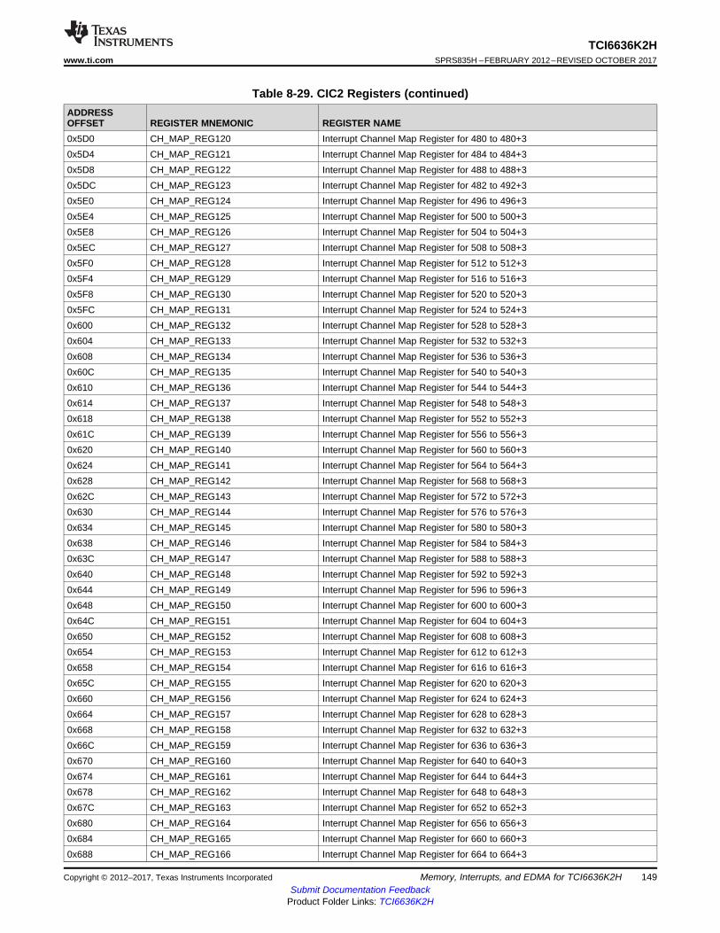
149
TCI6636K2Hwww.ti.com SPRS835H –FEBRUARY 2012–REVISED OCTOBER 2017
Submit Documentation FeedbackProduct Folder Links: TCI6636K2H
Memory, Interrupts, and EDMA for TCI6636K2HCopyright © 2012–2017, Texas Instruments Incorporated
Table 8-29. CIC2 Registers (continued)ADDRESSOFFSET REGISTER MNEMONIC REGISTER NAME0x5D0 CH_MAP_REG120 Interrupt Channel Map Register for 480 to 480+30x5D4 CH_MAP_REG121 Interrupt Channel Map Register for 484 to 484+30x5D8 CH_MAP_REG122 Interrupt Channel Map Register for 488 to 488+30x5DC CH_MAP_REG123 Interrupt Channel Map Register for 482 to 492+30x5E0 CH_MAP_REG124 Interrupt Channel Map Register for 496 to 496+30x5E4 CH_MAP_REG125 Interrupt Channel Map Register for 500 to 500+30x5E8 CH_MAP_REG126 Interrupt Channel Map Register for 504 to 504+30x5EC CH_MAP_REG127 Interrupt Channel Map Register for 508 to 508+30x5F0 CH_MAP_REG128 Interrupt Channel Map Register for 512 to 512+30x5F4 CH_MAP_REG129 Interrupt Channel Map Register for 516 to 516+30x5F8 CH_MAP_REG130 Interrupt Channel Map Register for 520 to 520+30x5FC CH_MAP_REG131 Interrupt Channel Map Register for 524 to 524+30x600 CH_MAP_REG132 Interrupt Channel Map Register for 528 to 528+30x604 CH_MAP_REG133 Interrupt Channel Map Register for 532 to 532+30x608 CH_MAP_REG134 Interrupt Channel Map Register for 536 to 536+30x60C CH_MAP_REG135 Interrupt Channel Map Register for 540 to 540+30x610 CH_MAP_REG136 Interrupt Channel Map Register for 544 to 544+30x614 CH_MAP_REG137 Interrupt Channel Map Register for 548 to 548+30x618 CH_MAP_REG138 Interrupt Channel Map Register for 552 to 552+30x61C CH_MAP_REG139 Interrupt Channel Map Register for 556 to 556+30x620 CH_MAP_REG140 Interrupt Channel Map Register for 560 to 560+30x624 CH_MAP_REG141 Interrupt Channel Map Register for 564 to 564+30x628 CH_MAP_REG142 Interrupt Channel Map Register for 568 to 568+30x62C CH_MAP_REG143 Interrupt Channel Map Register for 572 to 572+30x630 CH_MAP_REG144 Interrupt Channel Map Register for 576 to 576+30x634 CH_MAP_REG145 Interrupt Channel Map Register for 580 to 580+30x638 CH_MAP_REG146 Interrupt Channel Map Register for 584 to 584+30x63C CH_MAP_REG147 Interrupt Channel Map Register for 588 to 588+30x640 CH_MAP_REG148 Interrupt Channel Map Register for 592 to 592+30x644 CH_MAP_REG149 Interrupt Channel Map Register for 596 to 596+30x648 CH_MAP_REG150 Interrupt Channel Map Register for 600 to 600+30x64C CH_MAP_REG151 Interrupt Channel Map Register for 604 to 604+30x650 CH_MAP_REG152 Interrupt Channel Map Register for 608 to 608+30x654 CH_MAP_REG153 Interrupt Channel Map Register for 612 to 612+30x658 CH_MAP_REG154 Interrupt Channel Map Register for 616 to 616+30x65C CH_MAP_REG155 Interrupt Channel Map Register for 620 to 620+30x660 CH_MAP_REG156 Interrupt Channel Map Register for 624 to 624+30x664 CH_MAP_REG157 Interrupt Channel Map Register for 628 to 628+30x668 CH_MAP_REG158 Interrupt Channel Map Register for 632 to 632+30x66C CH_MAP_REG159 Interrupt Channel Map Register for 636 to 636+30x670 CH_MAP_REG160 Interrupt Channel Map Register for 640 to 640+30x674 CH_MAP_REG161 Interrupt Channel Map Register for 644 to 644+30x678 CH_MAP_REG162 Interrupt Channel Map Register for 648 to 648+30x67C CH_MAP_REG163 Interrupt Channel Map Register for 652 to 652+30x680 CH_MAP_REG164 Interrupt Channel Map Register for 656 to 656+30x684 CH_MAP_REG165 Interrupt Channel Map Register for 660 to 660+30x688 CH_MAP_REG166 Interrupt Channel Map Register for 664 to 664+3

150
TCI6636K2HSPRS835H –FEBRUARY 2012–REVISED OCTOBER 2017 www.ti.com
Submit Documentation FeedbackProduct Folder Links: TCI6636K2H
Memory, Interrupts, and EDMA for TCI6636K2H Copyright © 2012–2017, Texas Instruments Incorporated
Table 8-29. CIC2 Registers (continued)ADDRESSOFFSET REGISTER MNEMONIC REGISTER NAME0x68C CH_MAP_REG167 Interrupt Channel Map Register for 668 to 668+30x690 CH_MAP_REG168 Interrupt Channel Map Register for 672 to 672+30x694 CH_MAP_REG169 Interrupt Channel Map Register for 676 to 676+30x698 CH_MAP_REG170 Interrupt Channel Map Register for 680 to 680+30x69C CH_MAP_REG171 Interrupt Channel Map Register for 684 to 684+30x800 HINT_MAP_REG0 Host Interrupt Map Register for 0 to 0+30x804 HINT_MAP_REG1 Host Interrupt Map Register for 4 to 4+30x808 HINT_MAP_REG2 Host Interrupt Map Register for 8 to 8+30x80C HINT_MAP_REG3 Host Interrupt Map Register for 12 to 12+30x810 HINT_MAP_REG4 Host Interrupt Map Register for 16 to 16+30x814 HINT_MAP_REG5 Host Interrupt Map Register for 20 to 20+30x818 HINT_MAP_REG6 Host Interrupt Map Register for 24 to 24+30x81C HINT_MAP_REG7 Host Interrupt Map Register for 28 to 28+30x820 HINT_MAP_REG8 Host Interrupt Map Register for 32 to 32+30x824 HINT_MAP_REG9 Host Interrupt Map Register for 36 to 36+30x828 HINT_MAP_REG10 Host Interrupt Map Register for 40 to 40+30x82C HINT_MAP_REG11 Host Interrupt Map Register for 44 to 44+30x830 HINT_MAP_REG12 Host Interrupt Map Register for 48 to 48+30x834 HINT_MAP_REG13 Host Interrupt Map Register for 52 to 52+30x838 HINT_MAP_REG14 Host Interrupt Map Register for 56 to 56+30x83C HINT_MAP_REG15 Host Interrupt Map Register for 60 to 60+30x840 HINT_MAP_REG16 Host Interrupt Map Register for 63 to 63+30x844 HINT_MAP_REG17 Host Interrupt Map Register for 66 to 66+30x848 HINT_MAP_REG18 Host Interrupt Map Register for 68 to 68+30x84C HINT_MAP_REG19 Host Interrupt Map Register for 72 to 72+30x850 HINT_MAP_REG20 Host Interrupt Map Register for 76 to 76+30x854 HINT_MAP_REG21 Host Interrupt Map Register for 80 to 80+30x858 HINT_MAP_REG22 Host Interrupt Map Register for 84 to 84+30x85C HINT_MAP_REG23 Host Interrupt Map Register for 88 to 88+30x860 HINT_MAP_REG24 Host Interrupt Map Register for 92 to 92+30x864 HINT_MAP_REG25 Host Interrupt Map Register for 94 to 94+30x868 HINT_MAP_REG26 Host Interrupt Map Register for 96 to 96+30x86C HINT_MAP_REG27 Host Interrupt Map Register for 100 to 100+30x1500 ENABLE_HINT_REG0 Host Int Enable Register 00x1504 ENABLE_HINT_REG1 Host Int Enable Register 1
8.3.3 Inter-Processor Register Map
Table 8-30. IPC Generation Registers (IPCGRx)
ADDRESS START ADDRESS END SIZE REGISTER NAME DESCRIPTION0x02620200 0x02620203 4B NMIGR0 NMI Event Generation Register for C66x CorePac00x02620204 0x02620207 4B NMIGR1 NMI Event Generation Register for C66x CorePac10x02620208 0x0262020B 4B NMIGR2 NMI Event Generation Register for C66x CorePac20x0262020C 0x0262020F 4B NMIGR3 NMI Event Generation Register for C66x CorePac30x02620210 0x02620213 4B NMIGR4 NMI Event Generation Register for C66x CorePac40x02620214 0x02620217 4B NMIGR5 NMI Event Generation Register for C66x CorePac50x02620218 0x0262021B 4B NMIGR6 NMI Event Generation Register for C66x CorePac6

151
TCI6636K2Hwww.ti.com SPRS835H –FEBRUARY 2012–REVISED OCTOBER 2017
Submit Documentation FeedbackProduct Folder Links: TCI6636K2H
Memory, Interrupts, and EDMA for TCI6636K2HCopyright © 2012–2017, Texas Instruments Incorporated
Table 8-30. IPC Generation Registers (IPCGRx) (continued)ADDRESS START ADDRESS END SIZE REGISTER NAME DESCRIPTION0x0262021C 0x0262021F 4B NMIGR7 NMI Event Generation Register for C66x CorePac70x02620220 0x0262023F 32B Reserved Reserved0x02620240 0x02620243 4B IPCGR0 IPC Generation Register for C66x CorePac00x02620244 0x02620247 4B IPCGR1 IPC Generation Register for C66x CorePac10x02620248 0x0262024B 4B IPCGR2 IPC Generation Register for C66x CorePac20x0262024C 0x0262024F 4B IPCGR3 IPC Generation Register for C66x CorePac30x02620250 0x02620253 4B IPCGR4 IPC Generation Register for C66x CorePac40x02620254 0x02620257 4B IPCGR5 IPC Generation Register for C66x CorePac50x02620258 0x0262025B 4B IPCGR6 IPC Generation Register for C66x CorePac60x0262025C 0x0262025F 4B IPCGR7 IPC Generation Register for C66x CorePac70x02620260 0x02620263 4B IPCGR8 IPC Generation Register for ARM CorePac00x02620264 0x02620267 4B IPCGR9 IPC Generation Register for ARM CorePac10x02620268 0x0262026B 4B IPCGR10 IPC Generation Register for ARM CorePac20x0262026C 0x0262026F 4B IPCGR11 IPC Generation Register for ARM CorePac30x02620270 0x0262027B 12B Reserved Reserved0x0262027C 0x0262027F 4B IPCGRH IPC Generation Register for Host0x02620280 0x02620283 4B IPCAR0 IPC Acknowledgment Register for C66x CorePac00x02620284 0x02620287 4B IPCAR1 IPC Acknowledgment Register for C66x CorePac10x02620288 0x0262028B 4B IPCAR2 IPC Acknowledgment Register for C66x CorePac20x0262028C 0x0262028F 4B IPCAR3 IPC Acknowledgment Register for C66x CorePac30x02620290 0x02620293 4B IPCAR4 IPC Acknowledgment Register for C66x CorePac40x02620294 0x02620297 4B IPCAR5 IPC Acknowledgment Register for C66x CorePac50x02620298 0x0262029B 4B IPCAR6 IPC Acknowledgment Register for C66x CorePac60x0262029C 0x0262029F 4B IPCAR7 IPC Acknowledgment Register for C66x CorePac70x026202A0 0x026202A3 4B IPCAR8 IPC Acknowledgment Register for ARM CorePac00x026202A4 0x026202A7 4B IPCAR9 IPC Acknowledgement Register for ARM CorePac10x026202A8 0x026202AB 4B IPCAR10 IPC Acknowledgment Register for ARM CorePac20x026202AC 0x026202AF 4B IPCAR11 IPC Acknowledgment Register for ARM CorePac30x026202B0 0x026202BB 12B Reserved Reserved0x026202A0 0x026202BB 28B Reserved Reserved0x026202BC 0x026202BF 4B IPCARH IPC Acknowledgment Register for host
8.3.4 NMI and LRESETThe Nonmaskable Interrupts (NMI) can be generated by chip-level registers and the LRESET can begenerated by software writing into LPSC registers. LRESET and NMI can also be asserted by device pinsor watchdog timers. One NMI pin and one LRESET pin are shared by all eight C66x CorePacs on thedevice. The CORESEL[3:0] pins can be configured to select between the eight C66x CorePacs availableas shown in Table 8-31.
Table 8-31. LRESET and NMI Decoding
CORESEL[3:0] PININPUT
LRESET PININPUT
NMI PININPUT
LRESETNMIEN PININPUT RESET MUX BLOCK OUTPUT
XXXX X X 1 No local reset or NMI assertion0000 0 X 0 Assert local reset to C66x CorePac00001 0 X 0 Assert local reset to C66x CorePac10010 0 X 0 Assert local reset to C66x CorePac20011 0 X 0 Assert local reset to C66x CorePac30100 0 X 0 Assert local reset to C66x CorePac4

152
TCI6636K2HSPRS835H –FEBRUARY 2012–REVISED OCTOBER 2017 www.ti.com
Submit Documentation FeedbackProduct Folder Links: TCI6636K2H
Memory, Interrupts, and EDMA for TCI6636K2H Copyright © 2012–2017, Texas Instruments Incorporated
Table 8-31. LRESET and NMI Decoding (continued)CORESEL[3:0] PININPUT
LRESET PININPUT
NMI PININPUT
LRESETNMIEN PININPUT RESET MUX BLOCK OUTPUT
0101 0 X 0 Assert local reset to C66x CorePac50110 0 X 0 Assert local reset to C66x CorePac60111 0 X 0 Assert local reset to C66x CorePac71XXX 0 X 0 Assert local reset to all C66x CorePacs0000 1 1 0 Deassert local reset & NMI to C66x CorePac00001 1 1 0 Deassert local reset & NMI to C66x CorePac10010 1 1 0 Deassert local reset & NMI to C66x CorePac20011 1 1 0 Deassert local reset & NMI to C66x CorePac30100 1 1 0 Deassert local reset & NMI to C66x CorePac40101 1 1 0 Deassert local reset & NMI to C66x CorePac50110 1 1 0 Deassert local reset & NMI to C66x CorePac60111 1 1 0 Deassert local reset & NMI to C66x CorePac71XXX 1 1 0 Deassert local reset & NMI to all C66x CorePacs0000 1 0 0 Assert NMI to C66x CorePac00001 1 0 0 Assert NMI to C66x CorePac10010 1 0 0 Assert NMI to C66x CorePac20011 1 0 0 Assert NMI to C66x CorePac30100 1 0 0 Assert NMI to C66x CorePac40101 1 0 0 Assert NMI to C66x CorePac50110 1 0 0 Assert NMI to C66x CorePac60111 1 0 0 Assert NMI to C66x CorePac71XXX 1 0 0 Assert NMI to all C66x CorePacs
8.4 Enhanced Direct Memory Access (EDMA3) Controller for TCI6636K2HThe primary purpose of the EDMA3 is to service user-programmed data transfers between two memory-mapped slave endpoints on the device. The EDMA3 services software-driven paging transfers (forexample, data movement between external memory and internal memory), performs sorting or subframeextraction of various data structures, services event driven peripherals, and offloads data transfers fromthe device C66x DSP CorePac or the ARM CorePac.
There are five EDMA channel controllers on the device:• EDMA3CC0 has two transfer controllers: TPTC0 and TPTC1• EDMA3CC1 has four transfer controllers: TPTC0, TPTC1, TPTC2, and TPTC3• EDMA3CC2 has four transfer controllers: TPTC0, TPTC1, TPTC2, and TPTC3• EDMA3CC3 has two transfer controllers: TPTC0 and TPTC1• EDMA3CC4 has two transfer controllers: TPTC0 and TPTC1
In the context of this document, TPTCx is associated with EDMA3CCy, and is referred to as EDMA3CCyTPTCx. Each of the transfer controllers has a direct connection to the switch fabric. Section 9.2 lists theperipherals that can be accessed by the transfer controllers.
EDMA3CC0 is optimized to be used for transfers to/from/within the MSMC and DDR3A subsystems. Theothers are used for the remaining traffic.
Each EDMA3 channel controller includes the following features:

153
TCI6636K2Hwww.ti.com SPRS835H –FEBRUARY 2012–REVISED OCTOBER 2017
Submit Documentation FeedbackProduct Folder Links: TCI6636K2H
Memory, Interrupts, and EDMA for TCI6636K2HCopyright © 2012–2017, Texas Instruments Incorporated
• Fully orthogonal transfer description– 3 transfer dimensions:
• Array (multiple bytes)• Frame (multiple arrays)• Block (multiple frames)
– Single event can trigger transfer of array, frame, or entire block– Independent indexes on source and destination
• Flexible transfer definition:– Increment or FIFO transfer addressing modes– Linking mechanism allows for ping-pong buffering, circular buffering, and repetitive/continuous
transfers, all with no CPU intervention– Chaining allows multiple transfers to execute with one event
• 512 PaRAM entries for all EDMA3CC– Used to define transfer context for channels– Each PaRAM entry can be used as a DMA entry, QDMA entry, or link entry
• 64 DMA channels for all EDMA3CC– Manually triggered (CPU writes to channel controller register)– External event triggered– Chain triggered (completion of one transfer triggers another)
• 8 Quick DMA (QDMA) channels per EDMA3CCx– Used for software-driven transfers– Triggered upon writing to a single PaRAM set entry
• Two transfer controllers and two event queues with programmable system-level priority forEDMA3CC0, EDMA3CC3 and EDMA3CC4
• Four transfer controllers and four event queues with programmable system-level priority for each ofEDMA3CC1 and EDMA3CC2
• Interrupt generation for transfer completion and error conditions• Debug visibility
– Queue watermarking/threshold allows detection of maximum usage of event queues– Error and status recording to facilitate debug
8.4.1 EDMA3 Device-Specific InformationThe EDMA supports two addressing modes: constant addressing and increment addressing mode.Constant addressing mode is applicable to a very limited set of use cases. For most applicationsincrement mode can be used. On the TCI6636K2H SoC, the EDMA can use constant addressing modeonly with the enhanced Viterbi decoder coprocessor (VCP) and the enhanced turbo decoder coprocessor(TCP). Constant addressing mode is not supported by any other peripheral or internal memory in the DSP.Note that increment mode is supported by all peripherals, including VCP and TCP. For more informationon these two addressing modes, see the KeyStone Architecture Enhanced Direct Memory Access 3(EDMA3) User's Guide.
For the range of memory addresses that includes EDMA3 channel controller (EDMA3CC) control registersand EDMA3 transfer controller (TPTC) control registers, see Section Section 8.1. For memory offsets andother details on EDMA3CC and TPTC Control Register entries, see the KeyStone Architecture EnhancedDirect Memory Access 3 (EDMA3) User's Guide.
8.4.2 EDMA3 Channel Controller ConfigurationTable 8-32 shows the configuration for each of the EDMA3 channel controllers present on the device.

154
TCI6636K2HSPRS835H –FEBRUARY 2012–REVISED OCTOBER 2017 www.ti.com
Submit Documentation FeedbackProduct Folder Links: TCI6636K2H
Memory, Interrupts, and EDMA for TCI6636K2H Copyright © 2012–2017, Texas Instruments Incorporated
Table 8-32. EDMA3 Channel Controller Configuration
DESCRIPTION EDMA3 CC0 EDMA3 CC1 EDMA3 CC2 EDMA3 CC3 EDMA3 CC4Number of DMA channels in channel controller 64 64 64 64 64Number of QDMA channels 8 8 8 8 8Number of interrupt channels 64 64 64 64 64Number of PaRAM set entries 512 512 512 512 512Number of event queues 2 4 4 2 2Number of transfer controllers 2 4 4 2 2Memory protection existence Yes Yes Yes Yes YesNumber of memory protection and shadow regions 8 8 8 8 8
8.4.3 EDMA3 Transfer Controller ConfigurationEach transfer controller on the device is designed differently based on considerations like performancerequirements, system topology (like main TeraNet bus width, external memory bus width), and so forth.The parameters that determine the transfer controller configurations are:• FIFOSIZE: Determines the size in bytes for the data FIFO that is the temporary buffer for the in-flight
data. The data FIFO is where the read return data read by the TC read controller from the sourceendpoint is stored and subsequently written out to the destination endpoint by the TC write controller.
• BUSWIDTH: The width of the read and write data buses in bytes, for the TC read and write controller,respectively. This is typically equal to the bus width of the main TeraNet interface.
• Default Burst Size (DBS): The DBS is the maximum number of bytes per read/write command issuedby a transfer controller.
• DSTREGDEPTH: This determines the number of destination FIFO register sets. The number ofdestination FIFO register sets for a transfer controller determines the maximum number of outstandingtransfer requests.
All four parameters listed above are fixed by the design of the device.
Table 8-33 shows the configuration of each of the EDMA3 transfer controllers present on the device.
Table 8-33. EDMA3 Transfer Controller Configuration
PARAMETEREDMA3 CC0/CC4 EDMA3 CC1 EDMA3 CC2 EDMA3CC3TC0 TC1 TC0 TC1 TC2 TC3 TC0 TC1 TC2 TC3 TC0 TC1
FIFOSIZE 1024bytes
1024bytes
1024bytes
1024bytes
1024bytes
1024bytes
1024bytes
1024bytes
1024bytes
1024bytes
1024bytes
1024bytes
BUSWIDTH 32bytes
32bytes
16bytes
16bytes
16bytes
16bytes
16bytes
16bytes
16bytes
16bytes
16bytes
16bytes
DSTREGDEPTH 4entries
4entries
4entries
4entries
4entries
4entries
4entries
4entries
4entries
4entries
4entries
4entries
DBS 128bytes
128bytes
128bytes
128bytes
128bytes
128bytes
128bytes
128bytes
128bytes
128bytes
64bytes
64bytes
8.4.4 EDMA3 Channel Synchronization EventsThe EDMA3 supports up to 64 DMA channels for all EDMA3CC that can be used to service systemperipherals and to move data between system memories. DMA channels can be triggered bysynchronization events generated by system peripherals. The following tables list the source of thesynchronization event associated with each of the EDMA3CC DMA channels. On the TCI6636K2H, theassociation of each synchronization event and DMA channel is fixed and cannot be reprogrammed.
For more detailed information on the EDMA3 module and how EDMA3 events are enabled, captured,processed, prioritized, linked, chained, and cleared, and so forth, see the KeyStone ArchitectureEnhanced Direct Memory Access 3 (EDMA3) User's Guide.

155
TCI6636K2Hwww.ti.com SPRS835H –FEBRUARY 2012–REVISED OCTOBER 2017
Submit Documentation FeedbackProduct Folder Links: TCI6636K2H
Memory, Interrupts, and EDMA for TCI6636K2HCopyright © 2012–2017, Texas Instruments Incorporated
Table 8-34. EDMA3CC0 Events for TCI6636K2H
EVENTNO. EVENT NAME DESCRIPTION0 TIMER_8_INTL Timer interrupt low1 TIMER_8_INTH Timer interrupt high2 TIMER_9_INTL Timer interrupt low3 TIMER_9_INTH Timer interrupt high4 TIMER_10_INTL Timer interrupt low5 TIMER_10_INTH Timer interrupt high6 TIMER_11_INTL Timer interrupt low7 TIMER_11_INTH Timer interrupt high8 CIC_2_OUT66 CIC2 Interrupt Controller output9 CIC_2_OUT67 CIC2 Interrupt Controller output10 CIC_2_OUT68 CIC2 Interrupt Controller output11 CIC_2_OUT69 CIC2 Interrupt Controller output12 CIC_2_OUT70 CIC2 Interrupt Controller output13 CIC_2_OUT71 CIC2 Interrupt Controller output14 CIC_2_OUT72 CIC2 Interrupt Controller output15 CIC_2_OUT73 CIC2 Interrupt Controller output16 GPIO_INT8 GPIO interrupt17 GPIO_INT9 GPIO interrupt18 GPIO_INT10 GPIO interrupt19 GPIO_INT11 GPIO interrupt20 GPIO_INT12 GPIO interrupt21 GPIO_INT13 GPIO interrupt22 GPIO_INT14 GPIO interrupt23 GPIO_INT15 GPIO interrupt24 TIMER_4_INTL Timer interrupt low25 TIMER_4_INTH Timer interrupt high26 TIMER_5_INTL Timer interrupt low27 TIMER_5_INTH Timer interrupt high28 TIMER_6_INTL Timer interrupt low29 TIMER_6_INTH Timer interrupt high30 TIMER_7_INTL Timer interrupt low31 TIMER_7_INTH Timer interrupt high32 GPIO_INT0 GPIO interrupt33 GPIO_INT1 GPIO interrupt34 GPIO_INT2 GPIO interrupt35 GPIO_INT3 GPIO interrupt36 GPIO_INT4 GPIO interrupt37 GPIO_INT5 GPIO interrupt38 GPIO_INT6 GPIO interrupt39 GPIO_INT7 GPIO interrupt40 TIMER_0_INTL Timer interrupt low41 TIMER_0_INTH Timer interrupt high42 TIMER_1_INTL Timer interrupt low43 TIMER_1_INTH Timer interrupt high44 TIMER_2_INTL Timer interrupt low45 TIMER_2_INTH Timer interrupt high

156
TCI6636K2HSPRS835H –FEBRUARY 2012–REVISED OCTOBER 2017 www.ti.com
Submit Documentation FeedbackProduct Folder Links: TCI6636K2H
Memory, Interrupts, and EDMA for TCI6636K2H Copyright © 2012–2017, Texas Instruments Incorporated
Table 8-34. EDMA3CC0 Events for TCI6636K2H (continued)EVENTNO. EVENT NAME DESCRIPTION46 TIMER_3_INTL Timer interrupt low47 TIMER_3_INTH Timer interrupt high48 SRIO_INTDST0 SRIO interrupt49 SRIO_INTDST1 SRIO interrupt50 SRIO_INTDST2 SRIO interrupt51 SRIO_INTDST3 SRIO interrupt52 SRIO_INTDST4 SRIO interrupt53 SRIO_INTDST5 SRIO interrupt54 SRIO_INTDST6 SRIO interrupt55 SRIO_INTDST7 SRIO interrupt56 AIF_ATEVT0 AIF timer57 AIF_ATEVT1 AIF timer58 AIF_ATEVT2 AIF timer59 AIF_ATEVT3 AIF timer60 AIF_ATEVT4 AIF timer61 AIF_ATEVT5 AIF timer62 AIF_ATEVT6 AIF timer63 AIF_ATEVT7 AIF timer
Table 8-35. EDMA3CC1 Events for TCI6636K2H
EVENTNO. EVENT NAME DESCRIPTION0 SPI_0_INT0 SPI0 interrupt1 SPI_0_INT1 SPI0 interrupt2 SPI_0_XEVT SPI0 transmit event3 SPI_0_REVT SPI0 receive event4 SEM_INT8 Semaphore interrupt5 SEM_INT9 Semaphore interrupt6 GPIO_INT0 GPIO interrupt7 GPIO_INT1 GPIO interrupt8 GPIO_INT2 GPIO interrupt9 GPIO_INT3 GPIO interrupt10 AIF_ATEVT0 AIF Timer event11 AIF_ATEVT1 AIF Timer event12 AIF_ATEVT2 AIF Timer event13 AIF_ATEVT3 AIF Timer event14 SEM_INT0 Semaphore interrupt15 SEM_INT1 Semaphore interrupt16 SEM_INT2 Semaphore interrupt17 SEM_INT3 Semaphore interrupt18 SEM_INT4 Semaphore interrupt19 SEM_INT5 Semaphore interrupt20 SEM_INT6 Semaphore interrupt21 SEM_INT7 Semaphore interrupt22 TIMER_8_INTL Timer interrupt low23 TIMER_8_INTH Timer interrupt high24 TIMER_9_INTL Timer interrupt low

157
TCI6636K2Hwww.ti.com SPRS835H –FEBRUARY 2012–REVISED OCTOBER 2017
Submit Documentation FeedbackProduct Folder Links: TCI6636K2H
Memory, Interrupts, and EDMA for TCI6636K2HCopyright © 2012–2017, Texas Instruments Incorporated
Table 8-35. EDMA3CC1 Events for TCI6636K2H (continued)EVENTNO. EVENT NAME DESCRIPTION25 TIMER_9_INTH Timer interrupt high26 TIMER_10_INTL Timer interrupt low27 TIMER_10_INTH Timer interrupt high28 TIMER_11_INTL Timer interrupt low29 TIMER_11_INTH Timer interrupt high30 TIMER_12_INTL Timer interrupt low31 TIMER_12_INTH Timer interrupt high32 TIMER_13_INTL Timer interrupt low33 TIMER_13_INTH Timer interrupt high34 TIMER_14_INTL Timer interrupt low35 TIMER_14_INTH Timer interrupt high36 TIMER_15_INTL Timer interrupt low37 TIMER_15_INTH Timer interrupt high38 SEM_INT10 Semaphore interrupt39 SEM_INT11 Semaphore interrupt40 SEM_INT12 Semaphore interrupt41 SEM_INT13 Semaphore interrupt42 CIC_2_OUT0 CIC2 Interrupt Controller output43 CIC_2_OUT1 CIC2 Interrupt Controller output44 CIC_2_OUT2 CIC2 Interrupt Controller output45 CIC_2_OUT3 CIC2 Interrupt Controller output46 CIC_2_OUT4 CIC2 Interrupt Controller output47 CIC_2_OUT5 CIC2 Interrupt Controller output48 CIC_2_OUT6 CIC2 Interrupt Controller output49 CIC_2_OUT7 CIC2 Interrupt Controller output50 CIC_2_OUT8 CIC2 Interrupt Controller output51 AIF_ATEVT4 AIF Timer event52 AIF_ATEVT5 AIF Timer event53 I2C_0_REVT I2C0 receive54 I2C_0_XEVT I2C0 transmit55 CIC_2_OUT13 CIC2 Interrupt Controller output56 CIC_2_OUT14 CIC2 Interrupt Controller output57 CIC_2_OUT15 CIC2 Interrupt Controller output58 CIC_2_OUT16 CIC2 Interrupt Controller output59 CIC_2_OUT17 CIC2 Interrupt Controller output60 CIC_2_OUT18 CIC2 Interrupt Controller output61 CIC_2_OUT19 CIC2 Interrupt Controller output62 USIM_RREQ USIM read DMA event63 USIM_WREQ USIM write DMA event
Table 8-36. EDMA3CC2 Events for TCI6636K2H
EVENTNO. EVENT NAME DESCRIPTION0 TAC_DEVT2 TAC debug1 TAC_DEVT3 TAC debug2 TAC_DEVT4 TAC debug3 TAC_DEVT5 TAC debug

158
TCI6636K2HSPRS835H –FEBRUARY 2012–REVISED OCTOBER 2017 www.ti.com
Submit Documentation FeedbackProduct Folder Links: TCI6636K2H
Memory, Interrupts, and EDMA for TCI6636K2H Copyright © 2012–2017, Texas Instruments Incorporated
Table 8-36. EDMA3CC2 Events for TCI6636K2H (continued)EVENTNO. EVENT NAME DESCRIPTION4 AIF_ATEVT4 AIF timer5 AIF_ATEVT5 AIF timer6 TETB_FULLINT4 TETB4 is full7 TETB_HFULLINT4 TETB4 is half full8 TETB_FULLINT5 TETB5 is full9 TETB_HFULLINT5 TETB5 is half full10 TETB_FULLINT6 TETB6 is full11 TETB_HFULLINT6 TETB6 is half full12 TETB_FULLINT7 TETB7 is full13 TETB_HFULLINT7 TETB7 is half full14 SRIO_INTDST0 SRIO interrupt15 SRIO_INTDST1 SRIO interrupt16 SRIO_INTDST2 SRIO interrupt17 SRIO_INTDST3 SRIO interrupt18 SRIO_INTDST4 SRIO interrupt19 SRIO_INTDST5 SRIO interrupt20 SRIO_INTDST6 SRIO interrupt21 SRIO_INTDST7 SRIO interrupt22 AIF_ATEVT6 AIF timer23 AIF_ATEVT7 AIF timer24 TAC_DEVT0 TAC debug25 TAC_DEVT1 TAC debug26 GPIO_INT0 GPIO interrupt27 GPIO_INT1 GPIO interrupt28 GPIO_INT2 GPIO interrupt29 GPIO_INT3 GPIO interrupt30 GPIO_INT4 GPIO interrupt31 GPIO_INT5 GPIO interrupt32 GPIO_INT6 GPIO interrupt33 GPIO_INT7 GPIO interrupt34 TCP3D_0_REVT0 TCP3d event35 TCP3D_0_REVT1 TCP3d event36 TCP3D_1_REVT0 TCP3d event37 TCP3D_1_REVT1 TCP3d event38 CIC_2_OUT48 CIC2 Interrupt Controller output39 TAC_INT TAC interrupt40 UART_0_URXEVT UART0 receive event41 UART_0_UTXEVT UART0 transmit event42 CIC_2_OUT22 CIC2 Interrupt Controller output43 CIC_2_OUT23 CIC2 Interrupt Controller output44 CIC_2_OUT24 CIC2 Interrupt Controller output45 CIC_2_OUT25 CIC2 Interrupt Controller output46 CIC_2_OUT26 CIC2 Interrupt Controller output47 CIC_2_OUT27 CIC2 Interrupt Controller output48 CIC_2_OUT28 CIC2 Interrupt Controller output49 SPI_0_XEVT SPI0 transmit event50 SPI_0_REVT SPI0 receive event

159
TCI6636K2Hwww.ti.com SPRS835H –FEBRUARY 2012–REVISED OCTOBER 2017
Submit Documentation FeedbackProduct Folder Links: TCI6636K2H
Memory, Interrupts, and EDMA for TCI6636K2HCopyright © 2012–2017, Texas Instruments Incorporated
Table 8-36. EDMA3CC2 Events for TCI6636K2H (continued)EVENTNO. EVENT NAME DESCRIPTION51 VCP_0_REVT0 VCP receive event52 VCP_0_XEVT0 VCP transmit event53 VCP_0_REVT1 VCP receive event54 VCP_0_XEVT1 VCP transmit event55 VCP_0_REVT2 VCP receive event56 VCP_0_XEVT2 VCP transmit event57 VCP_0_REVT3 VCP receive event58 VCP_0_XEVT3 VCP transmit event59 RAC_0_INT RAC interrupt60 RAC_1_INT RAC interrupt61 Reserved Reserved62 Reserved Reserved63 BCP_INT0 BCP interrupt
Table 8-37. EDMA3CC3 Events for TCI6636K2H
EVENTNO. EVENT NAME DESCRIPTION0 SPI_2_INT0 SPI2 interrupt1 SPI_2_INT1 SPI2 interrupt2 SPI_2_XEVT SPI2 transmit event3 SPI_2_REVT SPI2 receive event4 I2C_2_REVT I2C2 receive5 I2C_2_XEVT I2C2 transmit6 UART_1_URXEVT UART1 receive event7 UART_1_UTXEVT UART1 transmit event8 SPI_1_INT0 SPI1 interrupt9 SPI_1_INT1 SPI1 interrupt10 SPI_1_XEVT SPI1 transmit event11 SPI_1_REVT SPI1 receive event12 I2C_0_REVT I2C0 receive13 I2C_0_XEVT I2C0 transmit14 I2C_1_REVT I2C1 receive15 I2C_1_XEVT I2C1 transmit16 SRIO_INTDST0 SRIO interrupt17 SRIO_INTDST1 SRIO interrupt18 SRIO_INTDST2 SRIO interrupt19 SRIO_INTDST3 SRIO interrupt20 SRIO_INTDST4 SRIO interrupt21 SRIO_INTDST5 SRIO interrupt22 SRIO_INTDST6 SRIO interrupt23 SRIO_INTDST7 SRIO interrupt24 TCP3D_0_REVT0 TCP3d event25 TCP3D_0_REVT1 TCP3d event26 TCP3D_1_REVT0 TCP3d event27 TCP3D_1_REVT1 TCP3d event28 Reserved Reserved29 Reserved Reserved

160
TCI6636K2HSPRS835H –FEBRUARY 2012–REVISED OCTOBER 2017 www.ti.com
Submit Documentation FeedbackProduct Folder Links: TCI6636K2H
Memory, Interrupts, and EDMA for TCI6636K2H Copyright © 2012–2017, Texas Instruments Incorporated
Table 8-37. EDMA3CC3 Events for TCI6636K2H (continued)EVENTNO. EVENT NAME DESCRIPTION30 Reserved Reserved31 Reserved Reserved32 TETB_FULLINT0 TETB0 is full33 TETB_HFULLINT0 TETB0 is half full34 TETB_FULLINT1 TETB1 is full35 TETB_HFULLINT1 TETB1 is half full36 TETB_FULLINT2 TETB2 is full37 TETB_HFULLINT2 TETB2 is half full38 TETB_FULLINT3 TETB3 is full39 TETB_HFULLINT3 TETB3 is half full40 VCP_0_REVT0 VCP event41 VCP_0_XEVT0 VCP event42 VCP_0_REVT1 VCP event43 VCP_0_XEVT1 VCP event44 VCP_0_REVT2 VCP event45 VCP_0_XEVT2 VCP event46 VCP_0_REVT3 VCP event47 VCP_0_XEVT3 VCP event48 VCP_1_REVT0 VCP event49 VCP_1_XEVT0 VCP event50 VCP_1_REVT1 VCP event51 VCP_1_XEVT1 VCP event52 VCP_1_REVT2 VCP event53 VCP_1_XEVT2 VCP event54 VCP_1_REVT3 VCP event55 VCP_1_XEVT3 VCP event56 CIC_2_OUT57 CIC2 Interrupt Controller output57 CIC_2_OUT50 CIC2 Interrupt Controller output58 CIC_2_OUT51 CIC2 Interrupt Controller output59 CIC_2_OUT52 CIC2 Interrupt Controller output60 CIC_2_OUT53 CIC2 Interrupt Controller output61 CIC_2_OUT54 CIC2 Interrupt Controller output62 CIC_2_OUT55 CIC2 Interrupt Controller output63 CIC_2_OUT56 CIC2 Interrupt Controller output
Table 8-38. EDMA3CC4 Events for TCI6636K2H
EVENT NO. EVENT NAME DESCRIPTION0 GPIO_INT16 GPIO interrupt1 GPIO_INT17 GPIO interrupt2 GPIO_INT18 GPIO interrupt3 GPIO_INT19 GPIO interrupt4 GPIO_INT20 GPIO interrupt5 GPIO_INT21 GPIO interrupt6 GPIO_INT22 GPIO interrupt7 GPIO_INT23 GPIO interrupt8 AIF_ATEVT0 AIF timer

161
TCI6636K2Hwww.ti.com SPRS835H –FEBRUARY 2012–REVISED OCTOBER 2017
Submit Documentation FeedbackProduct Folder Links: TCI6636K2H
Memory, Interrupts, and EDMA for TCI6636K2HCopyright © 2012–2017, Texas Instruments Incorporated
Table 8-38. EDMA3CC4 Events for TCI6636K2H (continued)EVENT NO. EVENT NAME DESCRIPTION9 AIF_ATEVT1 AIF timer10 AIF_ATEVT2 AIF timer11 AIF_ATEVT3 AIF timer12 AIF_ATEVT4 AIF timer13 AIF_ATEVT5 AIF timer14 AIF_ATEVT6 AIF timer15 AIF_ATEVT7 AIF timer16 AIF_ATEVT16 AIF timer17 AIF_ATEVT17 AIF timer18 AIF_ATEVT18 AIF timer19 AIF_ATEVT19 AIF timer20 AIF_ATEVT20 AIF timer21 AIF_ATEVT21 AIF timer22 AIF_ATEVT22 AIF timer23 AIF_ATEVT23 AIF timer24 TIMER_8_INTL Timer interrupt low25 TIMER_8_INTH Timer interrupt high26 TIMER_14_INTL Timer interrupt low27 TIMER_14_INTH Timer interrupt high28 TIMER_15_INTL Timer interrupt low29 TIMER_15_INTH Timer interrupt high30 DBGTBR_DMAINT Debug trace buffer (TBR) DMA event31 ARM_TBR_DMA ARM trace buffer (TBR) DMA event32 QMSS_QUE_PEND_658 Navigator transmit queue pending event for indicated queue33 QMSS_QUE_PEND_659 Navigator transmit queue pending event for indicated queue34 QMSS_QUE_PEND_660 Navigator transmit queue pending event for indicated queue35 QMSS_QUE_PEND_661 Navigator transmit queue pending event for indicated queue36 QMSS_QUE_PEND_662 Navigator transmit queue pending event for indicated queue37 QMSS_QUE_PEND_663 Navigator transmit queue pending event for indicated queue38 QMSS_QUE_PEND_664 Navigator transmit queue pending event for indicated queue39 QMSS_QUE_PEND_665 Navigator transmit queue pending event for indicated queue40 QMSS_QUE_PEND_8736 Navigator transmit queue pending event for indicated queue41 QMSS_QUE_PEND_8737 Navigator transmit queue pending event for indicated queue42 QMSS_QUE_PEND_8738 Navigator transmit queue pending event for indicated queue43 QMSS_QUE_PEND_8739 Navigator transmit queue pending event for indicated queue44 QMSS_QUE_PEND_8740 Navigator transmit queue pending event for indicated queue45 QMSS_QUE_PEND_8741 Navigator transmit queue pending event for indicated queue46 QMSS_QUE_PEND_8742 Navigator transmit queue pending event for indicated queue47 QMSS_QUE_PEND_8743 Navigator transmit queue pending event for indicated queue48 ARM_NCNTVIRQ3 ARM virtual timer interrupt for core 349 ARM_NCNTVIRQ2 ARM virtual timer interrupt for core 250 ARM_NCNTVIRQ1 ARM virtual timer interrupt for core 151 ARM_NCNTVIRQ0 ARM virtual timer interrupt for core 052 ARM_NCNTPNSIRQ3 ARM non secure timer interrupt for core 353 ARM_NCNTPNSIRQ2 ARM non secure timer interrupt for core 254 ARM_NCNTPNSIRQ1 ARM non secure timer interrupt for core 155 ARM_NCNTPNSIRQ0 ARM non secure timer interrupt for core 0

162
TCI6636K2HSPRS835H –FEBRUARY 2012–REVISED OCTOBER 2017 www.ti.com
Submit Documentation FeedbackProduct Folder Links: TCI6636K2H
Memory, Interrupts, and EDMA for TCI6636K2H Copyright © 2012–2017, Texas Instruments Incorporated
Table 8-38. EDMA3CC4 Events for TCI6636K2H (continued)EVENT NO. EVENT NAME DESCRIPTION56 CIC_2_OUT82 CIC2 Interrupt Controller output57 CIC_2_OUT83 CIC2 Interrupt Controller output58 CIC_2_OUT84 CIC2 Interrupt Controller output59 CIC_2_OUT85 CIC2 Interrupt Controller output60 CIC_2_OUT86 CIC2 Interrupt Controller output61 CIC_2_OUT87 CIC2 Interrupt Controller output62 CIC_2_OUT88 CIC2 Interrupt Controller output63 CIC_2_OUT89 CIC2 Interrupt Controller output

163
TCI6636K2Hwww.ti.com SPRS835H –FEBRUARY 2012–REVISED OCTOBER 2017
Submit Documentation FeedbackProduct Folder Links: TCI6636K2H
System InterconnectCopyright © 2012–2017, Texas Instruments Incorporated
9 System Interconnect
On the KeyStone II devices, the C66x CorePac, the EDMA3 transfer controllers and the systemperipherals are interconnected through the TeraNets, which are nonblocking switch fabrics enabling fastand contention-free internal data movement. The TeraNets provide low-latency, concurrent data transfersbetween master peripherals and slave peripherals. The TeraNets also allow for seamless arbitrationbetween the system masters when accessing system slaves.
The ARM CorePac is connected to the MSMC and the debug subsystem directly, and to other masters viathe TeraNets. Through the MSMC, the ARM CorePacs can be interconnected to DDR3A and TeraNet3_A, which allows the ARM CorePacs to access to the peripheral buses:• TeraNet 3P_A for peripheral configuration• TeraNet 6P_A for ARM• Boot ROM
9.1 Internal Buses and Switch FabricsThe C66x CorePacs, the ARM CorePacs, the EDMA3 traffic controllers, and the various systemperipherals can be classified into two categories: masters and slaves.• Masters are capable of initiating read and write transfers in the system and do not rely on the EDMA3
for their data transfers.• Slaves on the other hand rely on the masters to perform transfers to and from them.
Examples of masters include the EDMA3 traffic controllers and network coprocessor packet DMA.
Examples of slaves include the SPI, UART, and I2C.
The masters and slaves in the device communicate through the TeraNet (switch fabric). The devicecontains two types of switch fabric:• Data TeraNet is a high-throughput interconnect mainly used to move data across the system• Configuration TeraNet is mainly used to access peripheral registers
Some peripherals have both a data bus and a configuration bus interface, while others only have one typeof interface. Furthermore, the bus interface width and speed varies from peripheral to peripheral.
Note that the data TeraNet also connects to the configuration TeraNet.
9.2 Switch Fabric Connections Matrix - Data SpaceFigure 9-1, Figure 9-2, Figure 9-3, and Figure 9-4 show the connections between masters and slavesthrough various sections of the TeraNet.

Tera
Net
3_A
-1 C
PU
/3
SRIOPacket DMA M
QM_2Packet DMA M
FFTC_3Packet DMA M
Bridge_1
Bridge_2
Bridge_3
From TeraNet_3_C
Bridge_5
Bridge_6
Bridge_7
Bridge_8
To TeraNet_3_C
Bridge_9
Bridge_10
Bridge_12
Bridge_13
Bridge_14
To TeraNet_3P_A
TNet_3_GCPU/3
USB_MST M
BCP_DIO1 M
TNet_3_FCPU/3
TAC_FE M
TAC_FE2 M
TAC_FE3 M
TNet_3_DCPU/3
Debug_SS M
BCP_DIO0 M
FFTC_0Packet DMA M
FFTC_2Packet DMA M
FFTC_1Packet DMA M
QMPacket DMA M
BCPPacket DMA M
VCP2_3S
VCP2_2S
VCP2_1S
VCP2_0S
TNet_3_HCPU/3
6636
Boot_ROMARMS
Boot_ROMS
EMIF16S
SPI_2STNet_6P_A
CPU/6
SPI_1S
SPI_0SMPU_12
MPU_13
MPU_14
MPU_8
Bridge_11
Tracer_SPI_ROM_EMIF16
164
TCI6636K2HSPRS835H –FEBRUARY 2012–REVISED OCTOBER 2017 www.ti.com
Submit Documentation FeedbackProduct Folder Links: TCI6636K2H
System Interconnect Copyright © 2012–2017, Texas Instruments Incorporated
Figure 9-1. TeraNet 3_A-1

RAC_0_BE1_HP M
MRAC_1_BE1_HP
Tera
Net
3_A
-2 C
PU
/3TC_3 M
EDMACC1 TC_2 M
TC_1 MTC_0 M
TC_3 M
EDMACC2 TC_2 M
TC_1 MTC_0 M
AIF/DMA M
NETCP M
RAC_1_FES
RAC_0_FES
EDMACC3 TC_1 M
TC_0 M
M
TNet_3_LCPU/3
SRIO_M
6636
L2 Cache_0_A
To TeraNet C66x SDMA
L2 Cache_0_B
L2 Cache_1_A
L2 Cache_1_B
L2 Cache_2_A
L2 Cache_2_B
L2 Cache_3_A
L2 Cache_3_B
L2 Cache_4_A
L2 Cache_4_B
L2 Cache_5_A
L2 Cache_5_B
L2 Cache_6_A
L2 Cache_6_B
L2 Cache_7_A
L2 Cache_7_B
Tracer_SPI_ROM_EMIF16
PCIeS
TAC_BE1STracer_TAC_BE
QM_SSSTracer_QM_M
MPU_1
S
TCP3d_0S
TCP3d_1
MPCIe
165
TCI6636K2Hwww.ti.com SPRS835H –FEBRUARY 2012–REVISED OCTOBER 2017
Submit Documentation FeedbackProduct Folder Links: TCI6636K2H
System InterconnectCopyright © 2012–2017, Texas Instruments Incorporated
Figure 9-2. TeraNet 3_A-2

Tera
Net
3_C
C
PU
/3
Bridge_1
Bridge_2
Bridge_3
To TeraNet_3_A
EDMACC0 TC_1 M
TC_0 M
QM_Second M
Bridge_5
Bridge_6
Bridge_7
Bridge_8
From TeraNet_3_A
Bridge_9
Bridge_10
XMC 8´
RAC_0_BE1_LP M
M
6636
HyperLink 1S
DDR3B
TNet_3_JCPU/3
EDMACC4 TC_1 M
TC_0 M
RAC_1_BE1_LP
ARM CorePac
TNet_msmc_sysCPU/1
MPU_7TNet_3_U
CPU/3
Sys Port
CPU Port
Tracer_DDRB
To TeraNet_3_A
To TeraNet_3P_A
Tera
Net
3_B
CP
U/3
HyperLink 1 M
HyperLink 0SHyperLink 0 M
TNet_SMSCPU/1
BR_SMS_0
BR_SMS_1
BR_SMS_2
TNet_SESCPU/1
BR_SES_0
BR_SES_1
BR_SES_2
Tracer_MSMC0-8
SESS
SMSS MSMC
S
M M DDR3A
166
TCI6636K2HSPRS835H –FEBRUARY 2012–REVISED OCTOBER 2017 www.ti.com
Submit Documentation FeedbackProduct Folder Links: TCI6636K2H
System Interconnect Copyright © 2012–2017, Texas Instruments Incorporated
Figure 9-3. TeraNet 3_C
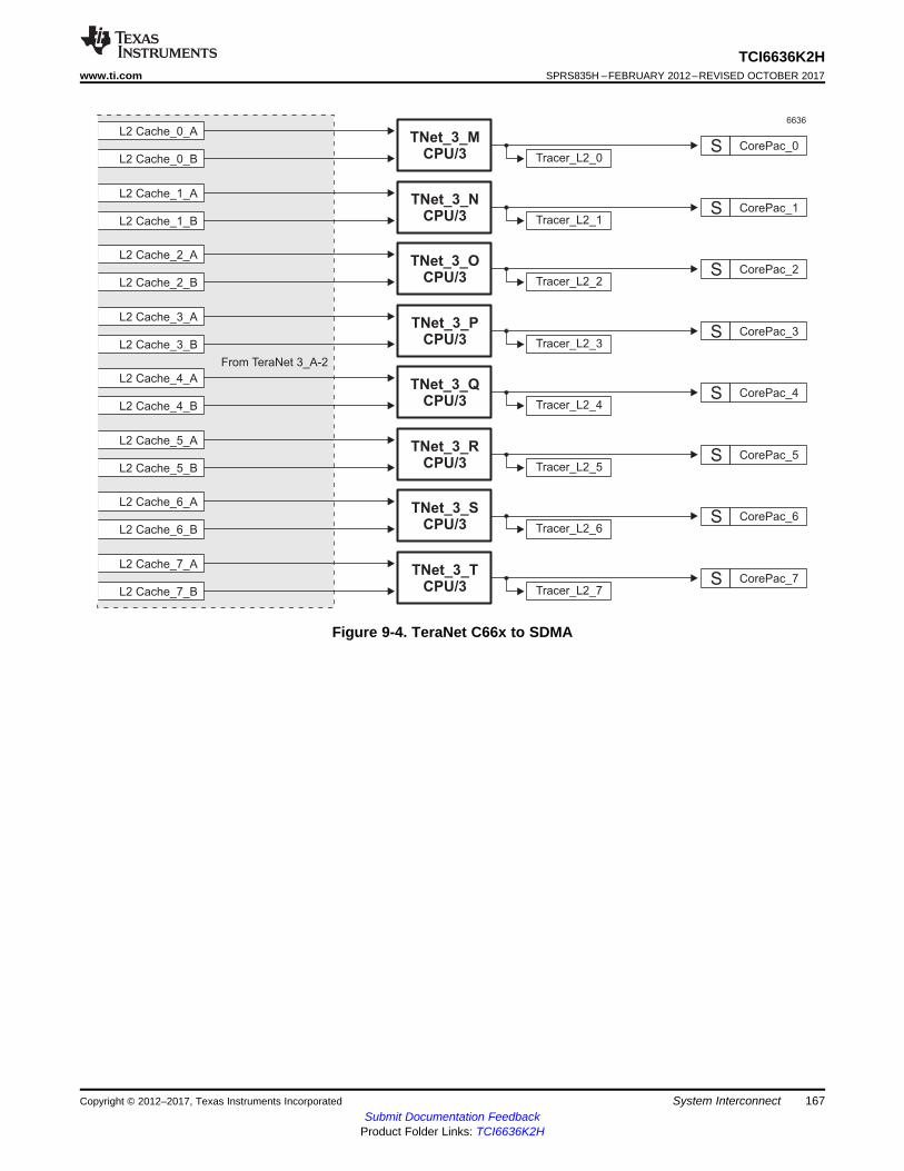
CorePac_0STracer_L2_0
TNet_3_MCPU/3
6636
CorePac_1STracer_L2_1
TNet_3_NCPU/3
CorePac_2STracer_L2_2
TNet_3_OCPU/3
CorePac_3STracer_L2_3
TNet_3_PCPU/3
CorePac_4STracer_L2_4
TNet_3_QCPU/3
CorePac_5STracer_L2_5
TNet_3_RCPU/3
CorePac_6STracer_L2_6
TNet_3_SCPU/3
CorePac_7STracer_L2_7
TNet_3_TCPU/3
L2 Cache_0_A
From TeraNet 3_A-2
L2 Cache_0_B
L2 Cache_1_A
L2 Cache_1_B
L2 Cache_2_A
L2 Cache_2_B
L2 Cache_3_A
L2 Cache_3_B
L2 Cache_4_A
L2 Cache_4_B
L2 Cache_5_A
L2 Cache_5_B
L2 Cache_6_A
L2 Cache_6_B
L2 Cache_7_A
L2 Cache_7_B
167
TCI6636K2Hwww.ti.com SPRS835H –FEBRUARY 2012–REVISED OCTOBER 2017
Submit Documentation FeedbackProduct Folder Links: TCI6636K2H
System InterconnectCopyright © 2012–2017, Texas Instruments Incorporated
Figure 9-4. TeraNet C66x to SDMA
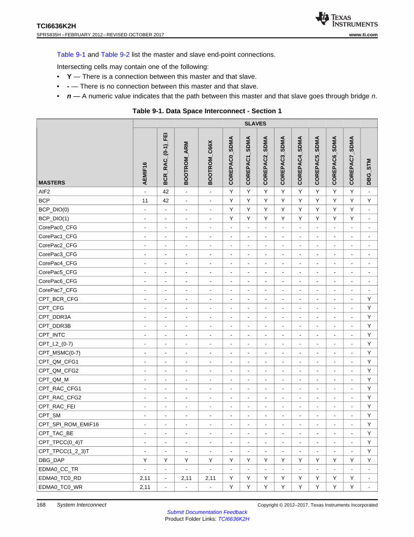
168
TCI6636K2HSPRS835H –FEBRUARY 2012–REVISED OCTOBER 2017 www.ti.com
Submit Documentation FeedbackProduct Folder Links: TCI6636K2H
System Interconnect Copyright © 2012–2017, Texas Instruments Incorporated
Table 9-1 and Table 9-2 list the master and slave end-point connections.
Intersecting cells may contain one of the following:• Y — There is a connection between this master and that slave.• - — There is no connection between this master and that slave.• n — A numeric value indicates that the path between this master and that slave goes through bridge n.
Table 9-1. Data Space Interconnect - Section 1
MASTERS
SLAVES
AEM
IF16
BC
R_R
AC
_(0-
1)_F
EI
BO
OTR
OM
_AR
M
BO
OTR
OM
_C66
X
CO
REP
AC
0_SD
MA
CO
REP
AC
1_SD
MA
CO
REP
AC
2_SD
MA
CO
REP
AC
3_SD
MA
CO
REP
AC
4_SD
MA
CO
REP
AC
5_SD
MA
CO
REP
AC
6_SD
MA
CO
REP
AC
7_SD
MA
DB
G_S
TM
AIF2 - 42 - - Y Y Y Y Y Y Y Y -BCP 11 42 - - Y Y Y Y Y Y Y Y YBCP_DIO(0) - - - - Y Y Y Y Y Y Y Y -BCP_DIO(1) - - - - Y Y Y Y Y Y Y Y -CorePac0_CFG - - - - - - - - - - - - -CorePac1_CFG - - - - - - - - - - - - -CorePac2_CFG - - - - - - - - - - - - -CorePac3_CFG - - - - - - - - - - - - -CorePac4_CFG - - - - - - - - - - - - -CorePac5_CFG - - - - - - - - - - - - -CorePac6_CFG - - - - - - - - - - - - -CorePac7_CFG - - - - - - - - - - - - -CPT_BCR_CFG - - - - - - - - - - - - YCPT_CFG - - - - - - - - - - - - YCPT_DDR3A - - - - - - - - - - - - YCPT_DDR3B - - - - - - - - - - - - YCPT_INTC - - - - - - - - - - - - YCPT_L2_(0-7) - - - - - - - - - - - - YCPT_MSMC(0-7) - - - - - - - - - - - - YCPT_QM_CFG1 - - - - - - - - - - - - YCPT_QM_CFG2 - - - - - - - - - - - - YCPT_QM_M - - - - - - - - - - - - YCPT_RAC_CFG1 - - - - - - - - - - - - YCPT_RAC_CFG2 - - - - - - - - - - - - YCPT_RAC_FEI - - - - - - - - - - - - YCPT_SM - - - - - - - - - - - - YCPT_SPI_ROM_EMIF16 - - - - - - - - - - - - YCPT_TAC_BE - - - - - - - - - - - - YCPT_TPCC(0_4)T - - - - - - - - - - - - YCPT_TPCC(1_2_3)T - - - - - - - - - - - - YDBG_DAP Y Y Y Y Y Y Y Y Y Y Y Y YEDMA0_CC_TR - - - - - - - - - - - - -EDMA0_TC0_RD 2,11 - 2,11 2,11 Y Y Y Y Y Y Y Y -EDMA0_TC0_WR 2,11 - - - Y Y Y Y Y Y Y Y -

169
TCI6636K2Hwww.ti.com SPRS835H –FEBRUARY 2012–REVISED OCTOBER 2017
Submit Documentation FeedbackProduct Folder Links: TCI6636K2H
System InterconnectCopyright © 2012–2017, Texas Instruments Incorporated
Table 9-1. Data Space Interconnect - Section 1 (continued)
MASTERS
SLAVES
AEM
IF16
BC
R_R
AC
_(0-
1)_F
EI
BO
OTR
OM
_AR
M
BO
OTR
OM
_C66
X
CO
REP
AC
0_SD
MA
CO
REP
AC
1_SD
MA
CO
REP
AC
2_SD
MA
CO
REP
AC
3_SD
MA
CO
REP
AC
4_SD
MA
CO
REP
AC
5_SD
MA
CO
REP
AC
6_SD
MA
CO
REP
AC
7_SD
MA
DB
G_S
TM
EDMA0_TC1_RD 3,11 - 3,11 3,11 Y Y Y Y Y Y Y Y -EDMA0_TC1_WR 3,11 - - - Y Y Y Y Y Y Y Y -EDMA1_CC_TR - - - - - - - - - - - - -EDMA1_TC0_RD 11 - 11 11 Y Y Y Y Y Y Y Y -EDMA1_TC0_WR 11 42 - - Y Y Y Y Y Y Y Y YEDMA1_TC1_RD 11 - Y Y Y Y Y Y Y Y Y Y -EDMA1_TC1_WR 11 42 - - Y Y Y Y Y Y Y Y -EDMA1_TC2_RD 11 - Y Y Y Y Y Y Y Y Y Y -EDMA1_TC2_WR 11 42 - - Y Y Y Y Y Y Y Y -EDMA1_TC3_RD 11 - Y Y Y Y Y Y Y Y Y Y -EDMA1_TC3_WR 11 42 - - Y Y Y Y Y Y Y Y YEDMA2_CC_TR - - - - - - - - - - - - -EDMA2_TC0_RD 11 - Y Y Y Y Y Y Y Y Y Y -EDMA2_TC0_WR 11 42 - - Y Y Y Y Y Y Y Y YEDMA2_TC1_RD 11 - Y Y Y Y Y Y Y Y Y Y -EDMA2_TC1_WR 11 42 - - Y Y Y Y Y Y Y Y -EDMA2_TC2_RD 11 - Y Y Y Y Y Y Y Y Y Y -EDMA2_TC2_WR 11 42 - - Y Y Y Y Y Y Y Y YEDMA2_TC3_RD 11 - Y Y Y Y Y Y Y Y Y Y -EDMA2_TC3_WR 11 42 - - Y Y Y Y Y Y Y Y -EDMA3_CC_TR - - - - - - - - - - - - -EDMA3_TC0_RD 11 - Y Y Y Y Y Y Y Y Y Y -EDMA3_TC0_WR 11 42 - - Y Y Y Y Y Y Y Y YEDMA3_TC1_RD 11 - Y Y Y Y Y Y Y Y Y Y -EDMA3_TC1_WR 11 42 - - Y Y Y Y Y Y Y Y -EDMA4_CC_TR - - - - - - - - - - - - -EDMA4_TC0_RD 2,11 - 2,11 2,11 Y Y Y Y Y Y Y Y -EDMA4_TC0_WR 2,11 - - - Y Y Y Y Y Y Y Y -EDMA4_TC1_RD 3,11 - 3,11 3,11 Y Y Y Y Y Y Y Y -EDMA4_TC1_WR 3,11 - - - Y Y Y Y Y Y Y Y -FFTC_0 11 42 - - Y Y Y Y Y Y Y Y YFFTC_1 11 42 - - Y Y Y Y Y Y Y Y YFFTC_2 11 42 - - Y Y Y Y Y Y Y Y YFFTC_3 11 42 - - Y Y Y Y Y Y Y Y YHyperLink0_Master 11 42 1,11 1,11 Y Y Y Y Y Y Y Y -HyperLink1_Master 11 42 1,11 1,11 Y Y Y Y Y Y Y Y -MSMC_SYS 11 42 11 11 Y Y Y Y Y Y Y Y YNETCP - - - - Y Y Y Y Y Y Y Y -PCIE 11 42 - - Y Y Y Y Y Y Y Y YQM_Master1 - - - - Y Y Y Y Y Y Y Y -QM_Master2 - - - - Y Y Y Y Y Y Y Y -

170
TCI6636K2HSPRS835H –FEBRUARY 2012–REVISED OCTOBER 2017 www.ti.com
Submit Documentation FeedbackProduct Folder Links: TCI6636K2H
System Interconnect Copyright © 2012–2017, Texas Instruments Incorporated
Table 9-1. Data Space Interconnect - Section 1 (continued)
MASTERS
SLAVES
AEM
IF16
BC
R_R
AC
_(0-
1)_F
EI
BO
OTR
OM
_AR
M
BO
OTR
OM
_C66
X
CO
REP
AC
0_SD
MA
CO
REP
AC
1_SD
MA
CO
REP
AC
2_SD
MA
CO
REP
AC
3_SD
MA
CO
REP
AC
4_SD
MA
CO
REP
AC
5_SD
MA
CO
REP
AC
6_SD
MA
CO
REP
AC
7_SD
MA
DB
G_S
TM
QM_SEC - - - - Y Y Y Y Y Y Y Y YRAC_0_BE0 - - - - Y Y Y Y Y Y Y Y -RAC_0_BE1 - - - - Y Y Y Y Y Y Y Y -RAC_1_BE0 - - - - Y Y Y Y Y Y Y Y -RAC_1_BE1 - - - - Y Y Y Y Y Y Y Y -SRIO 11 42 - - Y Y Y Y Y Y Y Y YSRIO Packet DMA 11 - - - Y Y Y Y Y Y Y Y -TAC_FEI(0-2) - - - - Y Y Y Y Y Y Y Y -USB - - - - Y Y Y Y Y Y Y Y Y
Table 9-2. Data Space Interconnect - Section 2
MASTERS
SLAVES
DD
R3B
HYP
ERLI
NK
0
HYP
ERLI
NK
1
MSM
C_S
ES
MSMC_SMS PCIE QM SPI(0-2) TAC
_BEI
TCP3
D_(
0-1)
_DA
TA
VCP2
_(0-
3)_D
ATA
AIF2 9 Y Y SES_2 SMS_2 - Y - Y - -BCP 6 Y Y SES_0 SMS_0 - Y 11 Y Y YBCP_DIO(0) 5 Y Y SES_0 SMS_0 - Y - - - -BCP_DIO(1) 9 Y Y SES_2 SMS_2 - Y - - - -CorePac0_CFG - - - - - - - - - - -CorePac1_CFG - - - - - - - - - - -CorePac2_CFG - - - - - - - - - - -CorePac3_CFG - - - - - - - - - - -CorePac4_CFG - - - - - - - - - - -CorePac5_CFG - - - - - - - - - - -CorePac6_CFG - - - - - - - - - - -CorePac7_CFG - - - - - - - - - - -CPT_BCR_CFG - - - - - - - - - - -CPT_CFG - - - - - - - - - - -CPT_DDR3A - - - - - - - - - - -CPT_DDR3B - - - - - - - - - - -CPT_INTC - - - - - - - - - - -CPT_L2_(0-7) - - - - - - - - - - -CPT_MSMC(0-7) - - - - - - - - - - -CPT_QM_CFG1 - - - - - - - - - - -CPT_QM_CFG2 - - - - - - - - - - -CPT_QM_M - - - - - - - - - - -

171
TCI6636K2Hwww.ti.com SPRS835H –FEBRUARY 2012–REVISED OCTOBER 2017
Submit Documentation FeedbackProduct Folder Links: TCI6636K2H
System InterconnectCopyright © 2012–2017, Texas Instruments Incorporated
Table 9-2. Data Space Interconnect - Section 2 (continued)
MASTERS
SLAVES
DD
R3B
HYP
ERLI
NK
0
HYP
ERLI
NK
1
MSM
C_S
ES
MSMC_SMS PCIE QM SPI(0-2) TAC
_BEI
TCP3
D_(
0-1)
_DA
TA
VCP2
_(0-
3)_D
ATA
CPT_RAC_CFG1 - - - - - - - - - - -CPT_RAC_CFG2 - - - - - - - - - - -CPT_RAC_FEI - - - - - - - - - - -CPT_SM - - - - - - - - - - -CPT_SPI_ROM_EMIF16 - - - - - - - - - - -CPT_TAC_BE - - - - - - - - - - -CPT_TPCC(0_4)T - - - - - - - - - - -CPT_TPCC(1_2_3)T - - - - - - - - - - -DBG_DAP Y Y Y Y Y Y Y Y Y Y YEDMA0_CC_TR - - - - - - - - - - -EDMA0_TC0_RD Y Y Y SES_0 SMS_0 Y Y 2,11 - - -EDMA0_TC0_WR Y Y Y SES_0 SMS_0 Y Y 2,11 - - -EDMA0_TC1_RD Y Y Y SES_1 SMS_1 Y - 3,11 - - -EDMA0_TC1_WR Y Y Y SES_1 SMS_1 Y - 3,11 - - -EDMA1_CC_TR - - - - - - - - - - -EDMA1_TC0_RD 5 Y Y SES_0 SMS_0 Y Y 11 Y Y YEDMA1_TC0_WR 5 Y Y SES_0 SMS_0 Y Y 11 Y Y YEDMA1_TC1_RD 6 Y Y SES_1 SMS_1 Y Y 11 Y Y YEDMA1_TC1_WR 6 Y Y SES_1 SMS_1 Y Y 11 Y Y YEDMA1_TC2_RD 7 Y Y SES_1 SMS_1 Y - 11 Y Y YEDMA1_TC2_WR 7 Y Y SES_1 SMS_1 Y - 11 Y Y YEDMA1_TC3_RD 8 Y Y SES_1 SMS_1 Y - 11 Y Y YEDMA1_TC3_WR 8 Y Y SES_1 SMS_1 Y - 11 Y Y YEDMA2_CC_TR - - - - - - - - - - -EDMA2_TC0_RD 9 Y Y SES_2 SMS_2 Y Y 11 Y Y YEDMA2_TC0_WR 9 Y Y SES_2 SMS_2 Y Y 11 Y Y YEDMA2_TC1_RD 10 Y Y SES_2 SMS_2 Y Y 11 Y Y YEDMA2_TC1_WR 10 Y Y SES_2 SMS_2 Y Y 11 Y Y YEDMA2_TC2_RD 5 Y Y SES_0 SMS_0 Y - 11 Y Y YEDMA2_TC2_WR 5 Y Y SES_0 SMS_0 Y - 11 Y Y YEDMA2_TC3_RD 6 Y Y SES_0 SMS_0 Y - 11 Y Y YEDMA2_TC3_WR 6 Y Y SES_0 SMS_0 Y - 11 Y Y YEDMA3_CC_TR - - - - - - - - - - -EDMA3_TC0_RD 7 Y Y SES_1 SMS_1 Y Y 11 Y Y YEDMA3_TC0_WR 7 Y Y SES_1 SMS_1 Y Y 11 Y Y YEDMA3_TC1_RD 8 Y Y SES_1 SMS_1 Y - 11 Y Y YEDMA3_TC1_WR 8 Y Y SES_1 SMS_1 Y - 11 Y Y YEDMA4_CC_TR - - - - - - - - - - -EDMA4_TC0_RD Y Y Y SES_1 SMS_1 Y Y 2,11 - - -EDMA4_TC0_WR Y Y Y SES_1 SMS_1 Y Y 2,11 - - -EDMA4_TC1_RD Y Y Y SES_1 SMS_1 Y - 3,11 - - -

172
TCI6636K2HSPRS835H –FEBRUARY 2012–REVISED OCTOBER 2017 www.ti.com
Submit Documentation FeedbackProduct Folder Links: TCI6636K2H
System Interconnect Copyright © 2012–2017, Texas Instruments Incorporated
Table 9-2. Data Space Interconnect - Section 2 (continued)
MASTERS
SLAVES
DD
R3B
HYP
ERLI
NK
0
HYP
ERLI
NK
1
MSM
C_S
ES
MSMC_SMS PCIE QM SPI(0-2) TAC
_BEI
TCP3
D_(
0-1)
_DA
TA
VCP2
_(0-
3)_D
ATA
EDMA4_TC1_WR Y Y Y SES_1 SMS_1 Y - 3,11 - - -FFTC_0 7 Y Y SES_1 SMS_1 - Y 11 11 Y YFFTC_1 8 Y Y SES_1 SMS_1 - Y 11 11 Y YFFTC_2 9 Y Y SES_2 SMS_2 - Y 11 11 Y YFFTC_3 5 Y Y SES_2 SMS_2 - Y 11 11 Y YHyperLink0_Master Y - - Y Y Y Y Y Y Y YHyperLink1_Master Y - - Y Y Y Y Y Y Y YMSMC_SYS Y Y Y - - Y Y 11 Y Y YNETCP 7 - - SES_1 SMS_1 Y Y - - - -PCIE 10 10 10 SES_2 SMS_2 - Y 11 Y Y YQM_Master1 5 Y Y SES_0 SMS_0 - Y - - Y -QM_Master2 8 Y Y SES_1 SMS_1 - Y - - Y -QM_SEC Y Y Y SES_2 SMS_2 - - - - - -RAC_0_BE0 Y Y Y - - - - - - - -RAC_0_BE1 Y Y Y SES_2 SMS_2 - 3 - - - -RAC_1_BE0 Y Y Y SES_0 SMS_0 - - - - - -RAC_1_BE1 Y Y Y SES_2 SMS_2 - 3 - - - -SRIO 9 Y Y SES_2 SMS_2 - Y 11 Y Y YSRIO Packet DMA 9 - - SES_2 SMS_2 - Y - - - -TAC_FEI(0-2) 10 Y Y SES_2 SMS_2 - - - - - -USB 5 Y Y SES_0 SMS_0 - Y - - - -

Tera
Net
3P
_A
CP
U/3
To TeraNet_3P_Tracer
Bridge_12
Bridge_13
Bridge_14
From TeraNet_3_A
CorePac_0 M
MCorePac_1
CorePac_2 M
MCorePac_3
TBR_SYS_ARM_CorePac
SemaphoreSTracer_SM
MPU_10
Tracer_QM_CFG2MPU_6
CP_INTC0-2S
ARM INTCSTNet_3P_L
CPU/3MPU_9
Tracer_INTC
MPU ( 15)´S
To TeraNet_3P_B
6636
CorePac_4 M
MCorePac_5
CorePac_6 M
MCorePac_7
SCC3S
TNet_3P_CCPU/3
Tracer_EDMA
CC1 - CC3
Tracer_CFGMPU_0
TC ( 2)´
SCC2S
TC ( 4)´
SCC1S
TC ( 4)´
TNet_3P_MCPU/3
Tracer_EDMA
CC0 & CC4
S
CC4STC ( 2)´
S
CC0STC ( 2)´
QM_SS_CFG2M
Tracer_QM_CFG1MPU_2 QM_SS_
CFG1M
Tracer_BCR_CFGMPU_3 BCR CFGS
DBG_TBR_SYS(Debug_SS)
TETB
CorePac ( 8)´
RAC_1_CFGS
RAC_0_CFGSTNet_3P_H
CPU/3MPU_4
Tracer_RAC_CFG_1
From TeraNet_3_C
173
TCI6636K2Hwww.ti.com SPRS835H –FEBRUARY 2012–REVISED OCTOBER 2017
Submit Documentation FeedbackProduct Folder Links: TCI6636K2H
System InterconnectCopyright © 2012–2017, Texas Instruments Incorporated
9.3 TeraNet Switch Fabric Connections Matrix - Configuration SpaceFigure 9-5, Figure 9-6, Figure 9-7, and Figure 9-8 show the connections between masters and slavesthrough various sections of the TeraNet.
Figure 9-5. TeraNet 3P_A

Tera
Net
3P
_B
C
PU
/3
From TeraNet_3P_A
6636
CP_T0-T8(MSMC)S
VCP2_3S
VCP2_2S
VCP2_1S
VCP2_0S
TNet_3P_ECPU/3
S
TCP3d_0STNet_3P_F
CPU/3TCP3d_1
S
S
S
FFTC_0S
TNet_3P_GCPU/3
FFTC_1
FFTC_2
FFTC_3
CP_T ( 23)´STNet_3P_DCPU/3
SRIOS
TACS
BCP CFGS
NetCPS
AIF2S
TNet_3P_NCPU/3
Bridge 20MPU_11To TeraNet_6P_B
174
TCI6636K2HSPRS835H –FEBRUARY 2012–REVISED OCTOBER 2017 www.ti.com
Submit Documentation FeedbackProduct Folder Links: TCI6636K2H
System Interconnect Copyright © 2012–2017, Texas Instruments Incorporated
Figure 9-6. TeraNet 3P_B

Tera
Net
6P
_B
C
PU
/6
6636
S
S
S
UART ( 2)´S
I C ( 3)2
´
GPIO
AIF2 B4 SerDes CFG
Timer ( 20)´S
USIMS
S
Debug SSS
PLL_CTLS
GPSCS
BOOT_CFGS
Bridge 20
From TeraNet_3P_B
OTP
S AIF2 B8 SerDes CFG
S USB PHY CFG
S PCIe SerDes CFG
S HyperLink SerDes CFG
S SRIO SerDes CFG
S NetCP SerDes CFG
S DDR3B PHY CFG
S
S
DDR3A PHY CFG
USB MMR CFG
S
S SmartReflex1
SmartReflex0
175
TCI6636K2Hwww.ti.com SPRS835H –FEBRUARY 2012–REVISED OCTOBER 2017
Submit Documentation FeedbackProduct Folder Links: TCI6636K2H
System InterconnectCopyright © 2012–2017, Texas Instruments Incorporated
Figure 9-7. TeraNet 6P_B
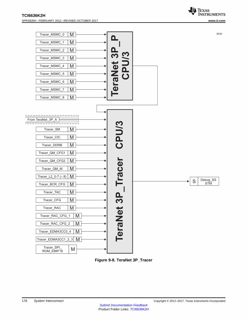
Tera
Net
3P
_T
racer
C
PU
/3
Debug_SSSTMS
From TeraNet_3P_A
6636
Tracer_EDMA3CC1_2_3 M
M
Tracer_SPI_ROM_EMIF16 M
Tracer_EDMA3CC0_4
MTracer_CFG
Tracer_TAC M
MTracer_RAC
MTracer_RAC_CFG_2
Tracer_RAC_CFG_1 M
MTracer_BCR_CFG
MTracer_L2_0-7 ( 8)´
Tracer_QM_M M
MTracer_QM_CFG2
MTracer_QM_CFG1
Tracer_DDRB M
MTracer_CIC
MTracer_SM
Tera
Net
3P
_P
CP
U/3
MTracer_MSMC_7
MTracer_MSMC_6
MTracer_MSMC_5
MTracer_MSMC_4
MTracer_MSMC_3
MTracer_MSMC_2
MTracer_MSMC_1
MTracer_MSMC_0
MTracer_MSMC_8
176
TCI6636K2HSPRS835H –FEBRUARY 2012–REVISED OCTOBER 2017 www.ti.com
Submit Documentation FeedbackProduct Folder Links: TCI6636K2H
System Interconnect Copyright © 2012–2017, Texas Instruments Incorporated
Figure 9-8. TeraNet 3P_Tracer

177
TCI6636K2Hwww.ti.com SPRS835H –FEBRUARY 2012–REVISED OCTOBER 2017
Submit Documentation FeedbackProduct Folder Links: TCI6636K2H
System InterconnectCopyright © 2012–2017, Texas Instruments Incorporated
Table 9-3, Table 9-4, and Table 9-5 list the master and slave end-point connections.
Intersecting cells may contain one of the following:• Y — There is a connection between this master and that slave.• - — There is no connection between this master and that slave.• n — A numeric value indicates that the path between this master and that slave goes through bridge n.
Table 9-3. Configuration Space Interconnect - Section 1
MASTERS
SLAVES
AD
TF(0
-7)_
CFG
AIF
2_C
FG
AIF
2_SE
RD
ES_B
4_C
FG
AIF
2_SE
RD
ES_B
8_C
FG
AR
M_C
FG
BC
P_C
FG
BC
R_C
FG
BO
OTC
FG_C
FG
CP_
INTC
_CFG
CPT
_BC
R_C
FG_C
FG
CPT
_CFG
_CFG
CPT
_DD
R3A
_CFG
CPT
_DD
R3B
_CFG
CPT
_IN
TC(0
-2)_
CFG
CPT
_L2_
(0-7
)_C
FG
CPT
_MSM
C(0
-7)_
CFG
CPT
_QM
_CFG
1_C
FG
CPT
_QM
_CFG
2_C
FG
CPT
_QM
_M_C
FG
CPT
_RA
C_C
FG1_
CFG
CPT
_RA
C_C
FG2_
CFG
CPT
_RA
C_F
EI_C
FG
CPT
_SM
_CFG
CPT
_SPI
_RO
M_E
MIF
16_C
FG
CPT
_TA
C_B
E_C
FG
CPT
_TPC
C0_
4_C
FG
CPT
_TPC
C1_
2_3_
CFG
AIF2 - - - - - - - - - - - - - - - - - - - - - - - - - - -
BCP Packet DMA 12 12 12 12 12 - 12 12 12 12 12 12 12 12 12 12 12 12 12 12 12 12 12 12 12 12 12
BCP_DIO(0-1) - - - - - - - - - - - - - - - - - - - - - - - - - - -
CorePac0_CFG Y Y Y Y Y Y Y Y Y Y Y Y Y Y Y Y Y Y Y Y Y Y Y Y Y Y Y
CorePac1_CFG Y Y Y Y Y Y Y Y Y Y Y Y Y Y Y Y Y Y Y Y Y Y Y Y Y Y Y
CorePac2_CFG Y Y Y Y Y Y Y Y Y Y Y Y Y Y Y Y Y Y Y Y Y Y Y Y Y Y Y
CorePac3_CFG Y Y Y Y Y Y Y Y Y Y Y Y Y Y Y Y Y Y Y Y Y Y Y Y Y Y Y
CorePac4_CFG Y Y Y Y Y Y Y Y Y Y Y Y Y Y Y Y Y Y Y Y Y Y Y Y Y Y Y
CorePac5_CFG Y Y Y Y Y Y Y Y Y Y Y Y Y Y Y Y Y Y Y Y Y Y Y Y Y Y Y
CorePac6_CFG Y Y Y Y Y Y Y Y Y Y Y Y Y Y Y Y Y Y Y Y Y Y Y Y Y Y Y
CorePac7_CFG Y Y Y Y Y Y Y Y Y Y Y Y Y Y Y Y Y Y Y Y Y Y Y Y Y Y Y
DBG_DAP Y Y Y Y Y Y Y Y Y Y Y Y Y Y Y Y Y Y Y Y Y Y Y Y Y Y Y
EDMA0_CC_TR - - - - - - - - - - - - - - - - - - - - - - - - - - -
EDMA0_TC0_RD - - - - - - - - - - - - - - - - - - - - - - - - - - -
EDMA0_TC0_WR - - - - - - - - - - - - - - - - - - - - - - - - - - -
EDMA0_TC1_RD - - - - - - - - - - - - - - - - - - - - - - - - - - -
EDMA0_TC1_WR - - - - - - - - - - - - - - - - - - - - - - - - - - -
EDMA1_CC_TR - - - - - - - - - - - - - - - - - - - - - - - - - - -
EDMA1_TC0_RD 12 12 12 12 12 12 12 12 12 12 12 12 12 12 12 12 12 12 12 12 12 12 12 12 12 12 12
EDMA1_TC0_WR 12 12 12 12 12 12 12 12 12 12 12 12 12 12 12 12 12 12 12 12 12 12 12 12 12 12 12
EDMA1_TC1_RD - - - - - - - - - - - - - - - - - - - - - - - - - - -
EDMA1_TC1_WR - - - - - - - - - - - - - - - - - - - - - - - - - - -
EDMA1_TC2_RD - - - - - - - - - - - - - - - - - - - - - - - - - - -
EDMA1_TC2_WR - - - - - - - - - - - - - - - - - - - - - - - - - - -
EDMA1_TC3_RD 12 12 12 12 12 12 12 12 12 12 12 12 12 12 12 12 12 12 12 12 12 12 12 12 12 12 12
EDMA1_TC3_WR 12 12 12 12 12 12 12 12 12 12 12 12 12 12 12 12 12 12 12 12 12 12 12 12 12 12 12
EDMA2_CC_TR - - - - - - - - - - - - - - - - - - - - - - - - - - -
EDMA2_TC0_RD 12 12 12 12 12 12 12 12 12 12 12 12 12 12 12 12 12 12 12 12 12 12 12 12 12 12 12
EDMA2_TC0_WR 12 12 12 12 12 12 12 12 12 12 12 12 12 12 12 12 12 12 12 12 12 12 12 12 12 12 12
EDMA2_TC1_RD - - - - - - - - - - - - - - - - - - - - - - - - - - -
EDMA2_TC1_WR - - - - - - - - - - - - - - - - - - - - - - - - - - -
EDMA2_TC2_RD 12 12 12 12 12 12 12 12 12 12 12 12 12 12 12 12 12 12 12 12 12 12 12 12 12 12 12
EDMA2_TC2_WR 12 12 12 12 12 12 12 12 12 12 12 12 12 12 12 12 12 12 12 12 12 12 12 12 12 12 12
EDMA2_TC3_RD - - - - - - - - - - - - - - - - - - - - - - - - - - -
EDMA2_TC3_WR - - - - - - - - - - - - - - - - - - - - - - - - - - -
EDMA3_CC_TR - - - - - - - - - - - - - - - - - - - - - - - - - - -
EDMA3_TC0_RD 13 13 13 13 13 13 13 13 13 13 13 13 13 13 13 13 13 13 13 13 13 13 13 13 13 13 13
EDMA3_TC0_WR 13 13 13 13 13 13 13 13 13 13 13 13 13 13 13 13 13 13 13 13 13 13 13 13 13 13 13
EDMA3_TC1_RD - - - - - - - - - - - - - - - - - - - - - - - - - - -
EDMA3_TC1_WR - - - - - - - - - - - - - - - - - - - - - - - - - - -

178
TCI6636K2HSPRS835H –FEBRUARY 2012–REVISED OCTOBER 2017 www.ti.com
Submit Documentation FeedbackProduct Folder Links: TCI6636K2H
System Interconnect Copyright © 2012–2017, Texas Instruments Incorporated
Table 9-3. Configuration Space Interconnect - Section 1 (continued)
MASTERS
SLAVES
AD
TF(0
-7)_
CFG
AIF
2_C
FG
AIF
2_SE
RD
ES_B
4_C
FG
AIF
2_SE
RD
ES_B
8_C
FG
AR
M_C
FG
BC
P_C
FG
BC
R_C
FG
BO
OTC
FG_C
FG
CP_
INTC
_CFG
CPT
_BC
R_C
FG_C
FG
CPT
_CFG
_CFG
CPT
_DD
R3A
_CFG
CPT
_DD
R3B
_CFG
CPT
_IN
TC(0
-2)_
CFG
CPT
_L2_
(0-7
)_C
FG
CPT
_MSM
C(0
-7)_
CFG
CPT
_QM
_CFG
1_C
FG
CPT
_QM
_CFG
2_C
FG
CPT
_QM
_M_C
FG
CPT
_RA
C_C
FG1_
CFG
CPT
_RA
C_C
FG2_
CFG
CPT
_RA
C_F
EI_C
FG
CPT
_SM
_CFG
CPT
_SPI
_RO
M_E
MIF
16_C
FG
CPT
_TA
C_B
E_C
FG
CPT
_TPC
C0_
4_C
FG
CPT
_TPC
C1_
2_3_
CFG
EDMA4_CC_TR - - - - - - - - - - - - - - - - - - - - - - - - - - -
EDMA4_TC0_RD - - - - - - - - - - - - - - - - - - - - - - - - - - -
EDMA4_TC0_WR - - - - - - - - - - - - - - - - - - - - - - - - - - -
EDMA4_TC1_RD - - - - - - - - - - - - - - - - - - - - - - - - - - -
EDMA4_TC1_WR - - - - - - - - - - - - - - - - - - - - - - - - - - -
FFTC_0 12 12 12 12 12 12 12 12 12 12 12 12 12 12 12 12 12 12 12 12 12 12 12 12 12 12 12
FFTC_1 12 12 12 12 12 12 12 12 12 12 12 12 12 12 12 12 12 12 12 12 12 12 12 12 12 12 12
FFTC_2 12 12 12 12 12 12 12 12 12 12 12 12 12 12 12 12 12 12 12 12 12 12 12 12 12 12 12
FFTC_3 12 12 12 12 12 12 12 12 12 12 12 12 12 12 12 12 12 12 12 12 12 12 12 12 12 12 12
HyperLink0_Master 12 12 12 12 12 12 12 12 12 12 12 12 12 12 12 12 12 12 12 12 12 12 12 12 12 12 12
HyperLink1_Master 12 12 12 12 12 12 12 12 12 12 12 12 12 12 12 12 12 12 12 12 12 12 12 12 12 12 12
MSMC_SYS Y Y Y Y Y Y Y Y Y Y Y Y Y Y Y Y Y Y Y Y Y Y Y Y Y Y Y
NETCP - - - - - - - - - - - - - - - - - - - - - - - - - - -
PCIE 12 12 12 12 12 12 12 12 12 12 12 12 12 12 12 12 12 12 12 12 12 12 12 12 12 12 12
QM_Master1 - - - - - - - - - - - - - - - - - - - - - - - - - - -
QM_Master2 - - - - - - - - - - - - - - - - - - - - - - - - - - -
QM_SEC - - - - 12 - - - - - - - - - - - - - - - - - - - - - -
RAC_(0-1)_BE0 - - - - - - - - - - - - - - - - - - - - - - - - - - -
RAC_(0-1)_BE1 - - - - - - - - - - - - - - - - - - - - - - - - - - -
SRIO 14 14 14 14 14 14 14 14 14 14 14 14 14 14 14 14 14 14 14 14 14 14 14 14 14 14 14
SRIO Packet DMA - - - - - - - - - - - - - - - - - - - - - - - - - - -
TAC_FEI_(0-2) - - - - - - - - - - - - - - - - - - - - - - - - - - -
USB - - - - - - - - - - - - - - - - - - - - - - - - - - -
Table 9-4. Configuration Space Interconnect - Section 2
MASTERS
SLAVES
DB
G_C
FG
DB
G_T
BR
_SYS
DD
R3A
_PH
Y_C
FG
DD
R3B
_PH
Y_C
FG
EDM
A0_
CC
_CFG
EDM
A0_
TC(0
-1)_
CFG
EDM
A1_
CC
_CFG
EDM
A1_
TC(0
-3)_
CFG
EDM
A2_
CC
_CFG
EDM
A2_
TC(0
-3)_
CFG
EDM
A3_
CC
_CFG
EDM
A3_
TC(0
-1)_
CFG
EDM
A4_
CC
_CFG
EDM
A4_
TC(0
-1)_
CFG
FFTC
_(0-
3)_C
FG
GIC
_CFG
GPI
O_C
FG
HYP
ERLI
NK
0_SE
RD
ES_C
FG
HYP
ERLI
NK
1_SE
RD
ES_C
FG
I2C
(0-2
)_C
FG
MPU
(0-1
4)_C
FG
NET
CP_
CFG
NET
CP_
SER
DES
_CFG
OTP
_CFG
PCIE
_SER
DES
_CFG
PLL_
CTL
_CFG
PSC
_CFG
QM
_CFG
1
AIF2 - - - - - - - - - - - - - - - - - - - - - - - - - - - -
BCP Packet DMA 12 12 12 12 12 12 12 12 12 12 12 12 12 12 12 - 12 12 12 12 12 12 12 12 12 12 12 12
BCP_DIO(0-1) - - - - - - - - - - - - - - - - - - - - - - - - - - - -
CorePac0_CFG Y Y Y Y Y Y Y Y Y Y Y Y Y Y Y - Y Y Y Y Y Y Y Y Y Y Y Y
CorePac1_CFG Y Y Y Y Y Y Y Y Y Y Y Y Y Y Y - Y Y Y Y Y Y Y Y Y Y Y Y
CorePac2_CFG Y Y Y Y Y Y Y Y Y Y Y Y Y Y Y - Y Y Y Y Y Y Y Y Y Y Y Y
CorePac3_CFG Y Y Y Y Y Y Y Y Y Y Y Y Y Y Y - Y Y Y Y Y Y Y Y Y Y Y Y
CorePac4_CFG Y Y Y Y Y Y Y Y Y Y Y Y Y Y Y - Y Y Y Y Y Y Y Y Y Y Y Y
CorePac5_CFG Y Y Y Y Y Y Y Y Y Y Y Y Y Y Y - Y Y Y Y Y Y Y Y Y Y Y Y
CorePac6_CFG Y Y Y Y Y Y Y Y Y Y Y Y Y Y Y - Y Y Y Y Y Y Y Y Y Y Y Y
CorePac7_CFG Y Y Y Y Y Y Y Y Y Y Y Y Y Y Y - Y Y Y Y Y Y Y Y Y Y Y Y
DBG_DAP Y Y Y Y Y Y Y Y Y Y Y Y Y Y Y Y Y Y Y Y Y Y Y Y Y Y Y Y
EDMA0_CC_TR - - - - - Y - - - - - - - - - - - - - - - - - - - - - -
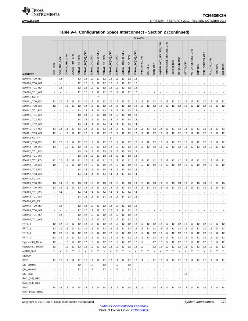
179
TCI6636K2Hwww.ti.com SPRS835H –FEBRUARY 2012–REVISED OCTOBER 2017
Submit Documentation FeedbackProduct Folder Links: TCI6636K2H
System InterconnectCopyright © 2012–2017, Texas Instruments Incorporated
Table 9-4. Configuration Space Interconnect - Section 2 (continued)
MASTERS
SLAVES
DB
G_C
FG
DB
G_T
BR
_SYS
DD
R3A
_PH
Y_C
FG
DD
R3B
_PH
Y_C
FG
EDM
A0_
CC
_CFG
EDM
A0_
TC(0
-1)_
CFG
EDM
A1_
CC
_CFG
EDM
A1_
TC(0
-3)_
CFG
EDM
A2_
CC
_CFG
EDM
A2_
TC(0
-3)_
CFG
EDM
A3_
CC
_CFG
EDM
A3_
TC(0
-1)_
CFG
EDM
A4_
CC
_CFG
EDM
A4_
TC(0
-1)_
CFG
FFTC
_(0-
3)_C
FG
GIC
_CFG
GPI
O_C
FG
HYP
ERLI
NK
0_SE
RD
ES_C
FG
HYP
ERLI
NK
1_SE
RD
ES_C
FG
I2C
(0-2
)_C
FG
MPU
(0-1
4)_C
FG
NET
CP_
CFG
NET
CP_
SER
DES
_CFG
OTP
_CFG
PCIE
_SER
DES
_CFG
PLL_
CTL
_CFG
PSC
_CFG
QM
_CFG
1
EDMA0_TC0_RD - 12 - - 12 12 12 12 12 12 12 12 12 12 - - - - - - - - - - - - - -
EDMA0_TC0_WR - - - - 12 12 12 12 12 12 12 12 12 12 - - - - - - - - - - - - - -
EDMA0_TC1_RD - 12 - - 12 12 12 12 12 12 12 12 12 12 - - - - - - - - - - - - - -
EDMA0_TC1_WR - - - - 12 12 12 12 12 12 12 12 12 12 - - - - - - - - - - - - - -
EDMA1_CC_TR - - - - - - - Y - - - - - - - - - - - - - - - - - - - -
EDMA1_TC0_RD 12 12 12 12 12 12 12 12 12 12 12 12 12 12 12 12 12 12 12 12 12 12 12 12 12 12 12 12
EDMA1_TC0_WR 12 - 12 12 12 12 12 12 12 12 12 12 12 12 12 12 12 12 12 12 12 12 12 12 12 12 12 12
EDMA1_TC1_RD - - - - 13 13 13 13 13 13 13 13 13 13 - - - - - - - - - - - - - -
EDMA1_TC1_WR - - - - 13 13 13 13 13 13 13 13 13 13 - - - - - - - - - - - - - -
EDMA1_TC2_RD - - - - 14 14 14 14 14 14 14 14 14 14 - - - - - - - - - - - - - -
EDMA1_TC2_WR - - - - 14 14 14 14 14 14 14 14 14 14 - - - - - - - - - - - - - -
EDMA1_TC3_RD 12 12 12 12 12 12 12 12 12 12 12 12 12 12 12 12 12 12 12 12 12 12 12 12 12 12 12 12
EDMA1_TC3_WR 12 - 12 12 12 12 12 12 12 12 12 12 12 12 12 12 12 12 12 12 12 12 12 12 12 12 12 12
EDMA2_CC_TR - - - - - - - - - Y - - - - - - - - - - - - - - - - - -
EDMA2_TC0_RD 12 12 12 12 12 12 12 12 12 12 12 12 12 12 12 12 12 12 12 12 12 12 12 12 12 12 12 12
EDMA2_TC0_WR 12 - 12 12 12 12 12 12 12 12 12 12 12 12 12 12 12 12 12 12 12 12 12 12 12 12 12 12
EDMA2_TC1_RD - - - - 13 13 13 13 13 13 13 13 13 13 - - - - - - - - - - - - - -
EDMA2_TC1_WR - - - - 13 13 13 13 13 13 13 13 13 13 - - - - - - - - - - - - - -
EDMA2_TC2_RD 12 12 12 12 12 12 12 12 12 12 12 12 12 12 12 12 12 12 12 12 12 12 12 12 12 12 12 12
EDMA2_TC2_WR 12 - 12 12 12 12 12 12 12 12 12 12 12 12 12 12 12 12 12 12 12 12 12 12 12 12 12 12
EDMA2_TC3_RD - - - - 14 14 14 14 14 14 14 14 14 14 - - - - - - - - - - - - - -
EDMA2_TC3_WR - - - - 14 14 14 14 14 14 14 14 14 14 - - - - - - - - - - - - - -
EDMA3_CC_TR - - - - - - - - - - - - - - - - - - - - - - - - - - - -
EDMA3_TC0_RD 13 13 13 13 13 13 13 13 13 13 13 13 13 13 13 13 13 13 13 13 13 13 13 13 13 13 13 13
EDMA3_TC0_WR 13 13 13 13 13 13 13 13 13 13 13 13 13 13 13 13 13 13 13 13 13 13 13 13 13 13 13 13
EDMA3_TC1_RD - 14 - - 14 14 14 14 14 14 14 14 14 14 - - - - - - - - - - - - - -
EDMA3_TC1_WR - - - - 14 14 14 14 14 14 14 14 14 14 - - - - - - - - - - - - - -
EDMA4_CC_TR - - - - - - - - - - - - - - - - - - - - - - - - - - - -
EDMA4_TC0_RD - 12 - - 12 12 12 12 12 12 12 12 12 12 - - - - - - - - - - - - - -
EDMA4_TC0_WR - - - - 12 12 12 12 12 12 12 12 12 12 - - - - - - - - - - - - - -
EDMA4_TC1_RD - 12 - - 12 12 12 12 12 12 12 12 12 12 - - - - - - - - - - - - - -
EDMA4_TC1_WR - - - - 12 12 12 12 12 12 12 12 12 12 - - - - - - - - - - - - - -
FFTC_0 12 12 12 12 12 12 12 12 12 12 12 12 12 12 12 12 12 12 12 12 12 12 12 12 12 12 12 12
FFTC_1 12 12 12 12 12 12 12 12 12 12 12 12 12 12 12 12 12 12 12 12 12 12 12 12 12 12 12 12
FFTC_2 12 12 12 12 12 12 12 12 12 12 12 12 12 12 12 12 12 12 12 12 12 12 12 12 12 12 12 12
FFTC_3 12 12 12 12 12 12 12 12 12 12 12 12 12 12 12 12 12 12 12 12 12 12 12 12 12 12 12 12
HyperLink0_Master 12 - 12 12 12 12 12 12 12 12 12 12 12 12 12 - 12 12 12 12 12 12 12 12 12 12 12 12
HyperLink1_Master 12 - 12 12 12 12 12 12 12 12 12 12 12 12 12 - 12 12 12 12 12 12 12 12 12 12 12 12
MSMC_SYS Y Y Y Y Y Y Y Y Y Y Y Y Y Y Y Y Y Y Y Y Y Y Y Y Y Y Y Y
NETCP - - - - - - - - - - - - - - - - - - - - - - - - - - - -
PCIE 12 12 12 12 12 12 12 12 12 12 12 12 12 12 12 - 12 12 12 12 12 12 12 12 12 12 12 12
QM_Master1 - - - - 12 - 12 - 12 - 12 - 12 - - - - - - - - - - - - - - -
QM_Master2 - - - - 12 - 12 - 12 - 12 - 12 - - - - - - - - - - - - - - -
QM_SEC - - - - - - - - - - - - - - - - - - - - - 12 - - - - - -
RAC_(0-1)_BE0 - - - - - - - - - - - - - - - - - - - - - - - - - - - -
RAC_(0-1)_BE1 - - - - - - - - - - - - - - - - - - - - - - - - - - - -
SRIO 14 14 14 14 14 14 14 14 14 14 14 14 14 14 14 - 14 14 14 14 14 14 14 14 14 14 14 14
SRIO Packet DMA - - - - - - - - - - - - - - - - - - - - - - - - - - - -

180
TCI6636K2HSPRS835H –FEBRUARY 2012–REVISED OCTOBER 2017 www.ti.com
Submit Documentation FeedbackProduct Folder Links: TCI6636K2H
System Interconnect Copyright © 2012–2017, Texas Instruments Incorporated
Table 9-4. Configuration Space Interconnect - Section 2 (continued)
MASTERS
SLAVES
DB
G_C
FG
DB
G_T
BR
_SYS
DD
R3A
_PH
Y_C
FG
DD
R3B
_PH
Y_C
FG
EDM
A0_
CC
_CFG
EDM
A0_
TC(0
-1)_
CFG
EDM
A1_
CC
_CFG
EDM
A1_
TC(0
-3)_
CFG
EDM
A2_
CC
_CFG
EDM
A2_
TC(0
-3)_
CFG
EDM
A3_
CC
_CFG
EDM
A3_
TC(0
-1)_
CFG
EDM
A4_
CC
_CFG
EDM
A4_
TC(0
-1)_
CFG
FFTC
_(0-
3)_C
FG
GIC
_CFG
GPI
O_C
FG
HYP
ERLI
NK
0_SE
RD
ES_C
FG
HYP
ERLI
NK
1_SE
RD
ES_C
FG
I2C
(0-2
)_C
FG
MPU
(0-1
4)_C
FG
NET
CP_
CFG
NET
CP_
SER
DES
_CFG
OTP
_CFG
PCIE
_SER
DES
_CFG
PLL_
CTL
_CFG
PSC
_CFG
QM
_CFG
1
TAC_FEI_(0-2) - - - - - - - - - - - - - - - - - - - - - - - - - - - -
USB - 12 - - - - - - - - - - - - - - - - - - - - - - - - - -
Table 9-5. Configuration Space Interconnect - Section 3
MASTERS
SLAVES
QM
_CFG
2
RA
C_(
0-1)
_CFG
SEC
_MG
R_C
FG
SM_C
FG
SR_C
FG(0
-1)
SRIO
_CFG
SRIO
_SER
DES
_CFG
TAC
_CFG
TBR
_SYS
_AR
M
TCP3
D_(
0-1)
_CFG
TETB
0_C
FG
TETB
1_C
FG
TETB
2_C
FG
TETB
3_C
FG
TETB
4_C
FG
TETB
5_C
FG
TETB
6_C
FG
TETB
7_C
FG
TIM
ER(0
-19)
_CFG
UA
RT(
0-1)
_CFG
USB
_MM
R_C
FG
USB
_PH
Y_C
FG
USI
M_C
FG
VCP2
_(0-
3)_C
FG
AIF2 - - - - - - - - - - - - - - - - - - - - - - - -
BCP Packet DMA 12 12 12 12 12 12 12 12 12 12 12 12 12 12 12 12 12 12 12 12 12 12 12 12
BCP_DIO(0-1) - - - - - - - - - - - - - - - - - - - - - - - -
CorePac0_CFG Y Y Y Y Y Y Y Y Y Y Y Y Y Y Y Y Y Y Y Y Y Y Y Y
CorePac1_CFG Y Y Y Y Y Y Y Y Y Y Y Y Y Y Y Y Y Y Y Y Y Y Y Y
CorePac2_CFG Y Y Y Y Y Y Y Y Y Y Y Y Y Y Y Y Y Y Y Y Y Y Y Y
CorePac3_CFG Y Y Y Y Y Y Y Y Y Y Y Y Y Y Y Y Y Y Y Y Y Y Y Y
CorePac4_CFG Y Y Y Y Y Y Y Y Y Y Y Y Y Y Y Y Y Y Y Y Y Y Y Y
CorePac5_CFG Y Y Y Y Y Y Y Y Y Y Y Y Y Y Y Y Y Y Y Y Y Y Y Y
CorePac6_CFG Y Y Y Y Y Y Y Y Y Y Y Y Y Y Y Y Y Y Y Y Y Y Y Y
CorePac7_CFG Y Y Y Y Y Y Y Y Y Y Y Y Y Y Y Y Y Y Y Y Y Y Y Y
DBG_DAP Y Y Y Y Y Y Y Y Y Y Y Y Y Y Y Y Y Y Y Y Y Y Y Y
EDMA0_CC_TR - - - - - - - - - - - - - - - - - - - - - - - -
EDMA0_TC0_RD - - - - - - - - - - - - - - 12 12 - - - - - - - -
EDMA0_TC0_WR - - - - - - - - - - - - - - - - - - - - - - - -
EDMA0_TC1_RD - - - - - - - - - - - - - - 12 12 - - - - - - - -
EDMA0_TC1_WR - - - - - - - - - - - - - - - - - - - - - - - -
EDMA1_CC_TR - - - - - - - - - - - - - - - - - - - - - - - -
EDMA1_TC0_RD 12 12 12 - 12 12 12 12 12 12 - - - - 12 12 - - 12 12 12 12 12 12
EDMA1_TC0_WR 12 12 12 - 12 12 12 12 12 12 - - - - - - - - 12 12 12 12 12 12
EDMA1_TC1_RD - - - - - - - - - - 13 13 - - - - 13 - - - - - - -
EDMA1_TC1_WR - - - - - - - - - - - - - - - - - - - - - - - -
EDMA1_TC2_RD - - - - - - - - - - - - 14 14 - - - 14 - - - - - -
EDMA1_TC2_WR - - - - - - - - - - - - - - - - - - - - - - - -
EDMA1_TC3_RD 12 12 12 - 12 12 12 12 12 12 - - - - 12 12 - - 12 12 12 12 12 12
EDMA1_TC3_WR 12 12 12 - 12 12 12 12 12 12 - - - - - - - - 12 12 12 12 12 12
EDMA2_CC_TR - - - - - - - - - - - - - - - - - - - - - - - -
EDMA2_TC0_RD 12 12 12 - 12 12 12 12 12 12 - - - - Y Y - - 12 12 12 12 12 12
EDMA2_TC0_WR 12 12 12 - 12 12 12 12 12 12 - - - - - - - - 12 12 12 12 12 12
EDMA2_TC1_RD - - - - - - - - - - 13 13 - - - - 13 - - - - - - -
EDMA2_TC1_WR - - - - - - - - - - - - - - - - - - - - - - - -
EDMA2_TC2_RD 12 12 12 - 12 12 12 12 12 12 - - - - 12 12 - - 12 12 12 12 12 12
EDMA2_TC2_WR 12 12 12 - 12 12 12 12 12 12 - - - - - - - - 12 12 12 12 12 12
EDMA2_TC3_RD - - - - - - - - - - - - 14 14 - - - 14 - - - - - -
EDMA2_TC3_WR - - - - - - - - - - - - - - - - - - - - - - - -
EDMA3_CC_TR - - - - - - - - - - - - - - - - - - - - - - - -

181
TCI6636K2Hwww.ti.com SPRS835H –FEBRUARY 2012–REVISED OCTOBER 2017
Submit Documentation FeedbackProduct Folder Links: TCI6636K2H
System InterconnectCopyright © 2012–2017, Texas Instruments Incorporated
Table 9-5. Configuration Space Interconnect - Section 3 (continued)
MASTERS
SLAVES
QM
_CFG
2
RA
C_(
0-1)
_CFG
SEC
_MG
R_C
FG
SM_C
FG
SR_C
FG(0
-1)
SRIO
_CFG
SRIO
_SER
DES
_CFG
TAC
_CFG
TBR
_SYS
_AR
M
TCP3
D_(
0-1)
_CFG
TETB
0_C
FG
TETB
1_C
FG
TETB
2_C
FG
TETB
3_C
FG
TETB
4_C
FG
TETB
5_C
FG
TETB
6_C
FG
TETB
7_C
FG
TIM
ER(0
-19)
_CFG
UA
RT(
0-1)
_CFG
USB
_MM
R_C
FG
USB
_PH
Y_C
FG
USI
M_C
FG
VCP2
_(0-
3)_C
FG
EDMA3_TC0_RD 13 13 13 - 13 13 13 13 13 13 13 13 13 13 13 13 13 13 13 13 13 13 13 13
EDMA3_TC0_WR 13 13 13 - 13 13 13 13 13 13 - - - - - - - - 13 13 13 13 13 13
EDMA3_TC1_RD - - - - - - - - - - 14 14 14 14 14 14 14 14 - - - - - -
EDMA3_TC1_WR - - - - - - - - - - - - - - - - - - - - - - - -
EDMA4_CC_TR - - - - - - - - - - - - - - - - - - - - - - - -
EDMA4_TC0_RD - - - - - - - - 12 - - - - - 12 12 - - - - - - - -
EDMA4_TC0_WR - - - - - - - - 12 - - - - - - - - - - - - - - -
EDMA4_TC1_RD - - - - - - - - 12 - - - - - 12 12 - - - - - - - -
EDMA4_TC1_WR - - - - - - - - 12 - - - - - - - - - - - - - - -
FFTC_0 12 12 12 12 12 12 12 12 12 12 12 12 12 12 12 12 12 12 12 12 12 12 12 12
FFTC_1 12 12 12 12 12 12 12 12 12 12 12 12 12 12 12 12 12 12 12 12 12 12 12 12
FFTC_2 12 12 12 12 12 12 12 12 12 12 12 12 12 12 12 12 12 12 12 12 12 12 12 12
FFTC_3 12 12 12 12 12 12 12 12 12 12 12 12 12 12 12 12 12 12 12 12 12 12 12 12
HyperLink0_Master 12 12 12 12 12 12 12 12 12 12 - - - - - - - - 12 12 12 12 12 12
HyperLink1_Master 12 12 12 12 12 12 12 12 12 12 - - - - - - - - 12 12 12 12 12 12
MSMC_SYS Y Y Y Y Y Y Y Y Y Y Y Y Y Y Y Y Y Y Y Y Y Y Y Y
NETCP - - - - - - - - - - - - - - - - - - - - - - - -
PCIE 12 12 12 12 12 12 12 12 12 12 12 12 12 12 12 12 12 12 12 12 12 12 12 12
QM_Master1 - - - - - - - - - - - - - - - - - - - - - - - -
QM_Master2 - - - - - - - - - - - - - - - - - - - - - - - -
QM_SEC - - - - - - - - 12 - - - - - - - - - - - 12 - - -
RAC_(0-1)_BE0 - - - - - - - - - - - - - - - - - - - - - - - -
RAC_(0-1)_BE1 - - - - - - - - - - - - - - - - - - - - - - - -
SRIO 14 14 14 14 14 14 14 14 14 14 14 14 14 14 14 14 14 14 14 14 14 14 14 14
SRIO Packet DMA - - - - - - - - - - - - - - - - - - - - - - - -
TAC_FEI_(0-2) - - - - - - - - - - - - - - - - - - - - - - - -
USB - - - - - - - - 12 - 12 12 12 12 12 12 12 12 - - - - - -
9.4 Bus PrioritiesThe priority level of all master peripheral traffic is defined at the TeraNet boundary. User-programmablepriority registers allow software configuration of the data traffic through the TeraNet. Note that a lowernumber means higher priority — PRI = 000b = urgent, PRI = 111b = low.
All other masters provide their priority directly and do not need a default priority setting. Examples includethe C66x CorePacs, whose priorities are set through software in the UMC control registers. All the PacketDMA-based peripherals also have internal registers to define the priority level of their initiatedtransactions.
The Packet DMA secondary port is one master port that does not have priority allocation register insidethe Multicore Navigator. The priority level for transaction from this master port is described by theQM_PRIORITY bit field in the CHIP_MISC_CTL0 register shown in Section 10.2.3.24.
For all other modules, see the respective User's Guides listed in Section 12.3 for programmable priorityregisters.

182
TCI6636K2HSPRS835H –FEBRUARY 2012–REVISED OCTOBER 2017 www.ti.com
Submit Documentation FeedbackProduct Folder Links: TCI6636K2H
Device Boot and Configuration Copyright © 2012–2017, Texas Instruments Incorporated
10 Device Boot and Configuration
10.1 Device Boot
10.1.1 Boot SequenceThe boot sequence is a process by which the internal memory is loaded with program and data sections.The boot sequence is started automatically after each power-on reset or warm reset.
The TCI6636K2H supports several boot processes that begin execution at the ROM base address, whichcontains the bootloader code necessary to support various device boot modes. The boot processes aresoftware-driven and use the BOOTMODE[15:0] device configuration inputs to determine the softwareconfiguration that must be completed. For more details on boot sequence, see the KeyStone IIArchitecture ARM Bootloader User's Guide.
For TCI6636K2H nonsecure devices, there are two types of booting: the C66x CorePac as the bootmaster and the ARM CorePac as the boot master. For secure devices, the C66x CorePac is always thesecure master and the C66x CorePac0 or ARM CorePac Core0 can be the boot master. The ARMCorePac does not support no-boot mode. Both the C66x CorePacs and the ARM CorePac need to readthe BOOTMODE register to determine how to proceed with the boot.
Table 10-1 shows memory space reserved for boot by the C66x CorePac.
Table 10-1. C66x DSP Boot RAM Memory Map
START ADDRESS SIZE DESCRIPTION0x80_0000 0x1_0000 Reserved0x8e_7f80 0x80 C66x CorePac ROM version string0x8e_8000 0x7f00 Boot Master Table overlayed with scratch0x8e_767c 4 Boot Master Table Valid Length Field0x8e_fff0 4 Host Data Address (boot magic address for secure boot through master
peripherals)0x8f_7800 0x410 Secure host Data structure0x8f_a290 0x4000 Boot Stack0x8f_e290 0x90 Boot Log Data0x8f_e320 0x20 Boot Status Stack0x8f_e410 0xf0 Boot Stats0x8f_e520 0x13fc Boot Data0x8f_f91c 0x404 Boot Trace Info0x8f_fd20 0x180 DDR Config0x8f_fea0 0x60 Boot RAM call table0x8f_ff00 0x80 Boot Parameter table0x8f_fff8 0x4 Secure Signal Magic address0x8f_fffc 0x4 Boot Magic address
Table 10-2 shows addresses reserved for boot by the ARM CorePac.
Table 10-2. ARM Boot RAM Memory Map
START ADDRESS SIZE DESCRIPTION0xc57_e000 0xc00 Context RAM not scrubbed on secure boot0xc58_6f80 0x80 Global level 0 nonsecure translation table0xc58_7000 0x5000 Global nonsecure page table for memory covering ROM0xc58_c000 0x1000 Core 0 nonsecure level 1 translation table0xc58_d000 0x1000 Core 1 nonsecure level 1 translation table0xc58_e000 0x1000 Core 2 nonsecure level 1 translation table

183
TCI6636K2Hwww.ti.com SPRS835H –FEBRUARY 2012–REVISED OCTOBER 2017
Submit Documentation FeedbackProduct Folder Links: TCI6636K2H
Device Boot and ConfigurationCopyright © 2012–2017, Texas Instruments Incorporated
Table 10-2. ARM Boot RAM Memory Map (continued)START ADDRESS SIZE DESCRIPTION0xc58_f000 0x1000 Core 3 nonsecure level 1 translation table0xc59_0000 0x7f00 Packet memory buffer0xc59_7f00 4 Host Data Address (boot magic address for secure boot through master peripherals)0xc5a_6e00 0x200 DDR3a configuration structure0xc5a_7000 0x3000 Boot Data0xc5a_a000 0x3000 Supervisor stack, each core gets 0xc00 bytes0xc5a_d000 4 Arm boot magic address, core 00xc5a_d004 4 Arm boot magic address, core 10xc5a_d008 4 Arm boot magic address, core 20xc5a_d00c 4 Arm boot magic address, core 30xc5a_e000 0x400 Abort stack, core 00xc5a_e400 0x400 Abort stack, core 10xc5a_e800 0x400 Abort stack, core 20xc5a_ec00 0x400 Abort stack, core 30xc5a_f000 0x400 Unknown mode stack, core 00xc5a_f400 0x400 Unknown mode stack, core 10xc5a_f800 0x400 Unknown mode stack, core 20xc5a_fc00 0x400 Unknown mode stack, core 30xc5b_0000 0x180 Boot Version string, core 00xc5b_0180 0x80 Boot status stack, core 00xc5b_0200 0x100 Boot stats, core 00xc5b_0300 0x100 Boot log, core 00x5b_0400 0x100 Boot RAM call table, core 00xc5b_0500 0x100 Boot parameter tables, core 00xc5b_0600 0x19e0 Boot Data, core 00xc5b_1fe0 0x1010 Boot Trace, core 00xc5b_4000 0x180 Boot Version string, core 10xc5b_4180 0x80 Boot status stack, core 10xc5b_4200 0x100 Boot stats, core 10xc5b_4300 0x100 Boot log, core 10x5b_4400 0x100 Boot RAM call table, core 10xc5b_4500 0x100 Boot parameter tables, core 10xc5b_4600 0x19e0 Boot Data, core 10xc5b_5fe0 0x1010 Boot Trace, core 10xc5b_8000 0x180 Boot Version string, core 20xc5b_8180 0x80 Boot status stack, core 20xc5b_8200 0x100 Boot stats, core 20xc5b_8300 0x100 Boot log, core 20x5b_8400 0x100 Boot RAM call table, core 20xc5b_8500 0x100 Boot parameter tables, core 20xc5b_8600 0x19e0 Boot Data, core 20xc5b_9fe0 0x1010 Boot Trace, core 20xc5b_c000 0x180 Boot Version string, core 30xc5b_c180 0x80 Boot status stack, core 30xc5b_c200 0x100 Boot stats, core 30xc5b_c300 0x100 Boot log, core 30x5b_c400 0x100 Boot RAM call table, core 3

184
TCI6636K2HSPRS835H –FEBRUARY 2012–REVISED OCTOBER 2017 www.ti.com
Submit Documentation FeedbackProduct Folder Links: TCI6636K2H
Device Boot and Configuration Copyright © 2012–2017, Texas Instruments Incorporated
Table 10-2. ARM Boot RAM Memory Map (continued)START ADDRESS SIZE DESCRIPTION0xc5b_c500 0x100 Boot parameter tables, core 30xc5b_c600 0x19e0 Boot Data, core 30xc5b_dfe0 0x1010 Boot Trace, core 30xc5c_0000 0x4_0000 Secure MSMC
10.1.2 Boot Modes SupportedThe device supports several boot processes, which leverage the internal boot ROM. Most boot processesare software-driven, using the BOOTMODE[15:0] device configuration inputs to determine the softwareconfiguration that must be completed. From a hardware perspective, there are four possible boot modes:• Public ROM Boot when the C66x CorePac0 is the boot master — The C66x CorePac is released
from reset and begins executing from the L3 ROM base address. The ARM CorePac is also releasedfrom reset at the same time as the C66xCorePac. Both the C66x CorePac and the ARM CorePac readthe BOOTMODE register inside the bootCFG module to determine which is the boot master.After the Boot ROM for the Cortex-A15 processor reads the BOOTMODE to determine that the C66xCorePac is the boot master, all Cortex-A15 processors stay idle by executing WFI instruction andwaiting for the C66x CorePac’s interrupt. The chip Boot ROM reads the BOOTMODE register todetermine that the C66x CorePac0 is the boot master, then the C66x CorePac0 performs the bootprocess and the other C66x CorePacs execute an IDLE instruction. After the boot process iscompleted, the C66x CorePac0 begins to execute the code downloaded during the boot process. If thedownloaded code included code for the other C66x cores and/or the Cortex-A15 processor cores, thedownloaded code may contain logic to write the code execution addresses to the boot address registerfor the core that is to execute it. The C66x CorePac0 can then generate an interrupt to the corecausing it to execute the code. When they receive the IPC interrupt, the rest of the C66x CorePacsand the ARM CorePac complete boot management operations and begin executing from thepredefined location in memory.
• Public ROM Boot when the ARM CorePac Core0 is the boot master — The only differencebetween this boot mode and when the C66x CorePac is the boot master, is that the ARM CorePacperforms the boot process while the C66x CorePacs execute idle instructions. When the ARM CorePacCore0 finishes the boot process, it may send interrupts to the C66x CorePacs and Cortex-A15processor cores through IPC registers. The C66x CorePacs complete the boot managementoperations and begin executing from the predefined locations.
• Secure ROM Boot when the C66x CorePac0 is the boot master —The C66x CorePac0 and theARM CorePac Core0 are released from reset simultaneously and the C66x CorePac0 beginsexecuting from secure ROM. The C66x CorePac0 performs the boot process including anyauthentication and decryption required on the bootloaded image for the C66x CorePacs and for theARM CorePac prior to beginning execution.
• Secure ROM Boot when the ARM CorePac0 is the boot master — The C66x CorePac0 and theARM CorePac Core0 are released from reset simultaneously and begin executing from secure ROM.The ARM CorePac Core0 initiates the boot process. The C66x CorePac0 performs any authenticationand decryption required on the bootloaded image for the C66x CorePacs and ARM CorePac prior tobeginning execution.
The boot process performed by the C66x CorePac0 and the ARM CorePac Core0 in public ROM boot andsecure ROM boot are determined by the BOOTMODE[15:0] value in the DEVSTAT register. The C66xCorePac0 and the ARM CorePac Core0 read this value, and then execute the associated boot process insoftware. Bit 8 determines whether the boot is C66x CorePac boot or ARM CorePac boot. The figurebelow shows the bits associated with BOOTMODE[15:0] (DEVSTAT[16:1]) when the C66x CorePac orARM CorePac is the boot master. Figure 10-1 does not include bit 0 of the DEVSTAT contents. Bit 0 isused to select overall system endianess that is independent of the boot mode.

185
TCI6636K2Hwww.ti.com SPRS835H –FEBRUARY 2012–REVISED OCTOBER 2017
Submit Documentation FeedbackProduct Folder Links: TCI6636K2H
Device Boot and ConfigurationCopyright © 2012–2017, Texas Instruments Incorporated
The boot ROM will continue attempting to boot in this mode until successful or an unrecoverable erroroccurs.
The PLL settings are shown at the end of this section, and the PLL set-up details can be found inSection 11.5.
NOTEIt is important to remember that the BOOTMODE[15:0] pins map to the DEVSTAT[16:1] bitsof the DEVSTAT register.
Figure 10-1. DEVSTAT Boot Mode Pins ROM MappingDEVSTAT Boot Mode Pins ROM Mapping
16 15 14 13 12 11 10 9 8 7 6 5 4 3 2 1 ModeX X 0 ARMEN SYSEN
ARM PLL CONFIG
BootMaster
SYS PLLCONFIG
Min
0 0 0 SLEEPSlaveAddr 1 Port 0 0 0 I2C SLAVEX X X Bus Addr
Param ldxX
Port0 0 1 I2C MASTER
Width Csel Mode Npin 0 1 0 SPI
0 Base Addr Wait WidthARM PLL CONFIG
SYS PLLCONFIG
0
0 1 1
EMIF (ARMMaster)
X Chip Sel EMIF (DSP Master)
1 First Block ClearARM PLL CONFIG
Min
NAND (ARMMaster)
X Chip Sel NAND (DSPMaster)
LaneRef Clock Data Rate
ARM PLL CONFIG1 0 0
SRIO (ARMMaster)
X Lane Setup SRIO (DSP Master)
PA clk Ref clk Ext ConARM PLL CONFIG
1 0 1
Ethernet (ARMMaster)
Rsvd Lane Setup Ethernet (DSPMaster)
Ref clk Bar ConfigARM PLL CONFIG
0 1 1 0PCIe (ARM Master)
SerDes Cfg PCIe (DSP Master)
Port Ref clk Data RateARM PLL CONFIG
1 1 1 0
HyperLink (ARMMaster)
SerDes Cfg HyperLink (DSPMaster)
X X X XPort
ARM PLL CONFIGMin 1 1 1
UART (ARMMaster)
X X X X X X X UART (DSPMaster)

186
TCI6636K2HSPRS835H –FEBRUARY 2012–REVISED OCTOBER 2017 www.ti.com
Submit Documentation FeedbackProduct Folder Links: TCI6636K2H
Device Boot and Configuration Copyright © 2012–2017, Texas Instruments Incorporated
10.1.2.1 Boot Device Field
The Boot Device field BOOTMODE[16-14-4-3-2-1] bits define the boot device that is chosen and theBOOTMODE[8] bit defines the boot master that is chosen. Table 10-3 shows the supported boot modes.
Table 10-3. Boot Mode Pins: Boot Device ValuesBit Field Description16, 14, 4, 3,2, 1
Boot Device Device boot mode• ARM is a boot master when BOOTMODE[8]=0
– Sleep = X0[Min]000b– I2C Slave = [Slave Addr1]1[Min]000b– I2C Master = X1[Min]001b– SPI = [Width][Csel0][Min]010b– EMIF = 0[BaseAddr0][Min]011b– NAND = 1[BaseAddr0][Min]011b– Serial Rapid I/O = [Lane][Ref Clock0][Min]100b– Ethernet (SGMII) = [Pa clk][Ref Clk0][Min]101b– PCI = [Ref clk][Bar Config2]0110b– HyperLink = [Port][Ref Clk0]1110b– UART = XX[Min]111b
• C66x is a boot master when BOOTMODE[8]=1– Sleep = X0[Min]000b– I2C Slave = [Slave Addr1]1[Min]000b– I2C Master = X1[Min]001b– SPI = [Width][Csel0][Min]010b– EMIF = 0[BaseAddr0][Min]011b– NAND = 1[BaseAddr0][Min]011b– Serial Rapid I/O = [Lane][Ref Clock0][Min]100b– Ethernet (SGMII) = [Pa clk][Ref Clk0][Min]101b– PCI = [Ref clk][Bar Config2]0110b– HyperLink = [Port][Ref Clk0]1110b– UART = XX[Min]111b
10.1.2.2 Device Configuration Field
The device configuration fields DEVSTAT[16:1] are used to configure the boot peripheral and, therefore,the bit definitions depend on the boot mode.
10.1.2.2.1 Sleep Boot Mode Configuration
Figure 10-2. Sleep Boot Mode Configuration FieldsDEVSTAT Boot Mode Pins ROM Mapping
16 15 14 13 12 11 10 9 8 7 6 5 4 3 2 1 0
X X 0 ARMen SYSEN ARM PLL Cfg BootMaster Sys PLL Config Min 000 Lendian
Table 10-4. Sleep Boot Configuration Field DescriptionsBit Field Description16-15 Reserved Reserved14 Boot Devices Boot Device- used in conjunction with Boot Devices [Used in conjunction with bits 3-1]
• 0 = Sleep (default)• Others = Other boot modes
13 ARMen Enable the ARM PLL• 0 = PLL disabled• 1 = PLL enabled

187
TCI6636K2Hwww.ti.com SPRS835H –FEBRUARY 2012–REVISED OCTOBER 2017
Submit Documentation FeedbackProduct Folder Links: TCI6636K2H
Device Boot and ConfigurationCopyright © 2012–2017, Texas Instruments Incorporated
Table 10-4. Sleep Boot Configuration Field Descriptions (continued)Bit Field Description12 SYSEN Enable the System PLL
• 0 = PLL disabled (default)• 1 = PLL enabled
11-9 ARM PLLSetting
The PLL default settings are determined by the [11:9] bits. This will set the PLL to the maximum clock setting forthe device. Table 10-27 shows settings for various input clock frequencies.
8 Boot Master Boot Master select• 0 = ARM is boot master• 1 = C66x is boot master
7-5 SYS PLLSetting
The PLL default settings are determined by the [7:5] bits. This will set the PLL to the maximum clock setting forthe device. Table 10-27 shows settings for various input clock frequencies.
4 Min Minimum boot configuration select bit.• 0 = Minimum boot pin select disabled• 1 = Minimum boot pin select enabled.
When Min = 1, a predetermined set of values is configured (see the Device Configuration Field Descriptions tablefor configuration bits with a "(default)" tag added in the description column).
When Min = 0, all fields must be independently configured.3-1 Boot Devices Boot Devices[3:1] used in conjunction with Boot Device [14]
• 000 = Sleep• Others = Other boot modes
0 Lendian Endianess (device)• 0 = Big endian• 1 = Little endian
10.1.2.2.2 I2C Boot Device Configuration
10.1.2.2.2.1 I2C Passive Mode
In passive mode, the device does not drive the clock, but simply acks data received on the specifiedaddress.
Figure 10-3. I2C Passive Mode Device Configuration FieldsDEVSTAT Boot Mode Pins ROM Mapping
16 15 14 13 12 11 10 9 8 7 6 5 4 3 2 1 0
Slave Addr 1 Port ARM PLL Cfg BootMaster Sys PLL Config Min 000 Lendian
Table 10-5. I2C Passive Mode Device Configuration Field DescriptionsBit Field Description16-15 Slave Addr I2C Slave boot bus address
• 0 = I2C slave boot bus address is 0x00• 1 = I2C slave boot bus address is 0x10 (default)• 2 = I2C slave boot bus address is 0x20• 3 = I2C slave boot bus address is 0x30
14 Boot Devices Boot Device[14] used in conjunction with Boot Devices [Use din conjunction with bits 3-1]• 0 = Other boot modes• 1= I2C Slave boot mode
13-12 Port I2C port number• 0 = I2C0• 1 = I2C1• 2 = I2C2• 3 = Reserved
11-9 ARM PLLSetting
The PLL default settings are determined by the [11:9] bits. This will set the PLL to the maximum clock setting forthe device. Table 10-27 shows settings for various input clock frequencies.

188
TCI6636K2HSPRS835H –FEBRUARY 2012–REVISED OCTOBER 2017 www.ti.com
Submit Documentation FeedbackProduct Folder Links: TCI6636K2H
Device Boot and Configuration Copyright © 2012–2017, Texas Instruments Incorporated
Table 10-5. I2C Passive Mode Device Configuration Field Descriptions (continued)Bit Field Description8 Boot Master Boot Master select
• 0 = ARM is boot master• 1 = C66x is boot master
7-5 SYS PLLSetting
The PLL default settings are determined by the [7:5] bits. This will set the PLL to the maximum clock setting forthe device. Table 10-27 shows settings for various input clock frequencies.
4 Min Minimum boot configuration select bit.• 0 = Minimum boot pin select disabled• 1 = Minimum boot pin select enabled.
When Min = 1, a predetermined set of values is configured (see the Device Configuration Field Descriptions tablefor configuration bits with a "(default)" tag added in the description column).
When Min = 0, all fields must be independently configured.3-1 Boot Devices Boot Devices[3:1] used in conjunction with Boot Device [14]
• 000 = I2C Slave• Others = Other boot modes
0 Lendian Endianess• 0 = Big endian• 1 = Little endian
10.1.2.2.2.2 I2C Master Mode
In master mode, the I2C device configuration uses 10 bits of device configuration instead of seven as usedin other boot modes. In this mode, the device makes the initial read of the I2C EEPROM while the PLL isin bypass mode. The initial read contains the desired clock multiplier, which must be set up prior to anysubsequent reads.
Figure 10-4. I2C Master Mode Device Configuration FieldsDEVSTAT Boot Mode Pins ROM Mapping
16 15 14 13 12 11 10 9 8 7 6 5 4 3 2 1 0Reserved Bus Addr Param ldx/Offset Boot Master Reserved Port Min 001 Lendian
Table 10-6. I2C Master Mode Device Configuration Field DescriptionsBit Field Description16-14 Reserved Reserved13-12 Bus Addr I2C bus address slave device
• 0 = I2C slave boot bus address is 0x50 (default)• 1 = I2C slave boot bus address is 0x51• 2 = I2C slave boot bus address is 0x52• 3 = I2C slave boot bus address is 0x53
11-9 ParamIdx/Offset
Parameter Table Index: 0-7
This value specifies the parameter table index when the C66x is the boot master
This value specifies the start read address at 8K times this value when the ARM is the boot master8 Boot Master Boot Master select
• 0 = ARM is boot master• 1 = C66x is boot master
7 Reserved • Reserved6-5 Port I2C port number
• 0 = I2C0 (default)• 1 = I2C1• 2 = I2C2• 3 = Reserved

189
TCI6636K2Hwww.ti.com SPRS835H –FEBRUARY 2012–REVISED OCTOBER 2017
Submit Documentation FeedbackProduct Folder Links: TCI6636K2H
Device Boot and ConfigurationCopyright © 2012–2017, Texas Instruments Incorporated
Table 10-6. I2C Master Mode Device Configuration Field Descriptions (continued)Bit Field Description4 Min Minimum boot configuration select bit.
• 0 = Minimum boot pin select disabled• 1 = Minimum boot pin select enabled.
When Min = 1, a predetermined set of values is configured (see the Device Configuration Field Descriptions tablefor configuration bits with a "(default)" tag added in the description column).
When Min = 0, all fields must be independently configured.3-1 Boot Devices Boot Devices[3:1]
• 001 = I2C Master• Others = Other boot modes
0 Lendian Endianess• 0 = Big endian• 1 = Little endian
10.1.2.2.3 SPI Boot Device Configuration
Figure 10-5. SPI Device Configuration FieldsDEVSTAT Boot Mode Pins ROM Mapping
16 15 14 13 12 11 10 9 8 7 6 5 4 3 2 1 0Width Csel Mode Param ldx/Offset Boot Master Npin Port Min 010 Lendian
Table 10-7. SPI Device Configuration Field DescriptionsBit Field Description16 Width SPI address width configuration
• 0 = 16-bit address values are used• 1 = 24-bit address values are used (default)
15-14 Csel The chip select field value 0-3 (default = 0)13-12 Mode Clk Polarity/ Phase
• 0 = Data is output on the rising edge of SPICLK. Input data is latched on the falling edge.• 1 = Data is output one half-cycle before the first rising edge of SPICLK and on subsequent falling
edges. Input data is latched on the rising edge of SPICLK.• 2 = Data is output on the falling edge of SPICLK. Input data is latched on the rising edge (default).• 3 = Data is output one half-cycle before the first falling edge of SPICLK and on subsequent rising
edges. Input data is latched on the falling edge of SPICLK.11-9 Param Idx/Offset Parameter Table Index: 0-7
This value specifies the parameter table index when the C66x is the boot master
This value specifies the start read address at 8K times this value when the ARM is the boot master8 Boot Master Boot Master select
• 0 = ARM is boot master (default)• 1 = C66x is boot master
7 Npin Selected Chip Select driven• 0 = CS0 to the selected chip select is driven• 1 = CS0-CS3 to the selected chip select are driven (default)
6-5 Port Specify SPI port• 0 = SPI0 used (default)• 1 = SPI1 used• 2 = SPI2 used• 3 = Reserved
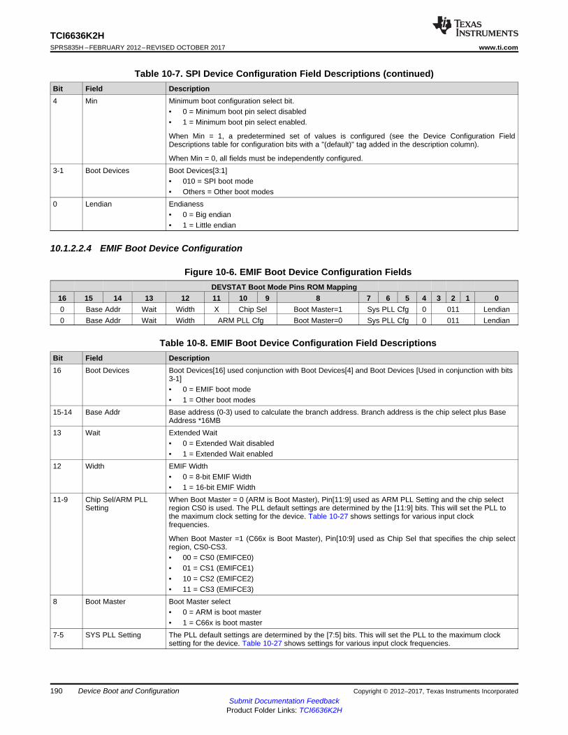
190
TCI6636K2HSPRS835H –FEBRUARY 2012–REVISED OCTOBER 2017 www.ti.com
Submit Documentation FeedbackProduct Folder Links: TCI6636K2H
Device Boot and Configuration Copyright © 2012–2017, Texas Instruments Incorporated
Table 10-7. SPI Device Configuration Field Descriptions (continued)Bit Field Description4 Min Minimum boot configuration select bit.
• 0 = Minimum boot pin select disabled• 1 = Minimum boot pin select enabled.
When Min = 1, a predetermined set of values is configured (see the Device Configuration FieldDescriptions table for configuration bits with a "(default)" tag added in the description column).
When Min = 0, all fields must be independently configured.3-1 Boot Devices Boot Devices[3:1]
• 010 = SPI boot mode• Others = Other boot modes
0 Lendian Endianess• 0 = Big endian• 1 = Little endian
10.1.2.2.4 EMIF Boot Device Configuration
Figure 10-6. EMIF Boot Device Configuration FieldsDEVSTAT Boot Mode Pins ROM Mapping
16 15 14 13 12 11 10 9 8 7 6 5 4 3 2 1 00 Base Addr Wait Width X Chip Sel Boot Master=1 Sys PLL Cfg 0 011 Lendian0 Base Addr Wait Width ARM PLL Cfg Boot Master=0 Sys PLL Cfg 0 011 Lendian
Table 10-8. EMIF Boot Device Configuration Field DescriptionsBit Field Description16 Boot Devices Boot Devices[16] used conjunction with Boot Devices[4] and Boot Devices [Used in conjunction with bits
3-1]• 0 = EMIF boot mode• 1 = Other boot modes
15-14 Base Addr Base address (0-3) used to calculate the branch address. Branch address is the chip select plus BaseAddress *16MB
13 Wait Extended Wait• 0 = Extended Wait disabled• 1 = Extended Wait enabled
12 Width EMIF Width• 0 = 8-bit EMIF Width• 1 = 16-bit EMIF Width
11-9 Chip Sel/ARM PLLSetting
When Boot Master = 0 (ARM is Boot Master), Pin[11:9] used as ARM PLL Setting and the chip selectregion CS0 is used. The PLL default settings are determined by the [11:9] bits. This will set the PLL tothe maximum clock setting for the device. Table 10-27 shows settings for various input clockfrequencies.
When Boot Master =1 (C66x is Boot Master), Pin[10:9] used as Chip Sel that specifies the chip selectregion, CS0-CS3.• 00 = CS0 (EMIFCE0)• 01 = CS1 (EMIFCE1)• 10 = CS2 (EMIFCE2)• 11 = CS3 (EMIFCE3)
8 Boot Master Boot Master select• 0 = ARM is boot master• 1 = C66x is boot master
7-5 SYS PLL Setting The PLL default settings are determined by the [7:5] bits. This will set the PLL to the maximum clocksetting for the device. Table 10-27 shows settings for various input clock frequencies.

191
TCI6636K2Hwww.ti.com SPRS835H –FEBRUARY 2012–REVISED OCTOBER 2017
Submit Documentation FeedbackProduct Folder Links: TCI6636K2H
Device Boot and ConfigurationCopyright © 2012–2017, Texas Instruments Incorporated
Table 10-8. EMIF Boot Device Configuration Field Descriptions (continued)Bit Field Description4 Boot Devices Boot Devices[4] used conjunction with Boot Devices[16] and Boot Devices [Use din conjunction with bits
3-1]• 0 = EMIF boot mode• 1 = Other boot modes
3-1 Boot Devices Boot Devices[3:1] used in conjunction with Boot Device [4]• 011 = EMIF boot mode• Others = Other boot modes
0 Lendian Endianess• 0 = Big endian• 1 = Little endian
10.1.2.2.5 NAND Boot Device Configuration
Figure 10-7. NAND Boot Device Configuration FieldsDEVSTAT Boot Mode Pins ROM Mapping
16 15 14 13 12 11 10 9 8 7 6 5 4 3 2 1 01 First Block Clear X Chip Sel Boot Master=1 Sys PLL Cfg Min 011 Lendian1 First Block Clear ARM PLL Cfg Boot Master=0 Sys PLL Cfg Min 011 Lendian
Table 10-9. NAND Boot Device Configuration Field DescriptionsBit Field Description16 Boot Devices Boot Devices[16] used conjunction with Boot Devices [3-1]
• 0 = Other boot modes• 1 = NAND boot mode
15-13 First Block First Block. This value is used to calculate the first block read. The first block read is the first block value*16.
12 Clear ClearNAND• 0 = Device is not a ClearNAND (default)• 1 = Device is a ClearNAND
11-9 Chip Sel/ARM PLLSetting
When Boot Master = 0 (ARM is Boot Master), Pin[11:9] used as ARM PLL Setting and the chip selectregion CS2 is used. The PLL default settings are determined by the [11:9] bits. This will set the PLL tothe maximum clock setting for the device. Table 10-27 shows settings for various input clockfrequencies.
When Boot Master =1 (C66x is Boot Master), Pin[10:9] used as Chip Sel that specifies the chip selectregion, CS2-CS5.• 00 = CS2• 01 = CS3• 10 = CS4• 11 = CS5
8 Boot Master Boot Master select• 0 = ARM is boot master (default)• 1 = C66x is boot master
7-5 SYS PLL Setting The PLL default settings are determined by the [7:5] bits. This will set the PLL to the maximum clocksetting for the device. Table 10-27 shows settings for various input clock frequencies.
4 Min Minimum boot pin select. When Min is 1, it means that the BOOTMODE [15:3] pins are don't cares. OnlyBOOTMODE [2:0] pins (DEVSTAT[3:1]) will determine boot. Default values are assigned to values thatwould normally be set by the other BOOTMODE pins when Min is 0.• 0 = Minimum boot pin select disabled• 1 = Minimum boot pin select enabled.
3-1 Boot Devices Boot Devices• 011 = NAND boot mode• Others = Other boot modes

192
TCI6636K2HSPRS835H –FEBRUARY 2012–REVISED OCTOBER 2017 www.ti.com
Submit Documentation FeedbackProduct Folder Links: TCI6636K2H
Device Boot and Configuration Copyright © 2012–2017, Texas Instruments Incorporated
Table 10-9. NAND Boot Device Configuration Field Descriptions (continued)Bit Field Description0 Lendian Endianess
• 0 = Big endian• 1 = Little endian
10.1.2.3 Serial Rapid I/O Boot Device Configuration
The device ID is always set to 0xff (8-bit node IDs) or 0xffff (16 bit node IDs) at power-on reset.
Figure 10-8. Serial Rapid I/O Boot Device Configuration FieldsDEVSTAT Boot Mode Pins ROM Mapping
16 15 14 13 12 11 10 9 8 7 6 5 4 3 2 1 0X Ref Clock Data Rate Lane Setup Boot Master=1 Sys PLL Cfg Min 100 Lendian
Lane Ref Clock Data Rate ARM PLL Cfg Boot Master=0 Sys PLL Cfg Min 100 Lendian
Table 10-10. Serial Rapid I/O Boot Device Configuration Field DescriptionsBit Field Description16 Lane When Boot Master =0 (ARM is Boot Master), Pin[16] is used as Lane.
• 0 = 4 ports, each 1 lane wide (default)• 1 = 2 ports, each 2 lanes wide
When Boot Master =1 (C66x is Boot Master), Pin[16] is reserved.15-14 Ref Clock SRIO Reference clock frequency
• 0 = 125 MHz• 1 = 156.25 MHz (default)• 2 = Reserved• 3 = Reserved
13-12 Data Rate SRIO Data Rate• 0 = 1.25GB• 1 = 2.5GB• 2 = 3.125GB• 3 = 5GB (default)
11-9 Lane Setup/ARM PLLSetting
When Boot Master =0 (ARM is Boot Master), pin[11:9] used as ARM PLL Setting with all lanes enabled.The PLL default settings are determined by the [11:9] bits. This will set the PLL to the maximum clocksetting for the device. The default value is 156.26 MHz. Table 10-27 shows settings for various inputclock frequencies.
When Boot Master =1 (C66x is Boot Master), pin [11:9] are used as Lane Set up.• 0 = 4 ports, each 1 lane wide (default)• 1 = 3 ports, lanes 0, 1 form a 2 lane port, lane 2,3 are single ports• 2 = 3 ports, lanes 0, 1 are single lane ports, lanes 2,3 form a 2 lane port• 3 = 2 ports, lane 0, 1 are one port, lane 2, 3 are a second port• 4 = 1 port, 4 lanes wide• 5-7 = 4 ports, each 1 lane wide
8 Boot Master Boot Master select• 0 = ARM is boot master (default)• 1 = C66x is boot master
7-5 SYS PLL Setting The PLL default settings are determined by the [7:5] bits. This will set the PLL to the maximum clocksetting for the device. Default system reference clock is 156.25 MHz. Table 10-27 shows settings forvarious input clock frequencies. (default = 4)
4 Min Minimum boot configuration select bit.• 0 = Minimum boot pin select disabled• 1 = Minimum boot pin select enabled.
When Min = 1, a predetermined set of values is configured (see the Device Configuration FieldDescriptions table for configuration bits with a "(default)" tag added in the description column).
When Min = 0, all fields must be independently configured.

193
TCI6636K2Hwww.ti.com SPRS835H –FEBRUARY 2012–REVISED OCTOBER 2017
Submit Documentation FeedbackProduct Folder Links: TCI6636K2H
Device Boot and ConfigurationCopyright © 2012–2017, Texas Instruments Incorporated
Table 10-10. Serial Rapid I/O Boot Device Configuration Field Descriptions (continued)Bit Field Description3-1 Boot Devices Boot Devices
• 100 = SRIO boot mode• Others = Other boot modes
0 Lendian Endianess• 0 = Big endian• 1 = Little endian
In SRIO boot mode, both the message mode and DirectIO mode will be enabled by default. If use of thememory reserved for received messages is required and reception of messages cannot be prevented, themaster can disable the message mode by writing to the boot table and generating a boot restart.
10.1.2.4 Ethernet (SGMII) Boot Device Configuration
Figure 10-9. Ethernet (SGMII) Boot Device Configuration FieldsDEVSTAT Boot Mode Pins ROM Mapping
16 15 14 13 12 11 10 9 8 7 6 5 4 3 2 1 0Pa clk Ref Clock Ext Con Lane Setup Boot Master=1 Sys PLL Cfg Min 101 LendianPa clk Ref Clock Ext Con ARM PLL Cfg Boot Master=0 Sys PLL Cfg Min 101 Lendian
Table 10-11. Ethernet (SGMII) Boot Device Configuration Field DescriptionsBit Field Description16 Pa clk PA clock reference
• 0 = PA clocked at the same reference as the core reference• 1 = PA clocked at the same reference as the SerDes reference (default)
15-14 Ref Clock SRIO Reference clock frequency• 0 = 125 MHz• 1 = 156.25 MHz (default)• 2 = Reserved• 3 = Reserved
13-12 Ext Con External connection mode• 0 = MAC to MAC connection, master with auto negotiation• 1 = MAC to MAC connection, slave with auto negotiation (default)• 2 = MAC to MAC, forced link, maximum speed• 3 = MAC to fiber connection
11-9 Lane Setup/ARM PLLSetting
When Boot Master = 0 (ARM is Boot Master), pin[11:9] used as ARM PLL Setting. The PLL defaultsettings are determined by the [11:9] bits. This will set the PLL to the maximum clock setting for thedevice. Table 10-27 shows settings for various input clock frequencies.
When Boot Master =1 (C66x is Boot Master), pin [10:9] are used as Lane Set up.• 0 = All SGMII ports enabled (default)• 1 = Only SGMII port 0 enabled• 2 = SGMII port 0 and 1 enabled• 3 = SGMII port 0, 1 and 2 enabled• 4-7 = Reserved
8 Boot Master Boot Master select• 0 = ARM is boot master (default)• 1 = C66x is boot master
7-5 SYS PLL Setting The PLL default settings are determined by the [7:5] bits. This will set the PLL to the maximum clocksetting for the device. Default system reference clock is 156.25 MHz. Table 10-27 shows settings forvarious input clock frequencies. (default = 4)

194
TCI6636K2HSPRS835H –FEBRUARY 2012–REVISED OCTOBER 2017 www.ti.com
Submit Documentation FeedbackProduct Folder Links: TCI6636K2H
Device Boot and Configuration Copyright © 2012–2017, Texas Instruments Incorporated
Table 10-11. Ethernet (SGMII) Boot Device Configuration Field Descriptions (continued)Bit Field Description4 Min Minimum boot configuration select bit.
• 0 = Minimum boot pin select disabled• 1 = Minimum boot pin select enabled.When Min = 1, a predetermined set of values is configured (see the Device Configuration FieldDescriptions table for configuration bits with a "(default)" tag added in the description column).
When Min = 0, all fields must be independently configured.3-1 Boot Devices Boot Devices
• 101 = Ethernet boot mode• Others = Other boot modes
0 Lendian Endianess• 0 = Big endian• 1 = Little endian
10.1.2.4.1 PCIe Boot Device Configuration
Figure 10-10. PCIe Boot Device Configuration FieldsDEVSTAT Boot Mode Pins ROM Mapping
16 15 14 13 12 11 10 9 8 7 6 5 4 3 2 1 0Ref clk Bar Config Reserved Boot Master=1 Sys PLL Cfg 0110 LendianRef clk Bar Config ARM PLL Cfg Boot Master=0 Sys PLL Cfg 0110 Lendian
Table 10-12. PCIe Boot Device Configuration Field DescriptionsBit Field Description16 Ref clk PCIe Reference clock frequency
• 0 = 100MHz• 1 = Reserved
15-12 Bar Config PCIe BAR registers configuration
This value can range from 0 to 0xf. See Table 10-13.11-9 Reserved/ARM PLL
SettingWhen Boot Master =0 (ARM is Boot Master), pin[11:9] used as ARM PLL Setting. The PLL defaultsettings are determined by the [11:9] bits. This will set the PLL to the maximum clock setting for thedevice. Table 10-27 shows settings for various input clock frequencies.
When Boot Master =1 (C66x is Boot Master), pin [10:9] are reserved.8 Boot Master Boot Master select
• 0 = ARM is boot master (default)• 1 = C66x is boot master
7-5 SYS PLL Setting The PLL default settings are determined by the [7:5] bits. This will set the PLL to the maximum clocksetting for the device. Default system reference clock is 156.25 MHz. Table 10-27 shows settings forvarious input clock frequencies.
4-1 Boot Devices Boot Devices[4:1]• 0110 = PCIe boot mode• Others = Other boot modes
0 Lendian Endianess• 0 = Big endian• 1 = Little endian

195
TCI6636K2Hwww.ti.com SPRS835H –FEBRUARY 2012–REVISED OCTOBER 2017
Submit Documentation FeedbackProduct Folder Links: TCI6636K2H
Device Boot and ConfigurationCopyright © 2012–2017, Texas Instruments Incorporated
Table 10-13. BAR Config / PCIe Window Sizes
BAR CFG BAR032-BIT ADDRESS TRANSLATION
64-BIT ADDRESSTRANSLATION
BAR1 BAR2 BAR3 BAR4 BAR5 BAR2/3 BAR4/50b0000 PCIe MMRs 32 32 32 32
Clone ofBAR4
0b0001 16 16 32 640b0010 16 32 32 640b0011 32 32 32 640b0100 16 16 64 640b0101 16 32 64 640b0110 32 32 64 640b0111 32 32 64 1280b1000 64 64 128 2560b1001 4 128 128 1280b1010 4 128 128 2560b1011 4 128 256 2560b1100 256 2560b1101 512 5120b1110 1024 10240b1111 2048 2048
10.1.2.4.2 HyperLink Boot Device Configuration
Figure 10-11. HyperLink Boot Device Configuration FieldsDEVSTAT Boot Mode Pins ROM Mapping
16 15 14 13 12 11 10 9 8 7 6 5 4 3 2 1 0Port RefClk Data Rate Reserved Boot Master=1 Sys PLL Cfg 1110 LendianPort RefClk Data Rate ARM PLL Cfg Boot Master=0 Sys PLL Cfg 1110 Lendian
Table 10-14. HyperLink Boot Device Configuration Field DescriptionsBit Field Description16 Port HyperLink port
• 0 = HyperLink0• 1 = HyperLink1
15-14 Ref Clocks HyperLink reference clock configuration• 0 = 125 MHz• 1 = 156.25 MHz• 2-3 = Reserved
13-12 Data Rate HyperLink data rate configuration• 0 = 1.25 GBs• 1 = 3.125 GBs• 2 = 6.25 GBs• 3 = 12.5 GBs
11-9 Reserved/ARMPLL Setting
When Boot Master =0 (ARM is Boot Master), pin[11:9] used as ARM PLL Setting. The PLL default settings aredetermined by the [11:9] bits. This will set the PLL to the maximum clock setting for the device. Table 10-27shows settings for various input clock frequencies.
When Boot Master =1 (C66x is Boot Master), pin [10:9] are reserved.8 Boot Master Boot Master select
• 0 = ARM is boot master (default)• 1 = C66x is boot master

196
TCI6636K2HSPRS835H –FEBRUARY 2012–REVISED OCTOBER 2017 www.ti.com
Submit Documentation FeedbackProduct Folder Links: TCI6636K2H
Device Boot and Configuration Copyright © 2012–2017, Texas Instruments Incorporated
Table 10-14. HyperLink Boot Device Configuration Field Descriptions (continued)Bit Field Description7-5 SYS PLL
SettingThe PLL default settings are determined by the [7:5] bits. This will set the PLL to the maximum clock setting forthe device. Default system reference clock is 156.25 MHz. Table 10-27 shows settings for various input clockfrequencies.
4-1 Boot Devices Boot Devices[4:1]• 1110 = HyperLink boot mode• Others = Other boot modes
0 Lendian Endianess• 0 = Big endian• 1 = Little endian
10.1.2.4.3 UART Boot Device Configuration
Figure 10-12. UART Boot Mode Configuration Field DescriptionDEVSTAT Boot Mode Pins ROM Mapping
16 15 14 13 12 11 10 9 8 7 6 5 4 3 2 1 0X X X X Port X X X Boot Master=1 Sys PLL Config Min 111 LendianX X X X Port ARM PLL Cfg Boot Master=0 Sys PLL Config Min 111 Lendian
Table 10-15. UART Boot Configuration Field DescriptionsBit Field Description16-13 Reserved Not Used12 Port UART Port number
• 0 = UART0• 1 = UART1
11-9 ARM PLLSetting
The PLL default settings are determined by the [11:9] bits. This will set the PLL to the maximum clock setting forthe device. Table 10-27 shows settings for various input clock frequencies.
8 Boot Master Boot Master select• 0 = ARM is boot master• 1 = C66x is boot master
7-5 SYS PLLSetting
The PLL default settings are determined by the [7:5] bits. This will set the PLL to the maximum clock setting forthe device. Table 10-27 shows settings for various input clock frequencies. (default = 4)
4 Min Minimum boot configuration select bit.• 0 = Minimum boot pin select disabled• 1 = Minimum boot pin select enabled.
When Min = 1, a predetermined set of values is configured (see the Device Configuration Field Descriptions tablefor configuration bits with a "(default)" tag added in the description column).
When Min = 0, all fields must be independently configured.3-1 Boot Devices Boot Devices[3:1]
• 111 = UART boot mode• Others = Other boot modes
0 Lendian Endianess• 0 = Big endian• 1 = Little endian
10.1.2.5 Boot Parameter Table
The ROM Bootloader (RBL) uses a set of tables to carry out the boot process. The boot parameter table isthe most common format the RBL employs to determine the boot flow. These boot parameter tables havecertain parameters common across all the boot modes, while the rest of the parameters are unique to theboot modes. The common entries in the boot parameter table are shown in Table 10-16.

197
TCI6636K2Hwww.ti.com SPRS835H –FEBRUARY 2012–REVISED OCTOBER 2017
Submit Documentation FeedbackProduct Folder Links: TCI6636K2H
Device Boot and ConfigurationCopyright © 2012–2017, Texas Instruments Incorporated
Table 10-16. Boot Parameter Table Common Parameters
BYTE OFFSET NAME DESCRIPTION0 Length The length of the table, including the length field, in bytes.2 Checksum The 16 bits ones complement of the ones complement of the entire table. A
value of 0 will disable checksum verification of the table by the boot ROM.4 Boot Mode Internal values used by RBL for different boot modes.6 Port Num Identifies the device port number to boot from, if applicable8 SW PLL, MSW PLL configuration, MSW10 SW PLL, LSW PLL configuration, LSW12 Sec PLL Config, MSW ARM PLL configuration, MSW14 Sec PLL Config, LSW ARM PLL configuration, LSW16 System Freq The frequency of the system clock in MHz18 Core Freq The frequency of the core clock in MHz20 Boot Master Set to TRUE if C66x is the master core.
10.1.2.5.1 EMIF16 Boot Parameter Table
Table 10-17. EMIF16 Boot Parameter Table
BYTE OFFSET NAME DESCRIPTION
CONFIGUREDTHROUGH BOOTCONFIGURATION PINS
22 Options Async Config Parameters are used.• 0 = Value in the async config paramters are not
used to program async config registers.• 1 = Value in the async config paramters are used
to program async config registers.
NO
24 Type Set to 0 for EMIF16 (NOR) boot NO26 Branch Address MSW Most significant bit for Branch address (depends on
chip select)YES
28 Branch Address LSW Least significant bit for Branch address (depends onchip select)
YES
30 Chip Select Chip Select for the NOR flash YES32 Memory Width Memory width of the EMIF16 bus (16 bits) YES34 Wait Enable Extended wait mode enabled
• 0 = Wait enable is disabled• 1 = Wait enable is enabled
YES
36 Async Config MSW Async Config Register MSW NO38 Async Config LSW Async Config Register LSW NO

198
TCI6636K2HSPRS835H –FEBRUARY 2012–REVISED OCTOBER 2017 www.ti.com
Submit Documentation FeedbackProduct Folder Links: TCI6636K2H
Device Boot and Configuration Copyright © 2012–2017, Texas Instruments Incorporated
10.1.2.5.2 SRIO Boot Parameter Table
Table 10-18. SRIO Boot Parameter Table
BYTEOFFSET NAME DESCRIPTION
CONFIGUREDTHROUGH BOOTCONFIGURATION PINS
22 Options Bit 0 Tx enable• 0 = SRIO Transmit disable• 1 = SRIO Transmit Enable
Bit 1 Mailbox Enable• 0 = Mailbox mode disabled. (SRIO boot is in DirectIO mode).• 1 = Mailbox mode enabled. (SRIO boot is in Messaging mode).
Bit 2 Bypass Configuration• 0 = Configure the SRIO• 1 = Bypass SRIO configuration
Bit 3 Bypass QM Configuration• 0 = Configure the QM and CPDMA• 1 = Bypass the QM and CPDMA configuration
Bit 4 PLL setup• 0 = SERDES Configuration registers are taken without modification.• 1 = SERDES Configuration are modified based on the reference clock
and link rate.
Bit 5-15 = Reserved
NO
24 Lane Setup • 0b0000 = SRIO configured as four 1x ports• 0b0001 = SRIO configured as 3 ports (2x, 1x, 1x)• 0b0010 = SRIO configured as 3 ports (1x, 1x, 2x)• 0b0011 =SRIO configured as 2 ports (2x, 2x)• 0b0100 = SRIO configured as 1 4x port• 0b 0101-0bffff = Reserved
YES (but not all lane setupare possible through theboot configuration pins)
26 Reserved Reserved NA28 Node ID The node ID value to set for this device NO30 SerDes ref clk The SerDes reference clock frequency, in 1/100 MHZ YES32 Link Rate Link rate, MHz YES34 PF Low Packet forward address range, low value NO36 PF High Packet Forward address range, high value NO38 Promiscuous Mask The bit is set for each lane/port that is configured as promiscuous NO40 Time-out Sec Number of seconds before time-out. The value 0 disables the time-out. NO44 SERDES Aux, MSW SERDES Auxillary Register Configuration, MSW NO48 SERDES Aux, LSW SERDES Auxillary Register Configuration, LSW NO52 SERDES Rx Lane0
MSWSERDES Rx Configuration, Lane0, MSW NO
56 SERDES Rx Lane0LSW
SERDES Rx Configuration, Lane0, LSW NO
60 SERDES Rx Lane1MSW
SERDES Rx Configuration, Lane1, MSW NO
64 SERDES Rx Lane1LSW
SERDES Rx Configuration, Lane1, LSW NO
68 SERDES Rx Lane2MSW
SERDES Rx Configuration, Lane2, MSW NO
72 SERDES Rx Lane2LSW
SERDES Rx Configuration, Lane2, LSW NO
76 SERDES Rx Lane3MSW
SERDES Rx Configuration, Lane3, MSW NO

199
TCI6636K2Hwww.ti.com SPRS835H –FEBRUARY 2012–REVISED OCTOBER 2017
Submit Documentation FeedbackProduct Folder Links: TCI6636K2H
Device Boot and ConfigurationCopyright © 2012–2017, Texas Instruments Incorporated
Table 10-18. SRIO Boot Parameter Table (continued)
BYTEOFFSET NAME DESCRIPTION
CONFIGUREDTHROUGH BOOTCONFIGURATION PINS
80 SERDES Rx Lane3LSW
SERDES Rx Configuration, Lane3, LSW NO
10.1.2.5.3 Ethernet Boot Parameter Table
Table 10-19. Ethernet Boot Parameter Table
BYTEOFFSET NAME DESCRIPTION
CONFIGUREDTHROUGH BOOTCONFIGURATION PINS
22 Options Bits 02-00 Interface• 000-100 = Reserved• 101 = SGMII• 110 = Reserved• 111 = Reserved
Bits 03 HD• 0 = Half Duplex• 1 = Full Duplex
Bit 4 Skip TX• 0 = Send Ethernet Ready Frame every 3 seconds• 1 = Don't send Ethernet Ready Frame
Bits 06-05 Initialize Config• 00 = Switch, SerDes, SGMII and PASS are configured• 01 = Initialization is not done for the peripherals that are already
enabled and running.• 10 = Reserved• 11 = None of the Ethernet system is configured.
Bits 15-07 Reserved
NO
24 MAC High The 16 MSBs of the MAC address to receive during boot NO26 MAC Med The 16 middle bits of the MAC address to receive during boot NO28 MAC Low The 16 LSBs of the MAC address to receive during boot NO30 Multi MAC High The 16 MSBs of the multicast MAC address to receive during boot NO32 Multi MAC Med The 16 middle bits of the multicast MAC address to receive during
bootNO
34 Multi MAC Low The 16 LSBs of the multicast MAC address to receive during boot NO36 Source Port The source UDP port to accept boot packets from.
A value of 0 will accept packets from any UDP port
NO
38 Dest Port The destination port to accept boot packets on. NO40 Device ID 12 The first 2 bytes of the device ID.
This is typically a string value, and is sent in the Ethernet readyframe
NO
42 Device ID 34 The second 2 bytes of the device ID. NO44 Dest MAC High The 16 MSBs of the MAC destination address used
for the Ethernet ready frame. Default is broadcast.
NO
46 Dest MAC Med The 16 middle bits of the MAC destination address NO48 Dest MAC Low The 16 LSBs of the MAC destination address NO50 Lane Enable One bit per lane.
• 0 = Lane disabled• 1 = Lane enabled

200
TCI6636K2HSPRS835H –FEBRUARY 2012–REVISED OCTOBER 2017 www.ti.com
Submit Documentation FeedbackProduct Folder Links: TCI6636K2H
Device Boot and Configuration Copyright © 2012–2017, Texas Instruments Incorporated
Table 10-19. Ethernet Boot Parameter Table (continued)
BYTEOFFSET NAME DESCRIPTION
CONFIGUREDTHROUGH BOOTCONFIGURATION PINS
52 SGMII Config Bits 0-3 are the config index, bit 4 set if direct config used, bit 5 set ifno configuration done
NO
54 SGMII Control The SGMII control register value NO56 SGMII Adv Ability The SGMII ADV Ability register value NO58 SGMII TX Cfg High The 16 MSBs of the SGMII Tx config register NO60 SGMII TX Cfg Low The 16 LSBs of the SGMII Tx config register NO62 SGMII RX Cfg High The 16 MSBs of the SGMII Rx config register NO64 SGMII RX Cfg Low The 16 LSBs of the SGMII Rx config register NO66 SGMII Aux Cfg High The 16 MSBs of the SGMII Aux config register NO68 SGMII Aux Cfg Low The 16 LSBs of the SGMII Aux config register NO70 PKT PLL Cfg MSW The packet subsystem PLL configuration, MSW NO72 PKT PLL CFG LSW The packet subsystem PLL configuration, LSW NO
10.1.2.5.4 PCIe Boot Parameter Table
Table 10-20. PCIe Boot Parameter Table
BYTEOFFSET NAME DESCRIPTION
CONFIGUREDTHROUGH BOOTCONFIGURATION PINS
22 Options Bits 00 Mode• 0 = Host Mode (Direct boot mode)• 1 = Boot Table Boot Mode
Bits 01 Configuration of PCIe• 0 = PCIe is configured by RBL• 1 = PCIe is not configured by RBL
Bit 03-02 Reserved
Bits 04 Multiplier• 0 = SERDES PLL configuration is done based on SERDES
register values• 1 = SERDES PLL configuration based on the reference clock
values
Bits 05-15 Reserved
NO
24 Address Width PCI address width, can be 32 or 64 YES with in conjunctionwith BAR sizes
26 Link Rate SerDes frequency, in Mbps. Can be 2500 or 5000 NO28 Reference clock Reference clock frequency, in units of 10 kHz. Value values are 10000
(100 MHz), 12500 (125 MHz), 15625 (156.25 MHz), 25000 (250 MHz)and 31250 (312.5 MHz). A value of 0 means that value is already inthe SerDes cfg parameters and will not be computed by the bootROM.
NO
30 Window 1 Size Window 1 size. YES32 Window 2 Size Window 2 size. YES34 Window 3 Size Window 3 size. Valid only if address width is 32. YES36 Window 4 Size Window 4 Size. Valid only if the address width is 32. YES38 Vendor ID Vendor ID NO40 Device ID Device ID NO42 Class code Rev ID
MSWClass code revision ID MSW NO
44 Class code Rev IDLSW
Class code revision ID LSW NO

201
TCI6636K2Hwww.ti.com SPRS835H –FEBRUARY 2012–REVISED OCTOBER 2017
Submit Documentation FeedbackProduct Folder Links: TCI6636K2H
Device Boot and ConfigurationCopyright © 2012–2017, Texas Instruments Incorporated
Table 10-20. PCIe Boot Parameter Table (continued)
BYTEOFFSET NAME DESCRIPTION
CONFIGUREDTHROUGH BOOTCONFIGURATION PINS
46 SerDes cfg msw PCIe SerDes config word, MSW NO48 SerDes cfg lsw PCIe SerDes config word, LSW NO50 SerDes lane 0 cfg msw SerDes lane config word, msw lane 0 NO52 SerDes lane 0 cfg lsw SerDes lane config word, lsw, lane 0 NO54 SerDes lane 1 cfg msw SerDes lane config word, msw, lane 1 NO56 SerDes lane 1 cfg lsw SerDes lane config word, lsw, lane 1 NO58 Time-out period (Secs) The time-out period. Values 0 disables the time-out.
10.1.2.5.5 I2C Boot Parameter Table
Table 10-21. I2C Boot Parameter Table
OFFSET FIELD VALUE
CONFIGUREDTHROUGH BOOTCONFIGURATION PINS
22 Option Bits 02-00 Mode• 000 = Boot Parameter Table Mode• 001 = Boot Table Mode• 010 = Boot Config Mode• 011 = Load GP header format data• 100 = Slave Receive Boot Config
Bits 15-03 Reserved
NO
24 Boot Dev Addr The I2C device address to boot from YES26 Boot Dev Addr
ExtExtended boot device address YES
28 Broadcast Addr I2C address used to send data in the I2C master broadcast mode. NO30 Local Address The I2C address of this device NO34 Bus Frequency The desired I2C data rate (kHz) NO36 Next Dev Addr The next device address to boot (Used only if boot config option is selected) NO38 Next Dev Addr
ExtThe extended next device address to boot (Used only if boot config option isselected)
NO
40 Address Delay The number of CPU cycles to delay between writing the address to an I2CEEPROM and reading data.
NO
10.1.2.5.6 SPI Boot Parameter Table
Table 10-22. SPI Boot Parameter Table
BYTEOFFSET NAME DESCRIPTION
CONFIGUREDTHROUGH BOOTCONFIGURATION PINS
22 Options Bits 01 and 00 Modes• 00 = Load a boot parameter table from the SPI (Default mode)• 01 = Load boot records from the SPI (boot tables)• 10 = Load boot config records from the SPI (boot config tables)• 11 = Load GP header blobBits 15- 02= Reserved
NO
24 Address Width The number of bytes in the SPI device address. Can be 16 or 24 bit YES26 NPin The operational mode, 4 or 5 pin YES28 Chipsel The chip select used (valid in 4 pin mode only). Can be 0-3. YES30 Mode Standard SPI mode (0-3) YES32 C2Delay Setup time between chip assert and transaction NO

202
TCI6636K2HSPRS835H –FEBRUARY 2012–REVISED OCTOBER 2017 www.ti.com
Submit Documentation FeedbackProduct Folder Links: TCI6636K2H
Device Boot and Configuration Copyright © 2012–2017, Texas Instruments Incorporated
Table 10-22. SPI Boot Parameter Table (continued)
BYTEOFFSET NAME DESCRIPTION
CONFIGUREDTHROUGH BOOTCONFIGURATION PINS
34 Bus Freq, 100kHz The SPI bus frequency in kHz. NO36 Read Addr MSW The first address to read from, MSW (valid for 24 bit address width only) YES38 Read Addr LSW The first address to read from, LSW YES40 Next Chip Select Next Chip Select to be used (Used only in boot Config mode) NO42 Next Read Addr MSW The Next read address (used in boot config mode only) NO44 Next Read Addr LSW The Next read address (used in boot config mode only) NO
10.1.2.5.7 HyperLink Boot Parameter Table
Table 10-23. HyperLink Boot Parameter Table
BYTEOFFSET NAME DESCRIPTION
CONFIGURED THROUGHBOOT CONFIGURATIONPINS
12 Options Bits 00 Reserved
Bits 01 Configuration of Hyperlink• 0 = HyperLink is configured by RBL• 1 = HyperLink is not configured by RBLBits 15-02 = Reserved
NO
14 Number of Lanes Number of Lanes to be configured NO16 SerDes cfg msw PCIe SerDes config word, MSW NO18 SerDes cfg lsw PCIe SerDes config word, LSW NO20 SerDes CFG RX lane 0 cfg msw SerDes RX lane config word, msw lane 0 NO22 SerDes CFG RXlane 0 cfg lsw SerDes RX lane config word, lsw, lane 0 NO24 SerDes CFG TX lane 0 cfg msw SerDes TX lane config word, msw lane 0 NO26 SerDes CFG TXlane 0 cfg lsw SerDes TX lane config word, lsw, lane 0 NO28 SerDes CFG RX lane 1 cfg msw SerDes RX lane config word, msw lane 1 NO30 SerDes CFG RXlane 1 cfg lsw SerDes RX lane config word, lsw, lane 1 NO32 SerDes CFG TX lane 1 cfg msw SerDes TX lane config word, msw lane 1 NO34 SerDes CFG TXlane 1 cfg lsw SerDes TX lane config word, lsw, lane 1 NO36 SerDes CFG RX lane 2 cfg msw SerDes RX lane config word, msw lane 2 NO38 SerDes CFG RXlane 2 cfg lsw SerDes RX lane config word, lsw, lane 2 NO40 SerDes CFG TX lane 2 cfg msw SerDes TX lane config word, msw lane 2 NO42 SerDes CFG TXlane 2 cfg lsw SerDes TX lane config word, lsw, lane 2 NO44 SerDes CFG RX lane 3 cfg msw SerDes RX lane config word, msw lane 3 NO46 SerDes CFG RXlane 3 cfg lsw SerDes RX lane config word, lsw, lane 3 NO48 SerDes CFG TX lane 3 cfg msw SerDes TX lane config word, msw lane 3 NO50 SerDes CFG TXlane 3 cfg lsw SerDes TX lane config word, lsw, lane 3 NO
10.1.2.5.8 UART Boot Parameter Table
Table 10-24. UART Boot Parameter Table
BYTEOFFSET NAME DESCRIPTION
CONFIGURED THROUGHBOOT CONFIGURATIONPINS
22 Reserved None NA

203
TCI6636K2Hwww.ti.com SPRS835H –FEBRUARY 2012–REVISED OCTOBER 2017
Submit Documentation FeedbackProduct Folder Links: TCI6636K2H
Device Boot and ConfigurationCopyright © 2012–2017, Texas Instruments Incorporated
Table 10-24. UART Boot Parameter Table (continued)
BYTEOFFSET NAME DESCRIPTION
CONFIGURED THROUGHBOOT CONFIGURATIONPINS
24 Data Format Bits 00 Data Format• 0 = Data Format is BLOB• 1 = Data Format is Boot TableBits 15-01 Reserved
NO
26 Protocol Bits 00 Protocol• 0 = Xmodem Protocol• 1 = ReservedBits 15-01 Reserved
NO
28 Initial NACK Count Number of NACK pings to be sent before giving up NO30 Max Err Count Maximum number of consecutive receive errors acceptable. NO32 NACK Time-out Time (ms) waiting for NACK/ACK. NO34 Character Time-out Time Period between characters NO36 nDatabits Number of bits supported for data. Only 8 bits is supported. NO38 Parity Bits 01-00 Parity
• 00 = No Parity• 01 = Odd parity• 10 = Even ParityBits 15-02 Reserved
NO
40 nStopBitsx2 Number of stop bits times two. Valid values are 2 (stop bits = 1), 3 (StopBits = 1.5), 4 (Stop Bits = 2)
NO
42 Over sample factor The over sample factor. Only 13 and 16 are valid. NO44 Flow Control Bits 00 Flow Control
• 0 = No Flow Control• 1 = RTS_CTS flow controlBits 15-01 Reserved
NO
46 Data Rate MSW Baud Rate, MSW NO48 Data Rate LSW Baud Rate, LSW NO
10.1.2.5.9 NAND Boot Parameter Table
Table 10-25. NAND Boot Parameter Table
BYTE OFFSET NAME DESCRIPTIONCONFIGURED THROUGHBOOT CONFIGURATION PINS
22 Options Bits 00 Geometry• 0 = Geometry is taken from this table• 1 = Geometry is queried from NAND device.Bits 01 Clear NAND• 0 = NAND Device is a non clear NAND and
requires ECC• 1 = NAND is a clear NAND and doesn.t need
ECC.Bits 15-02 Reserved
NO
24 numColumnAddrBytes Number of bytes used to specify column address NO26 numRowAddrBytes Number of bytes used to specify row address. NO28 numofDataBytesperPage_msw Number of data bytes in each page, MSW NO30 numofDataBytesperPage_lsw Number of data bytes in each page, LSW NO32 numPagesperBlock Number of Pages per Block NO34 busWidth EMIF bus width. Only 8 or 16 bits is supported. NO36 numSpareBytesperPage Number of spare bytes allocated per page. NO38 csel Chip Select number (valid chip selects are 2-5) YES (If ARM is the boot master
only chip select 2 is supported)

204
TCI6636K2HSPRS835H –FEBRUARY 2012–REVISED OCTOBER 2017 www.ti.com
Submit Documentation FeedbackProduct Folder Links: TCI6636K2H
Device Boot and Configuration Copyright © 2012–2017, Texas Instruments Incorporated
Table 10-25. NAND Boot Parameter Table (continued)
BYTE OFFSET NAME DESCRIPTIONCONFIGURED THROUGHBOOT CONFIGURATION PINS
40 First Block First block for RBL to try to read. YES
10.1.2.5.10 DDR3 Configuration Table
The RBL also provides an option to configure the DDR table before loading the image into the externalmemory. More information on how to configure the DDR3, see the KeyStone Architecture DSP BootloaderUser's Guide. The configuration table for DDR3 is shown in Table 10-26
Table 10-26. DDR3 Boot Parameter
BYTE OFFSET NAME DESCRIPTION0 Enable bitmap MSW Bits 31:0 of the PLL/EMIF enable bitmap. Bit 0 corresponds to the PLL config,
Bit 1 to the SDRAM configuration register. There are 24 valid bits in this field(with the MSB corresponding to Rw/exc thresh).
4 Enable bitmap SLSW Bits 31:0 of the chip level register enable bit map. Bit 0 corresponds to chiplevel configuration register 0.
8 Enable bitmap LSW Bits 60:32 of the chip level register enable bit map. Bit 0 corresponds to chiplevel configuration register 32.
12 PLL Predivier PLL Predivision (1 = divide by 1, 2 = divide by 2, and so on)16 PLL Multiplier PLL Multiplication20 PLL Post Divider PLL Postdivision24 sdRamConfig SDRAM Configuration Register28 Refresh ctl SDRAM Refresh Control Register32 Timing 1 SDRAM Timing 1 Register36 Timing 2 SDRAM Timing 2 Register40 Timing 3 SDRAM Timing 3 Register44 Timing4 SDRAM Timing 4 Register48 Pwr management Power Management Control Register52 Vbus M cfg VBUS M Configuration56 Vbus M cfg val 1 VBUS M Configuration Value 160 Vbus M cfg val 2 VBUSM Configuration Value 264 IO DFT Test I/O DFT test logic control68 Perf ctl sel Performance Counter Master Region Select Register72 Perf cnt Mst Reg Performance Count Master Region Select76 Zq config SDRAM Output Impedance Calibration Configuration Register80 Pri Class Svc Map Priority class Service Map84 Mst Id class 1 Master ID class service map 188 Mst Id class 2 Master ID class service map 292 ECC ctrl ECC Control Register96 ECC addr rng 1 ECC Address Range 1 Register100 ECC addr rng 2 ECC Address Range 2 Register104 Rw/exc thresh Read Write Execution Threshold Register108 PHY PIR PHY PIR register (SLSW mask bit 0)112 PHY PGCR0 PHY PGCR0 register (SLSW mask bit 1)116 PHY PGCR1 PHY PGCR1 register (SLSW mask bit 2)120 PHY PGCR2 PHY PGCR2 register (SLSW mask bit 3)124 PHY PGSR0 PHY PGSR0 register (SLSW mask bit 4)128 PHY PGSR1 PHY PGSR1 register (SLSW mask bit 5)132 PHY PTR0 PHY PTR 0 register (SLSW mask bit 6)136 PHY PTR1 PHY PTR 1 register (SLSW mask bit 7)

205
TCI6636K2Hwww.ti.com SPRS835H –FEBRUARY 2012–REVISED OCTOBER 2017
Submit Documentation FeedbackProduct Folder Links: TCI6636K2H
Device Boot and ConfigurationCopyright © 2012–2017, Texas Instruments Incorporated
Table 10-26. DDR3 Boot Parameter (continued)BYTE OFFSET NAME DESCRIPTION140 PHY PTR2 PHY PTR 2 register (SLSW mask bit 8)144 PHY PTR3 PHY PTR 3 register (SLSW mask bit 9)148 PHY PTR4 PHY PTR 4 register (SLSW mask bit 10)152 PHY DCR PHY DCR register (SLSW mask bit 11)156 PHY DTPR0 PHY DTPR 0 register (SLSW mask bit 12)160 PHY DTPR1 PHY DTPR 1 register (SLSW mask bit 13)164 PHY DTPR2 PHY DTPR 2 register (SLSW mask bit 14)168 PHY MR0 PHY MR 0 register (SLSW mask bit 15)172 PHY MR1 PHY MR 1 register (SLSW mask bit 16)176 PHY MR2 PHY MR 2 register (SLSW mask bit 17)180 PHY DTCR PHY DTCR register (SLSW mask bit 18)184 PHY DX0GCR PHY DX 0 GCR register (SLSW mask bit 19)188 PHY DX1GCR PHY DX 1 GCR register (SLSW mask bit 20)192 PHY DX2GCR PHY DX 2 GCR register (SLSW mask bit 21)196 PHY DX3GCR PHY DX 3 GCR register (SLSW mask bit 22)200 PHY DX4CGR PHY DX 4 GCR register (SLSW mask bit 23)204 PHY DX5GCR PHY DX 5 GCR register (SLSW mask bit 24)208 PHY DX6GCR PHY DX 6 GCR register (SLSW mask bit 25)212 PHY DX7GCR PHY DX 7 GCR register (SLSW mask bit 26)216 PHY DX8GCR PHY DX 8 GCR register (SLSW mask bit 27)
10.1.2.6 Second-Level Bootloaders
Any of the boot modes can be used to download a second-level bootloader. A second-level bootloaderallows for:• Any level of customization to current boot methods• Definition of a completely customized boot
10.1.3 SoC SecurityThe TI SoC contains security architecture that allows the C66x CorePacs and ARM CorePac to performsecure accesses within the device. For more information, contact a TI sales office for additionalinformation available with the purchase of a secure device.
10.1.4 System PLL SettingsThe PLL default settings are determined by the BOOTMODE[7:5] bits. Table 10-27 shows the settings forvarious input clock frequencies. This will set the PLL to the maximum clock setting for the device.
CLK = CLKIN × ((PLLM+1) ÷ ((CLKOD+1) × (PLLD+1)))(1)
Where OUTPUT_DIVIDE is the value of the field of SECCTL[22:19]
The configuration for the PASS PLL is also shown. The PASS PLL is configured with these values only ifthe Ethernet boot mode is selected with the input clock set to match the main PLL clock (not the SGMIISerDes clock). See Table 10-11 for details on configuring Ethernet boot mode. The output from the PASSPLL goes through an on-chip divider to reduce the frequency before reaching the NETCP. The PASS PLLgenerates 1050 MHz, and after the chip divider (/3), applies 350 MHz to the NETCP.
The Main PLL is controlled using a PLL controller and a chip-level MMR. The ARM CorePac PLL, DDR3APLL, DDR3BPLL, and PASS PLL are controlled by chip level MMRs. For details on how to set up the PLLsee Section 11.5. For details on the operation of the PLL controller module, see the KeyStone ArchitecturePhase Locked Loop (PLL) Controller User's Guide.

206
TCI6636K2HSPRS835H –FEBRUARY 2012–REVISED OCTOBER 2017 www.ti.com
Submit Documentation FeedbackProduct Folder Links: TCI6636K2H
Device Boot and Configuration Copyright © 2012–2017, Texas Instruments Incorporated
(1) The CLKOD reset value = 1, and the value of 1 is used for all calculations in this table (based on Equation 1).
(2) The PASS PLL generates 1050 MHz and is internally divided by 3 to feed 350 MHz to the packet accelerator.(3) ƒ represents frequency in MHz.
Table 10-27. System PLL Configuration
BOOTMODE[7:5]
INPUTCLOCKFREQ(MHz) (1)
800-MHz DEVICE 1000-MHz DEVICE 1200-MHz DEVICE PA = 350 MHz (2)
PLLD PLLM DSP ƒ PLLD PLLM DSP ƒ PLLD PLLM DSP ƒ PLLD PLLM DSP ƒ (3)
0b000 50.00 0 31 800 0 39 1000 0 47 1200 0 41 10500b001 66.67 0 23 800.04 0 29 1000.05 0 35 1200.06 1 62 1050.0530b010 80.00 0 19 800 0 24 1000 0 29 1200 3 104 10500b011 100.00 0 15 800 0 19 1000 0 23 1200 0 20 10500b100 156.25 3 40 800.78 4 63 1000 2 45 1197.92 24 335 10500b101 250.00 4 31 800 0 7 1000 4 47 1200 4 41 10500b110 312.50 7 40 800.78 4 31 1000 2 22 1197.92 24 167 10500b111 122.88 0 12 798.72 3 64 999.989 0 19 1228.80 11 204 1049.6
(1) The CLKOD reset value = 1, and the value of 1 is used for all calculations in this table (based on Equation 2).
(2) ƒ represents frequency in MHz.
10.1.4.1 ARM CorePac System PLL Settings
The PLL default settings are determined by the BOOTMODE[11:9] bits. Table 10-28 shows settings forvarious input clock frequencies. This will set the PLL to the maximum clock setting for the device.
CLK = CLKIN × ((PLLM+1) ÷ ((CLKOD+1) × (PLLD+1))) (2)
The ARM CorePac PLL is controlled using a PLL controller and a chip-level MMR. For details on how toset up the PLL see Section 11.5. For details on the operation of the PLL controller module, see theKeyStone Architecture Phase Locked Loop (PLL) Controller User's Guide.
Table 10-28. ARM PLL Configuration
BOOTMODE[11:9]
INPUTCLOCKFREQ(MHz) (1)
800-MHz DEVICE 1000-MHz DEVICE 1200-MHz DEVICE 1400-MHz DEVICE
PLLD PLLMARMƒ PLLD PLLM ARM ƒ PLLD PLLM ARM ƒ PLLD PLLM
ARMƒ (2)
0b000 50.00 0 31 800 0 39 1000 0 47 1200 0 55 14000b001 66.67 0 23 800.04 0 29 1000.05 0 35 1200.06 0 41 1400.070b010 80.00 0 19 800 0 24 1000 0 29 1200 0 34 14000b011 100.00 0 15 800 0 19 1000 0 23 1200 0 27 14000b100 156.25 3 40 800.78 4 63 1000 2 45 1197.92 0 17 1406.250b101 250.00 4 31 800 0 7 1000 4 47 1200 4 55 14000b110 312.50 7 40 800.78 4 31 1000 2 22 1197.92 0 8 1406.250b111 122.88 0 12 798.72 3 64 999.40 0 19 1200.80 0 22 1413.12
10.2 Device ConfigurationCertain device configurations like boot mode and endianess are selected at device power-on reset. Thestatus of the peripherals (enabled/disabled) is determined after device power-on reset. By default, theperipherals on the device are disabled and need to be enabled by software before being used.

207
TCI6636K2Hwww.ti.com SPRS835H –FEBRUARY 2012–REVISED OCTOBER 2017
Submit Documentation FeedbackProduct Folder Links: TCI6636K2H
Device Boot and ConfigurationCopyright © 2012–2017, Texas Instruments Incorporated
(1) Internal 100-μA pulldown or pullup is provided for this terminal. In most systems, a 1-kΩ resistor can be used to oppose the IPD/IPU.For more detailed information on pulldown/pullup resistors and situations in which external pulldown/pullup resistors are required, seeSection 4.4.
(2) These signal names are the secondary functions of these pins.
10.2.1 Device Configuration at Device ResetThe logic level present on each device configuration pin is latched at power-on reset to determine thedevice configuration. The logic level on the device configuration pins can be set by using externalpullup/pulldown resistors or by using some control device (for example, FPGA/CPLD) to intelligently drivethese pins. When using a control device, care should be taken to ensure there is no contention on thelines when the device is out of reset. The device configuration pins are sampled during power-on resetand are driven after the reset is removed. To avoid contention, the control device must stop driving thedevice configuration pins of the SoC. Table 10-29 describes the device configuration pins.
NOTEIf a configuration pin must be routed out from the device and it is not driven (Hi-Z state), theinternal pullup/pulldown (IPU/IPD) resistor should not be relied upon. TI recommends the useof an external pullup/pulldown resistor. For more detailed information on pullup/pulldownresistors and situations in which external pullup/pulldown resistors are required, seeSection 4.4.
Table 10-29. Device Configuration Pins
CONFIGURATION PIN PIN NO. IPD/IPU (1) DESCRIPTIONLENDIAN (1) (2) F29 IPU Device endian mode (LENDIAN)
• 0 = Device operates in big endian mode• 1 = Device operates in little endian mode
BOOTMODE[15:0] (1) (2) B30, D29, A35, B29,E29, D30, C30, A30,G30, F31, E30, F30,A31, F24, E24, D24
IPD Method of boot• See Section 10.1.2 for more details.• See the KeyStone Architecture DSP Bootloader User's Guide for
detailed information on boot configuration.AVSIFSEL[1:0] (1) (2) M1, M2 IPD AVS interface selection
• 00 = AVS 4-pin 6-bit Dual-Phase VCNTL[5:2] (Default)• 01 = AVS 4-pin 4-bit Single-Phase VCNTL[5:2]• 10 = AVS 6-pin 6-bit Single-Phase VCNTL[5:0]• 11 = I2C
MAINPLLODSEL (1) (2) E32 IPD Main PLL Output divider select• 0 = Main PLL output divider needs to be set to 2 by BOOTROM• 1 = Reserved
ARMAVSSHARED (1) G24 IPD ARM AVS Shared with the rest of SOC AVS• 0 = Reserved• 1 = ARM Core voltage and rest of SoC core voltage shared
BOOTMODE_RSVD (1) B31 IPD Boot mode reserved. Pulldown resistor required on pin.DDR3A_MAP_EN (1) A36 IPD Control ARM remapping of DDR3A address space in the lower 4GB
(32b space) Mode select• 0 = DDR3A memory is accessible from ARM at 0x08 0000 0000-
0x09 FFFF FFFF.• 1 = DDR3A memory is accessible from ARM at 0x00 8000 0000-
0x00 FFFF FFFF with 0x00 8000 0000-0x00 FFFF FFFF aliased at0x08 0000 0000-0x08 7FFF FFFF.

208
TCI6636K2HSPRS835H –FEBRUARY 2012–REVISED OCTOBER 2017 www.ti.com
Submit Documentation FeedbackProduct Folder Links: TCI6636K2H
Device Boot and Configuration Copyright © 2012–2017, Texas Instruments Incorporated
10.2.2 Peripheral Selection After Device ResetSeveral of the peripherals on the TCI6636K2H are controlled by the Power Sleep Controller (PSC). Bydefault, the PCIe, SRIO, HyperLink, RAC, TAC, FFTC, AIF2, TCP3d, TCP3e, and VCP are held in resetand clock-gated. The memories in these modules are also in a low-leakage sleep mode. Software isrequired to turn these memories on. Then, the software enables the modules (turns on clocks anddeasserts reset) before these modules can be used.
If one of the above modules is used in the selected ROM boot mode, the ROM code automaticallyenables the module.
All other modules come up enabled by default and there is no special software sequence to enable. Formore detailed information on the PSC usage, see the KeyStone Architecture Power Sleep Controller(PSC) User's Guide.
10.2.3 Device State Control RegistersThe TCI6636K2H device has a set of registers that are used to control the status of its peripherals. Theseregisters are shown in Table 10-30.
Table 10-30. Device State Control Registers
ADDRESSSTART
ADDRESSEND SIZE ACRONYM DESCRIPTION
0x02620000 0x02620007 8B Reserved0x02620008 0x02620017 16B Reserved0x02620018 0x0262001B 4B JTAGID See Section 10.2.3.30x0262001C 0x0262001F 4B Reserved0x02620020 0x02620023 4B DEVSTAT See Section 10.2.3.10x02620024 0x02620037 20B Reserved0x02620038 0x0262003B 4B KICK0
See Section 10.2.3.40x0262003C 0x0262003F 4B KICK10x02620040 0x02620043 4B DSP_BOOT_ADDR0 The boot address for C66x CorePac0. See Section 10.2.3.50x02620044 0x02620047 4B DSP_BOOT_ADDR1 The boot address for C66x CorePac1. See Section 10.2.3.50x02620048 0x0262004B 4B DSP_BOOT_ADDR2 The boot address for C66x CorePac2. See Section 10.2.3.50x0262004C 0x0262004F 4B DSP_BOOT_ADDR3 The boot address for C66x CorePac3. See Section 10.2.3.50x02620050 0x02620053 4B DSP_BOOT_ADDR4 The boot address for C66x CorePac4. See Section 10.2.3.50x02620054 0x02620057 4B DSP_BOOT_ADDR5 The boot address for C66x CorePac5. See Section 10.2.3.50x02620058 0x0262005B 4B DSP_BOOT_ADDR6 The boot address for C66x CorePac6. See Section 10.2.3.50x0262005C 0x0262005F 4B DSP_BOOT_ADDR7 The boot address for C66x CorePac7. See Section 10.2.3.50x02620060 0x026200DF 128B Reserved0x026200E0 0x0262010F 48B Reserved0x02620110 0x02620117 8B MACID See Section 11.170x02620118 0x0262012F 24B Reserved0x02620130 0x02620133 4B LRSTNMIPINSTAT_CLR See Section 10.2.3.70x02620134 0x02620137 4B RESET_STAT_CLR See Section 10.2.3.90x02620138 0x0262013B 4B Reserved0x0262013C 0x0262013F 4B BOOTCOMPLETE See Section 10.2.3.100x02620140 0x02620143 4B Reserved0x02620144 0x02620147 4B RESET_STAT See Section 10.2.3.80x02620148 0x0262014B 4B LRSTNMIPINSTAT See Section 10.2.3.60x0262014C 0x0262014F 4B DEVCFG See Section 10.2.3.20x02620150 0x02620153 4B PWRSTATECTL See Section 10.2.3.11

209
TCI6636K2Hwww.ti.com SPRS835H –FEBRUARY 2012–REVISED OCTOBER 2017
Submit Documentation FeedbackProduct Folder Links: TCI6636K2H
Device Boot and ConfigurationCopyright © 2012–2017, Texas Instruments Incorporated
Table 10-30. Device State Control Registers (continued)ADDRESSSTART
ADDRESSEND SIZE ACRONYM DESCRIPTION
0x02620154 0x02620157 4B Reserved0x02620158 0x0262015B 4B Reserved0x0262015C 0x0262015F 4B Reserved0x02620160 0x02620160 4B Reserved0x02620164 0x02620167 4B Reserved0x02620168 0x0262016B 4B Reserved0x0262016C 0x0262017F 20B Reserved0x02620180 0x02620183 4B SmartReflex Class0 See Section 11.2.40x02620184 0x0262018F 12B Reserved0x02620190 0x02620193 4B Reserved0x02620194 0x02620197 4B Reserved0x02620198 0x0262019B 4B Reserved0x0262019C 0x0262019F 4B Reserved0x026201A0 0x026201A3 4B Reserved0x026201A4 0x026201A7 4B Reserved0x026201A8 0x026201AB 4B Reserved0x026201AC 0x026201AF 4B Reserved0x026201B0 0x026201B3 4B Reserved0x026201B4 0x026201B7 4B Reserved0x026201B8 0x026201BB 4B Reserved0x026201BC 0x026201BF 4B Reserved0x026201C0 0x026201C3 4B Reserved0x026201C4 0x026201C7 4B Reserved0x026201C8 0x026201CB 4B Reserved0x026201CC 0x026201CF 4B Reserved0x026201D0 0x026201FF 48B Reserved0x02620200 0x02620203 4B NMIGR0 See Section 10.2.3.120x02620204 0x02620207 4B NMIGR10x02620208 0x0262020B 4B NMIGR20x0262020C 0x0262020F 4B NMIGR30x02620210 0x02620213 4B NMIGR40x02620214 0x02620217 4B NMIGR50x02620218 0x0262021B 4B NMIGR60x0262021C 0x0262021F 4B NMIGR70x02620220 0x0262023F 32B Reserved0x02620240 0x02620243 4B IPCGR0 See Section 10.2.3.130x02620244 0x02620247 4B IPCGR10x02620248 0x0262024B 4B IPCGR20x0262024C 0x0262024F 4B IPCGR30x02620250 0x02620253 4B IPCGR40x02620254 0x02620257 4B IPCGR50x02620258 0x0262025B 4B IPCGR60x0262025C 0x0262025F 4B IPCGR70x02620260 0x02620263 4B IPCGR80x02620264 0x02620267 4B IPCGR90x02620268 0x0262026B 4B IPCGR100x0262026C 0x0262026F 4B IPCGR11

210
TCI6636K2HSPRS835H –FEBRUARY 2012–REVISED OCTOBER 2017 www.ti.com
Submit Documentation FeedbackProduct Folder Links: TCI6636K2H
Device Boot and Configuration Copyright © 2012–2017, Texas Instruments Incorporated
Table 10-30. Device State Control Registers (continued)ADDRESSSTART
ADDRESSEND SIZE ACRONYM DESCRIPTION
0x02620270 0x0262027B 12B Reserved0x0262027C 0x0262027F 4B IPCGRH See Section 10.2.3.150x02620280 0x02620283 4B IPCAR0 See Section 10.2.3.140x02620284 0x02620287 4B IPCAR10x02620288 0x0262028B 4B IPCAR20x0262028C 0x0262028F 4B IPCAR30x02620290 0x02620293 4B IPCAR40x02620294 0x02620297 4B IPCAR50x02620298 0x0262029B 4B IPCAR60x0262029C 0x0262029F 4B IPCAR70x026202A0 0x026202A3 4B IPCAR80x026202A4 0x026202A7 4B IPCAR90x026202A8 0x026202AB 4B IPCAR100x026202AC 0x026202AF 4B IPCAR110x026202B0 0x026202BB 12B Reserved0x026202BC 0x026202BF 4B IPCARH See Section 10.2.3.160x026202C0 0x026202FF 64B Reserved0x02620300 0x02620303 4B TINPSEL See Section 10.2.3.170x02620304 0x02620307 4B TOUTPSEL See Section 10.2.3.180x02620308 0x0262030B 4B RSTMUX0 See Section 10.2.3.190x0262030C 0x0262030F 4B RSTMUX10x02620310 0x02620313 4B RSTMUX20x02620314 0x02620317 4B RSTMUX30x02620318 0x0262031B 4B RSTMUX40x0262031C 0x0262031F 4B RSTMUX50x02620320 0x02620323 4B RSTMUX60x02620324 0x02620327 4B RSTMUX70x02620328 0x0262032B 4B RSTMUX80x0262032C 0x0262032F 4B RSTMUX90x02620330 0x02620333 4B RSTMUX100x02620334 0x02620337 4B RSTMUX110x02620338 0x0262034F 4B Reserved0x02620350 0x02620353 4B MAINPLLCTL0 See Section 11.50x02620354 0x02620357 4B MAINPLLCTL10x02620358 0x0262035B 4B PASSPLLCTL0 See Section 11.70x0262035C 0x0262035F 4B PASSPLLCTL10x02620360 0x02620363 4B DDR3APLLCTL0 See Section 11.60x02620364 0x02620367 4B DDR3APLLCTL10x02620368 0x0262036B 4B DDR3BPLLCTL0 See Section 11.60x0262036C 0x0262036F 4B DDR3BPLLCTL10x02620370 0x02620373 4B ARMPLLCTL0 See Section 10.1.4.10x02620374 0x02620377 4B ARMPLLCTL10x02620378 0x0262039B 132B Reserved0x0262039C 0x0262039F 4B Reserved0x02620400 0x02620403 4B ARMENDIAN_CFG0_0 See Section 10.2.3.210x02620404 0x02620407 4B ARMENDIAN_CFG0_10x02620408 0x0262040B 4B ARMENDIAN_CFG0_2

211
TCI6636K2Hwww.ti.com SPRS835H –FEBRUARY 2012–REVISED OCTOBER 2017
Submit Documentation FeedbackProduct Folder Links: TCI6636K2H
Device Boot and ConfigurationCopyright © 2012–2017, Texas Instruments Incorporated
Table 10-30. Device State Control Registers (continued)ADDRESSSTART
ADDRESSEND SIZE ACRONYM DESCRIPTION
0x0262040C 0x026205FF 62B Reserved0x02620600 0x026206FF 256B Reserved0x02620700 0x02620703 4B CHIP_MISC_CTL0 See Section 10.2.3.240x02620704 0x0262070F 12B Reserved0x02620710 0x02620713 4B SYSENDSTAT See Section 10.2.3.260x02620714 0x02620717 4B Reserved0x02620718 0x0262071B 4B Reserved0x0262071C 0x0262071F 4B Reserved0x02620720 0x0262072F 16B Reserved0x02620730 0x02620733 4B SYNECLK_PINCTL See Section 10.2.3.270x02620734 0x02620737 4B Reserved0x02620738 0x0262074F 24B USB_PHY_CTL See Section 10.2.3.280x02620750 0x026207FF 176B Reserved0x02620800 0x02620C7B 1148B Reserved0x02620C7C 0x02620C7F 4B CHIP_MISC_CTL1 See Section 10.2.3.250x02620C80 0x02620C97 24B Reserved0x02620C90(silicon revision2.0)
0x02620C93(silicon revision2.0)
4B DEVSPEED See Section 10.2.3.20
0x02620C98(silicon revision1.1, 1.0)
0x02620C9B(silicon revision1.1, 1.0)
4B DEVSPEED See Section 10.2.3.20
0x02620C9C 0x02620FFF 868B Reserved
10.2.3.1 Device Status (DEVSTAT) Register
The Device Status register depicts device configuration selected upon a power-on reset by the POR orRESETFULL pin. Once set, these bits remain set until a power-on reset. The Device Status register isshown in Figure 10-13 and described in Table 10-31.
(1) x indicates the bootstrap value latched via the external pin
Figure 10-13. Device Status Register31 30 29 28 27 26 25 24 23 22 21 20 19 18 17 16
Reserved DDR3A_MAP_EN Reserved ARMAVS
SHARED Rsvd MAINPLLODSEL AVSIFSEL BOOT
MODE
R-0000 0000 0000 00 R-x R-x R/W-x R-x R/W-x R/W-xx R/W-xxxxx xxxxxxxx xxx
15 14 13 12 11 10 9 8 7 6 5 4 3 2 1 0
BOOTMODE LENDIAN
R/W-x xxxx xxxx xxxx xxx R-x (1)
Legend: R = Read only; RW = Read/Write; -n = value after reset
Table 10-31. Device Status Register Field DescriptionsBit Field Description31-26 Reserved Reserved. Read only, writes have no effect.25 DDR3A_MAP_EN DDR3A mapping enable
• 0 = DDR3A memory is accessible from ARM at 0x8:0000_0000-0x9:FFFF_FFFF.• 1 = DDR3A memory is accessible in 32b space from ARM, that is, at 0x0:8000_0000-0x0:FFFF_FFFF.
DDR3A is also accessible at 0x8:0000_0000-0x9:FFFF_FFFF, with the space 0x0:8000_0000-0x0:FFFF_FFFF address aliased at 0x8:0000_0000-0x8:7FFF_FFFF.
24-22 Reserved Reserved

212
TCI6636K2HSPRS835H –FEBRUARY 2012–REVISED OCTOBER 2017 www.ti.com
Submit Documentation FeedbackProduct Folder Links: TCI6636K2H
Device Boot and Configuration Copyright © 2012–2017, Texas Instruments Incorporated
Table 10-31. Device Status Register Field Descriptions (continued)Bit Field Description21 ARMAVSSHARED ARM AVS Shared with the rest of SOC AVS
• 0 = Reserved• 1 = ARM Core voltage and rest of SoC core voltage share
20 Reserved Reserved19 MAINPLLODSEL Main PLL Output divider select
• 0 = Main PLL output divider needs to be set to 2 by BOOTROM• 1 = Reserved
18-17 AVSIFSEL AVS interface selection• 00 = AVS 4pin 6bit Dual-Phase VCNTL[5:2] (Default)• 01 = AVS 4pin 4bit Single-Phase VCNTL[5:2]• 10 = AVS 6pin 6bit Single-Phase VCNTL[5:0]• 11 = I2C
16-1 BOOTMODE Determines the boot mode configured for the device. For more information on boot mode, see Section 10.1.2and the KeyStone Architecture DSP Bootloader User's Guide.
0 LENDIAN Device endian mode (LENDIAN) — shows the status of whether the system is operating in big endian modeor little endian mode (default).• 0 = System is operating in big endian mode• 1 = System is operating in little endian mode (default)
10.2.3.2 Device Configuration Register
The Device Configuration Register is one-time writeable through software. The register is reset on all hardresets and is locked after the first write. The Device Configuration Register is shown in Figure 10-14 anddescribed in Table 10-32.
Figure 10-14. Device Configuration Register (DEVCFG)31 30 29 28 27 26 25 24 23 22 21 20 19 18 17 16 15 14 13 12 11 10 9 8 7 6 5 4 3 2 1 0
Reserved PCIESSMODE SYSCLKOUTEN
R-0 R/W-00 R/W-1
Legend: R = Read only; RW = Read/Write; -n = value after reset
Table 10-32. Device Configuration Register Field DescriptionsBit Field Description31-3 Reserved Reserved. Read only, writes have no effect.2-1 PCIESSMODE Device Type Input of PCIeSS
• 00 = Endpoint• 01 = Legacy Endpoint• 10 = Rootcomplex• 11 = Reserved
0 SYSCLKOUTEN SYSCLKOUT enable• 0 = No clock output• 1 = Clock output enabled (default)
10.2.3.3 JTAG ID (JTAGID) Register Description
The JTAG ID register is a read-only register that identifies to the customer the JTAG/Device ID. For thedevice, the JTAG ID register resides at address location 0x02620018. The JTAG ID register is shown inFigure 10-15 and described in Table 10-33.

213
TCI6636K2Hwww.ti.com SPRS835H –FEBRUARY 2012–REVISED OCTOBER 2017
Submit Documentation FeedbackProduct Folder Links: TCI6636K2H
Device Boot and ConfigurationCopyright © 2012–2017, Texas Instruments Incorporated
Figure 10-15. JTAG ID (JTAGID) Register31 30 29 28 27 26 25 24 23 22 21 20 19 18 17 16 15 14 13 12 11 10 9 8 7 6 5 4 3 2 1 0
VARIANT PART NUMBER MANUFACTURER LSB
R-xxxx R-1011 1001 1000 0001 R-0000 0010 111 R-1
LEGEND: R/W = Read/Write; R = Read only; -n = value after reset
Table 10-33. JTAG ID Register Field DescriptionsBit Field Value Description31-28 VARIANT xxxx Variant value27-12 PART NUMBER 1011 1001 1000 0001 Part Number for boundary scan11-1 MANUFACTURER 0000 0010 111 Manufacturer0 LSB 1 This bit is read as a 1
NOTEThe value of the VARIANT and PART NUMBER fields depends on the silicon revision beingused. See the Silicon Errata for details.
10.2.3.4 Kicker Mechanism (KICK0 and KICK1) Register
The Bootcfg module contains a kicker mechanism to prevent spurious writes from changing any of theBootcfg MMR (memory mapped registers) values. When the kicker is locked (which it is initially afterpower on reset), none of the Bootcfg MMRs are writable (they are only readable). This mechanismrequires an MMR write to each of the KICK0 and KICK1 registers with exact data values before the kickerlock mechanism is unlocked. See Table 10-30 for the address location. Once released, all the BootcfgMMRs having write permissions are writable (the read only MMRs are still read only). The KICK0 data is0x83e70b13. The KICK1 data is 0x95a4f1e0. Writing any other data value to either of these kick MMRslocks the kicker mechanism and blocks writes to Bootcfg MMRs. To ensure protection to all BootcfgMMRs, software must always relock the kicker mechanism after completing the MMR writes.
10.2.3.5 DSP Boot Address Register (DSP_BOOT_ADDRn)
The DSP_BOOT_ADDRn register stores the initial boot fetch address of CorePac_n (n = core number).The fetch address is the public ROM base address (for any boot mode) by default. DSP_BOOT_ADDRnregister access should be permitted to any master or emulator when the device is non-secure. CorePacboots from that address when a reset is performed. The DSP_BOOT_ADDRn register is shown inTable 10-34 and described in Table 10-35.
Table 10-34. DSP BOOT Address Register (DSP_BOOT_ADDRn)31
10 9 0
DSP_BOOT_ADDR ReservedRW-0010000010110000000000 R-0
Legend: R = Read only; -n = value after reset
Table 10-35. DSP BOOT Address Register (DSP_BOOT_ADDRn) Field Descriptions
Bit Field Description
31-10 DSP_BOOT_ADDR Boot address of CorePac. CorePac boots from that address when a reset is performed. The resetvalue is 22 MSBs of ROM base address = 0x20B00000.
9-0 Reserved Reserved
10.2.3.6 LRESETNMI PIN Status (LRSTNMIPINSTAT) Register
The LRSTNMIPINSTAT register latches the status of LRESET and NMI. The LRESETNMI PIN Statusregister is shown in Figure 10-16 and described in Table 10-36.

214
TCI6636K2HSPRS835H –FEBRUARY 2012–REVISED OCTOBER 2017 www.ti.com
Submit Documentation FeedbackProduct Folder Links: TCI6636K2H
Device Boot and Configuration Copyright © 2012–2017, Texas Instruments Incorporated
Figure 10-16. LRESETNMI PIN Status Register (LRSTNMIPINSTAT)31 30 29 28 27 26 25 24 23 22 21 20 19 18 17 16 15 14 13 12 11 10 9 8 7 6 5 4 3 2 1 0
Reserved NMI7 NMI6 NMI5 NMI4 NMI3 NMI2 NMI1 NMI0 LR7 LR6 LR5 LR4 LR3 LR2 LR1 LR0
R-0 R-0 R-0 R-0 R-0 R-0 R-0 R-0 R-0 R-0 R-0 R-0 R-0 R-0 R-0 R-0 R-0
Legend: R = Read only; -n = value after reset
Table 10-36. LRESETNMI PIN Status Register Field DescriptionsBit Field Description31-16 Reserved Reserved15 NMI7 C66x CorePac7 in NMI14 NMI6 C66x CorePac6 in NMI13 NMI5 C66x CorePac5 in NMI12 NMI4 C66x CorePac4 in NMI11 NMI3 C66x CorePac3 in NMI10 NMI2 C66x CorePac2 in NMI9 NMI1 C66x CorePac1 in NMI8 NMI0 C66x CorePac0 in NMI7 LR7 C66x CorePac7 in Local Reset6 LR6 C66x CorePac6 in Local Reset5 LR5 C66x CorePac5 in Local Reset4 LR4 C66x CorePac4 in Local Reset3 LR3 C66x CorePac3 in Local Reset2 LR2 C66x CorePac2 in Local Reset1 LR1 C66x CorePac1 in Local Reset0 LR0 C66x CorePac0 in Local Reset
10.2.3.7 LRESETNMI PIN Status Clear (LRSTNMIPINSTAT_CLR) Register
The LRSTNMIPINSTAT_CLR register clears the status of LRESET and NMI. The LRESETNMI PIN StatusClear register is shown in Figure 10-17 and described in Table 10-37.
Figure 10-17. LRESETNMI PIN Status Clear Register (LRSTNMIPINSTAT_CLR)31 30 29 28 27 26 25 24 23 22 21 20 19 18 17 16 15 14 13 12 11 10 9 8 7 6 5 4 3 2 1 0
Reserved NMI7 NMI6 NMI5 NMI4 NMI3 NMI2 NMI1 NMI0 LR7 LR6 LR5 LR4 LR3 LR2 LR1 LR0
R-0 WC-0 WC-0 WC-0 WC-0 WC-0 WC-0 WC-0 WC-0 WC-0 WC-0 WC-0 WC-0 WC-0 WC-0 WC-0 WC-0
Legend: R = Read only; -n = value after reset; WC = Write 1 to Clear
Table 10-37. LRESETNMI PIN Status Clear Register Field DescriptionsBit Field Description31-16 Reserved Reserved15 NMI7 C66x CorePac7 in NMI Clear14 NM6 C66x CorePac6 in NMI Clear13 NMI5 C66x CorePac5 in NMI Clear12 NMI4 C66x CorePac4 in NMI Clear11 NMI3 C66x CorePac3 in NMI Clear10 NMI2 C66x CorePac2 in NMI Clear9 NMI1 C66x CorePac1 in NMI Clear8 NMI0 C66x CorePac0 in NMI Clear7 LR7 C66x CorePac7 in Local Reset Clear6 LR6 C66x CorePac6 in Local Reset Clear5 LR5 C66x CorePac5 in Local Reset Clear

215
TCI6636K2Hwww.ti.com SPRS835H –FEBRUARY 2012–REVISED OCTOBER 2017
Submit Documentation FeedbackProduct Folder Links: TCI6636K2H
Device Boot and ConfigurationCopyright © 2012–2017, Texas Instruments Incorporated
Table 10-37. LRESETNMI PIN Status Clear Register Field Descriptions (continued)Bit Field Description4 LR4 C66x CorePac4 in Local Reset Clear3 LR3 C66x CorePac3 in Local Reset Clear2 LR2 C66x CorePac2 in Local Reset Clear1 LR1 C66x CorePac1 in Local Reset Clear0 LR0 C66x CorePac0 in Local Reset Clear
10.2.3.8 Reset Status (RESET_STAT) Register
The Reset Status register (RESET_STAT) captures the status of local reset (LRx) for each of the coresand also the global device reset (GR). Software can use this information to take different deviceinitialization steps.• In case of local reset: The LRx bits are written as 1 and the GR bit is written as 0 only when the C66x
CorePac receives a local reset without receiving a global reset.• In case of global reset: The LRx bits are written as 0 and the GR bit is written as 1 only when a
global reset is asserted.
The Reset Status register is shown in Figure 10-18 and described in Table 10-38.
Figure 10-18. Reset Status Register (RESET_STAT)31 30 29 28 27 26 25 24 23 22 21 20 19 18 17 16 15 14 13 12 11 10 9 8 7 6 5 4 3 2 1 0
GR Reserved LR7 LR6 LR5 LR4 LR3 LR2 LR1 LR0
R-1 R-000 0000 0000 0000 0000 0000 R-0 R-0 R-0 R-0 R-0 R-0 R-0 R-0
Legend: R = Read only; -n = value after reset
Table 10-38. Reset Status Register Field DescriptionsBit Field Description31 GR Global reset status
• 0 = Device has not received a global reset.• 1 = Device received a global reset.
30-8 Reserved Reserved.7 LR7 C66x CorePac7 reset status
• 0 = C66x CorePac7 has not received a local reset.• 1 = C66x CorePac7 received a local reset.
6 LR6 C66x CorePac6 reset status• 0 = C66x CorePac6 has not received a local reset.• 1 = C66x CorePac6 received a local reset.
5 LR5 C66x CorePac5 reset status• 0 = C66x CorePac5 has not received a local reset.• 1 = C66x CorePac5 received a local reset.
4 LR4 C66x CorePac4 reset status• 0 = C66x CorePac4 has not received a local reset.• 1 = C66x CorePac4received a local reset.
3 LR3 C66x CorePac3 reset status• 0 = C66x CorePac3 has not received a local reset.• 1 = C66x CorePac3 received a local reset.
2 LR2 C66x CorePac2 reset status• 0 = C66x CorePac2 has not received a local reset.• 1 = C66x CorePac2 received a local reset.
1 LR1 C66x CorePac1 reset status• 0 = C66x CorePac1 has not received a local reset.• 1 = C66x CorePac1 received a local reset.
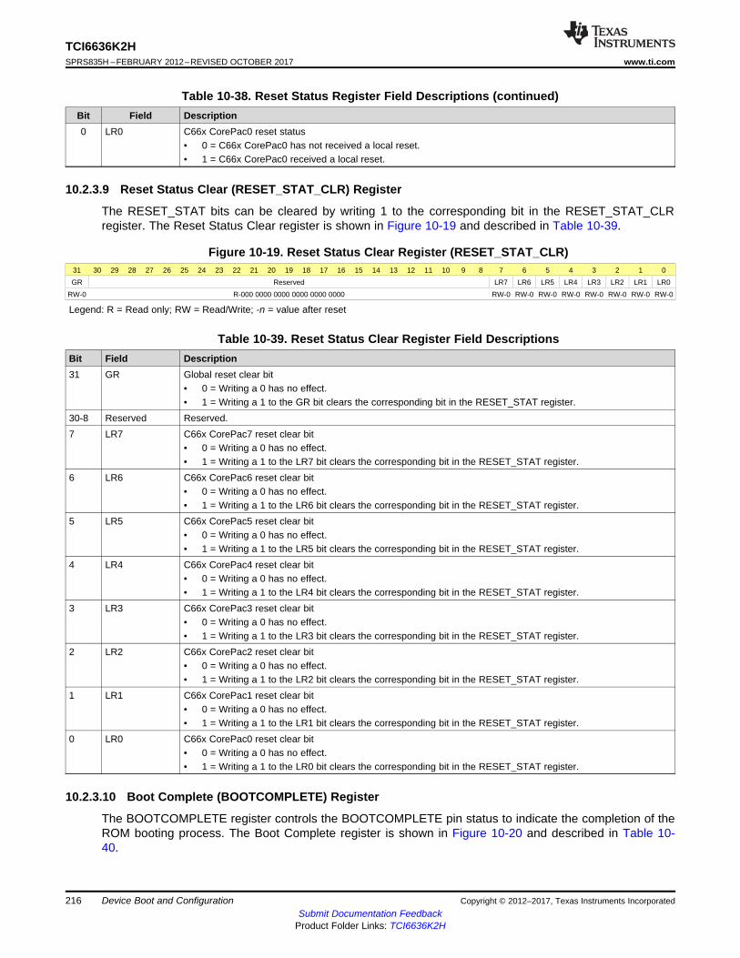
216
TCI6636K2HSPRS835H –FEBRUARY 2012–REVISED OCTOBER 2017 www.ti.com
Submit Documentation FeedbackProduct Folder Links: TCI6636K2H
Device Boot and Configuration Copyright © 2012–2017, Texas Instruments Incorporated
Table 10-38. Reset Status Register Field Descriptions (continued)Bit Field Description0 LR0 C66x CorePac0 reset status
• 0 = C66x CorePac0 has not received a local reset.• 1 = C66x CorePac0 received a local reset.
10.2.3.9 Reset Status Clear (RESET_STAT_CLR) Register
The RESET_STAT bits can be cleared by writing 1 to the corresponding bit in the RESET_STAT_CLRregister. The Reset Status Clear register is shown in Figure 10-19 and described in Table 10-39.
Figure 10-19. Reset Status Clear Register (RESET_STAT_CLR)31 30 29 28 27 26 25 24 23 22 21 20 19 18 17 16 15 14 13 12 11 10 9 8 7 6 5 4 3 2 1 0
GR Reserved LR7 LR6 LR5 LR4 LR3 LR2 LR1 LR0
RW-0 R-000 0000 0000 0000 0000 0000 RW-0 RW-0 RW-0 RW-0 RW-0 RW-0 RW-0 RW-0
Legend: R = Read only; RW = Read/Write; -n = value after reset
Table 10-39. Reset Status Clear Register Field DescriptionsBit Field Description31 GR Global reset clear bit
• 0 = Writing a 0 has no effect.• 1 = Writing a 1 to the GR bit clears the corresponding bit in the RESET_STAT register.
30-8 Reserved Reserved.7 LR7 C66x CorePac7 reset clear bit
• 0 = Writing a 0 has no effect.• 1 = Writing a 1 to the LR7 bit clears the corresponding bit in the RESET_STAT register.
6 LR6 C66x CorePac6 reset clear bit• 0 = Writing a 0 has no effect.• 1 = Writing a 1 to the LR6 bit clears the corresponding bit in the RESET_STAT register.
5 LR5 C66x CorePac5 reset clear bit• 0 = Writing a 0 has no effect.• 1 = Writing a 1 to the LR5 bit clears the corresponding bit in the RESET_STAT register.
4 LR4 C66x CorePac4 reset clear bit• 0 = Writing a 0 has no effect.• 1 = Writing a 1 to the LR4 bit clears the corresponding bit in the RESET_STAT register.
3 LR3 C66x CorePac3 reset clear bit• 0 = Writing a 0 has no effect.• 1 = Writing a 1 to the LR3 bit clears the corresponding bit in the RESET_STAT register.
2 LR2 C66x CorePac2 reset clear bit• 0 = Writing a 0 has no effect.• 1 = Writing a 1 to the LR2 bit clears the corresponding bit in the RESET_STAT register.
1 LR1 C66x CorePac1 reset clear bit• 0 = Writing a 0 has no effect.• 1 = Writing a 1 to the LR1 bit clears the corresponding bit in the RESET_STAT register.
0 LR0 C66x CorePac0 reset clear bit• 0 = Writing a 0 has no effect.• 1 = Writing a 1 to the LR0 bit clears the corresponding bit in the RESET_STAT register.
10.2.3.10 Boot Complete (BOOTCOMPLETE) Register
The BOOTCOMPLETE register controls the BOOTCOMPLETE pin status to indicate the completion of theROM booting process. The Boot Complete register is shown in Figure 10-20 and described in Table 10-40.

217
TCI6636K2Hwww.ti.com SPRS835H –FEBRUARY 2012–REVISED OCTOBER 2017
Submit Documentation FeedbackProduct Folder Links: TCI6636K2H
Device Boot and ConfigurationCopyright © 2012–2017, Texas Instruments Incorporated
Figure 10-20. Boot Complete Register (BOOTCOMPLETE)31 30 29 28 27 26 25 24 23 22 21 20 19 18 17 16 15 14 13 12 11 10 9 8 7 6 5 4 3 2 1 0
Reserved BC11 BC10 BC9 BC8 BC7 BC6 BC5 BC4 BC3 BC BC1 BC0
R,-0000 0000 0000 0000 0000 RW-0 RW-0 RW-0 RW-0 RW-0 RW-0 RW-0 RW-0 RW-0 RW-0 RW-0 RW-0
LEGEND: R/W = Read/Write; R = Read only; -n = value after reset
Table 10-40. Boot Complete Register Field DescriptionsBit Field Description31-12 Reserved Reserved.11 BC11 ARM CorePac 3 boot status
• 0 = ARM CorePac 3 boot NOT complete• 1 = ARM CorePac 3 boot complete
10 BC10 ARM CorePac 2 boot status• 0 = ARM CorePac 2 boot NOT complete• 1 = ARM CorePac 2 boot complete
9 BC9 ARM CorePac 1 boot status• 0 = ARM CorePac 1 boot NOT complete• 1 = ARM CorePac 1 boot complete
8 BC8 ARM CorePac 0 boot status• 0 = ARM CorePac 0 boot NOT complete• 1 = ARM CorePac 0 boot complete
7 BC7 C66x CorePac7 boot status• 0 = C66x CorePac 7 boot NOT complete• 1 = C66x CorePac 7 boot complete
6 BC6 C66x CorePac6 boot status• 0 = C66x CorePac 6 boot NOT complete• 1 = C66x CorePac 6 boot complete
5 BC5 C66x CorePac5 boot status• 0 = C66x CorePac 5 boot NOT complete• 1 = C66x CorePac 5 boot complete
4 BC4 C66x CorePac4 boot status• 0 = C66x CorePac 4 boot NOT complete• 1 = C66x CorePac 4 boot complete
3 BC3 C66x CorePac 3 boot status• 0 = C66x CorePac 3 boot NOT complete• 1 = C66x CorePac 3 boot complete
2 BC2 C66x CorePac2 boot status• 0 = C66x CorePac 2 boot NOT complete• 1 = C66x CorePac 2 boot complete
1 BC1 C66x CorePac1 boot status• 0 = C66x CorePac 1 boot NOT complete• 1 = C66x CorePac 1 boot complete
0 BC0 C66x CorePac0 boot status• 0 = C66x CorePac 0 boot NOT complete• 1 = C66x CorePac 0 boot complete
The BCx bit indicates the boot complete status of the corresponding C66x CorePac. All BCx bits are stickybits — that is, they can be set only once by the software after device reset and they will be cleared to 0 onall device resets (warm reset and power-on reset).
Boot ROM code is implemented such that each C66x CorePac sets its corresponding BCx bit immediatelybefore branching to the predefined location in memory.

218
TCI6636K2HSPRS835H –FEBRUARY 2012–REVISED OCTOBER 2017 www.ti.com
Submit Documentation FeedbackProduct Folder Links: TCI6636K2H
Device Boot and Configuration Copyright © 2012–2017, Texas Instruments Incorporated
10.2.3.11 Power State Control (PWRSTATECTL) Register
The Power State Control register (PWRSTATECTL) is controlled by the software to indicate the power-saving mode. Under ROM code, the C66x CorePac reads this register to differentiate between the variouspower saving modes. This register is cleared only by POR and is not changed by any other device reset.See Hardware Design Guide for KeyStone II Devices for more information. The PWRSTATECTL registeris shown in Figure 10-21 and described in Table 10-41.
Figure 10-21. Power State Control Register (PWRSTATECTL)31 30 29 28 27 26 25 24 23 22 21 20 19 18 17 16 15 14 13 12 11 10 9 8 7 6 5 4 3 2 1 0
Hibernation Recovery Branch Address Width Wait RecoveryMaster
LocalResetAction
StoredSR
Index
HibernationMode Hibernation Rsvd
RW-0000 0000 0000 0000 00 RW-0 RW-0 RW-0 RW-0 RW-0 RW-0 RW-0 R-0
Legend: R = Read Only, RW = Read/Write; -n = value after reset
Table 10-41. Power State Control Register Field DescriptionsBit Field Description31-10 Hibernation
Recovery BranchAddress
Used to provide a start address for execution out of the hibernation modes. See the KeyStone ArchitectureDSP Bootloader User's Guide.
9 Width EMIF16 Width (if the recovery address is in EMIF16 space).• 0 = 8-bit• 1 = 16-bit
8 Wait Extended Wait (if the recovery address is in EMIF16 space)• 0 = Extended Wait disabled• 1 = Extended Wait enabled
7 Recovery Master Master performs hibernation recovery• 0 = C66x CorePacs perform hibernation recovery• 1 = ARM CorePac performs hibernation recovery
6-5 Local Reset Action Action of Local Reset• 00 = Idle on Local Reset• 01 = Branch to the base of MSMC on Local Reset• 10 = Branch to the base of DDR3 on Local Reset• 11 = Branch to the base of L2 on Local Reset (C66x CorePac)
4-3 Stored Index 0-3 value latched in the SR bits of the DEVSTAT register2 Hibernation Mode Indicates whether the device is in hibernation mode 1 or mode 2.
• 0 = Hibernation mode 1• 1 = Hibernation mode 2
1 Hibernation Indicates whether the device is in hibernation mode or not.• 0 = Not in hibernation mode• 1 = Hibernation mode
0 Reserved Reserved
10.2.3.12 NMI Event Generation to C66x CorePac (NMIGRx) Register
NMIGRx registers generate NMI events to the corresponding C66x CorePac. The TCI6636 has eightNMIGRx registers (NMIGR0 through NMIGR7). The NMIGR0 register generates an NMI event to C66xCorePac0, the NMIGR1 register generates an NMI event to C66x CorePac1, and so on. Writing a 1 to theNMIG field generates an NMI pulse. Writing a 0 has no effect and Reads return 0 and have no othereffect. The NMI event generation to the C66x CorePac is shown in Figure 10-22 and described inTable 10-42.

219
TCI6636K2Hwww.ti.com SPRS835H –FEBRUARY 2012–REVISED OCTOBER 2017
Submit Documentation FeedbackProduct Folder Links: TCI6636K2H
Device Boot and ConfigurationCopyright © 2012–2017, Texas Instruments Incorporated
Figure 10-22. NMI Generation Register (NMIGRx)31 30 29 28 27 26 25 24 23 22 21 20 19 18 17 16 15 14 13 12 11 10 9 8 7 6 5 4 3 2 1 0
Reserved NMIG
R-0000 0000 0000 0000 0000 0000 0000 000 RW-0
Legend: RW = Read/Write; -n = value after reset
Table 10-42. NMI Generation Register Field DescriptionsBit Field Description31-1 Reserved Reserved0 NMIG Reads return 0
Writes:• 0 = No effect• 1 = Creates NMI pulse to the corresponding C66x CorePac — C66x CorePac0 for NMIGR0, and so forth.
10.2.3.13 IPC Generation (IPCGRx) Registers
The IPCGRx registers facilitate inter-C66x CorePac interrupts.
The TCI6636K2H device has 12 IPCGRx registers (IPCGR0 through IPCGR11 ). These registers can beused by external hosts or CorePacs to generate interrupts to other CorePacs. A write of 1 to the IPCGfield of the IPCGRx register generates an interrupt pulse to the C66x CorePacx (0 <= x <= 7) or ARMCorePac core (x-8) (8<=x<=11).
These registers also provide a Source ID facility identifying up to 28 different sources of interrupts.Allocation of source bits to source processor and meaning is entirely based on software convention. Theregister field descriptions are given in the following tables. There can be numerous sources for theseregisters as this is completely controlled by software. Any master that has access to BOOTCFG modulespace can write to these registers. The IPC Generation register is shown in Figure 10-23 and described inTable 10-43.
Figure 10-23. IPC Generation Registers (IPCGRx)31 30 29 28 27 26 25 24 23 22 21 20 19 18 17 16 15 14 13 12 11 10 9 8 7 6 5 4 3 2 1 0
SRCS27-SRCS0 Reserved IPCG
RW +0 (per bit field) R-000 RW-0
Legend: R = Read only; RW = Read/Write; -n = value after reset
Table 10-43. IPC Generation Registers Field DescriptionsBit Field Description31-4 SRCSx Reads return current value of internal register bit.
Writes:• 0 = No effect• 1 = Sets both SRCSx and the corresponding SRCCx.
3-1 Reserved Reserved0 IPCG Reads return 0.
Writes:• 0 = No effect• 1 = Creates an inter-DSP/ARM interrupt.

220
TCI6636K2HSPRS835H –FEBRUARY 2012–REVISED OCTOBER 2017 www.ti.com
Submit Documentation FeedbackProduct Folder Links: TCI6636K2H
Device Boot and Configuration Copyright © 2012–2017, Texas Instruments Incorporated
10.2.3.14 IPC Acknowledgment (IPCARx) Registers
The IPCARx registers facilitate inter-CorePac interrupt acknowledgment.
The TCI6636K2H device has 12 IPCARx (IPCAR0 through IPCAR11) registers. These registers alsoprovide a Source ID facility by which up to 28 different sources of interrupts can be identified. Allocation ofsource bits to source processor and meaning is entirely based on software convention. The register fielddescriptions are given in the following tables. Virtually anything can be a source for these registers as thisis completely controlled by software. Any master that has access to BOOTCFG module space can write tothese registers. The IPC Acknowledgment register is shown in Figure 10-24 and described in Table 10-44.
Figure 10-24. IPC Acknowledgment Registers (IPCARx)31 30 29 28 27 26 25 24 23 22 21 20 19 18 17 16 15 14 13 12 11 10 9 8 7 6 5 4 3 2 1 0
SRCC27-SRCC0 Reserved
RW +0 (per bit field) R-0000
Legend: R = Read only; RW = Read/Write; -n = value after reset
Table 10-44. IPC Acknowledgment Registers Field DescriptionsBit Field Description31-4 SRCCx Reads return current value of internal register bit.
Writes:• 0 = No effect• 1 = Clears both SRCCx and the corresponding SRCSx
3-0 Reserved Reserved
10.2.3.15 IPC Generation Host (IPCGRH) Register
The IPCGRH register facilitates interrupts to external hosts. Operation and use of the IPCGRH register isthe same as for other IPCGR registers. The interrupt output pulse created by the IPCGRH registerappears on device pin HOUT.
The host interrupt output pulse is stretched so that it is asserted for four bootcfg clock cycles (SYSCLK1/6)followed by a deassertion of four bootcfg clock cycles. Generating the pulse results in a pulse-blockingwindow that is eight SYSCLK1/6-cycles long. Back-to-back writes to the IPCRGH register with the IPCGbit (bit 0) set, generates only one pulse if the back-to-back writes to IPCGRH are less than the eightSYSCLK1/6 cycle window — the pulse blocking window. To generate back-to-back pulses, the back-to-back writes to the IPCGRH register must be written after the eight SYSCLK1/6 cycle pulse-blockingwindow has elapsed. The IPC Generation Host register is shown in Figure 10-25 and described inTable 10-45.
Figure 10-25. IPC Generation Registers (IPCGRH)31 30 29 28 27 26 25 24 23 22 21 20 19 18 17 16 15 14 13 12 11 10 9 8 7 6 5 4 3 2 1 0
SRCS27-SRCS0 Reserved IPCG
RW +0 (per bit field) R-000 RW+0
Legend: R = Read only; RW = Read/Write; -n = value after reset
Table 10-45. IPC Generation Registers Field DescriptionsBit Field Description31-4 SRCSx Reads return current value of internal register bit.
Writes:• 0 = No effect• 1 = Sets both SRCSx and the corresponding SRCCx.
3-1 Reserved Reserved

221
TCI6636K2Hwww.ti.com SPRS835H –FEBRUARY 2012–REVISED OCTOBER 2017
Submit Documentation FeedbackProduct Folder Links: TCI6636K2H
Device Boot and ConfigurationCopyright © 2012–2017, Texas Instruments Incorporated
Table 10-45. IPC Generation Registers Field Descriptions (continued)Bit Field Description0 IPCG Reads return 0.
Writes:• 0 = No effect• 1 = Creates an interrupt pulse on device pin (host interrupt/event output in HOUT pin)
10.2.3.16 IPC Acknowledgment Host (IPCARH) Register
The IPCARH register facilitates external host interrupts. Operation and use of the IPCARH register is thesame as for other IPCAR registers. The IPC Acknowledgment Host register is shown in Figure 10-26 anddescribed in Table 10-46.
Figure 10-26. Acknowledgment Register (IPCARH)31 30 29 28 27 26 25 24 23 22 21 20 19 18 17 16 15 14 13 12 11 10 9 8 7 6 5 4 3 2 1 0
SRCC27-SRCC0 Reserved
RW +0 (per bit field) R-0000
Legend: R = Read only; RW = Read/Write; -n = value after reset
Table 10-46. IPC Acknowledgment Register Field DescriptionsBit Field Description31-4 SRCCx Reads the return current value of the internal register bit.
Writes:• 0 = No effect• 1 = Clears both SRCCx and the corresponding SRCSx
3-0 Reserved Reserved
10.2.3.17 Timer Input Selection Register (TINPSEL)
The Timer Input Selection register selects timer inputs and is shown in Figure 10-27 and described inTable 10-47.
Figure 10-27. Timer Input Selection Register (TINPSEL)31 30 29 28 27 26 25 24
TINPHSEL15 TINPLSEL15 TINPHSEL14 TINPLSEL14 TINPHSEL13 TINPLSEL13 TINPHSEL12 TINPLSEL12
RW-0 RW-0 RW-0 RW-0 RW-0 RW-0 RW-0 RW-0
23 22 21 20 19 18 17 16
TINPHSEL11 TINPLSEL11 TINPHSEL10 TINPLSEL10 TINPHSEL9 TINPLSEL9 TINPHSEL8 TINPLSEL8
RW-0 RW-0 RW-0 RW-0 RW-0 RW-0 RW-0 RW-0
15 14 13 12 11 10 9 8
TINPHSEL7 TINPLSEL7 TINPHSEL6 TINPLSEL6 TINPHSEL5 TINPLSEL5 TINPHSEL4 TINPLSEL4
RW-0 RW-0 RW-0 RW-0 RW-0 RW-0 RW-0 RW-0
7 6 5 4 3 2 1 0
TINPHSEL3 TINPLSEL3 TINPHSEL2 TINPLSEL2 TINPHSEL1 TINPLSEL1 TINPHSEL0 TINPLSEL0
RW-0 RW-0 RW-0 RW-0 RW-0 RW-0 RW-0 RW-0
LEGEND: R = Read only; RW = Read/Write; -n = value after reset
Table 10-47. Timer Input Selection Field DescriptionBit Field Description31 TINPHSEL15 Input select for TIMER15 high.
• 0 = TIMI0• 1 = TIMI1
30 TINPLSEL15 Input select for TIMER15 low.• 0 = TIMI0• 1 = TIMI1

222
TCI6636K2HSPRS835H –FEBRUARY 2012–REVISED OCTOBER 2017 www.ti.com
Submit Documentation FeedbackProduct Folder Links: TCI6636K2H
Device Boot and Configuration Copyright © 2012–2017, Texas Instruments Incorporated
Table 10-47. Timer Input Selection Field Description (continued)Bit Field Description29 TINPHSEL14 Input select for TIMER14 high.
• 0 = TIMI0• 1 = TIMI1
28 TINPLSE14 Input select for TIMER14 low.• 0 = TIMI0• 1 = TIMI1
27 TINPHSEL13 Input select for TIMER13 high.• 0 = TIMI0• 1 = TIMI1
26 TINPLSEL13 Input select for TIMER13 low.• 0 = TIMI0• 1 = TIMI1
25 TINPHSEL12 Input select for TIMER12 high.• 0 = TIMI0• 1 = TIMI1
24 TINPLSEL12 Input select for TIMER12low.• 0 = TIMI0• 1 = TIMI1
23 TINPHSEL11 Input select for TIMER11 high.• 0 = TIMI0• 1 = TIMI1
22 TINPLSEL11 Input select for TIMER11 low.• 0 = TIMI0• 1 = TIMI1
21 TINPHSEL10 Input select for TIMER10 high.• 0 = TIMI0• 1 = TIMI1
20 TINPLSEL10 Input select for TIMER10 low.• 0 = TIMI0• 1 = TIMI1
19 TINPHSEL9 Input select for TIMER9 high.• 0 = TIMI0• 1 = TIMI1
18 TINPLSEL9 Input select for TIMER9 low.• 0 = TIMI0• 1 = TIMI1
17 TINPHSEL8 Input select for TIMER8 high.• 0 = TIMI0• 1 = TIMI1
16 TINPLSEL8 Input select for TIMER8 low.• 0 = TIMI0• 1 = TIMI1
15 TINPHSEL7 Input select for TIMER7 high.• 0 = TIMI0• 1 = TIMI1
14 TINPLSEL7 Input select for TIMER7 low.• 0 = TIMI0• 1 = TIMI1
13 TINPHSEL6 Input select for TIMER6 high.• 0 = TIMI0• 1 = TIMI1

223
TCI6636K2Hwww.ti.com SPRS835H –FEBRUARY 2012–REVISED OCTOBER 2017
Submit Documentation FeedbackProduct Folder Links: TCI6636K2H
Device Boot and ConfigurationCopyright © 2012–2017, Texas Instruments Incorporated
Table 10-47. Timer Input Selection Field Description (continued)Bit Field Description12 TINPLSEL6 Input select for TIMER6 low.
• 0 = TIMI0• 1 = TIMI1
11 TINPHSEL5 Input select for TIMER5 high.• 0 = TIMI0• 1 = TIMI1
10 TINPLSEL5 Input select for TIMER5 low.• 0 = TIMI0• 1 = TIMI1
9 TINPHSEL4 Input select for TIMER4 high.• 0 = TIMI0• 1 = TIMI1
8 TINPLSEL4 Input select for TIMER4 low.• 0 = TIMI0• 1 = TIMI1
7 TINPHSEL3 Input select for TIMER3 high.• 0 = TIMI0• 1 = TIMI1
6 TINPLSEL3 Input select for TIMER3 low.• 0 = TIMI0• 1 = TIMI1
5 TINPHSEL2 Input select for TIMER2 high.• 0 = TIMI0• 1 = TIMI1
4 TINPLSEL2 Input select for TIMER2 low.• 0 = TIMI0• 1 = TIMI1
3 TINPHSEL1 Input select for TIMER1 high.• 0 = TIMI0• 1 = TIMI1
2 TINPLSEL1 Input select for TIMER1 low.• 0 = TIMI0• 1 = TIMI1
10.2.3.18 Timer Output Selection Register (TOUTPSEL)
The control register TOUTSEL handles the timer output selection and is shown in Figure 10-28 anddescribed in Table 10-48.
Figure 10-28. Timer Output Selection Register (TOUTPSEL)31 30 29 28 27 26 25 24 23 22 21 20 19 18 17 16 15 14 13 12 11 10 9 8 7 6 5 4 3 2 1 0
Reserved TOUTPSEL1 TOUTPSEL0
R-0000000000000000000000 RW-00001 RW-00000
Legend: R = Read only; RW = Read/Write; -n = value after reset

224
TCI6636K2HSPRS835H –FEBRUARY 2012–REVISED OCTOBER 2017 www.ti.com
Submit Documentation FeedbackProduct Folder Links: TCI6636K2H
Device Boot and Configuration Copyright © 2012–2017, Texas Instruments Incorporated
Table 10-48. Timer Output Selection Register Field DescriptionsBit Field Description31-10 Reserved Reserved9-5 TOUTPSEL1 Output select for TIMO1
• 00000: TOUTL0• 00001: TOUTH0• 00010: TOUTL1• 00011: TOUTH1• 00100: TOUTL2• 00101: TOUTH2• 00110: TOUTL3• 00111: TOUTH3• 01000: TOUTL4• 01001: TOUTH4• 01010: TOUTL5• 01011: TOUTH5• 01100: TOUTL6• 01101: TOUTH6• 01110: TOUTL7• 01111: TOUTH7
• 10000: TOUTL8• 10001: TOUTH8• 10010: TOUTL9• 10011: TOUTH9• 10100: TOUTL10• 10101: TOUTH10• 10110: TOUTL11• 10111: TOUTH11• 11000: TOUTL12• 11001: TOUTH12• 11010: TOUTL13• 11011: TOUTH13• 11100: TOUTL14• 11101: TOUTH14• 11110: TOUTL15• 11111: TOUTH15
4-0 TOUTPSEL0 Output select for TIMO0
• 00000: TOUTL0• 00001: TOUTH0• 00010: TOUTL1• 00011: TOUTH1• 00100: TOUTL2• 00101: TOUTH2• 00110: TOUTL3• 00111: TOUTH3• 01000: TOUTL4• 01001: TOUTH4• 01010: TOUTL5• 01011: TOUTH5• 01100: TOUTL6• 01101: TOUTH6• 01110: TOUTL7• 01111: TOUTH7
• 10000: TOUTL8• 10001: TOUTH8• 10010: TOUTL9• 10011: TOUTH9• 10100: TOUTL10• 10101: TOUTH10• 10110: TOUTL11• 10111: TOUTH11• 11000: TOUTL12• 11001: TOUTH12• 11010: TOUTL13• 11011: TOUTH13• 11100: TOUTL14• 11101: TOUTH14• 11110: TOUTL15• 11111: TOUTH15
10.2.3.19 Reset Mux (RSTMUXx) Register
Software controls the Reset Mux block through the reset multiplex registers using RSTMUX0 throughRSTMUX11 for each of the C66x CorePacs and ARM CorePac on the device. These registers are inBootcfg memory space. The Reset Mux register is shown in Figure 10-29 and described in Table 10-49.
Figure 10-29. Reset Mux Register31 30 29 28 27 26 25 24 23 22 21 20 19 18 17 16
Reserved
R-0000 0000 0000 0000 0000 00
15 14 13 12 11 10 9 8 7 6 5 4 3 2 1 0
Reserved EVTSTATCLR Rsvd DELAY EVTSTAT OMODE LOCK
R-0000 0000 0000 0000 0000 00 RC-0 R-0 RW-100 R-0 RW-000 RW-0
Legend: R = Read only; RW = Read/Write; -n = value after reset; RC = Read only and write 1 to clear

225
TCI6636K2Hwww.ti.com SPRS835H –FEBRUARY 2012–REVISED OCTOBER 2017
Submit Documentation FeedbackProduct Folder Links: TCI6636K2H
Device Boot and ConfigurationCopyright © 2012–2017, Texas Instruments Incorporated
Table 10-49. Reset Mux Register Field DescriptionsBit Field Description31-10 Reserved Reserved9 EVTSTATCLR Clear event status
• 0 = Writing 0 has no effect• 1 = Writing 1 to this bit clears the EVTSTAT bit
8 Reserved Reserved7-5 DELAY Delay cycles between NMI and local reset
• 000b = 256 SYSCLK1/6 cycles delay between NMI and local reset, when OMODE = 100b• 001b = 512 SYSCLK1/6 cycles delay between NMI and local reset, when OMODE = 100b• 010b = 1024 SYSCLK1/6 cycles delay between NMI and local reset, when OMODE = 100b• 011b = 2048 SYSCLK1/6 cycles delay between NMI and local reset, when OMODE = 100b• 100b = 4096 SYSCLK1/6 cycles delay between NMI and local reset, when OMODE = 100b (default)• 101b = 8192 SYSCLK1/6 cycles delay between NMI and local reset, when OMODE = 100b• 110b = 16384 SYSCLK1/6 cycles delay between NMI and local reset, when OMODE = 100b• 111b = 32768 SYSCLK1/6 cycles delay between NMI and local reset, when OMODE = 100b
4 EVTSTAT Event status• 0 = No event received (Default)• 1 = WD timer event received by Reset Mux block
3-1 OMODE Timer event operation mode• 000b = WD timer event input to the Reset Mux block does not cause any output event (default)• 001b = Reserved• 010b = WD Timer Event input to the Reset Mux block causes local reset input to C66x CorePac. Note that
for Cortex-A15 processor watchdog timers, the Local Reset output event of the RSTMUX logic isconnected to the Device Reset generation to generate reset to PLL Controller.
• 011b = WD Timer Event input to the Reset Mux block causes NMI input to C66x CorePac. Note that forCortex-A15 processor watchdog timers, the Local Reset output event of the RSTMUX logic is connected tothe Device Reset generation to generate reset to PLL Controller.
• 100b = WD Timer Event input to the Reset Mux block causes NMI input followed by local reset input toC66x CorePac. Delay between NMI and local reset is set in DELAY bit field. Note that for Cortex-A15processor watchdog timers, the Local Reset output event of the RSTMUX logic is connected to the DeviceReset generation to generate reset to PLL Controller.
• 101b = WD timer event input to the Reset Mux block causes device reset to TCI6636. Note that for Cortex-A15 processor watchdog timers, the Local Reset output event of the RSTMUX logic is connected to theDevice Reset generation to generate reset to PLL Controller.
• 110b = Reserved• 111b = Reserved
0 LOCK Lock register fields• 0 = Register fields are not locked (default)• 1 = Register fields are locked until the next timer reset
10.2.3.20 Device Speed (DEVSPEED) Register
The Device Speed register shows the device speed grade and is shown in Figure 10-30 and described inTable 10-50.
Figure 10-30. Device Speed Register (DEVSPEED)31 30 29 28 27 26 25 24 23 22 21 20 19 18 17 16 15 14 13 12 11 10 9 8 7 6 5 4 3 2 1 0
Reserved DEVSPEED Reserved ARMSPEED
R-n R-n R-n R-n
Legend: R = Read only; -n = value after reset

226
TCI6636K2HSPRS835H –FEBRUARY 2012–REVISED OCTOBER 2017 www.ti.com
Submit Documentation FeedbackProduct Folder Links: TCI6636K2H
Device Boot and Configuration Copyright © 2012–2017, Texas Instruments Incorporated
(1) Possible future support.
Table 10-50. Device Speed Register Field DescriptionsBit Field Description31-28 Reserved Reserved. Read only27-16 DEVSPEED Indicates the speed of the device (read only)
• 0b0000 0000 0000 = 800 MHz• 0b0000 0000 0001 = 1000 MHz• 0b0000 0000 001x = 1200 MHz• 0b0000 0000 01xx = Reserved• 0b0000 0000 1xxx = Reserved• 0b0000 0001 xxxx = Reserved• 0b0000 001x xxxx = Reserved• 0b0000 01xx xxxx = Reserved• 0b0000 1xxx xxxx = 1200 MHz• 0b0001 xxxx xxxx= 1000 MHz• 0b001x xxxx xxxx = 800 MHz
15-12 Reserved Reserved. Read only11-0 ARMSPEED Indicates the speed of the ARM (read only)
• 0b0000 0000 0000 = 800 MHz• 0b0000 0000 0001 = 1000 MHz• 0b0000 0000 001x = 1200 MHz• 0b0000 0000 01xx = 1350 MHz (1)
• 0b0000 0000 1xxx = 1400 MHz (1)
• 0b0000 0001 xxxx = Reserved• 0b0000 001x xxxx = 1400 MHz (1)
• 0b0000 01xx xxxx = 1350.8 MHz (1)
• 0b0000 1xxx xxxx = 1200 MHz• 0b0001 xxxx xxxx= 1000 MHz• 0b001x xxxx xxxx = 800 MHz
10.2.3.21 ARM Endian Configuration Register 0 (ARMENDIAN_CFGr_0), r=0..7
The registers defined in ARM Configuration register 0 (ARMENDIAN_CFGr_0) control the way Cortex-A15processor core access to peripheral MMRs shows up in the Cortex-A15 processor registers. The purposeis to provide an endian-invariant view of the peripheral MMRs when performing a 32-bit access. (Only oneof the eight register sets is shown in Figure 10-31 and described in Table 10-51.)
Figure 10-31. ARM Endian Configuration Register 0 (ARMENDIAN_CFGr_0), r=0..731 30 29 28 27 26 25 24 23 22 21 20 19 18 17 16 15 14 13 12 11 10 9 8 7 6 5 4 3 2 1 0
BASEADDR Reserved
RW-0000 0000 0000 0000 0000 0000 R-0000 0000
Legend: RW = Read/Write; R = Read only
Table 10-51. ARM Endian Configuration Register 0 Field DescriptionsBit Field Description31-8 BASEADDR 24-bit Base Address of Configuration Region R
This base address defines the start of a contiguous block of memory-mapped register space for which aword swap is done by the ARM CorePac bridge.
7-0 Reserved Reserved
10.2.3.22 ARM Endian Configuration Register 1 (ARMENDIAN_CFGr_1), r=0..7
The registers defined in ARM Configuration register 1 (ARMENDIAN_CFGr_1) control the way Cortex-A15processor core access to peripheral MMRs shows up in the Cortex-A15 processor registers. The purposeis to provide an endian-invariant view of the peripheral MMRs when performing a 32-bit access. (Only oneof the eight register sets is shown in Figure 10-32 and described in Table 10-52.)

227
TCI6636K2Hwww.ti.com SPRS835H –FEBRUARY 2012–REVISED OCTOBER 2017
Submit Documentation FeedbackProduct Folder Links: TCI6636K2H
Device Boot and ConfigurationCopyright © 2012–2017, Texas Instruments Incorporated
Figure 10-32. ARM Endian Configuration Register 1 (ARMENDIAN_CFGr_1), r=0..731 30 29 28 27 26 25 24 23 22 21 20 19 18 17 16 15 14 13 12 11 10 9 8 7 6 5 4 3 2 1 0
Reserved SIZE
R-0000 0000 0000 0000 0000 0000 0000 RW-0000
Legend: RW = Read/Write; R = Read only
Table 10-52. ARM Endian Configuration Register 1 Field DescriptionsBit Field Description31-4 Reserved Reserved3-0 SIZE 4-bit encoded size of Configuration Region R
The value in the SIZE field defines the size of the contiguous block of memory-mapped register space forwhich a word swap is done by the ARM CorePac bridge (starting from ARMENDIAN_CFGr_0.BASEADDR).• 0000 : 64KB• 0001 : 128KB• 0010 : 256KB• 0011 : 512KB• 0100 : 1MB• 0101 : 2MB• 0110 : 4MB• 0111 : 8MB• 1000 : 16MB• 1001 : 32MB• 1010 : 64MB• 1011 : 128MB• Others : Reserved
10.2.3.23 ARM Endian Configuration Register 2 (ARMENDIAN_CFGr_2), r=0..7
The registers defined in ARM Configuration register 2 (ARMENDIAN_CFGr_2) enable the word swappingof a region. The ARMENDIAN_CFGr_2 register is shown in Figure 10-33 and described in Table 10-53.
Figure 10-33. ARM Endian Configuration Register 2 (ARMENDIAN_CFGr_2), r=0..731 30 29 28 27 26 25 24 23 22 21 20 19 18 17 16 15 14 13 12 11 10 9 8 7 6 5 4 3 2 1 0
Reserved DIS
R-0000 0000 0000 0000 0000 0000 0000 000 RW-0
Legend: RW = Read/Write
Table 10-53. ARM Endian Configuration Register 2 Field DescriptionsBit Field Description31-1 Reserved Reserved0 DIS Disabling the word swap of a region
• 0 : Enable word swap for region• 1 : Disable word swap for region

228
TCI6636K2HSPRS835H –FEBRUARY 2012–REVISED OCTOBER 2017 www.ti.com
Submit Documentation FeedbackProduct Folder Links: TCI6636K2H
Device Boot and Configuration Copyright © 2012–2017, Texas Instruments Incorporated
10.2.3.24 Chip Miscellaneous Control (CHIP_MISC_CTL0) Register
The Chip Miscellaneous Control (CHIP_MISC_CTL0) register is shown in Figure 10-34 and described inTable 10-54.
Figure 10-34. Chip Miscellaneous Control Register (CHIP_MISC_CTL0)31 30 29 28 27 26 25 24 23 22 21 20 19 18 17 16
Reserved USB_PME_EN
AETMUXSEL1
AETMUXSEL0
R-0 RW-0 RW-0 RW-0
15 14 13 12 11 10 9 8 7 6 5 4 3 2 1 0
Reserved RAC01_DIS
MSMC_BLOCK_PARITY_
RST
Reserved QM_PRIORITY
RW-0 RW-0 RW-0 RW-0 RW-0
Legend: R = Read only; W = Write only; -n = value after reset
Table 10-54. Chip Miscellaneous Control Register Field DescriptionsBit Field Description31-19 Reserved Reserved.18 USB_PME_EN Enables wakeup event generation from USB
• 0 = Disable PME event generation• 1 = Enable PME event generation
17 AETMUXSEL1 Controls the mux that selects whether an AET event from EDMA CC2 or EDMA CC3 isconnected to the C66x Interrupt Controller• 0 = EDMA CC2 (default)• 1 = EDMA CC3
16 AETMUXSEL0 Controls the mux that selects whether an AET event from EDMA CC2 or EDMA CC4 isconnected to the C66x Interrupt Controller• 0 = EDMA CC2 (default)• 1 = EDMA CC4
15-14 Reserved Reserved13 RAC01_DIS Controls RAC broadcaster indicates presence/absence of RAC 0/1
• 1 = RAC is Disabled• 0 = RAC is Enabled
12 MSMC_BLOCK_PARITY_RST Controls MSMC parity RAM reset. When set to ‘1’ means the MSMC parity RAM will not be reset.11-3 Reserved Reserved2-0 QM_PRIORITY Control the priority level for the transactions from QM_Master port, which access the external
linking RAM.
10.2.3.25 Chip Miscellaneous Control (CHIP_MISC_CTL1) Register
The Chip Miscellaneous Control (CHIP_MISC_CTL1) register is shown in Figure 10-35 and described inTable 10-55.
Figure 10-35. Chip Miscellaneous Control Register (CHIP_MISC_CTL1)31 30 29 28 27 26 25 24 23 22 21 20 19 18 17 16 15 14 13 12 11 10 9 8 7 6 5 4 3 2 1 0
Reserved IO_TRACE_SEL
ARM_PLL_EN Reserved
R-0000 0000 00000000 RW-0 RW-0 RW-0000000000000
Legend: R = Read only; RW = Read/Write; -n = value after reset
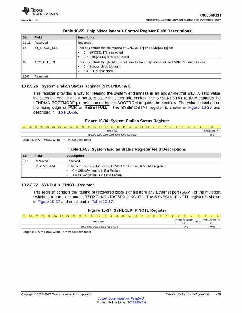
229
TCI6636K2Hwww.ti.com SPRS835H –FEBRUARY 2012–REVISED OCTOBER 2017
Submit Documentation FeedbackProduct Folder Links: TCI6636K2H
Device Boot and ConfigurationCopyright © 2012–2017, Texas Instruments Incorporated
Table 10-55. Chip Miscellaneous Control Register Field DescriptionsBit Field Description31-15 Reserved Reserved.14 IO_TRACE_SEL This bit controls the pin muxing of GPIO[31:17] and EMU[33:19] pin
• 0 = GPIO[31:17] is selected• 1 = EMU[33:19] pins is selected
13 ARM_PLL_EN This bit controls the glitchfree clock mux between bypass clock and ARM PLL output clock• 0 = Bypass clock (default)• 1 = PLL output clock
12-0 Reserved
10.2.3.26 System Endian Status Register (SYSENDSTAT)
This register provides a way for reading the system endianness in an endian-neutral way. A zero valueindicates big endian and a nonzero value indicates little endian. The SYSENDSTAT register captures theLENDIAN BOOTMODE pin and is used by the BOOTROM to guide the bootflow. The value is latched onthe rising edge of POR or RESETFULL . The SYSENDSTAT register is shown in Figure 10-36 anddescribed in Table 10-56.
Figure 10-36. System Endian Status Register31 30 29 28 27 26 25 24 23 22 21 20 19 18 17 16 15 14 13 12 11 10 9 8 7 6 5 4 3 2 1 0
Reserved SYSENDSTAT
R-0000 0000 0000 0000 0000 0000 0000 000 R-0
Legend: RW = Read/Write; -n = value after reset
Table 10-56. System Endian Status Register Field DescriptionsBit Field Description31-1 Reserved Reserved0 SYSENDSTAT Reflects the same value as the LENDIAN bit in the DEVSTAT register.
• 0 = C66x/System is in Big Endian• 1 = C66x/System is in Little Endian
10.2.3.27 SYNECLK_PINCTL Register
This register controls the routing of recovered clock signals from any Ethernet port (SGMII of the multiportswitches) to the clock output TSRXCLKOUT0/TSRXCLKOUT1. The SYNECLK_PINCTL register is shownin Figure 10-37 and described in Table 10-57.
Figure 10-37. SYNECLK_PINCTL Register31 30 29 28 27 26 25 24 23 22 21 20 19 18 17 16 15 14 13 12 11 10 9 8 7 6 5 4 3 2 1 0
Reserved TSRXCLKOUT1SEL Rsvd TSRXCLKOUT0
SEL
R-0000 0000 0000 0000 0000 0000 0 RW-0 RW-0
Legend: RW = Read/Write; -n = value after reset

230
TCI6636K2HSPRS835H –FEBRUARY 2012–REVISED OCTOBER 2017 www.ti.com
Submit Documentation FeedbackProduct Folder Links: TCI6636K2H
Device Boot and Configuration Copyright © 2012–2017, Texas Instruments Incorporated
Table 10-57. SYNECLK_PINCTL Register Field DescriptionsBit Field Description31-7 Reserved6-4 TSRXCLKOUT1SEL • 000 = SGMII Lane 0 rxbclk
• 001 = SGMII Lane 1 rxbclk• 010 = SGMII Lane 2 rxbclk• 011 = SGMII Lane 3 rxbclk• 100 = Reserved. Do not write.• 101 = Reserved. Do not write.• 110 = Reserved. Do not write.• 111 = Reserved. Do not write.
3 Reserved2-0 TSRXCLKOUT0SEL • 000 = SGMII Lane 0 rxbclk
• 001 = SGMII Lane 1 rxbclk• 010 = SGMII Lane 2 rxbclk• 011 = SGMII Lane 3 rxbclk• 100 = Reserved. Do not write.• 101 = Reserved. Do not write.• 110 = Reserved. Do not write.• 111 = Reserved. Do not write.
10.2.3.28 USB PHY Control (USB_PHY_CTLx) Registers
The USB PHY Control (USB_PHY_CTLx) registers are shown in Figure 10-38, Figure 10-39, Figure 10-40, Figure 10-41, Figure 10-42, and Figure 10-43 and described in Table 10-58, Table 10-59, Table 10-60,Table 10-61, Figure 10-42, and Table 10-63.
Figure 10-38. USB_PHY_CTL0 Register31 30 29 28 27 26 25 24 23 22 21 20 19 18 17 16
Reserved
R-0
15 14 13 12 11 10 9 8 7 6 5 4 3 2 1 0
ReservedPHY_
RTUNE_ACK
PHY_RTUNE_
REQRsvd PHY_TC_
VATESTENB
PHY_TC_TEST_
POWERDOWN_
SSP
PHY_TC_TEST_
POWERDOWN_
HSP
PHY_TC_LOOP
BACKENBRsvd
UTMI_VBUS
VLDEXT
UTMI_TXBITSTUFF
ENH
UTMI_TXBITSTUFF
EN
R-0 R-0 R/W-0 R-0 R/W-00 R/W-0 R/W-0 R/W-0 R-0 R/W-0 R/W-0 R/W-0
Legend: R = Read only; W = Write only; -n = value after reset
Table 10-58. USB_PHY_CTL0 Register Field DescriptionsBit Field Description31-12 Reserved Reserved11 PHY_RTUNE_ACK The PHY uses an external resistor to calibrate the termination impedances of the PHY's high-
speed inputs and outputs.
The resistor is shared between the USB2.0 high-speed outputs and the Super-speed I/O. Eachtime the PHY is taken out of a reset, a termination calibration is performed. For SS link, thecalibration can also be requested externally by asserting the PHY_RTUNE_REQ. When thecalibration is complete, the PHY_RTUNE_ACK transitions low.
A resistor calibration on the SS link cannot be performed while the link is operational10 PHY_RTUNE_REQ See PHY_RTUNE_ACK.9 Reserved Reserved

231
TCI6636K2Hwww.ti.com SPRS835H –FEBRUARY 2012–REVISED OCTOBER 2017
Submit Documentation FeedbackProduct Folder Links: TCI6636K2H
Device Boot and ConfigurationCopyright © 2012–2017, Texas Instruments Incorporated
Table 10-58. USB_PHY_CTL0 Register Field Descriptions (continued)Bit Field Description8-7 PHY_TC_VATESTENB Analog Test Pin Select.
Enables analog test voltages to be placed on the ID pin.• 11 = Invalid setting.• 10 = Invalid setting.• 01 = Analog test voltages can be viewed or applied on ID.• 00 = Analog test voltages cannot be viewed or applied on ID.
6 PHY_TC_TEST_POWERDOWN_SSP
SS Function Circuits Power-Down Control.
Powers down all SS function circuitry in the PHY for IDDQ testing.5 PHY_TC_TEST_POWERDOWN
_HSPHS Function Circuits Power-Down Control
Powers down all HS function circuitry in the PHY for IDDQ testing.4 PHY_TC_LOOPBACKENB Loop-back Test Enable
Places the USB3.0 PHY in HS Loop-back mode, which concurrently enables the HS receiveand transmit logic.• 1 = During HS data transmission, the HS receive logic is enabled.• 0 = During HS data transmission, the HS receive logic is disabled.
3 Reserved • Reserved2 UTMI_VBUSVLDEXT External VBUS Valid Indicator
Function: Valid in Device mode and only when the VBUSVLDEXTSEL signal is set to 1'b1.VBUSVLDEXT indicates whether the VBUS signal on the USB cable is valid. In addition,VBUSVLDEXT enables the pull-up resistor on the D+ line.• 1 = VBUS signal is valid, and the pull-up resistor on D+ is enabled.• 0 = VBUS signal is not valid, and the pull-up resistor on D+ is disabled.
1 UTMI_TXBITSTUFFENH High-byte Transmit Bit-Stuffing Enable
Function: controls bit stuffing on DATAINH[7:0] when OPMODE[1:0]=11b.• 1 = Bit stuffing is enabled.• 0 = Bit stuffing is disabled.
0 UTMI_TXBITSTUFFEN Low-byte Transmit Bit-Stuffing Enable
Function: controls bit stuffing on DATAIN[7:0] when OPMODE[1:0]=11b.• 1 = Bit stuffing is enabled.• 0 = Bit stuffing is disabled.
Figure 10-39. USB_PHY_CTL1 Register31 30 29 28 27 26 25 24 23 22 21 20 19 18 17 16
Reserved
R-0
15 14 13 12 11 10 9 8 7 6 5 4 3 2 1 0
ReservedPIPE_REF_CLKREQ
_N
PIPE_TX2RX_LOOP
BK
PIPE_EXT_PCLK_
REQ
PIPE_ALT_CLK_
SEL
PIPE_ALT_CLK_REQ
PIPE_ALT_CLK_EN
R-0 R-0 R/W-0 R/W-0 R/W-0 R-0 R/W-0
Legend: R = Read only; R/W = Read/Write, -n = value after reset
Table 10-59. USB_PHY_CTL1 Register Field DescriptionsBit Field Description31-6 Reserved Reserved5 PIPE_REF_CLKREQ_N Reference Clock Removal Acknowledge.
When the pipeP_power-down control into the PHY turns off the MPLL in the P3 state,PIPE_REF_CLKREQ_N is asserted after the PLL is stable and the reference clock can beremoved.

232
TCI6636K2HSPRS835H –FEBRUARY 2012–REVISED OCTOBER 2017 www.ti.com
Submit Documentation FeedbackProduct Folder Links: TCI6636K2H
Device Boot and Configuration Copyright © 2012–2017, Texas Instruments Incorporated
Table 10-59. USB_PHY_CTL1 Register Field Descriptions (continued)Bit Field Description4 PIPE_TX2RX_LOOPBK Loop-back.
When this signal is asserted, data from the transmit predriver is looped back to the receiverslicers. LOS is bypassed and based on the tx_en input so that rx_los=!tx_data_en.
3 PIPE_EXT_PCLK_REQ External PIPE Clock Enable Request.
When asserted, this signal enables the pipeP_pclk output regardless of power state (alongwith the associated increase in power consumption).
2 PIPE_ALT_CLK_SEL Alternate Clock Source Select.
Selects the alternate clock sources instead of the internal MPLL outputs for the PCS clocks.• 1 = Uses alternate clocks.• 0 = Users internal MPLL clocks.
Change only during a reset.1 PIPE_ALT_CLK_REQ Alternate Clock Source Request.
Indicates that the alternate clocks are needed by the slave PCS (that is, to boot the masterMPLL). Connect to the alt_clk_en on the master.
0 PIPE_ALT_CLK_EN Alternate Clock Enable.
Enables the ref_pcs_clk and ref_pipe_pclk output clocks (if necessary, powers up the MPLL).
Figure 10-40. USB_PHY_CTL2 Register31 30 29 28 27 26 25 24 23 22 21 20 19 18 17 16
Reserved PHY_PC_LOS_BIAS PHY_PC_TXVREFTUNE PHY_PC_TXRISETUNE
PHY_PC_TXRESTUNE
PHY_PC_TX
PREEMPPULSE
TUNE
PHY_PC_TXPREEMPAMPTUNE
R-0 R/W-101 R/W-1000 R/W-01 R/W-01 R/W-0 R/W-00
15 14 13 12 11 10 9 8 7 6 5 4 3 2 1 0
PHY_PC_TXHSXVTUNE PHY_PC_TXFSLSTUNE PHY_PC_SQRXTUNE PHY_PC_OTGTUNE Rsvd PHY_PC_
COMPDISTUNE
R/W-11 R/W-0011 R/W-011 R/W-100 R-0 R/W-100
Legend: R = Read only; R/W = Read/Write, -n = value after reset
Table 10-60. USB_PHY_CTL2 Register Field DescriptionsBit Field Description31-30 Reserved Reserved29-27 PHY_PC_LOS_BIAS Loss-of-Signal Detector Threshold Level Control.
Sets the LOS detection threshold level.• +1 = results in a +15 mVp incremental change in the LOS threshold.• –1 = results in a –15 mVp incremental change in the LOS threshold.
Note: the 000b setting is reserved and must not be used.26-23 PHY_PC_TXVREFTUNE HS DC Voltage Level Adjustment.
Adjusts the high-speed DC level voltage.• +1 = results in a +1.25% incremental change in high-speed DC voltage level.• –1 = results in a –1.25% incremental change in high-speed DC voltage level.
22-21 PHY_PC_TXRISETUNE HS Transmitter Rise/Fall TIme Adjustment.
Adjusts the rise/fall times of the high-speed waveform.• +1 = results in a –4% incremental change in the HS rise/fall time.• –1 = results in a +4% incremental change in the HS rise/fall time.
20-19 PHY_PC_TXRESTUNE USB Source Impedance Adjustment.
Some applications require additional devices to be added on the USB, such as a seriesswitch, which can add significant series resistance. This bus adjusts the driver sourceimpedance to compensate for added series resistance on the USB.

233
TCI6636K2Hwww.ti.com SPRS835H –FEBRUARY 2012–REVISED OCTOBER 2017
Submit Documentation FeedbackProduct Folder Links: TCI6636K2H
Device Boot and ConfigurationCopyright © 2012–2017, Texas Instruments Incorporated
Table 10-60. USB_PHY_CTL2 Register Field Descriptions (continued)Bit Field Description18 PHY_PC_
TXPREEMPPULSETUNEHS Transmitter Pre-Emphasis Duration Control.
Controls the duration for which the HS pre-emphasis current is sourced onto DP or DM. It isdefined in terms of unit amounts. One unit of pre-emphasis duration is approximately 580 psand is defined as 1x pre-emphasis duration. This signal valid only if eithertxpreempamptune[1] or txpreempamptune[0] is set to 1.• 1 = 1x, short pre-emphasis current duration.• 0 = 2x, long pre-emphasis current duration.
17-16 PHY_PC_TXPREEMPAMPTUNE HS Transmitter Pre-Emphasis Current Control.
Controls the amount of current sourced to DP and DM after a J-to-K or K-to-J transition.
The HS Transmitter pre-emphasis current is defined in terms of unit amounts. One unitamount is approximately 600 µA and is defined as 1x pre-emphasis current.• 11 = 3x pre-emphasis current.• 10 = 2x pre-emphasis current.• 01 = 1x pre-emphasis current.• 00 = HS Transmitter pre-emphasis is disabled.
15-14 PHY_PC_TXHSXVTUNE Transmitter High-Speed Crossover Adjustment.
Adjusts the voltage at which the DP and DM signals cross while transmitting in HS mode.• 11 = Default setting.• 10 = +15 mV• 01 = –15 mV• 00 = Reserved
13-10 PHY_PC_TXFSLSTUNE FS/LS Source Impedance Adjustment.
Adjusts the low- and full-speed single-ended source impedance while driving high.
This parameter control is encoded in thermometer code.• +1 = results in a –2.5% incremental change in threshold voltage level.• –1 = results in a +2.5% incremental change in threshold voltage level.
Any nonthermometer code setting (that is 1001) is not supported and reserved.9-7 PHY_PC_SQRXTUNE Squelch Threshold Adjustment.
Adjusts the voltage level for the threshold used to detect valid high-speed data.• +1 = results in a –5% incremental change in threshold voltage level.• –1 = results in a +5% incremental change in threshold voltage level.
6-4 PHY_PC_OTGTUNE VBUS Valid Threshold Adjustment.
Adjusts the voltage level for the VBUS valid threshold.• +1 = results in a +1.5% incremental change in threshold voltage level.• –1 = results in a –1.5% incremental change in threshold voltage level.
3 Reserved Reserved2-0 PHY_PC_COMPDISTUNE Disconnect Threshold Adjustment.
Adjusts the voltage level for the threshold used to detect a disconnect event at the host.• +1 = results in a +1.5% incremental change in the threshold voltage level.• –1 = results in a –1.5% incremental change in the threshold voltage level.
Figure 10-41. USB_PHY_CTL3 Register31 30 29 28 27 26 25 24 23 22 21 20 19 18 17 16
Reserved PHY_PC_PCS_TX_SWING_FULL PHY_PC_PCS_TX_DEEMPH_6DB Rsvd
R-0 R/W-1111000 R/W-100000 R-0
15 14 13 12 11 10 9 8 7 6 5 4 3 2 1 0
Reserved PHY_PC_PCS_TX_DEEMPH_3P5DB PHY_PC_LOS_LEVEL
R-0 R/W-010101 R/W-01001
Legend: R = Read only; R/W = Read/Write, -n = value after reset

234
TCI6636K2HSPRS835H –FEBRUARY 2012–REVISED OCTOBER 2017 www.ti.com
Submit Documentation FeedbackProduct Folder Links: TCI6636K2H
Device Boot and Configuration Copyright © 2012–2017, Texas Instruments Incorporated
Table 10-61. USB_PHY_CTL3 Register Field DescriptionsBit Field Description31-30 Reserved Reserved29-23 PHY_PC_PCS_TX_SWING_
FULLTx Amplitude (Full Swing Mode).
Sets the launch amplitude of the transmitter. It can be used to tune Rx eye for compliance.22-17 PHY_PC_PCS_TX_DEEMPH_
6DBTx De-Emphasis at 6 dB.
Sets the Tx driver de-emphasis value when pipeP_tx_deemph[1:0] is set to 10b (according tothe PIPE3 specification). This bus is provided for completeness and as a second potentiallaunch amplitude.
16-11 Reserved Reserved10-5 PHY_PC_PCS_TX_DEEMPH_
3P5DBTx De-Emphasis at 3.5 dB.
Sets the Tx driver de-emphasis value when pipeP_tx_deemph[1:0] is set to 10b (according tothe PIPE3 specification). Can be used for Rx eye compliance.
4-0 PHY_PC_LOS_LEVEL Loss-of-Signal Detector Sensitivity Level Control.
Sets the LOS detection threshold level. This signal must be set to 0x9.
Figure 10-42. USB_PHY_CTL4 Register31 30 29 28 27 26 25 24 23 22 21 20 19 18 17 16
PHY_SSC_EN
PHY_REF_USE_PAD
PHY_REF_SSP_EN
PHY_MPLL_
REFSSC_CLK_EN
PHY_FSEL PHY_RETENABLEN PHY_REFCLKSEL
PHY_COMMON
ONNRsvd
PHY_OTG_VBUSVLDEXTSEL
R/W-1 R/W-0 R/W-0 R/W-0 R/W-100111 R/W-1 R/W-10 R/W-0 R-0 R/W-0
15 14 13 12 11 10 9 8 7 6 5 4 3 2 1 0
PHY_OTG_ OTG
DISABLEPHY_PC_TX_VBOOST_LVL PHY_PC_LANE0_TX_TERM_
OFFSET Reserved
R/W-1 R/W-100 R/W-00000 R-0
Legend: R = Read only; R/W = Read/Write, -n = value after reset
Table 10-62. USB_PHY_CTL4 Register Field DescriptionsBit Field Description31 PHY_SSC_EN Spread Spectrum Enable.
Enables spread spectrum clock production (0.5% down-spread at ~31.5 KHz) in the USB3.0PHY. If the reference clock already has spread spectrum applied, ssc_en must be deasserted.
30 PHY_REF_USE_PAD Select Reference Clock Connected to ref_pad_clk_{p,m}.
When asserted, selects the external ref_pad_clk_{p,m} inputs as the reference clock source.When deasserted, ref_alt_clk_{p,m} are selected for an on-chip reference clock source.
29 PHY_REF_SSP_EN Reference Clock Enables for SS function.
Enables the reference clock to the prescaler. The ref_ssp_en signal must remain deasserteduntil the reference clock is running at the appropriate frequency, at which point ref_ssp_en canbe asserted. For lower power states, ref_ssp_en can also be de asserted.
28 PHY_MPLL_REFSSC_CLK_EN Double-Word Clock Enable.
Enables/disables the mpll_refssc_clk signal. To prevent clock glitch, it must be changed whenthe PHY is inactive.
27-22 PHY_FSEL Frequency Selection.
Selects the reference clock frequency used for both SS and HS operations. The value for fselcombined with the other clock and enable signals will determine the clock frequency used forSS and HS operations and if a shared or separate reference clock will be used.
21 PHY_RETENABLEN Lowered Digital Supply Indicator.
Indicates that the vp digital power supply has been lowered in Suspend mode. This signalmust be deasserted before the digital power supply is lowered.• 1 = Normal operating mode.• 0 = The analog blocks are powered down.

235
TCI6636K2Hwww.ti.com SPRS835H –FEBRUARY 2012–REVISED OCTOBER 2017
Submit Documentation FeedbackProduct Folder Links: TCI6636K2H
Device Boot and ConfigurationCopyright © 2012–2017, Texas Instruments Incorporated
Table 10-62. USB_PHY_CTL4 Register Field Descriptions (continued)Bit Field Description20-19 PHY_REFCLKSEL Reference Clock Select for PLL Block.
Selects reference clock source for the HS PLL block.• 11 = HS PLL uses EXTREFCLK as reference.• 10 = HS PLL uses either ref_pad_clk_{p,m} or ref_alt_clk_{p,m} as reference.• x0 = Reserved.
18 PHY_COMMONONN Common Block Power-Down Control.
Controls the power-down signals in the HS Bias and PLL blocks when the USB3.0 PHY is inSuspend or Sleep mode.• 1 = In Suspend or Sleep mode, the HS Bias and PLL blocks are powered down.• 0 = In Suspend or Sleep mode, the HS Bias and PLL blocks remain powered and continue
to draw current.17 Reserved Reserved16 PHY_OTG_VBUSVLDEXTSEL External VBUS Valid Select.
Selects the VBUSVLDEXT input or the internal Session Valid comparator to indicate when theVBUS signal on the USB cable is valid.• 1 = VBUSVLDEXT input is used.• 0 = Internal Session Valid comparator is used.
15 PHY_OTG_OTGDISABLE OTG Block Disable.
Powers down the OTG block, which disables the VBUS Valid and Session End comparators.The Session Valid comparator (the output of which is used to enable the pull-up resistor on DPin Device mode) is always on irrespective of the state of otgdisable. If the application does notuse the OTG function, setting this signal to high to save power.• 1 = OTG block is powered down.• 0 = OTG block is powered up.
14-12 PHY_PC_TX_VBOOST_LVL Tx Voltage Boost Level.
Sets the boosted transmit launch amplitude (mVppd).
The default setting is intended to set the launch amplitude to approximately 1,008mVppd.• +1 = results in a +156 mVppd change in the Tx launch amplitude.• –1 = results in a –156 mVppd change in the Tx launch amplitude.
11-7 PHY_PC_LANE0_TX_TERM_OFFSET
Transmitter Termination Offset.
Enables adjusting the transmitter termination value from the default value of 60 Ω.6-0 Reserved Reserved
Figure 10-43. USB_PHY_CTL5 Register31 30 29 28 27 26 25 24 23 22 21 20 19 18 17 16
Reserved PHY_REF_CLKDIV2 PHY_MPLL_MULTIPLIER[6:0]
R-0 R/W-0 R/W +0011001
15 14 13 12 11 10 9 8 7 6 5 4 3 2 1 0
PHY_MPLL_MULTIPLIER[6:0] PHY_SSC_REF_CLK_SEL Rsvd PHY_SSC_RANGE
R/W +0011001 R/W-000000000 R-0 R/W-000
Legend: R = Read only; R/W = Read/Write, -n = value after reset
Table 10-63. USB_PHY_CTL5 Register Field DescriptionsBit Field Description31-21 Reserved Reserved20 PHY_REF_CLKDIV2 Input Reference Clock Divider Control.
If the input reference clock frequency is greater than 100 MHz, this signal must be asserted.The reference clock frequency is then divided by 2 to keep it in the range required by theMPLL.
When this input is asserted, the ref_ana_usb2_clk (if used) frequency will be the referenceclock frequency divided by 4.

236
TCI6636K2HSPRS835H –FEBRUARY 2012–REVISED OCTOBER 2017 www.ti.com
Submit Documentation FeedbackProduct Folder Links: TCI6636K2H
Device Boot and Configuration Copyright © 2012–2017, Texas Instruments Incorporated
Table 10-63. USB_PHY_CTL5 Register Field Descriptions (continued)Bit Field Description19-13 PHY_MPLL_MULTIPLIER[6:0] MPLL Frequency Multiplier Control.
Multiplies the reference clock to a frequency suitable for intended operating speed.12-4 PHY_SSC_REF_CLK_SEL Spread Spectrum Reference Clock Shifting.
Enables nonstandard oscillator frequencies to generate targeted MPLL output rates. Inputcorresponds to frequency-synthesis coefficient.• . ssc_ref_clk_sel[8:6] = modulous – 1• . ssc_ref_clk_sel[5:0] = 2's complement push amount.
3 Reserved Reserved2-0 PHY_SSC_RANGE Spread Spectrum Clock Range.
Selects the range of spread spectrum modulation when ssc_en is asserted and the PHY isspreading the high-speed transmit clocks. Applies a fixed offset to the phase accumulator.

237
TCI6636K2Hwww.ti.com SPRS835H –FEBRUARY 2012–REVISED OCTOBER 2017
Submit Documentation FeedbackProduct Folder Links: TCI6636K2H
TCI6636K2H Peripheral InformationCopyright © 2012–2017, Texas Instruments Incorporated
11 TCI6636K2H Peripheral Information
This chapter covers the various peripherals on the TCI6636K2H device. Peripheral-specific information,timing diagrams, electrical specifications, and register memory maps are described in this chapter.
11.1 Recommended Clock and Control Signal Transition BehaviorAll clocks and control signals must transition between VIH and VIL (or between VIL and VIH) in a monotonicmanner.
11.2 Power SuppliesThe following sections describe the proper power-supply sequencing and timing needed to properly poweron the TCI6636K2H. The various power supply rails and their primary functions are listed in Table 11-1.
Table 11-1. Power Supply Rails on the TCI6636K2H
Name Primary Function Voltage NotesAVDDAx Core PLL, DDR3 DLL supply voltage 1.8 V Core PLL, DDR3 DLL supplyCVDD SmartReflex DSP core supply voltage 0.8 – 1.1 V DSP variable core supplyCVDD1 DSP core fixed supply voltage 0.95 V DSP Core fixed supplyCVDDT1 ARM core fixed supply voltage 0.95 V ARM core fixed supplyDVDD15 DDR3A, DDR3B I/O power supply
voltage1.35 V / 1.5 V DDR3A, DDR3B I/O power supply
DVDD18 1.8-V I/O power supply voltage 1.8 V 1.8-V I/O power supplyDVDD33 USB 3.3-V IO supply 3.3 V USB high voltage supplyVDDAHV SerDes I/O power supply voltage 1.8 V SerDes I/O power supplyVDDALV SerDes analog power supply voltage 0.85 V SerDes analog supplyVDDUSB USB LV PHY power supply voltage 0.85 V USB LV PHY supplyVP, VPTX Filtered 0.85-V supply voltage 0.85 V Filtered 0.85-V USB supplyVSS Ground GND Ground
11.2.1 Power-Up SequencingThis section defines the requirements for a power-up sequencing from a power-on reset condition. Thereare two acceptable power sequences for the device.
The first sequence stipulates the core voltages starting before the IO voltages as shown below.1. CVDD2. CVDD1, CVDDT1, VDDAHV, AVDDAx, DVDD183. DVDD154. VDDALV, VDDUSB, VP, VPTX5. DVDD33
The second sequence provides compatibility with other TI processors with the IO voltage starting beforethe core voltages as shown below.1. VDDAHV, AVDDAx, DVDD182. CVDD3. CVDD1, CVDDT14. DVDD155. VDDALV, VDDUSB, VP, VPTX6. DVDD33

238
TCI6636K2HSPRS835H –FEBRUARY 2012–REVISED OCTOBER 2017 www.ti.com
Submit Documentation FeedbackProduct Folder Links: TCI6636K2H
TCI6636K2H Peripheral Information Copyright © 2012–2017, Texas Instruments Incorporated
The clock input buffers for SYSCLK, ARMCLK, ALTCORECLK, DDR3ACLK, DDR3BCLK, PASSCLK, andSRIOSGMIICLK use CVDD as a supply voltage. These clock inputs are not failsafe and must be held in ahigh-impedance state until CVDD is at a valid voltage level. Driving these clock inputs high before CVDDis valid could cause damage to the device. Once CVDD is valid, it is acceptable that the P and N legs ofthese clocks may be held in a static state (either high and low or low and high) until a valid clockfrequency is needed at that input. To avoid internal oscillation, the clock inputs should be removed fromthe high impedance state shortly after CVDD is present.
If a clock input is not used, it must be held in a static state. To accomplish this, the N leg should be pulledto ground through a 1-kΩ resistor. The P leg should be tied to CVDD to ensure it will not have any voltagepresent until CVDD is active. Connections to the IO cells powered by DVDD18 and DVDD15 are notfailsafe and should not be driven high before these voltages are active. Driving these IO cells high beforeDVDD18 or DVDD15 are valid could cause damage to the device.
The device initialization is divided into two phases. The first phase consists of the time period from theactivation of the first power supply until the point at which all supplies are active and at a valid voltagelevel. Either of the sequencing scenarios described above can be implemented during this phase. Thefigures below show both the core-before-IO voltage sequence and the IO-before-core voltage sequence.POR must be held low for the entire power stabilization phase.
This is followed by the device initialization phase. The rising edge of POR followed by the rising edge ofRESETFULL triggers the end of the initialization phase, but both must be inactive for the initialization tocomplete. POR must always go inactive before RESETFULL goes inactive as described below. SYSCLK1in the following section refers to the clock that is used by the CorePacs. See Figure 11-7 for more details.
11.2.1.1 Core-Before-IO Power Sequencing
The details of the Core-before-IO power sequencing are defined in Table 11-2. Figure 11-1 shows powersequencing and reset control of the TCI6636K2H. POR may be removed after the power has been stablefor the required 100 µsec. RESETFULL must be held low for a period (see item 9 in Figure 11-1) after therising edge of POR, but may be held low for longer periods if necessary. The configuration bits sharedwith the GPIO pins will be latched on the rising edge of RESETFULL and must meet the setup and holdtimes specified. SYSCLK1 must always be active before POR can be removed.
NOTETI recommends a maximum of 80 ms between one power rail being valid and the next powerrail in the sequence starting to ramp.
Table 11-2. Core-Before-IO Power Sequencing
ITEM SYSTEM STATE1 Begin Power Stabilization Phase
• CVDD (core AVS) ramps up.• POR must be held low through the power stabilization phase. Because POR is low, all the core logic that has asynchronous
reset (created from POR) is put into the reset state.• Each supply must ramp monotonically and must reach a stable valid level in 20 ms or less.
2a • CVDD1 and CVDDT1 (core constant) ramps at the same time or within 80 ms of CVDD. Although ramping CVDD1simultaneously with CVDD is permitted, the voltage for CVDD1 must never exceed CVDD until after CVDD has reached avalid voltage.
• The purpose of ramping up the core supplies close to each other is to reduce crowbar current. CVDD1 should trail CVDD asthis will ensure that the Word Lines (WLs) in the memories are turned off and there is no current through the memory bitcells. If, however, CVDD1 (core constant) ramps up before CVDD (core AVS), then the worst-case current could be on theorder of twice the specified draw of CVDD1.
• Each supply must ramp monotonically and must reach a stable valid level in 20 ms or less.• The timing for CVDD1 is based on CVDD valid. CVDD1 and DVDD18/ADDAVH/AVDDAx may be enabled at the same time
but do not need to ramp simultaneously. CVDD1 may be valid before or after DVDD18/ADDAVH/AVDDAx are valid, as longas the timing above is met.
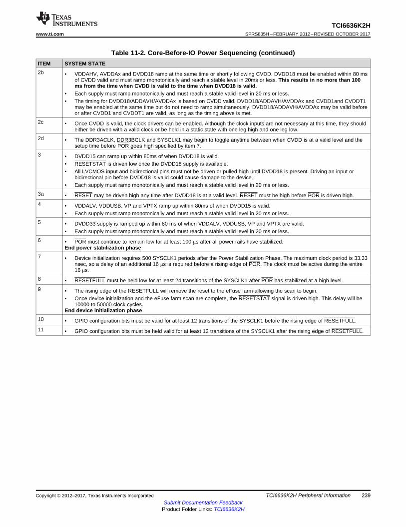
239
TCI6636K2Hwww.ti.com SPRS835H –FEBRUARY 2012–REVISED OCTOBER 2017
Submit Documentation FeedbackProduct Folder Links: TCI6636K2H
TCI6636K2H Peripheral InformationCopyright © 2012–2017, Texas Instruments Incorporated
Table 11-2. Core-Before-IO Power Sequencing (continued)ITEM SYSTEM STATE2b • VDDAHV, AVDDAx and DVDD18 ramp at the same time or shortly following CVDD. DVDD18 must be enabled within 80 ms
of CVDD valid and must ramp monotonically and reach a stable level in 20ms or less. This results in no more than 100ms from the time when CVDD is valid to the time when DVDD18 is valid.
• Each supply must ramp monotonically and must reach a stable valid level in 20 ms or less.• The timing for DVDD18/ADDAVH/AVDDAx is based on CVDD valid. DVDD18/ADDAVH/AVDDAx and CVDD1and CVDDT1
may be enabled at the same time but do not need to ramp simultaneously. DVDD18/ADDAVH/AVDDAx may be valid beforeor after CVDD1 and CVDDT1 are valid, as long as the timing above is met.
2c • Once CVDD is valid, the clock drivers can be enabled. Although the clock inputs are not necessary at this time, they shouldeither be driven with a valid clock or be held in a static state with one leg high and one leg low.
2d • The DDR3ACLK, DDR3BCLK and SYSCLK1 may begin to toggle anytime between when CVDD is at a valid level and thesetup time before POR goes high specified by item 7.
3 • DVDD15 can ramp up within 80ms of when DVDD18 is valid.• RESETSTAT is driven low once the DVDD18 supply is available.• All LVCMOS input and bidirectional pins must not be driven or pulled high until DVDD18 is present. Driving an input or
bidirectional pin before DVDD18 is valid could cause damage to the device.• Each supply must ramp monotonically and must reach a stable valid level in 20 ms or less.
3a • RESET may be driven high any time after DVDD18 is at a valid level. RESET must be high before POR is driven high.4 • VDDALV, VDDUSB, VP and VPTX ramp up within 80ms of when DVDD15 is valid.
• Each supply must ramp monotonically and must reach a stable valid level in 20 ms or less.5 • DVDD33 supply is ramped up within 80 ms of when VDDALV, VDDUSB, VP and VPTX are valid.
• Each supply must ramp monotonically and must reach a stable valid level in 20 ms or less.6 • POR must continue to remain low for at least 100 μs after all power rails have stabilized.
End power stabilization phase7 • Device initialization requires 500 SYSCLK1 periods after the Power Stabilization Phase. The maximum clock period is 33.33
nsec, so a delay of an additional 16 μs is required before a rising edge of POR. The clock must be active during the entire16 μs.
8 • RESETFULL must be held low for at least 24 transitions of the SYSCLK1 after POR has stabilized at a high level.9 • The rising edge of the RESETFULL will remove the reset to the eFuse farm allowing the scan to begin.
• Once device initialization and the eFuse farm scan are complete, the RESETSTAT signal is driven high. This delay will be10000 to 50000 clock cycles.
End device initialization phase10 • GPIO configuration bits must be valid for at least 12 transitions of the SYSCLK1 before the rising edge of RESETFULL.11 • GPIO configuration bits must be held valid for at least 12 transitions of the SYSCLK1 after the rising edge of RESETFULL.

RESET
RESETFULL
POR
CVDD
CVDD1CVDDT1
DVDD15
DVDD33
SYSCLK1
DDRCLKOUT
RESETSTAT
Power Stabilization Phase Device Initialization Phase
3a
2a
2d
ConfigurationInputs
9
8
11
1
VDDALVVDDUSBVP, VPTX
2bVDDAHVAVDDAxDVDD18
3
7
2c
10
1
2
3
4
5
6
4
5
240
TCI6636K2HSPRS835H –FEBRUARY 2012–REVISED OCTOBER 2017 www.ti.com
Submit Documentation FeedbackProduct Folder Links: TCI6636K2H
TCI6636K2H Peripheral Information Copyright © 2012–2017, Texas Instruments Incorporated
Figure 11-1. Core-Before-IO Power Sequencing

241
TCI6636K2Hwww.ti.com SPRS835H –FEBRUARY 2012–REVISED OCTOBER 2017
Submit Documentation FeedbackProduct Folder Links: TCI6636K2H
TCI6636K2H Peripheral InformationCopyright © 2012–2017, Texas Instruments Incorporated
11.2.1.2 IO-Before-Core Power Sequencing
The timing diagram for IO-before-core power sequencing is shown in Figure 11-2 and defined in Table 11-3.
NOTETI recommends a maximum of 100 ms between one power rail being valid, and the nextpower rail in the sequence starting to ramp.
Table 11-3. IO-Before-Core Power Sequencing
ITEM SYSTEM STATE1 Begin Power Stabilization Phase
• VDDAHV, AVDDAx and DVDD18 ramp up.• POR must be held low through the power stabilization phase. Because POR is low, all the core logic that has asynchronous
reset (created from POR ) is put into the reset state.• Each supply must ramp monotonically and must reach a stable valid level in 20 ms or less.
2 • CVDD (core AVS) ramps within 80 ms from the time ADDAHV, AVDDAx and DVDD18 are valid.• Each supply must ramp monotonically and must reach a stable valid level in 20 ms or less.
2a • RESET may be driven high any time after DVDD18 is at a valid level. must be high before POR is driven high.3 • CVDD1 and CVDDT1 (core constant) ramp at the same time or within 80 ms following CVDD. Although ramping CVDD1and
CVDDT1 simultaneously with CVDD is permitted, the voltage for CVDD1 and CVDDT1 must never exceed CVDD untilafter CVDD has reached a valid voltage.
• The purpose of ramping up the core supplies close to each other is to reduce crowbar current. CVDD1 and CVDDT1 shouldtrail CVDD as this will ensure that the Word Lines (WLs) in the memories are turned off and there is no current through thememory bit cells. If, however, CVDD1 and CVDDT1 (core constant) ramp up before CVDD (core AVS), then the worst-casecurrent could be on the order of twice the specified draw of CVDD1 and CVDDT1.
• Each supply must ramp monotonically and must reach a stable valid level in 20 ms or less.3a • Once CVDD is valid, the clock drivers can be enabled. Although the clock inputs are not necessary at this time, they should
either be driven with a valid clock or held in a static state.3b • The DDR3ACLK, DDR3BCLK and SYSCLK1 may begin to toggle anytime between when CVDD is at a valid level and the
setup time before POR goes high specified by item 8.4 • DVDD15 can ramp up within 80 ms of when CVDD1 is valid.
• RESETSTAT is driven low once the DVDD18 supply is available.• All LVCMOS input and bidirectional pins must not be driven or pulled high until DVDD18 is present. Driving an input or
bidirectional pin before DVDD18 is valid could cause damage to the device.• Each supply must ramp monotonically and must reach a stable valid level in 20 ms or less.
5 • VDDALV, VDDUSB, VP and VPTX should ramp up within 80 ms of when DVDD15 is valid.• Each supply must ramp monotonically and must reach a stable valid level in 20 ms or less.
6 • DVDD33 supply is ramped up within 80 ms of when VDDALV, VDDUSB, VP and VPTX are valid.• Each supply must ramp monotonically and must reach a stable valid level in 20 ms or less.
7 • POR must continue to remain low for at least 100 μs after all power rails have stabilized.End power stabilization phase
8 • Device initialization requires 500 SYSCLK1 periods after the Power Stabilization Phase. The maximum clock period is 33.33nsec, so a delay of an additional 16 μs is required before a rising edge of POR. The clock must be active during the entire16 μs.
9 • RESETFULL must be held low for at least 24 transitions of the SYSCLK1 after POR has stabilized at a high level.10 • The rising edge of the RESETFULL will remove the reset to the efuse farm allowing the scan to begin.
• Once device initialization and the efuse farm scan are complete, the RESETSTAT signal is driven high. This delay will be10000 to 50000 clock cycles.
End device initialization phase11 • GPIO configuration bits must be valid for at least 12 transitions of the SYSCLK1 before the rising edge of RESETFULL.12 • GPIO configuration bits must be held valid for at least 12 transitions of the SYSCLK1 after the rising edge of RESETFULL.

RESET
RESETFULL
1
POR
CVDD
CVDD1CVDDT1
DVDD15
SYSCLK1
DDRCLKOUT
RESETSTAT
Power Stabilization Phase Device Initialization Phase
8
2a
ConfigurationInputs
10
9
11 12
3a
3b
7
DVDD33
5
6
1
2
3
4
5
6
VDDAHVAVDDAxDVDD18
VDDALVVDDUSBVP, VPTX
2
4
3
242
TCI6636K2HSPRS835H –FEBRUARY 2012–REVISED OCTOBER 2017 www.ti.com
Submit Documentation FeedbackProduct Folder Links: TCI6636K2H
TCI6636K2H Peripheral Information Copyright © 2012–2017, Texas Instruments Incorporated
Figure 11-2. IO-Before-Core Power Sequencing

243
TCI6636K2Hwww.ti.com SPRS835H –FEBRUARY 2012–REVISED OCTOBER 2017
Submit Documentation FeedbackProduct Folder Links: TCI6636K2H
TCI6636K2H Peripheral InformationCopyright © 2012–2017, Texas Instruments Incorporated
11.2.1.3 Prolonged Resets
Holding the device in POR, RESETFULL, or RESET for long periods of time may affect the long-termreliability of the part (due to an elevated voltage condition that can stress the part). The device should notbe held in a reset for times exceeding one hour at a time and no more than 5% of the total lifetime forwhich the device is powered-up. Exceeding these limits will cause a gradual reduction in the reliability ofthe part. This can be avoided by allowing the device to boot and then configuring it to enter a hibernationstate soon after power is applied. This will satisfy the reset requirement while limiting the powerconsumption of the device.
11.2.1.4 Clocking During Power Sequencing
Some of the clock inputs are required to be present for the device to initialize correctly, but behavior ofmany of the clocks is contingent on the state of the boot configuration pins. Table 11-4 describes the clocksequencing and the conditions that affect clock operation. All clock drivers should be in a high-impedancestate until CVDD is at a valid level and that all clock inputs be either active or in a static state with one legpulled to ground and the other connected to CVDD.
Table 11-4. Clock Sequencing
CLOCK CONDITION SEQUENCINGDDR3ACLK None Must be present 16 µsec before POR transitions high.DDR3BCLK None Must be present 16 µsec before POR transitions high.
SYSCLK
CORECLKSEL = 0 SYSCLK is used to clock the core PLL. It must be present 16 µsec before PORtransitions high.
CORECLKSEL = 1 SYSCLK is used only for AIF2. Clock must be present before the reset to the AIF2 isremoved. Reserved.
ALTCORECLKCORECLKSEL = 0 ALTCORECLK is not used and should be tied to a static state.CORECLKSEL = 1 ALTCORECLK is used to clock the core PLL. It must be present 16 µsec before POR
transitions high.
PASSCLKPASSCLKSEL = 0 PASSCLK is not used and should be tied to a static state.PASSCLKSEL = 1 PASSCLK is used as a source for the PASS PLL. It must be present before the PASS
PLL is removed from reset and programmed.
SRIOSGMIICLK
An SGMII port will be used. SRIOSGMIICLK must be present 16 µsec before POR transitions high.SGMII will not be used. SRIO willbe used as a boot device.
SRIOSGMIICLK must be present 16 µsec before POR transitions high.
SGMII will not be used. SRIO willbe used after boot.
SRIOSGMIICLK is used as a source to the SRIO SerDes PLL. It must be presentbefore the SRIO is removed from reset and programmed.
SGMII will not be used. SRIO willnot be used.
SRIOSGMIICLK is not used and should be tied to a static state.
PCIECLK
PCIE will be used as a bootdevice.
PCIECLK must be present 16 µsec before POR transitions high.
PCIE will be used after boot. PCIECLK is used as a source to the PCIE SerDes PLL. It must be present before thePCIe is removed from reset and programmed.
PCIE will not be used. PCIECLK is not used and should be tied to a static state.
HYPCLK
HyperLink will be used as a bootdevice.
HYPCLK must be present 16 µsec before POR transitions high.
HyperLink will be used afterboot.
HYPCLK is used as a source to the HyperLink SerDes PLL. It must be present beforethe HyperLink is removed from reset and programmed.
HyperLink will not be used. HYPCLK is not used and should be tied to a static state.

244
TCI6636K2HSPRS835H –FEBRUARY 2012–REVISED OCTOBER 2017 www.ti.com
Submit Documentation FeedbackProduct Folder Links: TCI6636K2H
TCI6636K2H Peripheral Information Copyright © 2012–2017, Texas Instruments Incorporated
(1) C = 1/SYSCLK1 frequency, in ms (see Figure 11-9)
11.2.2 Power-Down SequenceThe power-down sequence is the exact reverse of the power-up sequence described above. The goal is toprevent an excessive amount of static current and to prevent overstress of the device. A power-goodcircuit that monitors all the supplies for the device should be used in all designs. If a catastrophic powersupply failure occurs on any voltage rail, POR should transition to low to prevent over-current conditionsthat could possibly impact device reliability.
A system power monitoring solution is needed to shut down power to the board if a power supply fails.Long-term exposure to an environment in which one of the power supply voltages is no longer present willaffect the reliability of the device. Holding the device in reset is not an acceptable solution becauseprolonged periods of time with an active reset can affect long term reliability.
11.2.3 Power Supply Decoupling and Bulk CapacitorTo properly decouple the supply planes on the PCB from system noise, decoupling and bulk capacitorsare required. Bulk capacitors are used to minimize the effects of low-frequency current transients anddecoupling or bypass capacitors are used to minimize higher frequency noise. For recommendations onselection of power supply decoupling and bulk capacitors see Hardware Design Guide for KeyStone IIDevices.
11.2.4 SmartReflexIncreasing the device complexity increases its power consumption. With higher clock rates and increasedperformance comes an inevitable penalty: increasing leakage currents. Leakage currents are present inany powered circuit, independent of clock rates and usage scenarios. This static power consumption ismainly determined by transistor type and process technology. Higher clock rates also increase dynamicpower, which is the power used when transistors switch. The dynamic power depends mainly on a specificusage scenario, clock rates, and I/O activity.
Texas Instruments SmartReflex technology is used to decrease both static and dynamic powerconsumption while maintaining the device performance. SmartReflex in the TCI6636K2H device is afeature that allows the core voltage to be optimized based on the process corner of the device. Thisrequires a voltage regulator for each TCI6636K2H device.
To help maximize performance and minimize power consumption of the device, SmartReflex is required tobe implemented. The voltage selection can be accomplished using 4 VCNTL pins or 6 VCNTL pins(depending on power supply device being used), which are used to select the output voltage of the corevoltage regulator.
For information on implementation of SmartReflex, see Power Consumption Summary for KeyStoneTCI66x Devices and Hardware Design Guide for KeyStone II Devices.
SmartReflex switching characteristics are shown in Table 11-5.
Table 11-5. SmartReflex 4-Pin 6-bit VID Interface Switching Characteristics(see Figure 11-3)NO. PARAMETER MIN MAX UNIT1 td(VCNTL[4:2]-VCNTL[5]) Delay time – VCNTL[4:2] valid after VCNTL[5] low 300.00 ns2 toh(VCNTL[5]-VCNTL[4:2]) Output hold time – VCNTL[4:2] valid after VCNTL[5] 0.07 172020C (1) ms3 td(VCNTL[4:2]-VCNTL[5]) Delay time – VCNTL[4:2] valid after VCNTL[5] high 300.00 ns4 toh(VCNTL[5]-VCNTL[2:0) Output hold time – VCNTL[4:2] valid after VCNTL[5] high 0.07 172020C ms

VCNTL[2:0]
VCNTL[3]
1
2
4
LSB VID[2:0] MSB VID[5:3]
3
245
TCI6636K2Hwww.ti.com SPRS835H –FEBRUARY 2012–REVISED OCTOBER 2017
Submit Documentation FeedbackProduct Folder Links: TCI6636K2H
TCI6636K2H Peripheral InformationCopyright © 2012–2017, Texas Instruments Incorporated
Figure 11-3. SmartReflex 4-Pin 6-Bit VID Interface Timing
11.3 Power Sleep Controller (PSC)The Power Sleep Controller (PSC) includes a Global Power Sleep Controller (GPSC) and a number ofLocal Power Sleep Controllers (LPSC) that control overall device power by turning off unused powerdomains and gating off clocks to individual peripherals and modules. The PSC provides the user with aninterface to control several important power and clock operations.
For information on the Power Sleep Controller, see the KeyStone Architecture Power Sleep Controller(PSC) User's Guide.
11.3.1 Power DomainsThe device has several power domains that can be turned on for operation or off to minimize powerdissipation. The Global Power Sleep Controller (GPSC) is used to control the power gating of variouspower domains.
Table 11-6 shows the TCI6636K2H power domains.
Table 11-6. Power Domains
DOMAIN BLOCK(S) NOTE POWER CONNECTION0 Most peripheral logic (BOOTCFG,
EMIF16, I2C, INTC, GPIO, USB, USIM)Cannot be disabled Always on
1 Per-core TETB and system TETB RAMs can be powered down Software control2 Network Coprocessor Logic can be powered down Software control3 PCIe Logic can be powered down Software control4 SRIO Logic can be powered down Software control5 HyperLink0 Logic can be powered down Software control6 Reserved7 MSMC RAM MSMC RAM can be powered down Software control8 C66x Core 0, L1/L2 RAMs L2 RAMs can sleep
Software control via C66x CorePac. Fordetails, see the C66x CorePacReference Guide.
9 C66x Core 1, L1/L2 RAMs L2 RAMs can sleep10 C66x Core 2, L1/L2 RAMs L2 RAMs can sleep11 C66x Core 3, L1/L2 RAMs L2 RAMs can sleep12 C66x Core 4, L1/L2 RAMs L2 RAMs can sleep13 C66x Core 5, L1/L2 RAMs L2 RAMs can sleep14 C66x Core 6, L1/L2 RAMs L2 RAMs can sleep15 C66x Core 7, L1/L2 RAMs L2 RAMs can sleep16 EMIF(DDR3A, DDR3B) Logic can be powered down Software control17 RAC_0, RAC_1, and TAC Logic can be powered down Software control18 Reserved19 FFTC_0 and FFTC_1 Logic can be powered down Software control20 FFTC_2, FFTC_3 Logic can be powered down Software control21 AIF2 RAMs can be powered down Software control

246
TCI6636K2HSPRS835H –FEBRUARY 2012–REVISED OCTOBER 2017 www.ti.com
Submit Documentation FeedbackProduct Folder Links: TCI6636K2H
TCI6636K2H Peripheral Information Copyright © 2012–2017, Texas Instruments Incorporated
Table 11-6. Power Domains (continued)DOMAIN BLOCK(S) NOTE POWER CONNECTION22 TCP3d_0, TCP3d_1 RAMs can be powered down Software control23 Reserved24 VCP2_0, VCP2_1, VCP2_2, and
VCP2_3RAMs can be powered down Software control
25 Reserved26 BCP Logic can be powered down Software control27 Reserved28 HyperLink1 Logic can be powered down Software control29 Reserved30 ARM SmartReflex Logic can be powered down Software control31 ARM CorePac Logic can be powered down Software control
11.3.2 Clock DomainsClock gating to each logic block is managed by the Local Power Sleep Controllers (LPSCs) of eachmodule. For modules with a dedicated clock or multiple clocks, the LPSC communicates with the PLLcontroller to enable and disable the clocks of that module at the source. For modules that share a clockwith other modules, the LPSC controls the clock gating logic for each module.
Table 11-7 shows the TCI6636K2H clock domains.
Table 11-7. Clock Domains
LPSC NUMBER MODULE(S) NOTES0 Shared LPSC for all peripherals other than those listed in this table Always on1 Reserved2 USB Software control3 EMIF16 Software control4 Reserved5 Debug subsystem and tracers Software control6 Reserved Always on7 Packet Accelerator Software control8 Ethernet SGMIIs Software control9 Security Accelerator Software control10 PCIe Software control11 SRIO Software control12 HyperLink0 Software control13 SmartReflex Always on14 MSMC RAM Software control15 C66x CorePac0 Software control16 C66x CorePac1 Software control17 C66x CorePac2 Software control18 C66x CorePac3 Software control19 C66x CorePac4 Software control20 C66x CorePac5 Software control21 C66x CorePac6 Software control22 C66x CorePac7 Software control23 DDR3A EMIF Software control24 DDR3B EMIF Software control25 TAC Software control

247
TCI6636K2Hwww.ti.com SPRS835H –FEBRUARY 2012–REVISED OCTOBER 2017
Submit Documentation FeedbackProduct Folder Links: TCI6636K2H
TCI6636K2H Peripheral InformationCopyright © 2012–2017, Texas Instruments Incorporated
Table 11-7. Clock Domains (continued)LPSC NUMBER MODULE(S) NOTES26 RAC_0 and RAC_1 Software control27 Reserved28 FFTC_0 Software control29 FFTC_1 Software control30 FFTC_2 Software control31 FFTC_3 Software control32 Reserved33 Reserved34 AIF2 Software control35 TCP3d_0 Software control36 TCP3d_1 Software control37 Reserved38 Reserved39 VCP2_0 Software control40 VCP2_1 Software control41 VCP2_2 Software control42 VCP2_3 Software control43 Reserved44 Reserved45 Reserved46 Reserved47 BCP Software control48 Reserved49 HyperLink1 Software control50 Reserved51 ARM SmartReflex Software control52 ARM CorePac Software controlNo LPSC Bootcfg, PSC, and PLL Controller These modules do not use LPSC
11.3.3 PSC Register Memory MapTable 11-8 shows the PSC Register memory map.
Table 11-8. PSC Register Memory Map
OFFSET REGISTER DESCRIPTION0x000 PID Peripheral Identification Register0x004 – 0x010 Reserved Reserved0x014 VCNTLID Voltage Control Identification Register0x018 – 0x11C Reserved Reserved0x120 PTCMD Power Domain Transition Command Register0x124 Reserved Reserved0x128 PTSTAT Power Domain Transition Status Register0x12C – 0x1FC Reserved Reserved0x200 PDSTAT0 Power Domain Status Register 00x204 PDSTAT1 Power Domain Status Register 10x208 PDSTAT2 Power Domain Status Register 20x20C PDSTAT3 Power Domain Status Register 30x210 PDSTAT4 Power Domain Status Register 4
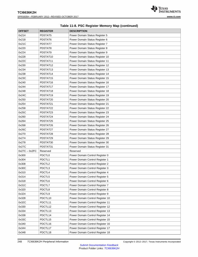
248
TCI6636K2HSPRS835H –FEBRUARY 2012–REVISED OCTOBER 2017 www.ti.com
Submit Documentation FeedbackProduct Folder Links: TCI6636K2H
TCI6636K2H Peripheral Information Copyright © 2012–2017, Texas Instruments Incorporated
Table 11-8. PSC Register Memory Map (continued)OFFSET REGISTER DESCRIPTION0x214 PDSTAT5 Power Domain Status Register 50x218 PDSTAT6 Power Domain Status Register 60x21C PDSTAT7 Power Domain Status Register 70x220 PDSTAT8 Power Domain Status Register 80x224 PDSTAT9 Power Domain Status Register 90x228 PDSTAT10 Power Domain Status Register 100x22C PDSTAT11 Power Domain Status Register 110x230 PDSTAT12 Power Domain Status Register 120x234 PDSTAT13 Power Domain Status Register 130x238 PDSTAT14 Power Domain Status Register 140x23C PDSTAT15 Power Domain Status Register 150x240 PDSTAT16 Power Domain Status Register 160x244 PDSTAT17 Power Domain Status Register 170x248 PDSTAT18 Power Domain Status Register 180x24C PDSTAT19 Power Domain Status Register 190x250 PDSTAT20 Power Domain Status Register 200x254 PDSTAT21 Power Domain Status Register 210x258 PDSTAT22 Power Domain Status Register 220x25C PDSTAT23 Power Domain Status Register 230x260 PDSTAT24 Power Domain Status Register 240x264 PDSTAT25 Power Domain Status Register 250x268 PDSTAT26 Power Domain Status Register 260x26C PDSTAT27 Power Domain Status Register 270x270 PDSTAT28 Power Domain Status Register 280x274 PDSTAT29 Power Domain Status Register 290x278 PDSTAT30 Power Domain Status Register 300x27C PDSTAT31 Power Domain Status Register 310x27C – 0x2FC Reserved Reserved0x300 PDCTL0 Power Domain Control Register 00x304 PDCTL1 Power Domain Control Register 10x308 PDCTL2 Power Domain Control Register 20x30C PDCTL3 Power Domain Control Register 30x310 PDCTL4 Power Domain Control Register 40x314 PDCTL5 Power Domain Control Register 50x318 PDCTL6 Power Domain Control Register 60x31C PDCTL7 Power Domain Control Register 70x320 PDCTL8 Power Domain Control Register 80x324 PDCTL9 Power Domain Control Register 90x328 PDCTL10 Power Domain Control Register 100x32C PDCTL11 Power Domain Control Register 110x330 PDCTL12 Power Domain Control Register 120x334 PDCTL13 Power Domain Control Register 130x338 PDCTL14 Power Domain Control Register 140x33C PDCTL15 Power Domain Control Register 150x340 PDCTL16 Power Domain Control Register 160x344 PDCTL17 Power Domain Control Register 170x348 PDCTL18 Power Domain Control Register 18

249
TCI6636K2Hwww.ti.com SPRS835H –FEBRUARY 2012–REVISED OCTOBER 2017
Submit Documentation FeedbackProduct Folder Links: TCI6636K2H
TCI6636K2H Peripheral InformationCopyright © 2012–2017, Texas Instruments Incorporated
Table 11-8. PSC Register Memory Map (continued)OFFSET REGISTER DESCRIPTION0x34C PDCTL19 Power Domain Control Register 190x350 PDCTL20 Power Domain Control Register 200x354 PDCTL21 Power Domain Control Register 210x358 PDCTL22 Power Domain Control Register 220x35c PDCTL23 Power Domain Control Register 230x360 PDCTL24 Power Domain Control Register 240x364 PDCTL25 Power Domain Control Register 250x368 PDCTL26 Power Domain Control Register 260x36C PDCTL27 Power Domain Control Register 270x370 PDCTL28 Power Domain Control Register 280x374 PDCTL29 Power Domain Control Register 290x378 PDCTL30 Power Domain Control Register 300x37C PDCTL31 Power Domain Control Register 310x380 – 0x7FC Reserved Reserved0x800 MDSTAT0 Module Status Register 0 (never gated)0x804 MDSTAT1 Module Status Register 10x808 MDSTAT2 Module Status Register 20x80C MDSTAT3 Module Status Register 30x810 MDSTAT4 Module Status Register 40x814 MDSTAT5 Module Status Register 50x818 MDSTAT6 Module Status Register 60x81C MDSTAT7 Module Status Register 70x820 MDSTAT8 Module Status Register 80x824 MDSTAT9 Module Status Register 90x828 MDSTAT10 Module Status Register 100x82C MDSTAT11 Module Status Register 110x830 MDSTAT12 Module Status Register 120x834 MDSTAT13 Module Status Register 130x838 MDSTAT14 Module Status Register 140x83C MDSTAT15 Module Status Register 150x840 MDSTAT16 Module Status Register 160x844 MDSTAT17 Module Status Register 170x848 MDSTAT18 Module Status Register 180x84C MDSTAT19 Module Status Register 190x850 MDSTAT20 Module Status Register 200x854 MDSTAT21 Module Status Register 210x858 MDSTAT22 Module Status Register 220x85C MDSTAT23 Module Status Register 230x860 MDSTAT24 Module Status Register 240x864 MDSTAT25 Module Status Register 250x868 MDSTAT26 Module Status Register 260x86C MDSTAT27 Module Status Register 270x870 MDSTAT28 Module Status Register 280x874 MDSTAT29 Module Status Register 290x878 MDSTAT30 Module Status Register 300x87C MDSTAT31 Module Status Register310x880 MDSTAT32 Module Status Register 32

250
TCI6636K2HSPRS835H –FEBRUARY 2012–REVISED OCTOBER 2017 www.ti.com
Submit Documentation FeedbackProduct Folder Links: TCI6636K2H
TCI6636K2H Peripheral Information Copyright © 2012–2017, Texas Instruments Incorporated
Table 11-8. PSC Register Memory Map (continued)OFFSET REGISTER DESCRIPTION0x884 MDSTAT33 Module Status Register 330x888 MDSTAT34 Module Status Register 340x88C MDSTAT35 Module Status Register 350x890 MDSTAT36 Module Status Register 360x894 MDSTAT37 Module Status Register 370x898 MDSTAT38 Module Status Register 380x89C MDSTAT39 Module Status Register 390x8A0 MDSTAT40 Module Status Register 400x8A4 MDSTAT41 Module Status Register 410x8A8 MDSTAT42 Module Status Register 420x8AC MDSTAT43 Module Status Register 430x8B0 MDSTAT44 Module Status Register 440x8B4 MDSTAT45 Module Status Register 450x8B8 MDSTAT46 Module Status Register 460x8BC MDSTAT47 Module Status Register 470x8C0 MDSTAT48 Module Status Register 480x8C4 MDSTAT49 Module Status Register 490x8C8 MDSTAT50 Module Status Register 500x8CC MDSTAT51 Module Status Register 510x8D0 MDSTAT52 Module Status Register 520x8D4 – 0x9FC Reserved Reserved0xA00 MDCTL0 Module Control Register 0 (never gated)0xA04 MDCTL1 Module Control Register 10xA08 MDCTL2 Module Control Register 20xA0C MDCTL3 Module Control Register 30xA10 MDCTL4 Module Control Register 40xA14 MDCTL5 Module Control Register 50xA18 MDCTL6 Module Control Register 60xA1C MDCTL7 Module Control Register 70xA20 MDCTL8 Module Control Register 80xA24 MDCTL9 Module Control Register 90xA28 MDCTL10 Module Control Register 100xA2C MDCTL11 Module Control Register 110xA30 MDCTL12 Module Control Register 120xA34 MDCTL13 Module Control Register 130xA38 MDCTL14 Module Control Register 140xA3C MDCTL15 Module Control Register 150xA40 MDCTL16 Module Control Register 160xA44 MDCTL17 Module Control Register 170xA48 MDCTL18 Module Control Register 180xA4C MDCTL19 Module Control Register 190xA50 MDCTL20 Module Control Register 200xA54 MDCTL21 Module Control Register 210xA58 MDCTL22 Module Control Register 220xA5C MDCTL23 Module Control Register 230xA60 MDCTL24 Module Control Register 240xA64 MDCTL25 Module Control Register 25

251
TCI6636K2Hwww.ti.com SPRS835H –FEBRUARY 2012–REVISED OCTOBER 2017
Submit Documentation FeedbackProduct Folder Links: TCI6636K2H
TCI6636K2H Peripheral InformationCopyright © 2012–2017, Texas Instruments Incorporated
Table 11-8. PSC Register Memory Map (continued)OFFSET REGISTER DESCRIPTION0xA68 MDCTL26 Module Control Register 260xA6C MDCTL27 Module Control Register 270xA70 MDCTL28 Module Control Register 280xA74 MDCTL29 Module Control Register 290xA78 MDCTL30 Module Control Register 300xA7C MDCTL31 Module Control Register310xA80 MDCTL32 Module Control Register 320xA84 MDCTL33 Module Control Register 330xA88 MDCTL34 Module Control Register 340xA8C MDCTL35 Module Control Register 350xA90 MDCTL36 Module Control Register 360xA94 MDCTL37 Module Control Register 370xA98 MDCTL38 Module Control Register 380xA9C MDCTL39 Module Control Register 390xAA0 MDCTL40 Module Control Register 400xAA4 MDCTL41 Module Control Register 410xAA8 MDCTL42 Module Control Register 420xAAC MDCTL43 Module Control Register 430xAB0 MDCTL44 Module Control Register 440xAB4 MDCTL45 Module Control Register 450xAB8 MDCTL46 Module Control Register 460xABC MDCTL47 Module Control Register 470xAC0 MDCTL48 Module Control Register 480xAC4 MDCTL49 Module Control Register 490xAC8 MDCTL50 Module Control Register 500xACC MDCTL51 Module Control Register 510xAD0 MDCTL52 Module Control Register 520xAD4 – 0xFFC Reserved Reserved
11.4 Reset ControllerThe reset controller detects the different type of resets supported on the TCI6636K2H device andmanages the distribution of those resets throughout the device. The device has the following types ofresets:• Power-on reset• Hard reset• Soft reset• Local reset
Table 11-9 explains further the types of reset, the reset initiator, and the effects of each reset on thedevice. For more information on the effects of each reset on the PLL controllers and their clocks, seeSection 11.4.8.
Table 11-9. Reset Types
TYPE INITIATOR EFFECT(S)Power-on reset POR pin Resets the entire chip including the test and emulation logic. The device configuration pins
are latched only during power-on reset.RESETFULL pin

252
TCI6636K2HSPRS835H –FEBRUARY 2012–REVISED OCTOBER 2017 www.ti.com
Submit Documentation FeedbackProduct Folder Links: TCI6636K2H
TCI6636K2H Peripheral Information Copyright © 2012–2017, Texas Instruments Incorporated
Table 11-9. Reset Types (continued)TYPE INITIATOR EFFECT(S)
(1) All masters in the device have access to the PLL control registers.
Hard reset RESET pin Hard reset resets everything except for test, emulation logic, and reset isolation modules.This reset is different from power-on reset in that the PLL Controller assumes power andclocks are stable when a hard reset is asserted. The device configurations pins are notrelatched.
Emulation-initiated reset is always a hard reset.
By default, these initiators are configured as hard reset, but can be configured (exceptemulation) as a soft reset in the RSCFG Register of the PLL Controller. Contents of theDDR3 SDRAM memory can be retained during a hard reset if the SDRAM is placed in self-refresh mode.
PLLCTL Register(RSCTRL) (1)
Watchdog timersEmulation
Soft reset RESET pin Soft reset behaves like hard reset except that PCIe MMRs (memory-mapped registers) andDDR3 EMIF MMRs contents are retained.
By default, these initiators are configured as hard reset, but can be configured as soft resetin the RSCFG Register of the PLL Controller. Contents of the DDR3 SDRAM memory canbe retained during a soft reset if the SDRAM is placed in self-refresh mode.
PLLCTL Register(RSCTRL)
Watchdog timers
Local reset LRESET pin Resets the C66x CorePac, without disturbing clock alignment or memory contents. Thedevice configuration pins are not relatched.Watchdog timer time-out
LPSC MMRs
11.4.1 Power-on ResetPower-on reset is used to reset the entire device, including the test and emulation logic.
Power-on reset is initiated by the following:1. POR pin2. RESETFULL pin
During power-up, the POR pin must be asserted (driven low) until the power supplies have reached theirnormal operating conditions. Also a RESETFULL pin is provided to allow reset of the entire device,including the reset-isolated logic, when the device is already powered up. For this reason, theRESETFULL pin, unlike POR, should be driven by the onboard host control other than the power goodcircuitry. For power-on reset, the Core PLL Controller comes up in bypass mode and the PLL is notenabled. Other resets do not affect the state of the PLL or the dividers in the PLL Controller.
The following sequence must be followed during a power-on reset:1. Wait for all power supplies to reach normal operating conditions while keeping the POR and
RESETFULL pins asserted (driven low). While POR is asserted, all pins except RESETSTAT will beset to high-impedance. After the POR pin is deasserted (driven high), all Z group pins, low group pins,and high group pins are set to their reset state and remain in their reset state until otherwiseconfigured by their respective peripheral. All peripherals that are power-managed are disabled after apower-on reset and must be enabled through the Device State Control Registers (for more details, seeSection 10.2.3).
2. Clocks are reset, and they are propagated throughout the chip to reset any logic that was using resetsynchronously. All logic is now reset and RESETSTAT is driven low, indicating that the device is inreset.
3. POR must be held active until all supplies on the board are stable, and then for at least an additionalperiod of time (as specified in Section 11.2.1) for the chip-level PLLs to lock.
4. The POR pin can now be deasserted. Reset-sampled pin values are latched at this point. Then, allchip-level PLLs are taken out of reset, locking sequences begin, and all power-on device initializationprocesses begin.
5. After device initialization is complete, the RESETSTAT pin is deasserted (driven high). By this time, theDDR3A PLL and DDR3B PLL have already completed their locking sequences and are supplying avalid clock. The system clocks of the PLL controllers are allowed to finish their current cycles and then

253
TCI6636K2Hwww.ti.com SPRS835H –FEBRUARY 2012–REVISED OCTOBER 2017
Submit Documentation FeedbackProduct Folder Links: TCI6636K2H
TCI6636K2H Peripheral InformationCopyright © 2012–2017, Texas Instruments Incorporated
are paused for 10 cycles of their respective system reference clocks. After the pause, the systemclocks are restarted at their default divide-by settings.
6. The device is now out of reset and code execution begins as dictated by the selected boot mode.
NOTETo most of the device, reset is deasserted only when the POR and RESET pins are bothdeasserted (driven high). Therefore, in the sequence described above, if the RESET pin isheld low past the low period of the POR pin, most of the device will remain in reset. TheRESET pin should not be tied to the POR pin.
11.4.2 Hard ResetA hard reset will reset everything on the device except the PLLs, test logic, emulation logic, and reset-isolated modules. POR should also remain deasserted during this time.
Hard reset is initiated by the following:• RESET pin• RSCTRL Register in the PLL Controller• Watchdog timer• Emulation
By default, all the initiators listed above are configured to generate a hard reset. Except for emulation, allof the other three initiators can be configured in the RSCFG Register in the PLL Controller to generate softresets.
The following sequence must be followed during a hard reset:1. The RESET pin is asserted (driven low) for a minimum of 24 CLKIN1 cycles. During this time, the
RESET signal propagates to all modules (except those specifically mentioned above). To prevent off-chip contention during the warm reset, all I/O must be Hi-Z for modules affected by RESET.
2. Once all logic is reset, RESETSTAT is asserted (driven low) to denote that the device is in reset.3. The RESET pin can now be released. A minimal device initialization begins to occur. Note that
configuration pins are not relatched and clocking is unaffected within the device.4. After device initialization is complete, the RESETSTAT pin is deasserted (driven high).
NOTEThe POR pin should be held inactive (high) throughout the warm reset sequence. Otherwise,if POR is activated (brought low), the minimum POR pulse width must be met. The RESETpin should not be tied to the POR pin.
11.4.3 Soft ResetA soft reset behaves like a hard reset except that the EMIF16 MMRs, DDR3A EMIF MMRs, PCIe MMRssticky bits, and external memory content are retained. POR should also remain deasserted during thistime.
Soft reset is initiated by the following:• RESET pin• RSCTRL Register in the PLL Controller• Watchdog timer
254
TCI6636K2HSPRS835H –FEBRUARY 2012–REVISED OCTOBER 2017 www.ti.com
Submit Documentation FeedbackProduct Folder Links: TCI6636K2H
TCI6636K2H Peripheral Information Copyright © 2012–2017, Texas Instruments Incorporated
In the case of a soft reset, the clock logic and the power control logic of the peripherals are not affectedand, therefore, the enabled/disabled state of the peripherals is not affected. On a soft reset, the DDR3Aand DDR3B memory controller registers are not reset. If the user places the DDR3A and DDR3B SDRAMin self-refresh mode before invoking the soft reset, the DDR3A and DDR3B SDRAM memory content isretained.
During a soft reset, the following occurs:1. The RESETSTAT pin goes low to indicate an internal reset is being generated. The reset propagates
through the system. Internal system clocks are not affected. PLLs remain locked.2. After device initialization is complete, the RESETSTAT pin is deasserted (driven high). In addition, the
PLL Controller pauses system clocks for approximately eight cycles. At this point:– The peripherals remain in the state they were in before the soft reset.– The states of the Boot Mode configuration pins are preserved as controlled by the DEVSTAT
Register.– The DDR3A and DDR3B MMRs and PCIe MMRs retain their previous values. Only the DDR3A and
DDR3B memory controller and PCIe state machines are reset by the soft reset.– The PLL Controller remains in the mode it was in before the soft reset.– System clocks are unaffected.
The boot sequence is started after the system clocks are restarted. Because the Boot Mode configurationpins are not latched with a soft reset, the previous values (as shown in the DEVSTAT Register), are usedto select the boot mode.
11.4.4 Local ResetThe local reset can be used to reset a particular C66x CorePac without resetting any other devicecomponents.
Local reset is initiated by the following:• LRESET pin• Watchdog timer should cause one of the below based on the setting of the CORESEL[2:0] and
RSTCFG registers in the PLL Controller. (See Section 11.5.2.8 and Section 8.3.2.)– Local reset– NMI– NMI followed by a time delay and then a local reset for the C66x CorePac selected– Hard reset by requesting reset via the PLL Controller
• LPSC MMRs (memory-mapped registers)
For more details see the KeyStone Architecture Phase Locked Loop (PLL) Controller User's Guide.
11.4.5 ARM CorePac ResetThe ARM CorePac uses a combination of power-on-reset and module-reset to reset its components, suchas the Cortex-A15 processor, memory subsystem, debug logic, and so forth. The ARM CorePacincorporates the PSC to generate resets for its internal modules. Details of reset generation anddistribution inside the ARM CorePac can be found in the KeyStone II Architecture ARM CorePac User'sGuide.
11.4.6 Reset PriorityIf any of the previously mentioned reset sources occur simultaneously, the PLL Controller processes onlythe highest priority reset request. The reset request priorities are as follows (high to low):• Power-on reset• Hard/soft reset

255
TCI6636K2Hwww.ti.com SPRS835H –FEBRUARY 2012–REVISED OCTOBER 2017
Submit Documentation FeedbackProduct Folder Links: TCI6636K2H
TCI6636K2H Peripheral InformationCopyright © 2012–2017, Texas Instruments Incorporated
11.4.7 Reset Controller RegisterThe reset controller registers are part of the PLL Controller MMRs. All TCI6636K2H device-specific MMRsare covered in Section 11.5.2. For more details on these registers and how to program them, see theKeyStone Architecture Phase Locked Loop (PLL) Controller User's Guide.
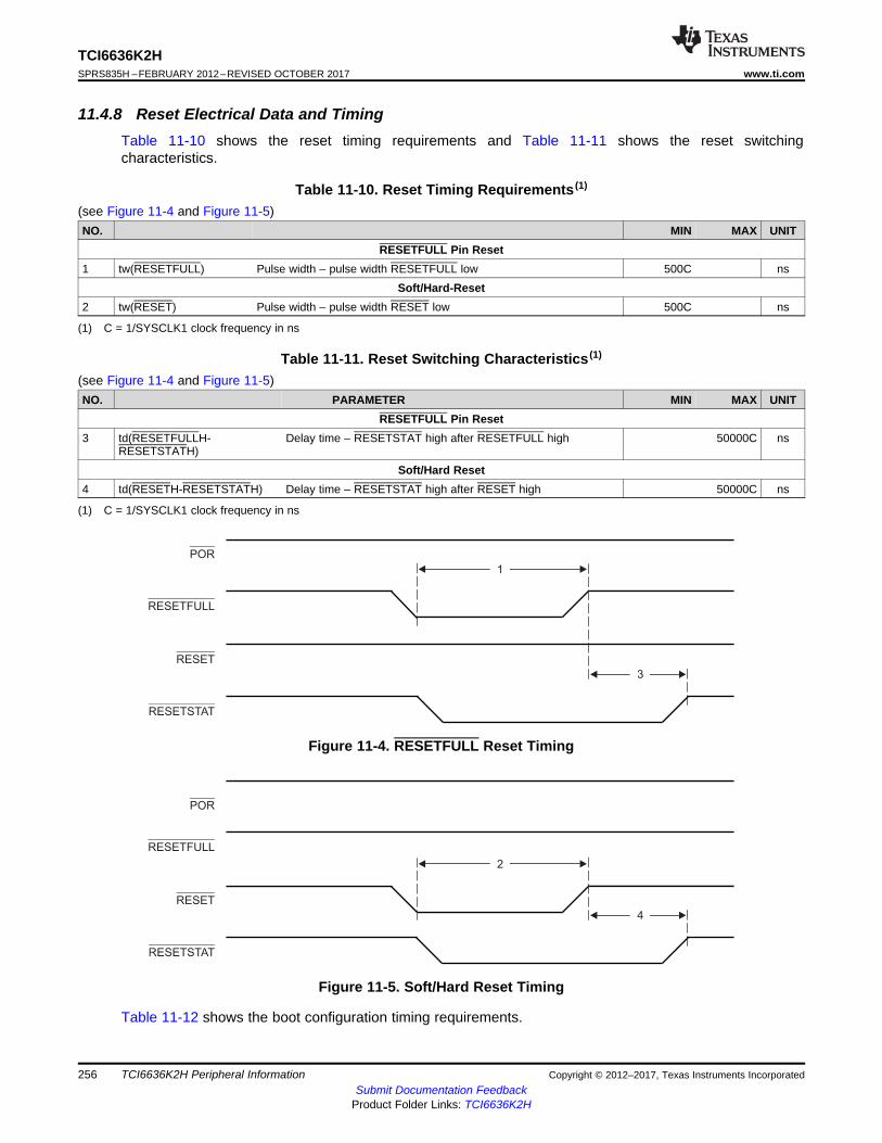
4
POR
RESET
RESETFULL
RESETSTAT
2
3
POR
RESET
RESETFULL
RESETSTAT
1
256
TCI6636K2HSPRS835H –FEBRUARY 2012–REVISED OCTOBER 2017 www.ti.com
Submit Documentation FeedbackProduct Folder Links: TCI6636K2H
TCI6636K2H Peripheral Information Copyright © 2012–2017, Texas Instruments Incorporated
11.4.8 Reset Electrical Data and TimingTable 11-10 shows the reset timing requirements and Table 11-11 shows the reset switchingcharacteristics.
(1) C = 1/SYSCLK1 clock frequency in ns
Table 11-10. Reset Timing Requirements (1)
(see Figure 11-4 and Figure 11-5)NO. MIN MAX UNIT
RESETFULL Pin Reset1 tw(RESETFULL) Pulse width – pulse width RESETFULL low 500C ns
Soft/Hard-Reset2 tw(RESET) Pulse width – pulse width RESET low 500C ns
(1) C = 1/SYSCLK1 clock frequency in ns
Table 11-11. Reset Switching Characteristics (1)
(see Figure 11-4 and Figure 11-5)NO. PARAMETER MIN MAX UNIT
RESETFULL Pin Reset3 td(RESETFULLH-
RESETSTATH)Delay time – RESETSTAT high after RESETFULL high 50000C ns
Soft/Hard Reset4 td(RESETH-RESETSTATH) Delay time – RESETSTAT high after RESET high 50000C ns
Figure 11-4. RESETFULL Reset Timing
Figure 11-5. Soft/Hard Reset Timing
Table 11-12 shows the boot configuration timing requirements.

1
RESETFULL
GPIO[15:0]
2
POR
257
TCI6636K2Hwww.ti.com SPRS835H –FEBRUARY 2012–REVISED OCTOBER 2017
Submit Documentation FeedbackProduct Folder Links: TCI6636K2H
TCI6636K2H Peripheral InformationCopyright © 2012–2017, Texas Instruments Incorporated
(1) C = 1/SYSCLK1 clock frequency in ns.
Table 11-12. Boot Configuration Timing Requirements (1)
(see Figure 11-6)NO. MIN MAX UNIT1 tsu(GPIOn-RESETFULL) Setup time – GPIO valid before RESETFULL asserted 12C ns2 th(RESETFULL-GPIOn) Hold time – GPIO valid after RESETFULL asserted 12C ns
Figure 11-6. Boot Configuration Timing
11.5 Main PLL, ARM PLL, DDR3A PLL, DDR3B PLL, PASS PLL and the PLL ControllersThis section provides a description of the Main PLL, ARM PLL, DDR3A PLL, DDR3B PLL, PASS PLL, andthe PLL Controller. For details on the operation of the PLL Controller module, see the KeyStoneArchitecture Phase Locked Loop (PLL) Controller User's Guide.
The Main PLL is controlled by the standard PLL Controller. The PLL Controller manages the clock ratios,alignment, and gating for the system clocks to the device. By default, the device powers up with the mainPLL bypassed. Figure 11-7 shows a block diagram of the Main PLL and the PLL Controller.
The ARM PLL, DDR3A PLL, DDR3B PLL, and PASS PLL are used to provide dedicated clock to the ARMCorePac, DDR3A, DDR3B, and PASS respectively. These chip level PLLs support a wide range ofmultiplier and divider values, which can be programmed through the chip level registers in the DeviceControl register block. The Boot ROM will program the multiplier values for main PLL, ARM PLL andPASS PLL based on boot mode. (See Section 10 for more details.)
The DDR3A PLL and DDR3B PLL are used to supply clocks to DDR3A and DDR3B EMIF logic. ThesePLLs can also be used without programming the PLL Controller. Instead, they can be controlled using thechip-level registers (DDR3APLLCTL0, DDR3APLLCTL1, DDR3BPLLCTL0, DDR3BPLLCTL1) in theDevice Control register block. To write to these registers, software must go through an unlockingsequence using the KICK0/KICK1 registers.
The multiplier values for all chip-level PLLs can be reprogrammed later based on the input parametertable. This feature provides flexibility in that these PLLs may be able to reuse other clock sources insteadof having its own clock source.

SYSCLK4
/zPLLDIV4
SYSCLK3
/xPLLDIV3
SYSCLK2
/1PLLDIV2
To Switch Fabric,Accelerators, SRIO,SmartReflex, and so forth
PLL ControllerC66x
CorePacs
SYSCLK1
/1PLLDIV1
POSTDIV
To Peripherals,HyperLink, and so forth
SYSCLK1
PLLOUT
SYSCLK(N|P)
ALTCORECLK(N|P)
CORECLKSELPLLD
VCO
PLLM PLL
CLKOD
BYPASS
0
1
Copyright © 2016, Texas Instruments Incorporated
258
TCI6636K2HSPRS835H –FEBRUARY 2012–REVISED OCTOBER 2017 www.ti.com
Submit Documentation FeedbackProduct Folder Links: TCI6636K2H
TCI6636K2H Peripheral Information Copyright © 2012–2017, Texas Instruments Incorporated
Figure 11-7. Main PLL and PLL Controller
The Main PLL Controller registers can be accessed by any master in the device. The PLLM[5:0] bits of themultiplier are controlled by the PLLM Register inside the PLL Controller and the PLLM[12:6] bits arecontrolled by the chip-level MAINPLLCTL0 Register. The output divide and bypass logic of the PLL arecontrolled by fields in the SECCTL Register in the PLL Controller. Only PLLDIV3, and PLLDIV4 areprogrammable on the device. See the KeyStone Architecture Phase Locked Loop (PLL) Controller User'sGuide for more details on how to program the PLL controller.
The multiplication and division ratios within the PLL and the post-division for each of the chip-level clocksare determined by a combination of this PLL and the Main PLL Controller. The Main PLL Controller alsocontrols reset propagation through the chip, clock alignment, and test points. The Main PLL Controllermonitors the PLL status and provides an output signal indicating when the PLL is locked.
Main PLL power is supplied externally via the Main PLL power-supply pin (AVDDA1). An external EMIfilter circuit must be added to all PLL supplies. See Hardware Design Guide for KeyStone II Devices fordetailed recommendations. For the best performance, TI recommends that all the PLL externalcomponents be on a single side of the board without jumpers, switches, or components other than thoseshown. For reduced PLL jitter, maximize the spacing between switching signal traces and the PLLexternal components (C1, C2, and the EMI Filter).
The minimum SYSCLK rise and fall times should also be observed. For the input clock timingrequirements, see Section 11.5.5.
It should be assumed that any registers not included in these sections are not supported by the device.Furthermore, only the bits within the registers described here are supported. Avoid writing to any reservedmemory location or changing the value of reserved bits.
The PLL Controller module as described in the KeyStone Architecture Phase Locked Loop (PLL)Controller User's Guide includes a superset of features, some of which are not supported on theTCI6636K2H device. The following sections describe the registers that are supported.

259
TCI6636K2Hwww.ti.com SPRS835H –FEBRUARY 2012–REVISED OCTOBER 2017
Submit Documentation FeedbackProduct Folder Links: TCI6636K2H
TCI6636K2H Peripheral InformationCopyright © 2012–2017, Texas Instruments Incorporated
11.5.1 Main PLL Controller Device-Specific Information
11.5.1.1 Internal Clocks and Maximum Operating Frequencies
The Main PLL, used to drive the C66x CorePacs, the switch fabric, and a majority of the peripheral clocks(all but theARM CorePacs, DDR3, and the PASS modules) requires a PLL Controller to manage thevarious clock divisions, gating, and synchronization. Unlike other PLL, CLKOD functionality of Main PLL isreplaced by PLL controller Post-Divider register (POSTDIV). The POSTDIV.RATIO[3:0] andPOSTDIV.POSTDEN bits control the post divider ratio and divider enable respectively. PLLM[5:0] input ofthe Main PLL is controlled by the PLL controller PLLM register.
The Main PLL Controller has four SYSCLK outputs that are listed below, along with the clock descriptions.Each SYSCLK has a corresponding divider that divides down the output clock of the PLL. Note thatdividers are not programmable unless explicitly mentioned in the description below.• SYSCLK1: Full-rate clock for all C66x CorePacs. Using local dividers, SYSCLK1 is used to derive
clocks required for the majority of peripherals that do not need reset isolation.The system peripherals and modules driven by SYSCLK1 are as follows; however, not all peripheralsare supported in every part. See the Features chapter for the complete list of peripherals supported inyour part.AIF2, BCP, FFTC, RAC, TAC, TCP3d, VCP2, EMIF16, USB 3.0, USIM, HyperLink, PCIe, SGMII,SRIO, GPIO, Timer64, I2C, SPI, TeraNet, UART, ROM, CIC, Security Manager, BootCFG, PSC,Queue Manager, Semaphore, MPUs, EDMA, MSMC, DDR3, EMIF.
• SYSCLK2: Full-rate, reset-isolated clock used to generate various other clocks required by peripheralsthat need reset isolation: for example, SmartReflex and SRIO.
• SYSCLK3: 1/x-rate clock used to clock the C66x CorePac emulation. The default rate for this clock is1/3. This clock is programmable from /1 to /32, where this clock does not violate the maximum of 350MHz. SYSCLK3 can be turned off by software.
• SYSCLK4: 1/z-rate clock for the system trace module only. The default rate for this clock is 1/5. Thisclock is configurable: the maximum configurable clock is 210 MHz and the minimum configurationclock is 32 MHz. SYSCLK4 can be turned off by software.
• SYSCLK5: Slow, free running clock. The default rate for this clock is 1/24. SYSCLK5 cannot be turnedoff by software.
Only SYSCLK3, SYSCLK4, and SYSCLK5 are programmable.
11.5.1.2 Local Clock Dividers
The clock signals from the Main PLL Controller are routed to various modules and peripherals on thedevice. Some modules and peripherals have one or more internal clock dividers. Other modules andperipherals have no internal clock dividers, but are grouped together and receive clock signals from ashared local clock divider. Internal and shared local clock dividers have fixed division ratios, as shown inTable 11-13.

260
TCI6636K2HSPRS835H –FEBRUARY 2012–REVISED OCTOBER 2017 www.ti.com
Submit Documentation FeedbackProduct Folder Links: TCI6636K2H
TCI6636K2H Peripheral Information Copyright © 2012–2017, Texas Instruments Incorporated
Table 11-13. Main PLL Controller Module Clock Domains Internal and Shared Local Clock Dividers
CLOCK MODULEINTERNAL CLOCKDIVIDER(S)
SHARED LOCAL CLOCKDIVIDER
SYSCLK1 Internal Clock Dividers
SYSCLK1
Antenna Interface Subsystem 2 (AIF2) /3, /4, /6 --ARM CorePac /1, /3, /3, /6, /6 --Bit Rate Coprocessor (BCP) /3 --C66x DSP CorePacs /1, /2, /3, /4 --Chip Interrupt Controllers (CICx) /6 --DDR3 Memory Controller A (also receives clocks from theDDR3A_PLL)
/2 --
DDR3 Memory Controller B (also receives clocks from theDDR3B_PLL)
/3 --
EMIF16 /6 --Enhanced Viterbi-Decoder Coprocessor (VCP) /3 --Fast Fourier Transform Coprocessor (FFTC) /3 --HyperLink /2, /3, /6 --Multicore Navigator Queue Manager /3 --MultiCore Shared Memory Controller (MSMC) /1 --PCI express (PCIe) /2, /3, /4, /6 --Receive Accelerator Coprocessor (RAC) /3, /4 --ROM /6 --Serial Gigabit Media Independent Interface (SGMII) /2, /3, /6, /8 --Transmit Accelerator Coprocessor (TAC) /3 --Turbo Decoder Coprocessor (TCP3d) /2, /3 --Universal Asynchronous Receiver/Transmitter (UART) /6 --Universal Serial Bus 3.0 (USB 3.0) /3, /6 --
SYSCLK1 Shared Local Clock Dividers
SYSCLK1
Power/Sleep Controller (PSC) -- /12, /24EDMA
-- /3Memory Protection Units (MPUx)SemaphoreTeraNet (SYSCLK1/3 domain)
SYSCLK1
Boot Config
-- /6
General-Purpose Input/Output (GPIO)I2CSecurity ManagerSerial Peripheral Interconnect (SPI)TeraNet (CPU /6 domain)TimersUniversal Subscriber Identity Module (USIM)
SYSCLK2 Internal Clock Dividers
SYSCLK2Serial RapidIO (SRIO) /3, /4, /6 --SmartReflex C66x CorePacs /12, /128 --SmartReflex ARM CorePac /12, /128, /128 --
11.5.1.3 Module Clock Input
Table 11-7 lists various clock domains in the device and their distribution in each peripheral. The tablealso shows the distributed clock division in modules and their mapping with source clocks of the devicePLLs.

261
TCI6636K2Hwww.ti.com SPRS835H –FEBRUARY 2012–REVISED OCTOBER 2017
Submit Documentation FeedbackProduct Folder Links: TCI6636K2H
TCI6636K2H Peripheral InformationCopyright © 2012–2017, Texas Instruments Incorporated
(1) C = SYSCLK1(N|P) cycle time in ns.
11.5.1.4 Main PLL Controller Operating Modes
The Main PLL Controller has two modes of operation: bypass mode and PLL mode. The mode ofoperation is determined by the BYPASS bit of the PLL Secondary Control Register (SECCTL).• In bypass mode, PLL input is fed directly out as SYSCLK1.• In PLL mode, SYSCLK1 is generated from the PLL output using the values set in the PLLM and PLLD
fields in the MAINPLLCTL0 Register.
External hosts must avoid access attempts to the DSP while the frequency of its internal clocks ischanging. User software must implement a mechanism that causes the DSP to notify the host when thePLL configuration has completed.
11.5.1.5 Main PLL Stabilization, Lock, and Reset Times
The PLL stabilization time is the amount of time that must be allotted for the internal PLL regulators tobecome stable after device power-up. The device should not be taken out of reset until this stabilizationtime has elapsed.
The PLL reset time is the amount of wait time needed when resetting the PLL (writing PLLRST = 1), inorder for the PLL to properly reset, before bringing the PLL out of reset (writing PLLRST = 0). For theMain PLL reset time value, see Table 11-14.
The PLL lock time is the amount of time needed from when the PLL is taken out of reset to when the PLLController can be switched to PLL mode. The Main PLL lock time is given in Table 11-14 .
Table 11-14. Main PLL Stabilization, Lock, and Reset Times
PARAMETER MIN TYP MAX UNITPLL stabilization time 100 µsPLL lock time 2000 × C (1)
PLL reset time 1000 ns
11.5.2 PLL Controller Memory MapThe memory map of the Main PLL controller is shown in Table 11-15. TCI6636K2H-specific Main PLLcontroller register definitions can be found in the sections following Table 11-15. For other registers in thetable, see the KeyStone Architecture Phase Locked Loop (PLL) Controller User's Guide.
It is recommended to use read-modify-write sequence to make any changes to the valid bits in the MainPLL controller registers.
Note that only registers documented here are accessible on the TCI6636K2H. Other addresses in theMain PLL controller memory map including the Reserved registers must not be modified. Furthermore,only the bits within the registers described here are supported.
Table 11-15. PLL Controller Registers (Including Reset Controller)
HEX ADDRESS RANGE ACRONYM REGISTER NAME00 0231 0000 – 00 0231 00E3 - Reserved00 0231 00E4 RSTYPE Reset Type Status Register (Reset Main PLL Controller)00 0231 00E8 RSTCTRL Software Reset Control Register (Reset Main PLL Controller)00 0231 00EC RSTCFG Reset Configuration Register (Reset Main PLL Controller)00 0231 00F0 RSISO Reset Isolation Register (Reset Main PLL Controller)00 0231 00F0 – 00 0231 00FF - Reserved00 0231 0100 PLLCTL PLL Control Register00 0231 0104 - Reserved00 0231 0108 SECCTL PLL Secondary Control Register

262
TCI6636K2HSPRS835H –FEBRUARY 2012–REVISED OCTOBER 2017 www.ti.com
Submit Documentation FeedbackProduct Folder Links: TCI6636K2H
TCI6636K2H Peripheral Information Copyright © 2012–2017, Texas Instruments Incorporated
Table 11-15. PLL Controller Registers (Including Reset Controller) (continued)HEX ADDRESS RANGE ACRONYM REGISTER NAME00 0231 010C - Reserved00 0231 0110 PLLM PLL Multiplier Control Register00 0231 0114 - Reserved00 0231 0118 PLLDIV1 PLL Controller Divider 1 Register00 0231 011C PLLDIV2 PLL Controller Divider 2 Register00 0231 0120 PLLDIV3 PLL Controller Divider 3 Register00 0231 0124 - Reserved00 0231 0128 POSTDIV PLL Controller Post-Divide Register00 0231 012C – 00 0231 0134 - Reserved00 0231 0138 PLLCMD PLL Controller Command Register00 0231 013C PLLSTAT PLL Controller Status Register00 0231 0140 ALNCTL PLL Controller Clock Align Control Register00 0231 0144 DCHANGE PLLDIV Ratio Change Status Register00 0231 0148 CKEN Reserved00 0231 014C CKSTAT Reserved00 0231 0150 SYSTAT SYSCLK Status Register00 0231 0154 – 00 0231 015C - Reserved00 0231 0160 PLLDIV4 PLL Controller Divider 4 Register00 0231 0164 PLLDIV5 Reserved00 0231 0168 PLLDIV6 Reserved00 0231 016C PLLDIV7 Reserved00 0231 0170 PLLDIV8 Reserved00 0231 0174 – 00 0231 0193 PLLDIV9 – PLLDIV16 Reserved00 0231 0194 – 00 0231 01FF - Reserved
11.5.2.1 PLL Secondary Control Register (SECCTL)
The PLL secondary control register contains extra fields to control the Main PLL and is shown inFigure 11-8 and described in Table 11-16.
Figure 11-8. PLL Secondary Control Register (SECCTL)31 30 29 28 27 26 25 24 23 22 21 20 19 18 17 16 15 14 13 12 11 10 9 8 7 6 5 4 3 2 1 0
Reserved BYPASS OUTPUT DIVIDE Reserved
R-0000 0000 RW-1 RW-0001 RW-001 0000 0000 0000 0000
Legend: R/W = Read/Write; R = Read only; – n = value after reset
Table 11-16. PLL Secondary Control Register Field DescriptionsBit Field Description31-24 Reserved Reserved23 BYPASS PLL bypass mode:
• 0 = PLL is not in BYPASS mode• 1 = PLL is in BYPASS mode
22-19 OUTPUT DIVIDE Output divider ratio bits• 0h = ÷1. Divide frequency by 1• 1h = ÷2. Divide frequency by 2• 2h = ÷3. Divide frequency by 3• 3h = ÷4. Divide frequency by 4• 4h – Fh = ÷5 to ÷16. Divide frequency range: divide frequency by 5 to divide frequency by 80.
18-0 Reserved Reserved

263
TCI6636K2Hwww.ti.com SPRS835H –FEBRUARY 2012–REVISED OCTOBER 2017
Submit Documentation FeedbackProduct Folder Links: TCI6636K2H
TCI6636K2H Peripheral InformationCopyright © 2012–2017, Texas Instruments Incorporated
11.5.2.2 PLL Controller Divider Register (PLLDIV3 and PLLDIV4)
The PLL controller divider registers (PLLDIV3 and PLLDIV4) are shown in Figure 11-9 and described inTable 11-17. The default values of the RATIO field on a reset for PLLDIV3, and PLLDIV4 are different asmentioned in the footnote of Figure 11-9 .
(1) D3EN for PLLDIV3; D4EN for PLLDIV4(2) n=02h for PLLDIV3; n=03h for PLLDIV4
Figure 11-9. PLL Controller Divider Register (PLLDIVn)31 30 29 28 27 26 25 24 23 22 21 20 19 18 17 16 15 14 13 12 11 10 9 8 7 6 5 4 3 2 1 0
Reserved Dn (1)EN Reserved RATIO
R-0 R/W-1 R-0 R/W-n (2)
Legend: R/W = Read/Write; R = Read only; – n = value after reset
Table 11-17. PLL Controller Divider Register Field DescriptionsBit Field Description31-16 Reserved Reserved15 DnEN Divider Dn enable bit (See footnote of Figure 11-9 )
• 0 = Divider n is disabled• 1 = No clock output. Divider n is enabled.
14-8 Reserved Reserved. The reserved bit location is always read as 0. A value written to this field has no effect.7-0 RATIO Divider ratio bits (See footnote of Figure 11-9 )
• 0h = ÷1. Divide frequency by 1• 1h = ÷2. Divide frequency by 2• 2h = ÷3. Divide frequency by 3• 3h = ÷4. Divide frequency by 4• 4h – 4Fh = ÷5 to ÷80. Divide frequency range: divide frequency by 5 to divide frequency by 80.
11.5.2.3 PLL Controller Clock Align Control Register (ALNCTL)
The PLL controller clock align control register (ALNCTL) is shown in Figure 11-10 and described inTable 11-18.
Figure 11-10. PLL Controller Clock Align Control Register (ALNCTL)31 30 29 28 27 26 25 24 23 22 21 20 19 18 17 16 15 14 13 12 11 10 9 8 7 6 5 4 3 2 1 0
Reserved ALN4 ALN3 Reserved
R-0 R/W-1 R/W-1 R-0
Legend: R/W = Read/Write; R = Read only; – n = value after reset, for reset value
Table 11-18. PLL Controller Clock Align Control Register Field DescriptionsBit Field Description31-5 Reserved Reserved. This location is always read as 0. A value written to this field has no effect.4-3 ALN[4:3] SYSCLKn alignment. Do not change the default values of these fields.
• 0 = Do not align SYSCLKn to other SYSCLKs during GO operation. If SYSn in DCHANGE is set, SYSCLKnswitches to the new ratio immediately after the GOSET bit in PLLCMD is set.
• 1 = Align SYSCLKn to other SYSCLKs selected in ALNCTL when the GOSET bit in PLLCMD is set and SYSnin DCHANGE is 1. The SYSCLKn rate is set to the ratio programmed in the RATIO bit in PLLDIVn.
2-0 Reserved Reserved. This location is always read as 0. A value written to this field has no effect.
11.5.2.4 PLLDIV Divider Ratio Change Status Register (DCHANGE)
Whenever a different ratio is written to the PLLDIVn registers, the PLL CTL flags the change in theDCHANGE status register. During the GO operation, the PLL controller changes only the divide ratio ofthe SYSCLKs with the bit set in DCHANGE. Note that the ALNCTL register determines if that clock alsoneeds to be aligned to other clocks. The PLLDIV divider ratio change status register is shown inFigure 11-11 and described in Table 11-19.
264
TCI6636K2HSPRS835H –FEBRUARY 2012–REVISED OCTOBER 2017 www.ti.com
Submit Documentation FeedbackProduct Folder Links: TCI6636K2H
TCI6636K2H Peripheral Information Copyright © 2012–2017, Texas Instruments Incorporated
Figure 11-11. PLLDIV Divider Ratio Change Status Register (DCHANGE)31 30 29 28 27 26 25 24 23 22 21 20 19 18 17 16 15 14 13 12 11 10 9 8 7 6 5 4 3 2 1 0
Reserved SYS4 SYS3 Reserved
R-0 R/W-1 R/W-1 R-0
Legend: R/W = Read/Write; R = Read only; – n = value after reset, for reset value
Table 11-19. PLLDIV Divider Ratio Change Status Register Field DescriptionsBit Field Description31-5 Reserved Reserved. This bit location is always read as 0. A value written to this field has no effect.4-3 SYS[4:3] Identifies when the SYSCLKn divide ratio has been modified.
• 0 = SYSCLKn ratio has not been modified. When GOSET is set, SYSCLKn will not be affected.• 1 = SYSCLKn ratio has been modified. When GOSET is set, SYSCLKn will change to the new ratio.
2-0 Reserved Reserved. This bit location is always read as 0. A value written to this field has no effect.
11.5.2.5 SYSCLK Status Register (SYSTAT)
The SYSCLK status register (SYSTAT) shows the status of SYSCLK[4:1]. SYSTAT is shown in Figure 11-12 and described in Table 11-20.
Figure 11-12. SYSCLK Status Register (SYSTAT)31 30 29 28 27 26 25 24 23 22 21 20 19 18 17 16 15 14 13 12 11 10 9 8 7 6 5 4 3 2 1 0
Reserved SYS4ON
SYS3ON
SYS2ON
SYS1ON
R-n R-1 R-1 R-1 R-1
Legend: R/W = Read/Write; R = Read only; – n = value after reset
(1) Where N = 1, 2, 3, or 4
Table 11-20. SYSCLK Status Register Field DescriptionsBit Field Description31-4 Reserved Reserved. This location is always read as 0. A value written to this field has no effect.3-0 SYS[N]ON (1) SYSCLK[N] on status
• 0 = SYSCLK[N] is gated• 1 = SYSCLK[N] is on
11.5.2.6 Reset Type Status Register (RSTYPE)
The reset type status register (RSTYPE) latches the cause of the last reset. If multiple reset sources occursimultaneously, this register latches the highest priority reset source. The reset type status register isshown in Figure 11-13 and described in Table 11-21.
Figure 11-13. Reset Type Status Register (RSTYPE)31 30 29 28 27 26 25 24 23 22 21 20 19 18 17 16 15 14 13 12 11 10 9 8 7 6 5 4 3 2 1 0
Reserved EMU-RST Reserved WDRST[N] Reserved PLLCTRL
RST RESET POR
R-0 R-0 R-0 R-0 R-0 R-0 R-0 R-0
Legend: R = Read only; – n = value after reset
Table 11-21. Reset Type Status Register Field DescriptionsBit Field Description31-29 Reserved Reserved. Always reads as 0. Writes have no effect.28 EMU-RST Reset initiated by emulation
• 0 = Not the last reset to occur• 1 = The last reset to occur
27-12 Reserved Reserved. Always reads as 0. Writes have no effect.

265
TCI6636K2Hwww.ti.com SPRS835H –FEBRUARY 2012–REVISED OCTOBER 2017
Submit Documentation FeedbackProduct Folder Links: TCI6636K2H
TCI6636K2H Peripheral InformationCopyright © 2012–2017, Texas Instruments Incorporated
Table 11-21. Reset Type Status Register Field Descriptions (continued)Bit Field Description11-8 WDRST[3:0] Reset initiated by Watchdog Timer[N]
• 0 = Not the last reset to occur• 1 = The last reset to occur
7-3 Reserved Reserved. Always reads as 0. Writes have no effect.2 PLLCTLRST Reset initiated by PLLCTL
• 0 = Not the last reset to occur• 1 = The last reset to occur
1 RESET RESET reset• 0 = RESET was not the last reset to occur• 1 = RESET was the last reset to occur
0 POR Power-on reset• 0 = Power-on reset was not the last reset to occur• 1 = Power-on reset was the last reset to occur
11.5.2.7 Reset Control Register (RSTCTRL)
This register contains a key that enables writes to the MSB of this register and the RSTCFG register. Thekey value is 0x5A69. A valid key will be stored as 0x000C. Any other key value is invalid. When theRSTCTRL or the RSTCFG is written, the key is invalidated. Every write must be set up with a valid key.The software reset control register (RSTCTRL) is shown in Figure 11-14 and described in Table 11-22.
(1) Writes are conditional based on valid key.
Figure 11-14. Reset Control Register (RSTCTRL)31 30 29 28 27 26 25 24 23 22 21 20 19 18 17 16 15 14 13 12 11 10 9 8 7 6 5 4 3 2 1 0
Reserved SWRST KEY
R-0x0000 R/W-0x (1)
R/W-0x0003
Legend: R = Read only; – n = value after reset;
Table 11-22. Reset Control Register Field DescriptionsBit Field Description31-17 Reserved Reserved16 SWRST Software reset
• 0 = Reset• 1 = Not reset
15-0 KEY Key used to enable writes to RSTCTRL and RSTCFG.
11.5.2.8 Reset Configuration Register (RSTCFG)
This register is used to configure the type of reset (a hard reset or a soft reset) initiated by RESET, thewatchdog timer, and the RSTCTRL register of the Main PLL controller. By default, these resets are hardresets. The RSTCFG is shown in Figure 11-15 and described in Table 11-23.
(1) Where N = 1, 2, 3,....N (Not all these outputs may be used on a specific device.)(2) Writes are conditional based on valid key. For details, see Section 11.5.2.7.
Figure 11-15. Reset Configuration Register (RSTCFG)31 30 29 28 27 26 25 24 23 22 21 20 19 18 17 16
Reserved
R-0x000000
15 14 13 12 11 10 9 8 7 6 5 4 3 2 1 0
Reserved PLLCTLRSTTYPE
RESETTYPE Reserved WDTYPE[N](1)
R-0x000000 R/W-0 (2) R/W-0(2) R-0x0 R/W-0x00(2)
Legend: R = Read only; R/W = Read/Write; – n = value after reset

266
TCI6636K2HSPRS835H –FEBRUARY 2012–REVISED OCTOBER 2017 www.ti.com
Submit Documentation FeedbackProduct Folder Links: TCI6636K2H
TCI6636K2H Peripheral Information Copyright © 2012–2017, Texas Instruments Incorporated
Table 11-23. Reset Configuration Register Field DescriptionsBit Field Description31-14 Reserved Reserved13 PLLCTLRSTTYPE PLL controller initiates a software-driven reset of type:
• 0 = Hard reset (default)• 1 = Soft reset
12 RESET TYPE RESET initiates a reset of type:• 0 = Hard reset (default)• 1 = Soft reset
11-4 Reserved Reserved3-0 WDTYPE[3:0] Watchdog timer [N] initiates a reset of type:
• 0 = Hard reset (default)• 1 = Soft reset
11.5.2.9 Reset Isolation Register (RSISO)
This register is used to select the module clocks that must maintain their clocking without pausing throughnonpower-on reset. Setting any of these bits effectively blocks reset to all Main PLL control registers inorder to maintain current values of PLL multiplier, divide ratios, and other settings. Along with setting themodule-specific bit in RSISO, the corresponding MDCTLx[12] bit also needs to be set in the PSC to reset-isolate a particular module. For more information on the MDCTLx register, see the KeyStone ArchitecturePower Sleep Controller (PSC) User's Guide. The RSISO is shown in Figure 11-16 and described inTable 11-24.
Figure 11-16. Reset Isolation Register (RSISO)31 30 29 28 27 26 25 24 23 22 21 20 19 18 17 16 15 14 13 12 11 10 9 8 7 6 5 4 3 2 1 0
Reserved Reserved SRIOISO SRISO Reserved AIF2ISO
Reserved
R-0x0000 R-0x00 R/W-0 R/W-0 R-0x0 R/W-0 R-000
Legend: R = Read only; R/W = Read/Write; – n = value after reset
Table 11-24. Reset Isolation Register Field DescriptionsBit Field Description31-10 Reserved Reserved.9 SRIOISO Isolate SRIO module control
• 0 = Not reset isolated• 1 = Reset isolated
8 SRISO Isolate SmartReflex control• 0 = Not reset isolated• 1 = Reset isolated
7-4 Reserved Reserved3 AIF2ISO Isolate AIF2 module control
• 0 = Not reset isolated• 1 = Reset isolated
2-0 Reserved Reserved
11.5.3 Main PLL Control RegistersThe Main PLL uses two chip-level registers (MAINPLLCTL0 and MAINPLLCTL1) along with the Main PLLcontroller for its configuration. These MMRs (memory-mapped registers) exist inside the Bootcfg space.To write to these registers, software should go through an unlocking sequence using the KICK0 andKICK1 registers. These registers reset only on a POR reset.
For valid configurable values of the MAINPLLCTL registers, see Section 10.1.4. See Section 10.2.3.4 forthe address location of the KICK registers and their locking and unlocking sequences.

267
TCI6636K2Hwww.ti.com SPRS835H –FEBRUARY 2012–REVISED OCTOBER 2017
Submit Documentation FeedbackProduct Folder Links: TCI6636K2H
TCI6636K2H Peripheral InformationCopyright © 2012–2017, Texas Instruments Incorporated
See Figure 11-17 and Table 11-25 for MAINPLLCTL0 details and Figure 11-18 and Table 11-26 forMAINPLLCTL1 details.
Figure 11-17. Main PLL Control Register 0 (MAINPLLCTL0)31 30 29 28 27 26 25 24 23 22 21 20 19 18 17 16 15 14 13 12 11 10 9 8 7 6 5 4 3 2 1 0
BWADJ[7:0] Reserved PLLM[12:6] Reserved PLLD
RW-0000 0101 RW – 0000 0 RW-0000000 RW-000000 RW-000000
Legend: RW = Read/Write; – n = value after reset
Table 11-25. Main PLL Control Register 0 (MAINPLLCTL0) Field DescriptionsBit Field Description31-24 BWADJ[7:0] BWADJ[11:8] and BWADJ[7:0] are in MAINPLLCTL0 and MAINPLLCTL1 registers. BWADJ[11:0] should be
programmed to a value related to PLLM[12:0] value based on the equation: BWADJ = ((PLLM+1)>>1) – 1.23-19 Reserved Reserved18-12 PLLM[12:6] 7-bits of a 13-bit field PLLM that selects the values for the multiplication factor. PLLM field is loaded with the
multiply factor minus 1.
The PLLM[5:0] bits of the multiplier are controlled by the PLLM register inside the PLL Controller and thePLLM[12:6] bits are controlled by the above chip-level register. MAINPLLCTL0 register PLLM[12:6] bits shouldbe written just before writing to PLLM register PLLM[5:0] bits in the controller to have the complete 13 bit valuelatched when the GO operation is initiated in the PLL controller. See the KeyStone Architecture Phase LockedLoop (PLL) Controller User's Guide for the recommended programming sequence. Output Divide ratio andBypass enable/disable of the Main PLL is also controlled by the SECCTL register in the PLL Controller. See theSection 11.5.2.1 for more details.
11-6 Reserved Reserved5-0 PLLD A 6-bit field that selects the values for the reference divider. PLLD field is loaded with reference divide value
minus 1.
Figure 11-18. Main PLL Control Register 1 (MAINPLLCTL1)31 30 29 28 27 26 25 24 23 22 21 20 19 18 17 16 15 14 13 12 11 10 9 8 7 6 5 4 3 2 1 0
Reserved ENSAT Reserved BWADJ[11:8]
RW-0000000000000000000000000 RW-0 R-00 RW- 0000
Legend: RW = Read/Write; – n = value after reset
Table 11-26. Main PLL Control Register 1 (MAINPLLCTL1) Field DescriptionsBit Field Description31-7 Reserved Reserved6 ENSAT Needs to be set to 1 for proper PLL operation5-4 Reserved Reserved3-0 BWADJ[11:8] BWADJ[11:8] and BWADJ[7:0] are in MAINPLLCTL0 and MAINPLLCTL1 registers. BWADJ[11:0] should be
programmed to a value related to PLLM[12:0] value based on the equation: BWADJ = ((PLLM+1)>>1) – 1.
11.5.4 ARM PLL Control RegistersThe ARM PLL uses two chip-level registers (ARMPLLCTL0 and ARMPLLCTL1) without using the MainPLL controller like other PLLs for its configuration. These MMRs (memory-mapped registers) exist insidethe Bootcfg space. To write to these registers, software must go through an unlocking sequence using theKICK0 and KICK1 registers. These registers reset only on a POR reset.
For valid configurable values of the ARMPLLCTL registers, see Section 10.1.4. See Section 10.2.3.4 forthe address location of the KICK registers and their locking and unlocking sequences.
See Figure 11-19 and Table 11-27 for ARMPLLCTL0 details and Figure 11-20 and Table 11-28 forARMPLLCTL1 details.

268
TCI6636K2HSPRS835H –FEBRUARY 2012–REVISED OCTOBER 2017 www.ti.com
Submit Documentation FeedbackProduct Folder Links: TCI6636K2H
TCI6636K2H Peripheral Information Copyright © 2012–2017, Texas Instruments Incorporated
(1) This register is Reset on POR only. See the KeyStone Architecture Phase Locked Loop (PLL) Controller User's Guide.
Figure 11-19. ARM PLL Control Register 0 (ARMPLLCTL0) (1)
31 30 29 28 27 26 25 24 23 22 21 20 19 18 17 16 15 14 13 12 11 10 9 8 7 6 5 4 3 2 1 0
BWADJ[7:0] BYPASS CLKOD PLLM PLLD
RW-0000 1001 RW-1 RW-0001 RW-0000000010011 RW-000000
Legend: RW = Read/Write; – n = value after reset
Table 11-27. ARM PLL Control Register 0 Field DescriptionsBit Field Description31-24 BWADJ[7:0] BWADJ[11:8] and BWADJ[7:0] are in ARMPLLCTL0 and ARMPLLCTL1 registers. BWADJ[11:0] should be
programmed to a value related to PLLM[12:0] value based on the equation: BWADJ = ((PLLM+1)>>1) – 1.23 BYPASS PLL bypass mode:
• 0 = PLL is not in BYPASS mode• 1 = PLL is in BYPASS mode
22-19 CLKOD A 4-bit field that selects the values for the PLL post divider. Valid post divider values are 1 and even valuesfrom 2 to 16. CLKOD field is loaded with output divide value minus 1
18-6 PLLM A 13-bit field that selects the values for the multiplication factor5-0 PLLD A 6-bit field that selects the values for the reference divider
Figure 11-20. ARM PLL Control Register 1 (ARMPLLCTL1)31 30 29 28 27 26 25 24 23 22 21 20 19 18 17 16 15 14 13 12 11 10 9 8 7 6 5 4 3 2 1 0
Reserved PLLRST Reserved ENSAT Reserved BWADJ[11:8]
RW-00000000000000000 RW-0 RW-0000000 RW-0 R-00 RW-0000
Legend: RW = Read/Write; – n = value after reset
Table 11-28. ARM PLL Control Register 1 Field DescriptionsBit Field Description31-15 Reserved Reserved14 PLLRST PLL Reset bit
• 0 = PLL Reset is released• 1 = PLL Reset is asserted
13-7 Reserved Reserved6 ENSAT Needs to be set to 1 for proper PLL operation5-4 Reserved Reserved3-0 BWADJ[11:8] BWADJ[11:8] and BWADJ[7:0] are in ARMPLLCTL0 and ARMPLLCTL1 registers. BWADJ[11:0] should be
programmed to a value related to PLLM[12:0] value based on the equation: BWADJ = ((PLLM+1)>>1) – 1.
See the KeyStone Architecture Phase Locked Loop (PLL) Controller User's Guide for the recommendedprogramming sequence. Output Divide ratio and Bypass enable/disable of the ARM PLL is also controlledby the SECCTL register in the PLL Controller. See Section 11.5.2.1 for more details.
11.5.5 Main PLL Controller, ARM, SRIO, HyperLink, PCIe, USB, AIF2 Clock Input ElectricalData and Timing
The Main PLL controller, ARM, SRIO, HyperLink, PCIe, USB, AIF2 clock input timing requirements areshown in Table 11-29.
(1) See Hardware Design Guide for KeyStone II Devices for detailed recommendations.
Table 11-29. Main PLL Controller, ARM, SRIO, HyperLink, PCIe, USB, AIF2 Clock Input TimingRequirements (1)
(see Figure 11-21, Figure 11-22, Figure 11-23 and Figure 11-24)NO. MIN MAX UNIT
SYSCLK[P:N]

269
TCI6636K2Hwww.ti.com SPRS835H –FEBRUARY 2012–REVISED OCTOBER 2017
Submit Documentation FeedbackProduct Folder Links: TCI6636K2H
TCI6636K2H Peripheral InformationCopyright © 2012–2017, Texas Instruments Incorporated
Table 11-29. Main PLL Controller, ARM, SRIO, HyperLink, PCIe, USB, AIF2 Clock Input TimingRequirements(1) (continued)
(see Figure 11-21, Figure 11-22, Figure 11-23 and Figure 11-24)NO. MIN MAX UNIT
(2) If AIF2 is being used then SYSCLK(N|P) can be programmed only to fixed values, if AIF2 is not being used then any value in the rangebetween the min and max values can be used.
(3) If AIF2 is used then the Max allowed jitter on SYSCLK(N|P) is 4ps RMS
1 tc(SYSCLKN) Cycle time SYSCLKN cycle time 3.25 or 6.51 or 8.138 (2) ns
1 tc(SYSCLKP) Cycle time SYSCLKP cycle time 3.25 or 6.51 or 8.138 ns
3 tw(SYSCLKN) Pulse width SYSCLKN high 0.45*tc 0.55*tc ns
2 tw(SYSCLKN) Pulse width SYSCLKN low 0.45*tc 0.55*tc ns
2 tw(SYSCLKP) Pulse width SYSCLKP high 0.45*tc 0.55*tc ns
3 tw(SYSCLKP) Pulse width SYSCLKP low 0.45*tc 0.55*tc ns
4 tr(SYSCLK_200 mV) Transition time SYSCLK differential rise time(200 mV) 50 350 ps
4 tf(SYSCLK_200 mV) Transition time SYSCLK differential fall time(200 mV) 50 350 ps
5 tj(SYSCLKN) Jitter, peak_to_peak _ periodic SYSCLKN 0.2*tc(SYSCLKN) (3) ps
5 tj(SYSCLKP) Jitter, peak_to_peak _ periodic SYSCLKP 0.2*tc(SYSCLKP) ps
ARMCLK[P:N]
1 tc(ARMCLKN) Cycle time ARMCLKN cycle time 3.2 25 ns
1 tc(ARMCLKP) Cycle time ARMCLKP cycle time 3.2 25 ns
3 tw(ARMCLKN) Pulse width ARMCLKN high 0.45*tc(ARMCLKN) 0.55*tc(ARMCLKN) ns
2 tw(ARMCLKN) Pulse width ARMCLKN low 0.45*tc(ARMCLKN) 0.55*tc(ARMCLKN) ns
2 tw(ARMCLKP) Pulse width ARMCLKP high 0.45*tc(ARMCLKP) 0.55*tc(ARMCLKP) ns
3 tw(ARMCLKP) Pulse width ARMCLKP low 0.45*tc(ARMCLKP) 0.55*tc(ARMCLKP) ns
4 tr(ARMCLK_200 mV) Transition time ARMCLK differential rise time(200 mV) 50 350 ps
4 tf(ARMCLK_200 mV) Transition time ARMCLK differential fall time(200 mV) 50 350 ps
5 tj(ARMCLKN) Jitter, peak_to_peak _ periodic ARMCLKN 100 ps
5 tj(ARMCLKP) Jitter, peak_to_peak _ periodic ARMCLKP 100 ps
ALTCORECLK[P:N]
1 tc(ALTCORCLKN) Cycle time ALTCORECLKN cycle time 3.2 25 ns
1 tc(ALTCORECLKP) Cycle time ALTCORECLKP cycle time 3.2 25 ns
3 tw(ALTCORECLKN) Pulse width ALTCORECLKN high 0.45*tc(ALTCORECLKN) 0.55*tc(ALTCORECLKN) ns
2 tw(ALTCORECLKN) Pulse width ALTCORECLKN low 0.45*tc(ALTCORECLKN) 0.55*tc(ALTCORECLKN) ns
2 tw(ALTCORECLKP) Pulse width ALTCORECLKP high 0.45*tc(ALTCORECLKP) 0.55*tc(ALTCORECLKP) ns
3 tw(ALTCORECLKP) Pulse width ALTCORECLKP low 0.45*tc(ALTCORECLKP) 0.55*tc(ALTCORECLKP) ns
4 tr(ALTCORECLK_200 mV) Transition time ALTCORECLK differential risetime (200 mV) 50 350 ps
4 tf(ALTCORECLK_200 mV) Transition time ALTCORECLK differential falltime (200 mV) 50 350 ps
5 tj(ALTCORECLKN) Jitter, peak_to_peak _ periodicALTCORECLKN 100 ps
5 tj(ALTCORECLKP) Jitter, peak_to_peak _ periodicALTCORECLKP 100 ps

270
TCI6636K2HSPRS835H –FEBRUARY 2012–REVISED OCTOBER 2017 www.ti.com
Submit Documentation FeedbackProduct Folder Links: TCI6636K2H
TCI6636K2H Peripheral Information Copyright © 2012–2017, Texas Instruments Incorporated
Table 11-29. Main PLL Controller, ARM, SRIO, HyperLink, PCIe, USB, AIF2 Clock Input TimingRequirements(1) (continued)
(see Figure 11-21, Figure 11-22, Figure 11-23 and Figure 11-24)NO. MIN MAX UNIT
SRIOSGMIICLK[P:N]
1 tc(SRIOSGMIICLKN) Cycle time SRIOSGMIICLKN cycle time 3.2 or 6.4 or 8 ns
1 tc(SRIOSGMIICLKP) Cycle time SRIOSGMIICLKP cycle time 3.2 or 6.4 or 8 ns
3 tw(SRIOSGMIICLKN) Pulse width SRIOSGMIICLKN high 0.45*tc(SRIOSGMIICLKN) 0.55*tc(SRIOSGMIICLKN) ns
2 tw(SRIOSGMIICLKN) Pulse width SRIOSGMIICLKN low 0.45*tc(SRIOSGMIICLKN) 0.55*tc(SRIOSGMIICLKN) ns
2 tw(SRIOSGMIICLKP) Pulse width SRIOSGMIICLKP high 0.45*tc(SRIOSGMIICLKP) 0.55*tc(SRIOSGMIICLKP) ns
3 tw(SRIOSGMIICLKP) Pulse width SRIOSGMIICLKP low 0.45*tc(SRIOSGMIICLKP) 0.55*tc(SRIOSGMIICLKP) ns
4 tr(SRIOSGMIICLK_200mV) Transition time SRIOSGMIICLK differential risetime (200 mV) 50 350 ps
4 tf(SRIOSGMIICLK_200mV) Transition time SRIOSGMIICLK differential falltime (200 mV) 50 350 ps
5 tj(SRIOSGMIICLKN) Jitter, RMS SRIOSGMIICLKN 2 ps, RMS
5 tj(SRIOSGMIICLKP) Jitter, RMS SRIOSGMIICLKP 2 ps, RMS
5 tj(SRIOSGMIICLKN) Jitter, RMS SRIOSGMIICLKN (SRIO not used) 4 ps, RMS
5 tj(SRIOSGMIICLKP) Jitter, RMS SRIOSGMIICLKP (SRIO not used) 4 ps, RMS
HYPxCLK[P:N]
1 tc(HYPCLKN) Cycle time HYPCLKN cycle time 3.2 or 4 or 6.4 ns
1 tc(HYPCLKP) Cycle time HYPCLKP cycle time 3.2 or 4 or 6.4 ns
3 tw(HYPCLKN) Pulse width HYPCLKN high 0.45*tc(HYPCLKN) 0.55*tc(HYPCLKN) ns
2 tw(HYPCLKN) Pulse width HYPCLKN low 0.45*tc(HYPCLKN) 0.55*tc(HYPCLKN) ns
2 tw(HYPCLKP) Pulse width HYPCLKP high 0.45*tc(HYPCLKP) 0.55*tc(HYPCLKP) ns
3 tw(HYPCLKP) Pulse width HYPCLKP low 0.45*tc(HYPCLKP) 0.55*tc(HYPCLKP) ns
4 tr(HYPCLK) Rise time HYPCLK differential rise time (10%to 90%) 0.2*tc(HYPCLKP) ps
4 tf(HYPCLK) Fall time HYPCLK differential fall time (10% to90%) 0.2*tc(HYPCLKP) ps
5 tj(HYPCLKN) Jitter, RMS HYPCLKN 4 ps, RMS
5 tj(HYPCLKP) Jitter, RMS HYPCLKP 4 ps, RMS
PCIECLK[P:N]
1 tc(PCIECLKN) Cycle time PCIECLKN cycle time 3.2 or 4 or 6.4 or 10 ns
1 tc(PCIECLKP) Cycle time PCIECLKP cycle time 3.2 or 4 or 6.4 or 10 ns
3 tw(PCIECLKN) Pulse width PCIECLKN high 0.45*tc(PCIECLKN) 0.55*tc(PCIECLKN) ns
2 tw(PCIECLKN) Pulse width PCIECLKN low 0.45*tc(PCIECLKN) 0.55*tc(PCIECLKN) ns
2 tw(PCIECLKP) Pulse width PCIECLKP high 0.45*tc(PCIECLKP) 0.55*tc(PCIECLKP) ns
3 tw(PCIECLKP) Pulse width PCIECLKP low 0.45*tc(PCIECLKP) 0.55*tc(PCIECLKP) ns
4 tr(PCIECLK) Rise time PCIECLK differential rise time (10%to 90%) 0.2*tc(PCIECLKP) ps
4 tf(PCIECLK) Fall time PCIECLK differential fall time (10% to90%) 0.2*tc(PCIECLKP) ps
5 tj(PCIECLKN) Jitter, RMS PCIECLKN 4 ps, RMS
5 tj(PCIECLKP) Jitter, RMS PCIECLKP 4 ps, RMS
USBCLK[P:M]
1 tc(USBCLKN) Cycle time USBCLKM cycle time 5 50 ns
1 tc(USBCLKP) Cycle time USBCLKP cycle time 5 50 ns
3 tw(USBCLKN) Pulse width USBCLKM high 0.45*tc(USBCLKN) 0.55*tc(USBCLKN) ns
2 tw(USBCLKN) Pulse width USBCLKM low 0.45*tc(USBCLKN) 0.55*tc(USBCLKN) ns
2 tw(USBCLKP) Pulse width USBCLKP high 0.45*tc(USBCLKP) 0.55*tc(USBCLKP) ns
3 tw(USBCLKP) Pulse width USBCLKP low 0.45*tc(USBCLKP) 0.55*tc(USBCLKP) ns
4 tr(USBCLK) Rise time USBCLK differential rise time (10%to 90%) TBD ps
4 tf(USBCLK) Fall time USBCLK differential fall time (10% to90%) TBD ps

peak-to-peakDifferential
Input Voltage(400 mV to 1100 mV)
0
T Reference Clock PeriodC
10% to 90%of peak-to-peakVoltage
Max T = 0.2 T from
10% to 90% of thepeak-to-peak
Differential Voltage
R C× Max T = 0.2 T from
90% to 10% of thepeak-to-peak
Differential Voltage
F C×
peak-to-peak Differential InputVoltage (250 mV to 2 V)
200 mV Transition Voltage Range0
T = 50 ps Min to 350 ps Max
for the 200-mVR
Transition Voltage Range
4
32
1
5
<CLK_NAME>CLKN
<CLK_NAME>CLKP
271
TCI6636K2Hwww.ti.com SPRS835H –FEBRUARY 2012–REVISED OCTOBER 2017
Submit Documentation FeedbackProduct Folder Links: TCI6636K2H
TCI6636K2H Peripheral InformationCopyright © 2012–2017, Texas Instruments Incorporated
Table 11-29. Main PLL Controller, ARM, SRIO, HyperLink, PCIe, USB, AIF2 Clock Input TimingRequirements(1) (continued)
(see Figure 11-21, Figure 11-22, Figure 11-23 and Figure 11-24)NO. MIN MAX UNIT
5 tj(USBCLKN) Jitter, RMS USBCLKM 3 ps, RMS
5 tj(USBCLKP) Jitter, RMS USBCLKP 3 ps, RMS
Figure 11-21. Main PLL Controller, SRIO, HyperLink, PCIe, USB Clock Input Timing
Figure 11-22. Main PLL Transition Time
Figure 11-23. HYP0CLK, HYP1CLK, and PCIECLK Rise and Fall Times

DDR3PHY
PLLOUT
´2
DDRCLK(N|P)
PLLD
VCO
PLLM DDR3 PLL
CLKOD
BYPASS
0
1
DDR3CLKOUT
Copyright © 2016, Texas Instruments Incorporated
peak-to-peakDifferential
Input Voltage(300 mV to 850 mV)
0
T Reference Clock PeriodC
10% to 90%of peak-to-peakVoltage
T = 75 ps Min to 500 ps Max
for 300 mv TransitionVoltage Range
R T = 75 ps Min to 500 ps Max
for 300 mv TransitionVoltage Range
F
272
TCI6636K2HSPRS835H –FEBRUARY 2012–REVISED OCTOBER 2017 www.ti.com
Submit Documentation FeedbackProduct Folder Links: TCI6636K2H
TCI6636K2H Peripheral Information Copyright © 2012–2017, Texas Instruments Incorporated
Figure 11-24. USBCLK Rise and Fall Times
11.6 DDR3A PLL and DDR3B PLLThe DDR3A PLL and DDR3B PLL generate interface clocks for the DDR3A and DDR3B memorycontrollers. When coming out of power-on reset, DDR3A PLL and DDR3B PLL are programmed to a validfrequency during the boot configuration process before being enabled and used.
DDR3A PLL and DDR3B PLL power is supplied via the DDR3 PLL power-supply pin (AVDDA2). Anexternal EMI filter circuit must be added to all PLL supplies. See Hardware Design Guide for KeyStone IIDevices for detailed recommendations.
Figure 11-25 shows a block diagram of the DDR3A PLL and DDR3B PLL.
Figure 11-25. DDR3A PLL and DDR3B PLL Block Diagram
11.6.1 DDR3A PLL and DDR3B PLL Control RegistersThe DDR3A PLL and DDR3B PLL, which are used to drive the DDR3A PHY and DDR3B PHY for theEMIF, do not use a PLL controller. DDR3A PLL and DDR3B PLL can be controlled using theDDR3APLLCTL0/DDR3BPLLCTL0 and DDR3APLLCTL1/DDR3BPLLCTL1 registers in the Bootcfgmodule. These MMRs (memory-mapped registers) exist inside the Bootcfg space. To write to theseregisters, software must go through an unlocking sequence using the KICK0 and KICK1 registers. Forsuggested configurable values, see Section 10.1.4. See Section 10.2.3.4 for the address location of theregisters and locking and unlocking sequences for accessing the registers. These registers are reset onPOR only.
The DDR3A PLL and DDR3B PLL control registers are shown in Figure 11-26 and Figure 11-27 anddescribed in Table 11-30 and Table 11-31.

273
TCI6636K2Hwww.ti.com SPRS835H –FEBRUARY 2012–REVISED OCTOBER 2017
Submit Documentation FeedbackProduct Folder Links: TCI6636K2H
TCI6636K2H Peripheral InformationCopyright © 2012–2017, Texas Instruments Incorporated
Figure 11-26. DDR3A PLL and DDR3B PLL Control Register 0 (DDR3APLLCTL0/DDR3BPLLCTL0)31 30 29 28 27 26 25 24 23 22 21 20 19 18 17 16 15 14 13 12 11 10 9 8 7 6 5 4 3 2 1 0
BWADJ[7:0] BYPASS CLKOD PLLM PLLD
RW-0000 1001 RW-1 RW-0001 RW-0000000010011 RW-000000
LEGEND: R/W = Read/Write; R = Read only; -n = value after reset
Table 11-30. DDR3A PLL and DDR3B PLL Control Register 0 Field DescriptionsBit Field Description31-24 BWADJ[7:0] BWADJ[11:8] and BWADJ[7:0] are in DDR3PLLCTL0 and DDR3PLLCTL1 registers. BWADJ[11:0] should be
programmed to a value related to PLLM[12:0] value based on the equation: BWADJ = ((PLLM+1)>>1) – 1.23 BYPASS PLL bypass mode:
• 0 = PLL is not in BYPASS mode• 1 = PLL is in BYPASS mode
22-19 CLKOD A 4-bit field that selects the values for the PLL post divider. Valid post divider values are 1 and even valuesfrom 2 to 16. CLKOD field is loaded with output divide value minus 1
18-6 PLLM A 13-bit field that selects the values for the PLL multiplication factor. PLLM field is loaded with the multiplyfactor minus 1
5-0 PLLD A 6-bit field that selects the values for the reference (input) divider. PLLD field is loaded with reference dividevalue minus 1
Figure 11-27. DDR3A PLL and DDR3B PLL Control Register 1 (DDR3APLLCTL0/DDR3BPLLCTL1)31 30 29 28 27 26 25 24 23 22 21 20 19 18 17 16 15 14 13 12 11 10 9 8 7 6 5 4 3 2 1 0
Reserved PLLRST Reserved ENSAT Reserved BWADJ[11:8]
RW-00000000000000000 RW-0 RW-0000000 RW-0 R-00 RW-0000
Legend: RW = Read/Write; – n = value after reset
Table 11-31. DDR3A PLL and DDR3B PLL Control Register 1 Field DescriptionsBit Field Description31-15 Reserved Reserved14 PLLRST PLL Reset bit
• 0 = PLL Reset is released• 1 = PLL Reset is asserted
13-7 Reserved Reserved6 ENSAT Needs to be set to 1 for proper PLL operation5-4 Reserved Reserved3-0 BWADJ[11:8] BWADJ[11:8] and BWADJ[7:0] are in DDR3PLLCTL0 and DDR3PLLCTL1 registers. BWADJ[11:0] should be
programmed to a value related to PLLM[12:0] value based on the equation: BWADJ = ((PLLM+1)>>1) – 1.
11.6.2 DDR3A PLL and DDR3B PLL Device-Specific InformationAs shown in Figure 11-25, the output of DDR3A PLL and DDR3B PLL (PLLOUT) is divided by 2 anddirectly fed to the DDR3A and DDR3B memory controller. During power-on resets, the internal clocks ofthe DDR3 PLL are affected as described in Section 11.4. The DDR3 PLL is unlocked only during thepower-up sequence and is locked by the time the RESETSTAT pin goes high. It does not lose lock duringany of the other resets.
11.6.3 DDR3 PLL Input Clock Electrical Data and TimingTable 11-32 applies to both DDR3A and DDR3B memory interfaces.
Table 11-32. DDR3 PLL DDRCLK(N|P) Timing Requirements(see Figure 11-28 and Figure 11-22)NO. MIN MAX UNIT
DDRCLK[P:N]1 tc(DDRCLKN) Cycle time _ DDRCLKN cycle time 3.2 25 ns

4
32
1
5
DDRCLKN
DDRCLKP
274
TCI6636K2HSPRS835H –FEBRUARY 2012–REVISED OCTOBER 2017 www.ti.com
Submit Documentation FeedbackProduct Folder Links: TCI6636K2H
TCI6636K2H Peripheral Information Copyright © 2012–2017, Texas Instruments Incorporated
Table 11-32. DDR3 PLL DDRCLK(N|P) Timing Requirements (continued)(see Figure 11-28 and Figure 11-22)NO. MIN MAX UNIT1 tc(DDRCLKP) Cycle time _ DDRCLKP cycle time 3.2 25 ns3 tw(DDRCLKN) Pulse width _ DDRCLKN high 0.45*tc(DDRCLKN) 0.55*tc(DDRCLKN) ns2 tw(DDRCLKN) Pulse width _ DDRCLKN low 0.45*tc(DDRCLKN) 0.55*tc(DDRCLKN) ns2 tw(DDRCLKP) Pulse width _ DDRCLKP high 0.45*tc(DDRCLKP) 0.55*tc(DDRCLKP) ns3 tw(DDRCLKP) Pulse width _ DDRCLKP low 0.45*tc(DDRCLKP) 0.55*tc(DDRCLKP) ns4 tr(DDRCLK_200
mV)Transition time _ DDRCLK differential rise time (200 mV) 50 350 ps
4 tf(DDRCLK_200mV)
Transition time _ DDRCLK differential fall time (200 mV) 50 350 ps
5 tj(DDRCLKN) Jitter, peak_to_peak _ periodic DDRCLKN 0.02*tc(DDRCLKN) ps5 tj(DDRCLKP) Jitter, peak_to_peak _ periodic DDRCLKP 0.02*tc(DDRCLKP) ps
Figure 11-28. DDR3 PLL DDRCLK Timing

SYSCLK(P|N)
ALTCORECLK(P|N)
CORECLKSEL
PASSCLK(P|N)
PACLKSEL
C66xCorePac
NetworkCoprocessor
SYSCLKn
/3
PLLOUT PLLController
PLL
PLLOUTPLLD
VCO
PLLM PASS PLL
CLKOD
BYPASS
0
1
Copyright © 2016, Texas Instruments Incorporated
275
TCI6636K2Hwww.ti.com SPRS835H –FEBRUARY 2012–REVISED OCTOBER 2017
Submit Documentation FeedbackProduct Folder Links: TCI6636K2H
TCI6636K2H Peripheral InformationCopyright © 2012–2017, Texas Instruments Incorporated
11.7 PASS PLLThe PASS PLL generates interface clocks for the Network Coprocessor. Using the PACLKSEL pin theuser can select the input source of the PASS PLL as either the output of the Main PLL mux or thePASSCLK clock reference source. When coming out of power-on reset, PASS PLL comes out in a bypassmode and needs to be programmed to a valid frequency before being enabled and used.
PASS PLL power is supplied via the PASS PLL power-supply pin (AVDDA3). An external EMI filter circuitmust be added to all PLL supplies. See Hardware Design Guide for KeyStone II Devices for detailedrecommendations.
The PASS PLL block diagram is shown in Figure 11-29.
Figure 11-29. PASS PLL Block Diagram
11.7.1 PASS PLL Local Clock DividersThe clock signal from the PASS PLL controller is routed to the network coprocessor. The NetCP modulehas two internal dividers with fixed division ratios, as shown in Table 11-33.
Table 11-33. PASS PLL Clock Domain Module Internal Clock Dividers
CLOCK MODULEINTERNAL CLOCKDIVIDER(S)
PLLOUT Network Coprocessor /13, /16
11.7.2 PASS PLL Control RegistersThe PASS PLL, which is used to drive the network coprocessor, does not use a PLL controller. PASS PLLcan be controlled using the PAPLLCTL0 and PAPLLCTL1 registers in the Bootcfg module. These MMRs(memory-mapped registers) exist inside the Bootcfg space. To write to these registers, software must gothrough an unlocking sequence using the KICK0 and KICK1 registers. For suggested configuration values,see Section 10.1.4. See Section 10.2.3.4 for the address location of the registers and locking andunlocking sequences for accessing these registers. These registers are reset on POR only.
The PASS PLL control registers are shown in Figure 11-30 and Figure 11-31 and described in Table 11-34 and Table 11-35.
Figure 11-30. PASS PLL Control Register 0 (PASSPLLCTL0)31 30 29 28 27 26 25 24 23 22 21 20 19 18 17 16 15 14 13 12 11 10 9 8 7 6 5 4 3 2 1 0
BWADJ[7:0] BYPASS CLKOD PLLM PLLD
RW-0000 1001 RW-1 RW-0001 RW-0000000010011 RW-000000
LEGEND: RW = Read/Write; -n = value after reset

276
TCI6636K2HSPRS835H –FEBRUARY 2012–REVISED OCTOBER 2017 www.ti.com
Submit Documentation FeedbackProduct Folder Links: TCI6636K2H
TCI6636K2H Peripheral Information Copyright © 2012–2017, Texas Instruments Incorporated
Table 11-34. PASS PLL Control Register 0 Field Descriptions (PASSPLLCTL0)Bit Field Description31-24 BWADJ[7:0] BWADJ[11:8] and BWADJ[7:0] are in PASSPLLCTL0 and PASSPLLCTL1 registers. BWADJ[11:0] should be
programmed to a value related to PLLM[12:0] value based on the equation: BWADJ = ((PLLM+1)>>1) – 1.23 BYPASS PLL bypass mode:
• 0 = PLL is not in BYPASS mode• 1 = PLL is in BYPASS mode
22-19 CLKOD A 4-bit field that selects the values for the PLL post divider. Valid post divider values are 1 and even valuesfrom 2 to 16. CLKOD field is loaded with output divide value minus 1
18-6 PLLM A 13-bit field that selects the values for the multiplication factor (see note below). PLLM field is loaded with themultiply factor minus 1.
5-0 PLLD A 6-bit field that selects the values for the reference divider. PLLD field is loaded with reference divide valueminus 1.
Figure 11-31. PASS PLL Control Register 1 (PASSPLLCTL1)31 30 29 28 27 26 25 24 23 22 21 20 19 18 17 16 15 14 13 12 11 10 9 8 7 6 5 4 3 2 1 0
Reserved PLLRST PAPLL Reserved ENSAT Reserved BWADJ[11:8]
RW-00000000000000000 RW-0 RW-0 RW-0000000 RW-0 R-00 RW-0000
Legend: RW = Read/Write; – n = value after reset
Table 11-35. PASS PLL Control Register 1 Field Descriptions (PASSPLLCTL1)Bit Field Description31-15 Reserved Reserved14 PLLRST PLL Reset bit
• 0 = PLL Reset is released• 1 = PLL Reset is asserted
13 PAPLL • 0 = Not supported• 1 = PAPLL
12-7 Reserved Reserved6 ENSAT Needs to be set to 1 for proper PLL operation5-4 Reserved Reserved3-0 BWADJ[11:8] BWADJ[11:8] and BWADJ[7:0] are in PASSPLLCTL0 and PASSPLLCTL1 registers. BWADJ[11:0] should be
programmed to a value related to PLLM[12:0] value based on the equation: BWADJ = ((PLLM+1)>>1) – 1.
11.7.3 PASS PLL Device-Specific InformationAs shown in Figure 11-29, the output of PASS PLL (PLLOUT) is divided by 3 and directly fed to theNetwork Coprocessor. During power-on resets, the internal clocks of the PASS PLL are affected asdescribed in Section 11.4. The PASS PLL is unlocked only during the power-up sequence and is lockedby the time the RESETSTAT pin goes high. It does not lose lock during any other resets.
11.7.4 PASS PLL Input Clock Electrical Data and TimingTable 11-36 shows the PASS PLL timing requirements.
Table 11-36. PASS PLL Timing Requirements(see Figure 11-32 and Figure 11-22)NO. MIN MAX UNIT
PASSCLK[P:N]
1 tc(PASSCLKN) Cycle time _ PASSCLKN cycle time 3.2 6.4 ns
1 tc(PASSCLKP) Cycle time _ PASSCLKP cycle time 3.2 6.4 ns
3 tw(PASSCLKN) Pulse width _ PASSCLKN high 0.45*tc(PASSCLKN) 0.55*tc(PASSCLKN) ns
2 tw(PASSCLKN) Pulse width _ PASSCLKN low 0.45*tc(PASSCLKN) 0.55*tc(PASSCLKN) ns
2 tw(PASSCLKP) Pulse width _ PASSCLKP high 0.45*tc(PASSCLKP) 0.55*tc(PASSCLKP) ns

3
LRESETNMIEN
CORESEL[3:0]//LRESET
NMI
1 2
4
32
1
5
PASSCLKN
PASSCLKP
277
TCI6636K2Hwww.ti.com SPRS835H –FEBRUARY 2012–REVISED OCTOBER 2017
Submit Documentation FeedbackProduct Folder Links: TCI6636K2H
TCI6636K2H Peripheral InformationCopyright © 2012–2017, Texas Instruments Incorporated
Table 11-36. PASS PLL Timing Requirements (continued)(see Figure 11-32 and Figure 11-22)NO. MIN MAX UNIT
3 tw(PASSCLKP) Pulse width _ PASSCLKP low 0.45*tc(PASSCLKP) 0.55*tc(PASSCLKP) ns
4 tr(PASSCLK_200mV) Transition time _ PASSCLK differential rise time (200 mV) 50 350 ps
4 tf(PASSCLK_200mV) Transition time _ PASSCLK differential fall time (200 mV) 50 350 ps
5 tj(PASSCLKN) Jitter, peak_to_peak _ periodic PASSCLKN 100 ps, pk-pk
5 tj(PASSCLKP) Jitter, peak_to_peak _ periodic PASSCLKP 100 ps, pk-pk
Figure 11-32. PASS PLL Timing
11.8 External Interrupts
11.8.1 External Interrupts Electrical Data and TimingTable 11-37 shows the NMI and LRESET timing requirements.
(1) P = 1/SYSCLK1 clock frequency in ns.
Table 11-37. NMI and LRESET Timing Requirements (1)
(see Figure 11-33)NO. MIN MAX UNIT1 tsu( LRESET – LRESETNMIEN) Setup time – LRESET valid before LRESETNMIEN low 12*P ns1 tsu( NMI – LRESETNMIEN) Setup time – NMI valid before LRESETNMIEN low 12*P ns1 tsu(CORESELn –
LRESETNMIEN)Setup time – CORESEL[3:0] valid before LRESETNMIEN low 12*P ns
2 th(LRESETNMIEN – LRESET) Hold time – LRESET valid after LRESETNMIEN high 12*P ns2 th(LRESETNMIEN – NMI) Hold time – NMI valid after LRESETNMIEN high 12*P ns2 th(LRESETNMIEN – CORESELn) Hold time – CORESEL[3:0] valid after LRESETNMIEN high 12*P ns3 tw(LRESETNMIEN) Pulsewidth – LRESETNMIEN low width 12*P ns
Figure 11-33. NMI and LRESET Timing

278
TCI6636K2HSPRS835H –FEBRUARY 2012–REVISED OCTOBER 2017 www.ti.com
Submit Documentation FeedbackProduct Folder Links: TCI6636K2H
TCI6636K2H Peripheral Information Copyright © 2012–2017, Texas Instruments Incorporated
11.9 DDR3A and DDR3B Memory ControllersThe 72-bit DDR3 memory controller bus of the TCI6636K2H is used to interface to JEDEC standard-compliant DDR3 SDRAM devices. The DDR3 external bus interfaces only to DDR3 SDRAM devices anddoes not share the bus with any other type of peripheral.
11.9.1 DDR3 Memory Controller Device-Specific InformationThe TCI6636K2H includes one 64-bit wide, 1.35-V / 1.5-V DDR3 SDRAM EMIF interface. The DDR3interface can operate at 800 mega transfers per second (MTS), 1033 MTS, 1333 MTS, and 1600 MTS.
Due to the complicated nature of the interface, a limited number of topologies are supported to provide a16-bit, 32-bit, or 64-bit interface.
The DDR3 electrical requirements are fully specified in the DDR JEDEC specification JESD79-3C.Standard DDR3 SDRAMs are available in 8-bit and 16-bit versions allowing for the following banktopologies to be supported by the interface:• 72-bit: Five 16-bit SDRAMs (including 8 bits of ECC)• 72-bit: Nine 8-bit SDRAMs (including 8 bits of ECC)• 36-bit: Three 16-bit SDRAMs (including 4 bits of ECC)• 36-bit: Five 8-bit SDRAMs (including 4 bits of ECC)• 64-bit: Four 16-bit SDRAMs• 64-bit: Eight 8-bit SDRAMs• 32-bit: Two 16-bit SDRAMs• 32-bit: Four 8-bit SDRAMs• 16-bit: One 16-bit SDRAM• 16-bit: Two 8-bit SDRAMs
The approach to specifying interface timing for the DDR3 memory bus is different than on other interfacessuch as I2C or SPI. For these other interfaces, the device timing was specified in terms of data manualspecifications and I/O buffer information specification (IBIS) models. For the DDR3 memory bus, theapproach is to specify compatible DDR3 devices and provide the printed-circuit board (PCB) solution andguidelines directly to the user.
A race condition may exist when certain masters write data to the DDR3 memory controller. For example,if master A passes a software message via a buffer in external memory and does not wait for an indicationthat the write completes before signaling to master B that the message is ready, when master B attemptsto read the software message, the master B read may bypass the master A write. Thus, master B mayread stale data and receive an incorrect message.
Some master peripherals (for example, EDMA3 transfer controllers with TCCMOD=0) always wait for thewrite to complete before signaling an interrupt to the system, thus avoiding this race condition. Formasters that do not have a hardware specification of write-read ordering, it may be necessary to specifydata ordering in the software.
If master A does not wait for an indication that a write is complete, it must perform the followingworkaround:1. Perform the required write to DDR3 memory space.2. Perform a dummy write to the DDR3 memory controller module ID and revision register.3. Perform a dummy read to the DDR3 memory controller module ID and revision register.4. Indicate to master B that the data is ready to be read after completion of the read in Step 3. The
completion of the read in Step 3 ensures that the previous write was done.
279
TCI6636K2Hwww.ti.com SPRS835H –FEBRUARY 2012–REVISED OCTOBER 2017
Submit Documentation FeedbackProduct Folder Links: TCI6636K2H
TCI6636K2H Peripheral InformationCopyright © 2012–2017, Texas Instruments Incorporated
11.9.2 DDR3 Slew Rate ControlThe DDR3 slew rate is controlled by use of the PHY registers. See the Keystone II Architecture DDR3Memory Controller User's Guide for details.
11.9.3 DDR3 Memory Controller Electrical Data and TimingDDR3 Design Requirements for KeyStone Devices specifies a complete DDR3 interface solution as wellas a list of compatible DDR3 devices. The DDR3 electrical requirements are fully specified in the DDR3JEDEC Specification JESD79-3C. TI has performed the simulation and system characterization to ensureall DDR3 interface timings in this solution are met. Therefore, no electrical data and timing information issupplied here for this interface.
NOTETI supports only designs that follow the board design guidelines outlined in the applicationreport.

280
TCI6636K2HSPRS835H –FEBRUARY 2012–REVISED OCTOBER 2017 www.ti.com
Submit Documentation FeedbackProduct Folder Links: TCI6636K2H
TCI6636K2H Peripheral Information Copyright © 2012–2017, Texas Instruments Incorporated
11.10 I2C PeripheralThe Inter-Integrated Circuit (I2C) module provides an interface between SoC and other devices compliantwith Philips Semiconductors (now NXP Semiconductors) Inter-Integrated Circuit bus specification version2.1. External components attached to this 2-wire serial bus can transmit/receive up to 8-bit data to/fromthe device through the I2C module.
11.10.1 I2C Device-Specific InformationThe device includes multiple I2C peripheral modules.
NOTEWhen using the I2C module, ensure there are external pullup resistors on the SDA and SCLpins.
The I2C modules on the TCI6636K2H may be used by the SoC to control local peripheral ICs (DACs,ADCs, and so forth), communicate with other controllers in a system, or to implement a user interface.
The I2C port supports:• Compatibility with Philips I2C specification revision 2.1 (January 2000)• Fast mode up to 400 kbps (no fail-safe I/O buffers)• Noise filter to remove noise of 50 ns or less• 7-bit and 10-bit device addressing modes• Multimaster (transmit/receive) and slave (transmit/receive) functionality• Events: DMA, interrupt, or polling• Slew-rate limited open-drain output buffers
Figure 11-34 shows a block diagram of the I2C module.

ClockPrescale
I CPSC2
Peripheral Clock(CPU/6)
I CCLKH2
GeneratorBit Clock
I CCLKL2
NoiseFilter
SCL
I CXSR2
I CDXR2
Transmit
TransmitShift
TransmitBuffer
I CDRR2
ShiftI CRSR2
ReceiveBuffer
Receive
Receive
Filter
SDA
I C Data2 Noise
I COAR2
I CSAR2 Slave
Address
Control
AddressOwn
I CMDR2
I CCNT2
Mode
DataCount
VectorInterrupt
InterruptStatus
I CIVR2
I CSTR2
Mask/StatusInterrupt
I CIMR2
Interrupt/DMA
I C Module2
I C Clock2
Shading denotes control/status registers.
I CEMDR2 Extended
Mode
Copyright © 2016, Texas Instruments Incorporated
281
TCI6636K2Hwww.ti.com SPRS835H –FEBRUARY 2012–REVISED OCTOBER 2017
Submit Documentation FeedbackProduct Folder Links: TCI6636K2H
TCI6636K2H Peripheral InformationCopyright © 2012–2017, Texas Instruments Incorporated
Figure 11-34. I2C Module Block Diagram
11.10.2 I2C Peripheral Register DescriptionTable 11-38 lists the I2C registers.
Table 11-38. I2C Registers
HEX ADDRESS OFFSETS ACRONYM REGISTER NAME0x0000 ICOAR I2C Own Address Register0x0004 ICIMR I2C Interrupt Mask/status Register0x0008 ICSTR I2C Interrupt Status Register0x000C ICCLKL I2C Clock Low-time Divider Register0x0010 ICCLKH I2C Clock High-time Divider Register0x0014 ICCNT I2C Data Count Register0x0018 ICDRR I2C Data Receive Register0x001C ICSAR I2C Slave Address Register0x0020 ICDXR I2C Data Transmit Register0x0024 ICMDR I2C Mode Register0x0028 ICIVR I2C Interrupt Vector Register0x002C ICEMDR I2C Extended Mode Register0x0030 ICPSC I2C Prescaler Register
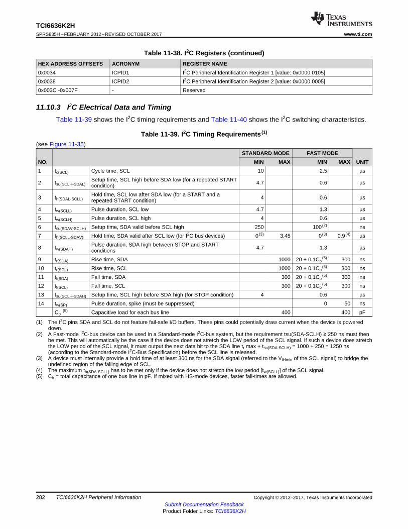
282
TCI6636K2HSPRS835H –FEBRUARY 2012–REVISED OCTOBER 2017 www.ti.com
Submit Documentation FeedbackProduct Folder Links: TCI6636K2H
TCI6636K2H Peripheral Information Copyright © 2012–2017, Texas Instruments Incorporated
Table 11-38. I2C Registers (continued)HEX ADDRESS OFFSETS ACRONYM REGISTER NAME0x0034 ICPID1 I2C Peripheral Identification Register 1 [value: 0x0000 0105]0x0038 ICPID2 I2C Peripheral Identification Register 2 [value: 0x0000 0005]0x003C -0x007F - Reserved
11.10.3 I2C Electrical Data and TimingTable 11-39 shows the I2C timing requirements and Table 11-40 shows the I2C switching characteristics.
(1) The I2C pins SDA and SCL do not feature fail-safe I/O buffers. These pins could potentially draw current when the device is powereddown.
(2) A Fast-mode I2C-bus device can be used in a Standard-mode I2C-bus system, but the requirement tsu(SDA-SCLH) ≥ 250 ns must thenbe met. This will automatically be the case if the device does not stretch the LOW period of the SCL signal. If such a device does stretchthe LOW period of the SCL signal, it must output the next data bit to the SDA line tr max + tsu(SDA-SCLH) = 1000 + 250 = 1250 ns(according to the Standard-mode I2C-Bus Specification) before the SCL line is released.
(3) A device must internally provide a hold time of at least 300 ns for the SDA signal (referred to the VIHmin of the SCL signal) to bridge theundefined region of the falling edge of SCL.
(4) The maximum th(SDA-SCLL) has to be met only if the device does not stretch the low period [tw(SCLL)] of the SCL signal.(5) Cb = total capacitance of one bus line in pF. If mixed with HS-mode devices, faster fall-times are allowed.
Table 11-39. I2C Timing Requirements (1)
(see Figure 11-35)
NO.STANDARD MODE FAST MODE
UNITMIN MAX MIN MAX1 tc(SCL) Cycle time, SCL 10 2.5 µs
2 tsu(SCLH-SDAL)Setup time, SCL high before SDA low (for a repeated STARTcondition) 4.7 0.6 µs
3 th(SDAL-SCLL)Hold time, SCL low after SDA low (for a START and arepeated START condition) 4 0.6 µs
4 tw(SCLL) Pulse duration, SCL low 4.7 1.3 µs5 tw(SCLH) Pulse duration, SCL high 4 0.6 µs6 tsu(SDAV-SCLH) Setup time, SDA valid before SCL high 250 100 (2) ns7 th(SCLL-SDAV) Hold time, SDA valid after SCL low (for I2C bus devices) 0 (3) 3.45 0 (3) 0.9 (4) µs
8 tw(SDAH)Pulse duration, SDA high between STOP and STARTconditions 4.7 1.3 µs
9 tr(SDA) Rise time, SDA 1000 20 + 0.1Cb(5) 300 ns
10 tr(SCL) Rise time, SCL 1000 20 + 0.1Cb(5) 300 ns
11 tf(SDA) Fall time, SDA 300 20 + 0.1Cb(5) 300 ns
12 tf(SCL) Fall time, SCL 300 20 + 0.1Cb(5) 300 ns
13 tsu(SCLH-SDAH) Setup time, SCL high before SDA high (for STOP condition) 4 0.6 µs14 tw(SP) Pulse duration, spike (must be suppressed) 0 50 ns
Cb(5) Capacitive load for each bus line 400 400 pF

10
8
4
37
12
5
6 14
2
3
13
Stop Start RepeatedStart
Stop
SDA
SCL
1
11 9
283
TCI6636K2Hwww.ti.com SPRS835H –FEBRUARY 2012–REVISED OCTOBER 2017
Submit Documentation FeedbackProduct Folder Links: TCI6636K2H
TCI6636K2H Peripheral InformationCopyright © 2012–2017, Texas Instruments Incorporated
(1) Cb = total capacitance of one bus line in pF. If mixed with HS-mode devices, faster fall-times are allowed.
Figure 11-35. I2C Receive Timings
Table 11-40. I2C Switching Characteristics (1)
(see Figure 11-36)
NO. PARAMETER
STANDARDMODE FAST MODE
UNITMIN MAX MIN MAX16 tc(SCL) Cycle time, SCL 10 2.5 µs
17 tsu(SCLH-SDAL)Setup time, SCL high to SDA low (for a repeated STARTcondition) 4.7 0.6 µs
18 th(SDAL-SCLL)Hold time, SDA low after SCL low (for a START and a repeatedSTART condition) 4 0.6 µs
19 tw(SCLL) Pulse duration, SCL low 4.7 1.3 µs20 tw(SCLH) Pulse duration, SCL high 4 0.6 µs21 td(SDAV-SDLH) Delay time, SDA valid to SCL high 250 100 ns22 tv(SDLL-SDAV) Valid time, SDA valid after SCL low (for I2C bus devices) 0 0 0.9 µs
23 tw(SDAH)Pulse duration, SDA high between STOP and STARTconditions 4.7 1.3 µs
24 tr(SDA) Rise time, SDA 1000 20 + 0.1Cb(1) 300 ns
25 tr(SCL) Rise time, SCL 1000 20 + 0.1Cb(1) 300 ns
26 tf(SDA) Fall time, SDA 300 20 + 0.1Cb(1) 300 ns
27 tf(SCL) Fall time, SCL 300 20 + 0.1Cb(1) 300 ns
28 td(SCLH-SDAH) Delay time, SCL high to SDA high (for STOP condition) 4 0.6 µsCp Capacitance for each I2C pin 10 10 pF

25
23
19
18
22
27
20
21
17
18
28
Stop Start RepeatedStart
Stop
SDA
SCL
16
26 24
284
TCI6636K2HSPRS835H –FEBRUARY 2012–REVISED OCTOBER 2017 www.ti.com
Submit Documentation FeedbackProduct Folder Links: TCI6636K2H
TCI6636K2H Peripheral Information Copyright © 2012–2017, Texas Instruments Incorporated
Figure 11-36. I2C Transmit Timings
11.11 SPI PeripheralThe Serial Peripheral Interconnect (SPI) module provides an interface between the SoC and other SPI-compliant devices. The primary intent of this interface is to allow for connection to an SPI ROM for boot.The SPI module on TCI6636K2H is supported only in master mode. Additional chip-level components canalso be included, such as temperature sensors or an I/O expander.
11.11.1 SPI Electrical Data and TimingTable 11-41 shows the SPI timing requirements and Table 11-42 shows the SPI switching characteristics.
Table 11-41. SPI Timing Requirements(see Figure 11-37)NO. MIN MAX UNIT
Master Mode Timing Diagrams — Base Timings for 3 Pin Mode7 tsu(SPIDIN-SPC) Input setup time, SPIDIN valid before receive edge of SPICLK. Polarity = 0 Phase = 0 2 ns7 tsu(SPIDIN-SPC) Input setup time, SPIDIN valid before receive edge of SPICLK. Polarity = 0 Phase = 1 2 ns7 tsu(SPIDIN-SPC) Input setup time, SPIDIN valid before receive edge of SPICLK. Polarity = 1 Phase = 0 2 ns7 tsu(SPIDIN-SPC) Input setup time, SPIDIN valid before receive edge of SPICLK. Polarity = 1 Phase = 1 2 ns8 th(SPC-SPIDIN) Input hold time, SPIDIN valid after receive edge of SPICLK. Polarity = 0 Phase = 0 5 ns8 th(SPC-SPIDIN) Input hold time, SPIDIN valid after receive edge of SPICLK. Polarity = 0 Phase = 1 5 ns8 th(SPC-SPIDIN) Input hold time, SPIDIN valid after receive edge of SPICLK. Polarity = 1 Phase = 0 5 ns8 th(SPC-SPIDIN) Input hold time, SPIDIN valid after receive edge of SPICLK. Polarity = 1 Phase = 1 5 ns
(1) P2=1/(SYSCLK1/6)
Table 11-42. SPI Switching Characteristics(see Figure 11-37 and Figure 11-38)NO. PARAMETER MIN MAX UNIT
Master Mode Timing Diagrams — Base Timings for 3 Pin Mode1 tc(SPC) Cycle time, SPICLK, all master modes 3*P2 (1) ns2 tw(SPCH) Pulse width high, SPICLK, all master modes 0.5*(3*P2) – 1 ns3 tw(SPCL) Pulse width low, SPICLK, all master modes 0.5*(3*P2) – 1 ns
4 td(SPIDOUT-SPC) Setup (Delay), initial data bit valid on SPIDOUT toinitial edge on SPICLK. Polarity = 0, Phase = 0. 5 ns
4 td(SPIDOUT-SPC) Setup (Delay), initial data bit valid on SPIDOUT toinitial edge on SPICLK. Polarity = 0, Phase = 1. 5 ns

285
TCI6636K2Hwww.ti.com SPRS835H –FEBRUARY 2012–REVISED OCTOBER 2017
Submit Documentation FeedbackProduct Folder Links: TCI6636K2H
TCI6636K2H Peripheral InformationCopyright © 2012–2017, Texas Instruments Incorporated
Table 11-42. SPI Switching Characteristics (continued)(see Figure 11-37 and Figure 11-38)NO. PARAMETER MIN MAX UNIT
4 td(SPIDOUT-SPC) Setup (Delay), initial data bit valid on SPIDOUT toinitial edge on SPICLK Polarity = 1, Phase = 0 5 ns
4 td(SPIDOUT-SPC) Setup (Delay), initial data bit valid on SPIDOUT toinitial edge on SPICLK Polarity = 1, Phase = 1 5 ns
5 td(SPC-SPIDOUT)Setup (Delay), subsequent data bits valid onSPIDOUT to initial edge on SPICLK. Polarity = 0Phase = 0
2 ns
5 td(SPC-SPIDOUT)Setup (Delay), subsequent data bits valid onSPIDOUT to initial edge on SPICLK Polarity = 0Phase = 1
2 ns
5 td(SPC-SPIDOUT)Setup (Delay), subsequent data bits valid onSPIDOUT to initial edge on SPICLK Polarity = 1Phase = 0
2 ns
5 td(SPC-SPIDOUT)Setup (Delay), subsequent data bits valid onSPIDOUT to initial edge on SPICLK Polarity = 1Phase = 1
2 ns
6 toh(SPC-SPIDOUT)Output hold time, SPIDOUT valid after receiveedge of SPICLK except for final bit. Polarity = 0Phase = 0
0.5*tc – 2 ns
6 toh(SPC-SPIDOUT)Output hold time, SPIDOUT valid after receiveedge of SPICLK except for final bit. Polarity = 0Phase = 1
0.5*tc – 2 ns
6 toh(SPC-SPIDOUT)Output hold time, SPIDOUT valid after receiveedge of SPICLK except for final bit. Polarity = 1Phase = 0
0.5*tc – 2 ns
6 toh(SPC-SPIDOUT)Output hold time, SPIDOUT valid after receiveedge of SPICLK except for final bit. Polarity = 1Phase = 1
0.5*tc – 2 ns
Additional SPI Master Timings — 4 Pin Mode with Chip Select Option
19 td(SCS-SPC) Delay from SPISCSx\ active to first SPICLK.Polarity = 0 Phase = 0 2*P2 – 5 2*P2 + 5 ns
19 td(SCS-SPC) Delay from SPISCSx\ active to first SPICLK.Polarity = 0 Phase = 1
0.5*tc + (2*P2) –5 0.5*tc + (2*P2) + 5 ns
19 td(SCS-SPC) Delay from SPISCSx\ active to first SPICLK.Polarity = 1 Phase = 0 2*P2 – 5 2*P2 + 5 ns
19 td(SCS-SPC) Delay from SPISCSx\ active to first SPICLK.Polarity = 1 Phase = 1
0.5*tc + (2*P2) –5 0.5*tc + (2*P2) + 5 ns
20 td(SPC-SCS) Delay from final SPICLK edge to masterdeasserting SPISCSx\. Polarity = 0 Phase = 0 1*P2 – 5 1*P2 + 5 ns
20 td(SPC-SCS) Delay from final SPICLK edge to masterdeasserting SPISCSx\. Polarity = 0 Phase = 1
0.5*tc + (1*P2) –5 0.5*tc + (1*P2) + 5 ns
20 td(SPC-SCS) Delay from final SPICLK edge to masterdeasserting SPISCSx\. Polarity = 1 Phase = 0 1*P2 – 5 1*P2 + 5 ns
20 td(SPC-SCS) Delay from final SPICLK edge to masterdeasserting SPISCSx\. Polarity = 1 Phase = 1
0.5*tc + (1*P2) –5 0.5*tc + (1*P2) + 5 ns
tw(SCSH)Minimum inactive time on SPISCSx\ pin betweentwo transfers when SPISCSx\ is not held using theCSHOLD feature.
2*P2 – 5 ns

MASTER MODE 4 PIN WITH CHIP SELECT
SPICLK
SPIDOUT
SPIDIN
SPISCSx
MO(0) MO(1) MO(n−1) MO(n)
MI(0) MI(1) MI(n−1) MI(n)
19 20
SPICLK
SPIDOUT
SPIDIN
MO(0) MO(1) MO(n−1) MO(n)
MI(0) MI(1) MI(n−1) MI(n)
MO(0) MO(1) MO(n−1) MO(n)
MI(0) MI(1) MI(n−1) MI(n)
MO(0) MO(1) MO(n−1) MO(n)
MI(0) MI(1) MI(n−1) MI(n)
MO(0) MO(1) MO(n−1) MO(n)
MI(0) MI(1) MI(n−1) MI(n)
6
6
7
7
7
7
8
8
8
8
32
6
1
4
4
4
4 5
5
5 6
MASTER MODE
POLARITY = 0 PHASE = 0
MASTER MODE
POLARITY = 0 PHASE = 1
MASTER MODE
POLARITY = 1 PHASE = 0
MASTER MODE
POLARITY = 1 PHASE = 1
5
SPICLK
SPIDOUT
SPIDIN
SPICLK
SPIDOUT
SPIDIN
SPICLK
SPIDOUT
SPIDIN
286
TCI6636K2HSPRS835H –FEBRUARY 2012–REVISED OCTOBER 2017 www.ti.com
Submit Documentation FeedbackProduct Folder Links: TCI6636K2H
TCI6636K2H Peripheral Information Copyright © 2012–2017, Texas Instruments Incorporated
Figure 11-37. SPI Master Mode Timing Diagrams — Base Timings for 3-Pin Mode
Figure 11-38. SPI Additional Timings for 4-Pin Master Mode with Chip Select Option

287
TCI6636K2Hwww.ti.com SPRS835H –FEBRUARY 2012–REVISED OCTOBER 2017
Submit Documentation FeedbackProduct Folder Links: TCI6636K2H
TCI6636K2H Peripheral InformationCopyright © 2012–2017, Texas Instruments Incorporated
11.12 HyperLink PeripheralThe TCI6636K2H includes HyperLinks for companion device interfaces. This is a four-lane SerDesinterface designed to operate at up to 10 Gbps per lane from pin-to-pin. The interface is used to connectwith external accelerators that are manufactured using TI libraries. The HyperLink lines must beconnected with DC coupling.
The interface includes the serial station management interfaces used to send power management andflow messages between devices. Each HyperLink interface consists of four LVCMOS inputs and fourLVCMOS outputs configured as two 2-wire input buses and two 2-wire output buses. Each 2-wire busincludes a data signal and a clock signal.
Table 11-43 shows the Hyperlink timing requirements and Table 11-44 shows the Hyperlink switchingcharacteristics.
Table 11-43. HyperLink Peripheral Timing Requirements(see Figure 11-39, Figure 11-40, and Figure 11-41)NO. MIN MAX UNIT
FL Interface
1 tc(HYPTXFLCLK) Clock period – HYPTXFLCLK (C1) 5.75 ns
2 tw(HYPTXFLCLKH) High pulse width – HYPTXFLCLK 0.4*C1 0.6*C1 ns
3 tw(HYPTXFLCLKL) Low pulse width – HYPTXFLCLK 0.4*C1 0.6*C1 ns
6 tsu(HYPTXFLDAT-HYPTXFLCLKH) Setup time – HYPTXFLDAT valid beforeHYPTXFLCLK high 1 ns
7 th(HYPTXFLCLKH-HYPTXFLDAT) Hold time – HYPTXFLDAT valid afterHYPTXFLCLK high 1 ns
6 tsu(HYPTXFLDAT-HYPTXFLCLKL) Setup time – HYPTXFLDAT valid beforeHYPTXFLCLK low 1 ns
7 th(HYPTXFLCLKL-HYPTXFLDAT) Hold time – HYPTXFLDAT valid afterHYPTXFLCLK low 1 ns
PM Interface
1 tc(HYPRXPMCLK) Clock period – HYPRXPMCLK (C3) 5.75 ns
2 tw(HYPRXPMCLK) High pulse width – HYPRXPMCLK 0.4*C3 0.6*C3 ns
3 tw(HYPRXPMCLK) Low pulse width – HYPRXPMCLK 0.4*C3 0.6*C3 ns
6 tsu(HYPRXPMDAT-HYPRXPMCLKH) Setup time – HYPRXPMDAT valid beforeHYPRXPMCLK high 1 ns
7 th(HYPRXPMCLKH-HYPRXPMDAT) Hold time – HYPRXPMDAT valid afterHYPRXPMCLK high 1 ns
6 tsu(HYPRXPMDAT-HYPRXPMCLKL) Setup time – HYPRXPMDAT valid beforeHYPRXPMCLK low 1 ns
7 th(HYPRXPMCLKL-HYPRXPMDAT) Hold time – HYPRXPMDAT valid afterHYPRXPMCLK low 1 ns
Table 11-44. HyperLink Peripheral Switching Characteristics(see Figure 11-39, Figure 11-40, and Figure 11-41)NO. PARAMETER MIN MAX UNIT
FL Interface
1 tc(HYPRXFLCLK) Clock period – HYPRXFLCLK (C2) 6.4 ns
2 tw(HYPRXFLCLKH) High pulse width – HYPRXFLCLK 0.4*C2 0.6*C2 ns
3 tw(HYPRXFLCLKL) Low pulse width – HYPRXFLCLK 0.4*C2 0.6*C2 ns
4 tosu(HYPRXFLDAT-HYPRXFLCLKH) Setup time – HYPRXFLDAT valid beforeHYPRXFLCLK high 0.25*C2-0.4 ns
5 toh(HYPRXFLCLKH-HYPRXFLDAT) Hold time – HYPRXFLDAT valid afterHYPRXFLCLK high 0.25*C2-0.4 ns
4 tosu(HYPRXFLDAT-HYPRXFLCLKL) Setup time – HYPRXFLDAT valid beforeHYPRXFLCLK low 0.25*C2-0.4 ns
5 toh(HYPRXFLCLKL-HYPRXFLDAT) Hold time – HYPRXFLDAT valid afterHYPRXFLCLK low 0.25*C2-0.4 ns
PM Interface

7676
HYPRX<xx>CLK
HYPRX<xx>DAT
5454
HYPTX<xx>CLK
HYPTX<xx>DAT
2 3
1
288
TCI6636K2HSPRS835H –FEBRUARY 2012–REVISED OCTOBER 2017 www.ti.com
Submit Documentation FeedbackProduct Folder Links: TCI6636K2H
TCI6636K2H Peripheral Information Copyright © 2012–2017, Texas Instruments Incorporated
Table 11-44. HyperLink Peripheral Switching Characteristics (continued)(see Figure 11-39, Figure 11-40, and Figure 11-41)NO. PARAMETER MIN MAX UNIT
1 tc(HYPTXPMCLK) Clock period – HYPTXPMCLK (C4) 6.4 ns
2 tw(HYPTXPMCLK) High pulse width – HYPTXPMCLK 0.4*C4 0.6*C4 ns
3 tw(HYPTXPMCLK) Low pulse width – HYPTXPMCLK 0.4*C4 0.6*C4 ns
4 tosu(HYPTXPMDAT-HYPTXPMCLKH) Setup time – HYPTXPMDAT valid beforeHYPTXPMCLK high 0.25*C2-0.4 ns
5 toh(HYPTXPMCLKH-HYPTXPMDAT) Hold time – HYPTXPMDAT valid afterHYPTXPMCLK high 0.25*C2-0.4 ns
4 tosu(HYPTXPMDAT-HYPTXPMCLKL) Setup time – HYPTXPMDAT valid beforeHYPTXPMCLK low 0.25*C2-0.4 ns
5 toh(HYPTXPMCLKL-HYPTXPMDAT) Hold time – HYPTXPMDAT valid afterHYPTXPMCLK low 0.25*C2-0.4 ns
Figure 11-39. HyperLink Station Management Clock Timing
<xx> represents the interface that is being used: PM or FL
Figure 11-40. HyperLink Station Management Transmit Timing
<xx> represents the interface that is being used: PM or FL
Figure 11-41. HyperLink Station Management Receive Timing

8
TXD Bit N-1 Bit N Stop Start Bit 0
CTS
6554
Stop/IdleRXD Start Bit 0 Bit 1 Bit N-1 Bit N Parity Stop Idle Start
289
TCI6636K2Hwww.ti.com SPRS835H –FEBRUARY 2012–REVISED OCTOBER 2017
Submit Documentation FeedbackProduct Folder Links: TCI6636K2H
TCI6636K2H Peripheral InformationCopyright © 2012–2017, Texas Instruments Incorporated
11.13 UART PeripheralThe universal asynchronous receiver/transmitter (UART) module provides an interface between the deviceand a UART terminal interface or other UART-based peripheral. The UART is based on the industrystandard TL16C550 asynchronous communications element which, in turn, is a functional upgrade of theTL16C450. Functionally similar to the TL16C450 on power up (single character or TL16C450 mode), theUART can be placed in an alternate FIFO (TL16C550) mode. This relieves the SoC of excessive softwareoverhead by buffering received and transmitted characters. The receiver and transmitter FIFOs store up to16 bytes including three additional bits of error status per byte for the receiver FIFO.
The UART performs serial-to-parallel conversions on data received from a peripheral device and parallel-to-serial conversion on data received from the C66x CorePac to be sent to the peripheral device. TheC66x CorePac can read the UART status at any time. The UART includes control capability and aprocessor interrupt system that can be tailored to minimize software management of the communicationslink. For more information on UART, see the KeyStone Architecture Universal AsynchronousReceiver/Transmitter (UART) User's Guide.
Table 11-45 shows the UART timing requirements and Table 11-46 shows the UART switchingcharacteristics.
(1) U = UART baud time = 1/programmed baud rate(2) P = 1/(SYSCLK1/6)
Table 11-45. UART Timing Requirements(see Figure 11-42 and Figure 11-43)NO. MIN MAX UNIT
Receive Timing4 tw(RXSTART) Pulse width, receive start bit 0.96U (1) 1.05U ns5 tw(RXH) Pulse width, receive data/parity bit high 0.96U 1.05U ns5 tw(RXL) Pulse width, receive data/parity bit low 0.96U 1.05U ns6 tw(RXSTOP1) Pulse width, receive stop bit 1 0.96U 1.05U ns6 tw(RXSTOP15) Pulse width, receive stop bit 1.5 0.96U 1.05U ns6 tw(RXSTOP2) Pulse width, receive stop bit 2 0.96U 1.05U ns
Autoflow Timing Requirements8 td(CTSL-TX) Delay time, CTS asserted to START bit transmit P (2) 5P ns
Figure 11-42. UART Receive Timing Waveform
Figure 11-43. UART CTS (Clear-to-Send Input) — Autoflow Timing Waveform
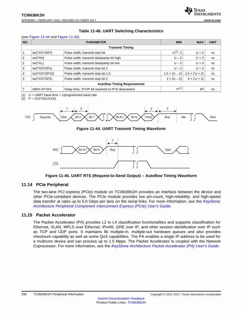
7
RXD Bit N-1 Bit N Stop Start
CTS
3221
Stop/IdleTXD Start Bit 0 Bit 1 Bit N-1 Bit N Parity Stop Idle Start
290
TCI6636K2HSPRS835H –FEBRUARY 2012–REVISED OCTOBER 2017 www.ti.com
Submit Documentation FeedbackProduct Folder Links: TCI6636K2H
TCI6636K2H Peripheral Information Copyright © 2012–2017, Texas Instruments Incorporated
(1) U = UART baud time = 1/programmed baud rate(2) P = 1/(SYSCLK1/6)
Table 11-46. UART Switching Characteristics(see Figure 11-44 and Figure 11-45)NO. PARAMETER MIN MAX UNIT
Transmit Timing1 tw(TXSTART) Pulse width, transmit start bit U (1)- 2 U + 2 ns2 tw(TXH) Pulse width, transmit data/parity bit high U – 2 U + 2 ns2 tw(TXL) Pulse width, transmit data/parity bit low U – 2 U + 2 ns3 tw(TXSTOP1) Pulse width, transmit stop bit 1 U – 2 U + 2 ns3 tw(TXSTOP15) Pulse width, transmit stop bit 1.5 1.5 × (U – 2) 1.5 × ('U + 2) ns3 tw(TXSTOP2) Pulse width, transmit stop bit 2 2 × (U – 2) 2 × ('U + 2) ns
Autoflow Timing Requirements7 td(RX-RTSH) Delay time, STOP bit received to RTS deasserted P (2) 5P ns
Figure 11-44. UART Transmit Timing Waveform
Figure 11-45. UART RTS (Request-to-Send Output) – Autoflow Timing Waveform
11.14 PCIe PeripheralThe two-lane PCI express (PCIe) module on TCI6636K2H provides an interface between the device andother PCIe-compliant devices. The PCIe module provides low pin-count, high-reliability, and high-speeddata transfer at rates up to 5.0 Gbps per lane on the serial links. For more information, see the KeyStoneArchitecture Peripheral Component Interconnect Express (PCIe) User's Guide.
11.15 Packet AcceleratorThe Packet Accelerator (PA) provides L2 to L4 classification functionalities and supports classification forEthernet, VLAN, MPLS over Ethernet, IPv4/6, GRE over IP, and other session identification over IP suchas TCP and UDP ports. It maintains 8k multiple-in, multiple-out hardware queues and also provideschecksum capability as well as some QoS capabilities. The PA enables a single IP address to be used fora multicore device and can process up to 1.5 Mpps. The Packet Accelerator is coupled with the NetworkCoprocessor. For more information, see the KeyStone Architecture Packet Accelerator (PA) User’s Guide.
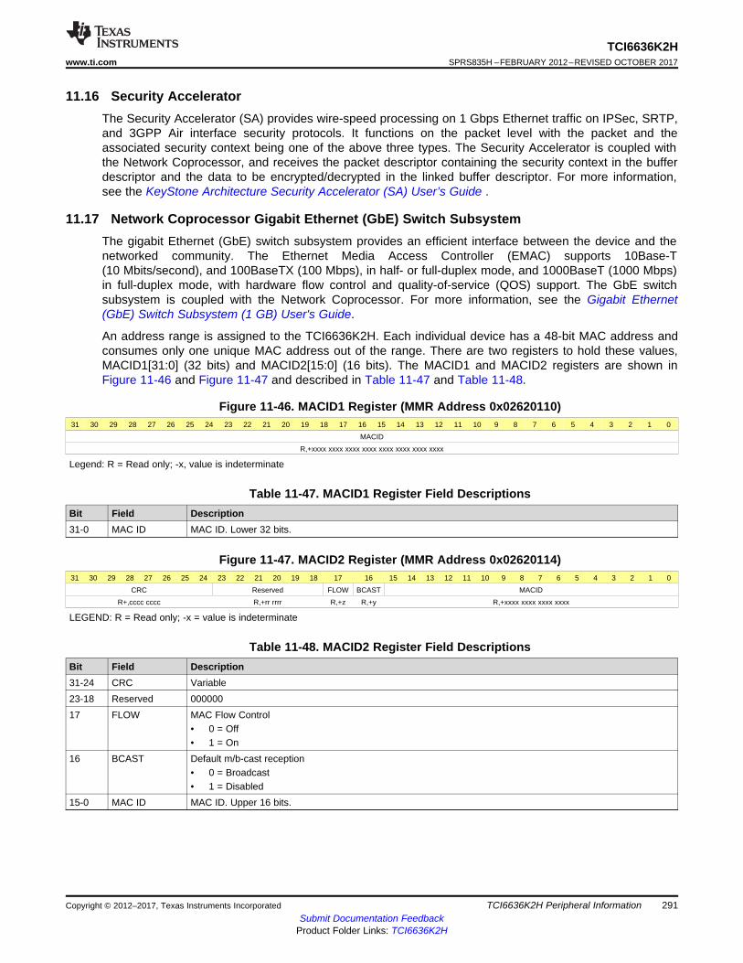
291
TCI6636K2Hwww.ti.com SPRS835H –FEBRUARY 2012–REVISED OCTOBER 2017
Submit Documentation FeedbackProduct Folder Links: TCI6636K2H
TCI6636K2H Peripheral InformationCopyright © 2012–2017, Texas Instruments Incorporated
11.16 Security AcceleratorThe Security Accelerator (SA) provides wire-speed processing on 1 Gbps Ethernet traffic on IPSec, SRTP,and 3GPP Air interface security protocols. It functions on the packet level with the packet and theassociated security context being one of the above three types. The Security Accelerator is coupled withthe Network Coprocessor, and receives the packet descriptor containing the security context in the bufferdescriptor and the data to be encrypted/decrypted in the linked buffer descriptor. For more information,see the KeyStone Architecture Security Accelerator (SA) User’s Guide .
11.17 Network Coprocessor Gigabit Ethernet (GbE) Switch SubsystemThe gigabit Ethernet (GbE) switch subsystem provides an efficient interface between the device and thenetworked community. The Ethernet Media Access Controller (EMAC) supports 10Base-T(10 Mbits/second), and 100BaseTX (100 Mbps), in half- or full-duplex mode, and 1000BaseT (1000 Mbps)in full-duplex mode, with hardware flow control and quality-of-service (QOS) support. The GbE switchsubsystem is coupled with the Network Coprocessor. For more information, see the Gigabit Ethernet(GbE) Switch Subsystem (1 GB) User's Guide.
An address range is assigned to the TCI6636K2H. Each individual device has a 48-bit MAC address andconsumes only one unique MAC address out of the range. There are two registers to hold these values,MACID1[31:0] (32 bits) and MACID2[15:0] (16 bits). The MACID1 and MACID2 registers are shown inFigure 11-46 and Figure 11-47 and described in Table 11-47 and Table 11-48.
Figure 11-46. MACID1 Register (MMR Address 0x02620110)31 30 29 28 27 26 25 24 23 22 21 20 19 18 17 16 15 14 13 12 11 10 9 8 7 6 5 4 3 2 1 0
MACID
R,+xxxx xxxx xxxx xxxx xxxx xxxx xxxx xxxx
Legend: R = Read only; -x, value is indeterminate
Table 11-47. MACID1 Register Field DescriptionsBit Field Description31-0 MAC ID MAC ID. Lower 32 bits.
Figure 11-47. MACID2 Register (MMR Address 0x02620114)31 30 29 28 27 26 25 24 23 22 21 20 19 18 17 16 15 14 13 12 11 10 9 8 7 6 5 4 3 2 1 0
CRC Reserved FLOW BCAST MACID
R+,cccc cccc R,+rr rrrr R,+z R,+y R,+xxxx xxxx xxxx xxxx
LEGEND: R = Read only; -x = value is indeterminate
Table 11-48. MACID2 Register Field DescriptionsBit Field Description31-24 CRC Variable23-18 Reserved 00000017 FLOW MAC Flow Control
• 0 = Off• 1 = On
16 BCAST Default m/b-cast reception• 0 = Broadcast• 1 = Disabled
15-0 MAC ID MAC ID. Upper 16 bits.
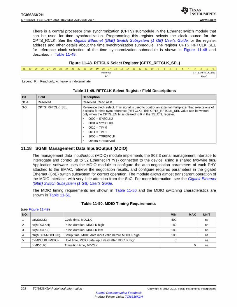
292
TCI6636K2HSPRS835H –FEBRUARY 2012–REVISED OCTOBER 2017 www.ti.com
Submit Documentation FeedbackProduct Folder Links: TCI6636K2H
TCI6636K2H Peripheral Information Copyright © 2012–2017, Texas Instruments Incorporated
There is a central processor time synchronization (CPTS) submodule in the Ethernet switch module thatcan be used for time synchronization. Programming this register selects the clock source for theCPTS_RCLK. See the Gigabit Ethernet (GbE) Switch Subsystem (1 GB) User's Guide for the registeraddress and other details about the time synchronization submodule. The register CPTS_RFTCLK_SELfor reference clock selection of the time synchronization submodule is shown in Figure 11-48 anddescribed in Table 11-49.
Figure 11-48. RFTCLK Select Register (CPTS_RFTCLK_SEL)31 30 29 28 27 26 25 24 23 22 21 20 19 18 17 16 15 14 13 12 11 10 9 8 7 6 5 4 3 2 1 0
Reserved CPTS_RFTCLK_SEL
R-0 RW-0
Legend: R = Read only; -x, value is indeterminate
Table 11-49. RFTCLK Select Register Field DescriptionsBit Field Description31-4 Reserved Reserved. Read as 0.3-0 CPTS_RFTCLK_SEL Reference clock select. This signal is used to control an external multiplexer that selects one of
8 clocks for time sync reference (RFTCLK). This CPTS_RFTCLK_SEL value can be writtenonly when the CPTS_EN bit is cleared to 0 in the TS_CTL register.• 0000 = SYSCLK2• 0001 = SYSCLK3• 0010 = TIMI0• 0011 = TIMI1• 1000 = TSREFCLK• Others = Reserved
11.18 SGMII Management Data Input/Output (MDIO)The management data input/output (MDIO) module implements the 802.3 serial management interface tointerrogate and control up to 32 Ethernet PHY(s) connected to the device, using a shared two-wire bus.Application software uses the MDIO module to configure the auto-negotiation parameters of each PHYattached to the EMAC, retrieve the negotiation results, and configure required parameters in the gigabitEthernet (GbE) switch subsystem for correct operation. The module allows almost transparent operation ofthe MDIO interface, with very little attention from the SoC. For more information, see the Gigabit Ethernet(GbE) Switch Subsystem (1 GB) User's Guide.
The MDIO timing requirements are shown in Table 11-50 and the MDIO switching characteristics areshown in Table 11-51.
Table 11-50. MDIO Timing Requirements(see Figure 11-49)NO. MIN MAX UNIT1 tc(MDCLK) Cycle time, MDCLK 400 ns2 tw(MDCLKH) Pulse duration, MDCLK high 180 ns3 tw(MDCLKL) Pulse duration, MDCLK low 180 ns4 tsu(MDIO-MDCLKH) Setup time, MDIO data input valid before MDCLK high 100 ns5 th(MDCLKH-MDIO) Hold time, MDIO data input valid after MDCLK high 0 ns
tt(MDCLK) Transition time, MDCLK 5 ns
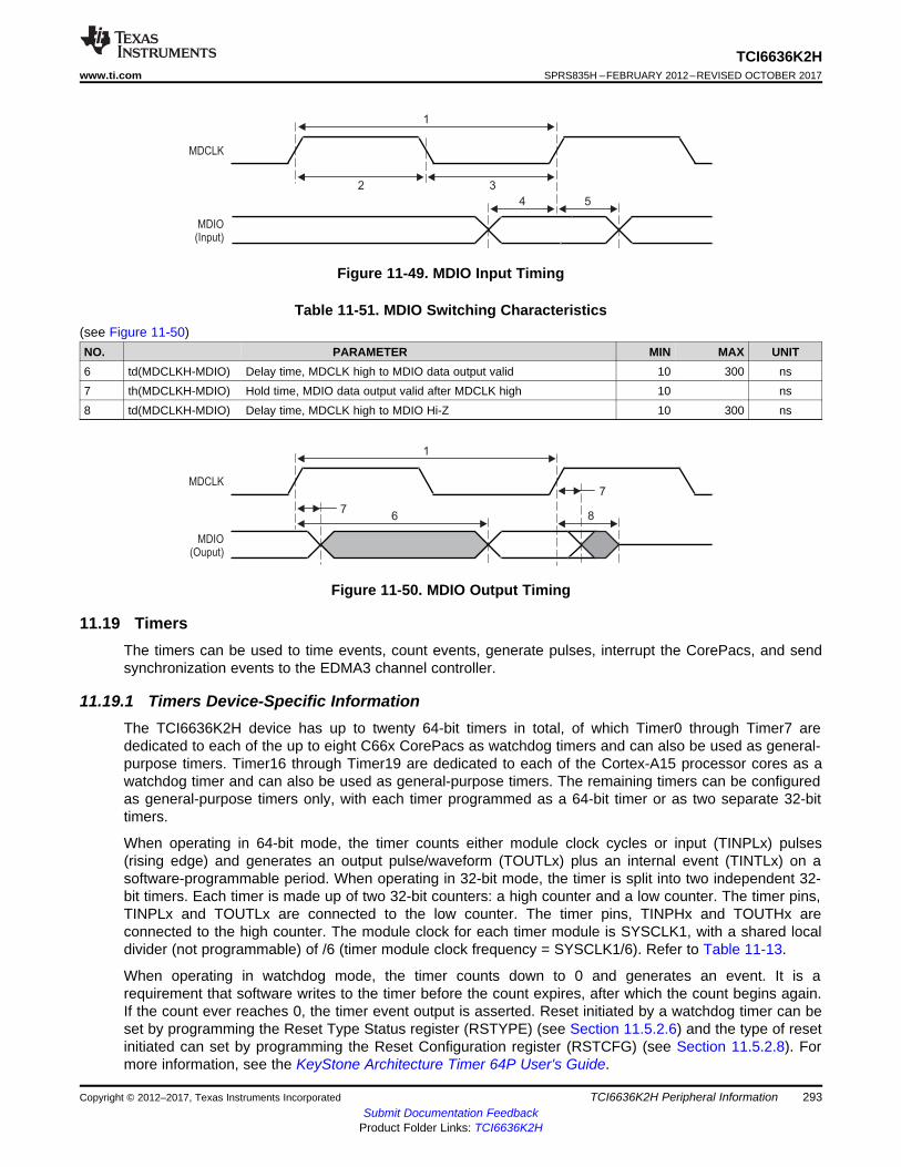
MDIO(Ouput)
1
6
MDCLK
8
7
7
MDIO(Input)
5
1
4
MDCLK
2 3
293
TCI6636K2Hwww.ti.com SPRS835H –FEBRUARY 2012–REVISED OCTOBER 2017
Submit Documentation FeedbackProduct Folder Links: TCI6636K2H
TCI6636K2H Peripheral InformationCopyright © 2012–2017, Texas Instruments Incorporated
Figure 11-49. MDIO Input Timing
Table 11-51. MDIO Switching Characteristics(see Figure 11-50)NO. PARAMETER MIN MAX UNIT6 td(MDCLKH-MDIO) Delay time, MDCLK high to MDIO data output valid 10 300 ns7 th(MDCLKH-MDIO) Hold time, MDIO data output valid after MDCLK high 10 ns8 td(MDCLKH-MDIO) Delay time, MDCLK high to MDIO Hi-Z 10 300 ns
Figure 11-50. MDIO Output Timing
11.19 TimersThe timers can be used to time events, count events, generate pulses, interrupt the CorePacs, and sendsynchronization events to the EDMA3 channel controller.
11.19.1 Timers Device-Specific InformationThe TCI6636K2H device has up to twenty 64-bit timers in total, of which Timer0 through Timer7 arededicated to each of the up to eight C66x CorePacs as watchdog timers and can also be used as general-purpose timers. Timer16 through Timer19 are dedicated to each of the Cortex-A15 processor cores as awatchdog timer and can also be used as general-purpose timers. The remaining timers can be configuredas general-purpose timers only, with each timer programmed as a 64-bit timer or as two separate 32-bittimers.
When operating in 64-bit mode, the timer counts either module clock cycles or input (TINPLx) pulses(rising edge) and generates an output pulse/waveform (TOUTLx) plus an internal event (TINTLx) on asoftware-programmable period. When operating in 32-bit mode, the timer is split into two independent 32-bit timers. Each timer is made up of two 32-bit counters: a high counter and a low counter. The timer pins,TINPLx and TOUTLx are connected to the low counter. The timer pins, TINPHx and TOUTHx areconnected to the high counter. The module clock for each timer module is SYSCLK1, with a shared localdivider (not programmable) of /6 (timer module clock frequency = SYSCLK1/6). Refer to Table 11-13.
When operating in watchdog mode, the timer counts down to 0 and generates an event. It is arequirement that software writes to the timer before the count expires, after which the count begins again.If the count ever reaches 0, the timer event output is asserted. Reset initiated by a watchdog timer can beset by programming the Reset Type Status register (RSTYPE) (see Section 11.5.2.6) and the type of resetinitiated can set by programming the Reset Configuration register (RSTCFG) (see Section 11.5.2.8). Formore information, see the KeyStone Architecture Timer 64P User's Guide.

TIMIx
1 2
TIMOx
3 4
294
TCI6636K2HSPRS835H –FEBRUARY 2012–REVISED OCTOBER 2017 www.ti.com
Submit Documentation FeedbackProduct Folder Links: TCI6636K2H
TCI6636K2H Peripheral Information Copyright © 2012–2017, Texas Instruments Incorporated
11.19.2 Timers Electrical Data and TimingTable 11-52 and Table 11-53 list timing requirements and switching characteristics of the timers.
(1) C = 1/SYSCLK1 clock frequency in ns
Table 11-52. Timer Input Timing Requirements (1)
(see Figure 11-51)NO. MIN MAX UNIT1 tw(TINPH) Pulse duration, high 12C ns2 tw(TINPL) Pulse duration, low 12C ns
(1) C = 1/SYSCLK1 clock frequency in ns.
Table 11-53. Timer Output Switching Characteristics (1)
(see Figure 11-51)NO. PARAMETER MIN MAX UNIT3 tw(TOUTH) Pulse duration, high 12C – 3 ns4 tw(TOUTL) Pulse duration, low 12C – 3 ns
Figure 11-51. Timer Timing
11.20 Rake Search Accelerator (RSA)There are sixteen Rake Search Accelerators (RSAs) on the device. Each C66x CorePac has one set ofdirectly-connected RSA pairs. The RSA is an extension of the C66x CorePac. The C66x CorePacperforms send/receive to the RSAs via the .L and .S functional units.
11.21 Enhanced Viterbi-Decoder Coprocessor (VCP2)The device has four high-performance embedded Viterbi Decoder Coprocessors (VCP2) that improvechannel-decoding operations on-chip. Operating at SYSCLK1 clock divided by 3, each VCP2 can decodemore than 762 12.2-Kbps 3G adaptive multi-rate (AMR) [K = 9, R = 1/3] voice channels when running at333 MHz. The VCP2 supports constraint lengths K = 5, 6, 7, 8, and 9, rates R = 3/4, 1/2, 1/3, 1/4, and 1/5,and flexible polynomials, while generating hard decisions or soft decisions. Communications between theVCP2 and the C66x CorePac are carried out through the EDMA3 controller. The VCP2 supports:• Unlimited frame sizes• Code rates 3/4, 1/2, 1/3, 1/4, and 1/5• Constraint lengths 5, 6, 7, 8, and 9• Programmable encoder polynomials• Programmable reliability and convergence lengths• Hard and soft decoded decisions• Tail and convergent modes• Yamamoto logic• Tail-biting logic• Various input and output FIFO lengths
For more information, see the KeyStone Architecture Viterbi Coprocessor (VCP2) User's Guide.

295
TCI6636K2Hwww.ti.com SPRS835H –FEBRUARY 2012–REVISED OCTOBER 2017
Submit Documentation FeedbackProduct Folder Links: TCI6636K2H
TCI6636K2H Peripheral InformationCopyright © 2012–2017, Texas Instruments Incorporated
11.22 Turbo Decoder Coprocessor (TCP3d)The TCI6636K2H has two high-performance embedded Turbo-Decoder Coprocessors (TCP3d) that speedup channel-decoding operations on-chip for WCDMA, HSPA, HSPA+, TD-SCDMA, LTE, and WiMAX.Operating at SYSCLK1 divided by 2 or 3, the TCP3d processes data channels at a throughputof > 100 Mbps. For more information, see the KeyStone Architecture Turbo Decoder Coprocessor 3(TCP3d) User's Guide.
11.23 Turbo Encoder Coprocessor (TCP3e)The TCI6636K2H has a high-performance Turbo-Encoder Coprocessor (TCP3e) (embedded in the BCP)that speeds up channel-encoding operations on-chip for WCDMA, HSPA, HSPA+, TD-SCDMA, LTE, andWiMAX. Operating at SYSCLK1 divided by 3, the TCP3e is capable of processing data channels at athroughput of > 200 Mbps. For more information, see the KeyStone Architecture Turbo EncoderCoprocessor 3 (TCP3e) User's Guide.
11.24 Bit Rate Coprocessor (BCP)The BCP is a hardware accelerator for wireless infrastructure and performs most of the uplink anddownlink layer 1 bit processing for 3G and 4G wireless standards. BCP supports LTE, LTE-A, FDDWCDMA, TD-SCDMA, and WiMAX 802.16-2009 standards. It supports various downlink processingblocks like CRC attachment, turbo encoding, rate matching, code block concatenation, scrambling, andmodulation. BCP supports various uplink processing blocks like soft slicer, de-scrambler, de-concatenation, rate de-matching, and LLR combining. For more information, see the KeyStoneArchitecture Bit Rate Coprocessor (BCP) User's Guide.
11.25 Serial RapidIO (SRIO) PortThe SRIO port on the device is a high-performance, low pin-count SerDes interconnect. SRIOinterconnects in a baseband board design provide connectivity and control among the components. Thedevice supports four 1× Serial RapidIO links or one 4× Serial RapidIO link. The SRIO interface is designedto operate at a data rate of up to 5 Gbps per differential pair. This equals 20 raw GBaud/s for the 4× SRIOport, or approximately 15 Gbps data throughput rate.
The PHY part of the SRIO consists of the physical layer and includes the input and output buffers (eachserial link consists of a differential pair), the 8-bit/10-bit encoder/decoder, the PLL clock recovery, and theparallel-to-serial/serial-to-parallel converters.
For more information, see the KeyStone Architecture Serial RapidIO (SRIO) User's Guide.
11.25.1 Serial RapidIO Device-Specific InformationThe approach to specifying interface timing for the SRIO Port is different from other interfaces. For theseother interfaces, the device timing was specified in terms of data manual specifications and I/O bufferinformation specification (IBIS) models.
The Serial RapidIO peripheral is a master peripheral in the device. It conforms to the RapidIO™Interconnect Specification, Part VI: Physical Layer 1×/4× LP-Serial Specification, Revision 1.3.
For the SRIO port, Texas Instruments provides a PCB solution showing two TI SRIO-enabled DSPsconnected together via a 4× SRIO link. TI has performed the simulation and system characterization toensure all SRIO interface timings in this solution are met.
NOTETI supports only designs that follow the board design guidelines outlined in the RapidIO™Interconnect Specification, Part VI: Physical Layer 1×/4× LP-Serial Specification, Revision1.3.

296
TCI6636K2HSPRS835H –FEBRUARY 2012–REVISED OCTOBER 2017 www.ti.com
Submit Documentation FeedbackProduct Folder Links: TCI6636K2H
TCI6636K2H Peripheral Information Copyright © 2012–2017, Texas Instruments Incorporated
11.26 General-Purpose Input/Output (GPIO)
11.26.1 GPIO Device-Specific InformationThe GPIO peripheral pins are used for general-purpose input/output for the device. These pins are alsoused to configure the device at boot time.
For more detailed information on device/ and peripheral configuration and the TCI6636K2H device pinmultiplexing, see Section 10.2.
These GPIO pins can also be used to generate individual core interrupts (no support of bank interrupt)and EDMA events.
11.26.2 GPIO Peripheral Register DescriptionTable 11-54 lists the GPIO registers.
Table 11-54. GPIO Registers
HEX ADDRESS OFFSETS ACRONYM REGISTER NAME0x0008 BINTEN GPIO interrupt per bank enable register0x000C - Reserved0x0010 DIR GPIO Direction Register0x0014 OUT_DATA GPIO Output Data Register0x0018 SET_DATA GPIO Set Data Register0x001C CLR_DATA GPIO Clear Data Register0x0020 IN_DATA GPIO Input Data Register0x0024 SET_RIS_TRIG GPIO Set Rising Edge Interrupt Register0x0028 CLR_RIS_TRIG GPIO Clear Rising Edge Interrupt Register0x002C SET_FAL_TRIG GPIO Set Falling Edge Interrupt Register0x0030 CLR_FAL_TRIG GPIO Clear Falling Edge Interrupt Register0x008C - Reserved0x0090 – 0x03FF - Reserved
11.26.3 GPIO Electrical Data and TimingThe GPIO input timing requirements are shown in Table 11-55 and the GPIO output switchingcharacteristics are shown in Table 11-56.
(1) C = 1/SYSCLK1 clock frequency in ns
Table 11-55. GPIO Input Timing Requirements (1)
(see Figure 11-52)NO. MIN MAX UNIT1 tw(GPOH) Pulse duration, GPOx high 12C ns2 tw(GPOL) Pulse duration, GPOx low 12C ns
(1) C = 1/SYSCLK1 clock frequency in ns
Table 11-56. GPIO Output Switching Characteristics (1)
(see Figure 11-52)NO. PARAMETER MIN MAX UNIT3 tw(GPOH) Pulse duration, GPOx high 36C – 8 ns4 tw(GPOL) Pulse duration, GPOx low 36C – 8 ns

GPIx
1 2
GPOx
3 4
297
TCI6636K2Hwww.ti.com SPRS835H –FEBRUARY 2012–REVISED OCTOBER 2017
Submit Documentation FeedbackProduct Folder Links: TCI6636K2H
TCI6636K2H Peripheral InformationCopyright © 2012–2017, Texas Instruments Incorporated
Figure 11-52. GPIO Timing
11.27 Semaphore2The device contains an enhanced Semaphore module for the management of shared resources of theSoC. The Semaphore enforces atomic accesses to shared chip-level resources so that the read-modify-write sequence is not broken. The Semaphore module has unique interrupts to each of the CorePacs toidentify when that CorePac has acquired the resource.
Semaphore resources within the module are not tied to specific hardware resources. It is a softwarerequirement to allocate semaphore resources to the hardware resources to be arbitrated.
The Semaphore module supports all the CPUs in the device—12 for 66AK2H14 and 66AK2H12 devices,and 6 for 66AK2H06 devices—and contains 64 semaphores that can be shared within the system.
There are two methods of accessing a semaphore resource:• Direct Access: A C66x CorePac directly accesses a semaphore resource. If free, the semaphore is
granted. If not free, the semaphore is not granted.• Indirect Access: A C66x CorePac indirectly accesses a semaphore resource by writing to it. Once the
resource is free, an interrupt notifies the C66x CorePac that the resource is available.
11.28 Antenna Interface Subsystem 2 (AIF2)The AIF2 transfers data between the external RF units and the C66x CorePacs, RAC, TAC, and the FFTCmodules via the TeraNet. The external AIF2 interface connects the AIF2 with either RF units and/or otherbaseband OBSAI/CPRI devices. The AIF2 has 11 timer synchronization events from the AIF2 Timer (AT)module:• Timer synchronization events 0-3 are routed as primary events to the EDMA3CC1 and also as
secondary events to the C66x CorePacs via CIC2.• Timer synchronization events 3-7 are routed as primary events to the EDMA3CC2.• Timer synchronization events 8, 9, 10, 11 and 12 are hard-wired to TAC, RAC_0, RAC_1, RAC_2 and
RAC_3 respectively.
AIF2 timing requirements are shown in Table 11-57 and AIF2 switching characteristics are shown inTable 11-58.
(1) C1 = tc(RP1CLKN/P)
Table 11-57. AIF2 Timer Module Timing Requirements(see Figure 11-53, Figure 11-54, Figure 11-55, and Figure 11-56)
NO. MIN MAX UNIT
RP1 Clock and Frameburst
1 tc(RP1CLKN) Cycle time, RP1CLK(N) 32.55 32.55 ns
1 tc(RP1CLKP) Cycle time, RP1CLK(P) 32.55 32.55 ns
2 tw(RP1CLKNL) Pulse duration, RP1CLK(N) low 0.4 × C1 (1) 0.6 × C1 ns
3 tw(RP1CLKNH) Pulse duration, RP1CLK(N) high 0.4 × C1 0.6 × C1 ns
3 tw(RP1CLKPL) Pulse duration, RP1CLK(P) low 0.4 × C1 0.6 × C1 ns
2 tw(RP1CLKPH) Pulse duration, RP1CLK(P) high 0.4 × C1 0.6 × C1 ns
4 tr(RP1CLKN) Rise time – RP1CLKN 10% to 90% 350.00 ps
4 tf(RP1CLKN) Fall time – RP1CLKN 90% to 10% 350.00 ps

RP1FBP/N
7
RP1 Frame Burst BIT 0
6
RP1 Frame Burst BIT 2 RP1 Frame Burst BIT N
RP1CLKP
RP1CLKN
8 9
4
32
1
5
RP1CLKN
RP1CLKP
298
TCI6636K2HSPRS835H –FEBRUARY 2012–REVISED OCTOBER 2017 www.ti.com
Submit Documentation FeedbackProduct Folder Links: TCI6636K2H
TCI6636K2H Peripheral Information Copyright © 2012–2017, Texas Instruments Incorporated
Table 11-57. AIF2 Timer Module Timing Requirements (continued)(see Figure 11-53, Figure 11-54, Figure 11-55, and Figure 11-56)
NO. MIN MAX UNIT
4 tr(RP1CLKP) Rise time – RP1CLKP 10% to 90% 350.00 ps
4 tf(RP1CLKP) Fall time – RP1CLKP 90% to 10% 350.00 ps
5 tj(RP1CLKN) Period jitter (peak-to-peak), RP1CLK(N) 600 ps
5 tj(RP1CLKP) Period jitter (peak-to-peak), RP1CLK(P) 600 ps
6 tw(RP1FBN) Bit period, RP1FB(N) 8 × C1 8 × C1 ns
6 tw(RP1FBP) Bit period, RP1FB(P) 8 × C1 8 × C1 ns
7 tr(RP1CLKN) Rise time – RP1FBN 10% to 90% 350.00 ps
7 tf(RP1CLKN) Fall time – RP1FBN 90% to 10% 350.00 ps
7 tr(RP1CLKP) Rise time – RP1FBP 10% to 90% 350.00 ps
7 tf(RP1CLKP) Fall time – RP1FBP 90% to 10% 350.00 ps
8 tsu(RP1FBN-RP1CLKP)
Setup time – RP1FBN valid before RP1CLKP high 2 ns
8 tsu(RP1FBN-RP1CLKN)
Setup time – RP1FBN valid before RP1CLKN low 2 ns
8 tsu(RP1FBN-RP1CLKP)
Setup time – RP1FBP valid before RP1CLKP high 2 ns
8 tsu(RP1FBN-RP1CLKN)
Setup time – RP1FBP valid before RP1CLKN low 2 ns
9 th(RP1FBN-RP1CLKP) Hold time – RP1FBN valid after RP1CLKP high 2 ns
9 th(RP1FBN-RP1CLKN) Hold time – RP1FBN valid after RP1CLKN low 2 ns
9 th(RP1FBN-RP1CLKP) Hold time – RP1FBP valid after RP1CLKP high 2 ns
9 th(RP1FBN-RP1CLKN) Hold time – RP1FBP valid after RP1CLKN low 2 ns
PHY Sync and Radio Sync Pulses
10 tw(PHYSYNCH) Pulse duration, PHYSYNC high 6.50 ns
11 tc(PHYSYNC) Cycle time, PHYSYNC pulse to PHYSYNC pulse 10.00 ms
12 tw(RADSYNCH) Pulse duration, RADSYNC high 6.50 ns
13 tc(RADSYNC) Cycle time, RADSYNC pulse to RADSYNC pulse 1.00 ms
Figure 11-53. AIF2 RP1 Frame Synchronization Clock Timing
Figure 11-54. AIF2 RP1 Frame Synchronization Burst Timing

EXT FRAME EVENT
1514
RADSYNC
13
12
PHYSYNC
11
10
299
TCI6636K2Hwww.ti.com SPRS835H –FEBRUARY 2012–REVISED OCTOBER 2017
Submit Documentation FeedbackProduct Folder Links: TCI6636K2H
TCI6636K2H Peripheral InformationCopyright © 2012–2017, Texas Instruments Incorporated
(1) C1 = tc(RP1CLKN/P)
Figure 11-55. AIF2 Physical Layer Synchronization Pulse Timing
Figure 11-56. AIF2 Radio Synchronization Pulse Timing
Table 11-58. AIF2 Timer Module Switching Characteristics(see Figure 11-57)NO. PARAMETER MIN MAX UNIT
External Frame Event14 tw(EXTFRAMEEVE
NTH)Pulse width, EXTFRAMEEVENT output high 4 × C1 (1) ns
15 tw(EXTFRAMEEVENTL)
Pulse width, EXTFRAMEEVENT output low 4 × C1 ns
Figure 11-57. AIF2 Timer External Frame Event Timing
11.29 Receive Accelerator Coprocessor (RAC)The TCI6636K2H has two Receive Accelerator Coprocessor (RAC) subsystems. Each RAC subsystem isa receive chip-rate accelerator based on a generic correlator coprocessor (GCCP). It supports UniversalMobile Telecommunications System (UMTS) operations and assists in transferring data received from theantenna to the receive core and performs receive functions that target the WCDMA macro bits.
The RAC subsystem consists of several components:• Two GCCP accelerators for finger despread (FD), path monitor (PM), preamble detection (PD), and
stream power estimator (SPE)• Back-end interface (BEI) for management of the RAC configuration and the data output.• Front-end interface (FEI) for reception of the antenna data for processing and access to all MMRs
(memory-mapped registers) and memories in the RAC components
The RAC has a total of three ports connected to the switch fabric:• BEI includes two master connections to the switch fabric for output data to device memory. One is 128-
bit and the other is 64-bit. Both are clocked at a SYSCLK1 divided by 3 or 4 rate.• The FEI has a 64-bit slave connection to the switch fabric for input data as well as direct memory
access (to facilitate debug)

300
TCI6636K2HSPRS835H –FEBRUARY 2012–REVISED OCTOBER 2017 www.ti.com
Submit Documentation FeedbackProduct Folder Links: TCI6636K2H
TCI6636K2H Peripheral Information Copyright © 2012–2017, Texas Instruments Incorporated
11.30 Transmit Accelerator Coprocessor (TAC)The Transmit Accelerator Coprocessor (TAC) subsystem is a transmit chip-rate accelerator for support ofUMTS (Universal Mobile Telecommunications System) applications.
11.31 Fast Fourier Transform Coprocessor (FFTC)There are four Fast Fourier Transform Coprocessors (FFTC) used to accelerate FFT, IFFT, DFT, andIDFT operations. For more information, see the KeyStone Architecture Fast Fourier TransformCoprocessor (FFTC) User's Guide.
11.32 Universal Serial Bus 3.0 (USB 3.0)The device includes a USB 3.0 controller providing the following capabilities:• Support of USB 3.0 peripheral (or device) mode at the following speeds:
– Super Speed (SS) (5 Gbps)– High Speed (HS) (480 Mbps)– Full Speed (FS) (12 Mbps)
• Support of USB 3.0 host mode at the following speeds:– Super Speed (SS) (5 Gbps)– High Speed (HS) (480 Mbps)– Full Speed (FS) (12 Mbps)– Low Speed (LS) (1.5 Mbps)
• Integrated DMA controller with extensible Host Controller Interface (xHCI) support• Support for 14 transmit and 14 receive endpoints plus control EP0
For more information, see the KeyStone II Architecture Universal Serial Bus 3.0 (USB 3.0) User's Guide.
11.33 Universal Subscriber Identity Module (USIM)The TCI6636K2H is equipped with a Universal Subscriber Identity Module (USIM) for user authentication.The USIM is compatible with ISO, ETSI/GSM, and 3GPP standards.
The USIM is implemented for support of secure devices only. Contact your local technical salesrepresentative for further details.
11.34 EMIF16 PeripheralThe EMIF16 module provides an interface between the device and external memories such as NAND andNOR flash. For more information, see the KeyStone Architecture External Memory Interface (EMIF16)User's Guide.
11.34.1 EMIF16 Electrical Data and TimingEMIF16 asynchronous memory timing requirements are shown in Table 11-59.
(1) E = 1/(SYSCLK1/6)
Table 11-59. EMIF16 Asynchronous Memory Timing Requirements (1)
(see Figure 11-58, Figure 11-59, Figure 11-60, and Figure 11-61)NO. MIN MAX UNIT
General Timing
2 tw(WAIT) Pulse duration, WAIT assertion and deassertion minimum time 2E ns
28 td(WAIT-WEH) Setup time, WAIT asserted before WE high 4E + 3 ns
14 td(WAIT-OEH) Setup time, WAIT asserted before OE high 4E + 3 ns
Read Timing
3 tC(CEL) EMIF read cycle time when ew = 0, meaning not in extended waitmode
(RS+RST+RH+3)*E-3
(RS+RST+RH+3)*E+3
ns

301
TCI6636K2Hwww.ti.com SPRS835H –FEBRUARY 2012–REVISED OCTOBER 2017
Submit Documentation FeedbackProduct Folder Links: TCI6636K2H
TCI6636K2H Peripheral InformationCopyright © 2012–2017, Texas Instruments Incorporated
Table 11-59. EMIF16 Asynchronous Memory Timing Requirements(1) (continued)(see Figure 11-58, Figure 11-59, Figure 11-60, and Figure 11-61)NO. MIN MAX UNIT
3 tC(CEL) EMIF read cycle time when ew =1, meaning extended wait modeenabled
(RS+RST+RH+3)*E-3
(RS+RST+RH+3)*E+3
ns
4 tosu(CEL-OEL) Output setup time from CE low to OE low. SS = 0, not in select strobemode (RS+1) × E – 3 (RS+1) × E + 3 ns
5 toh(OEH-CEH) Output hold time from OE high to CE high. SS = 0, not in select strobemode (RH+1) × E – 3 (RH+1) × E + 3 ns
4 tosu(CEL-OEL) Output setup time from CE low to OE low in select strobe mode, SS =1 (RS+1) × E – 3 (RS+1) × E + 3 ns
5 toh(OEH-CEH) Output hold time from OE high to CE high in select strobe mode, SS =1 (RH+1) × E – 3 (RH+1) × E + 3 ns
6 tosu(BAV-OEL) Output setup time from BA valid to OE low (RS+1) × E – 3 (RS+1) × E + 3 ns
7 toh(OEH-BAIV) Output hold time from OE high to BA invalid (RH+1) × E – 3 (RH+1) × E + 3 ns
8 tosu(AV-OEL) Output setup time from A valid to OE low (RS+1) × E – 3 (RS+1) × E + 3 ns
9 toh(OEH-AIV) Output hold time from OE high to A invalid (RH+1) × E – 3 (RH+1) × E + 3 ns
10 tw(OEL) OE active time low, when ew = 0. Extended wait mode is disabled. (RST+1) × E – 3 (RST+1) × E + 3 ns
10 tw(OEL) OE active time low, when ew = 1. Extended wait mode is enabled. (RST+1) × E – 3 (RST+1) × E + 3 ns
11 td(WAITH-OEH) Delay time from WAIT deasserted to OE# high 4E + 3 ns
12 tsu(D-OEH) Input setup time from D valid to OE high 3 ns
13 th(OEH-D) Input hold time from OE high to D invalid 0.5 ns
Write Timing
15 tc(CEL) EMIF write cycle time when ew = 0, meaning not in extended waitmode
(WS+WST+WH+TA+4)*E-3
(WS+WST+WH+TA+4)*E+3
ns
15 tc(CEL) EMIF write cycle time when ew =1., meaning extended wait mode isenabled
(WS+WST+WH+TA+4)*E-3
(WS+WST+WH+TA+4)*E+3
ns
16 tosuCEL-WEL) Output setup time from CE low to WE low. SS = 0, not in select strobemode (WS+1) × E – 3 ns
17 toh(WEH-CEH) Output hold time from WE high to CE high. SS = 0, not in select strobemode (WH+1) × E – 3 ns
16 tosuCEL-WEL) Output setup time from CE low to WE low in select strobe mode, SS =1 (WS+1) × E – 3 ns
17 toh(WEH-CEH) Output hold time from WE high to CE high in select strobe mode, SS =1 (WH+1) × E – 3 ns
18 tosu(RNW-WEL) Output setup time from RNW valid to WE low (WS+1) × E – 3 ns
19 toh(WEH-RNW) Output hold time from WE high to RNW invalid (WH+1) × E – 3 ns
20 tosu(BAV-WEL) Output setup time from BA valid to WE low (WS+1) × E – 3 ns
21 toh(WEH-BAIV) Output hold time from WE high to BA invalid (WH+1) × E – 3 ns
22 tosu(AV-WEL) Output setup time from A valid to WE low (WS+1) × E – 3 ns
23 toh(WEH-AIV) Output hold time from WE high to A invalid (WH+1) × E – 3 ns
24 tw(WEL) WE active time low, when ew = 0. Extended wait mode is disabled. (WST+1) × E – 3 ns
24 tw(WEL) WE active time low, when ew = 1. Extended wait mode is enabled. (WST+1) × E – 3 ns
26 tosu(DV-WEL) Output setup time from D valid to WE low (WS+1) × E – 3 ns
27 toh(WEH-DIV) Output hold time from WE high to D invalid (WH+1) × E – 3 ns
25 td(WAITH-WEH) Delay time from WAIT deasserted to WE# high 4E + 3 ns

2022
18
2123
19
24
15
EM_CE[3:0]
EM_R/W
EM_BA[1:0]
EM_A[21:0]
EM_WE
EM_D[15:0]
EM_OE
16 17
26
27
68
4
79
5
10
12 13
3
EM_CE[3:0]
EM_R/W
EM_BA[1:0]
EM_A[21:0]
EM_OE
EM_D[15:0]
EM_WE
302
TCI6636K2HSPRS835H –FEBRUARY 2012–REVISED OCTOBER 2017 www.ti.com
Submit Documentation FeedbackProduct Folder Links: TCI6636K2H
TCI6636K2H Peripheral Information Copyright © 2012–2017, Texas Instruments Incorporated
Figure 11-58. EMIF16 Asynchronous Memory Read Timing Diagram
Figure 11-59. EMIF16 Asynchronous Memory Write Timing Diagram

28
EM_CE[3:0]
EM_WE
2
EM_A[21:0]
EM_BA[1:0]
EM_D[15:0]
EM_WAIT Asserted Deasserted
225
StrobeSetup Extended Due to EM_WAIT HoldStrobe
14
EM_CE[3:0]
EM_OE
2
EM_A[21:0]
EM_BA[1:0]
EM_D[15:0]
EM_WAIT Asserted Deasserted
211
StrobeSetup Extended Due to EM_WAIT HoldStrobe
303
TCI6636K2Hwww.ti.com SPRS835H –FEBRUARY 2012–REVISED OCTOBER 2017
Submit Documentation FeedbackProduct Folder Links: TCI6636K2H
TCI6636K2H Peripheral InformationCopyright © 2012–2017, Texas Instruments Incorporated
Figure 11-60. EMIF16 EM_WAIT Read Timing Diagram
Figure 11-61. EMIF16 EM_WAIT Write Timing Diagram
11.35 Emulation Features and CapabilityThe debug capabilities of KeyStone II devices include the Debug subsystem module (DEBUGSS). TheDEBUGSS module contains the ICEPick module which handles the external JTAG Test Access Port(TAP) and multiple secondary TAPs for the various processing cores of the device. It also provides DebugAccess Port (DAP) for system wide memory access from debugger, Cross triggering, System trace,Peripheral suspend generation, Debug port (EMUx) pin management, and so forth. The DEBUGSSmodule works in conjunction with the debug capability integrated in the processing cores (ARM and DSPsubsystems) to provide a comprehensive hardware platform for a rich debug and developmentexperience.
11.35.1 Chip-Level Features• Support for 1149.1(JTAG and Boundary scan) and 1149.6 (Boundary scan extensions).• Trace sources to DEBUG SubSystem System Trace Module (DEBUGSS STM)
– Provides a way for hardware instrumentation and software messaging to supplement the processorcore trace mechanisms.
– Hardware instrumentation support of CPTracers to support logging of bus transactions for criticalendpoints
– Software messaging/instrumentation support for SoC and QMSS PDSP cores through DEBUGSSSTM.

304
TCI6636K2HSPRS835H –FEBRUARY 2012–REVISED OCTOBER 2017 www.ti.com
Submit Documentation FeedbackProduct Folder Links: TCI6636K2H
TCI6636K2H Peripheral Information Copyright © 2012–2017, Texas Instruments Incorporated
• Trace Sinks– Support for trace export (from all processor cores and DEBUGSS STM) through emulation pins.
Concurrent trace of DSP and STM traces or ARM and STM traces via EMU pins is possible.Concurrent trace export of DSP and ARM is not possible via EMU pins.
– Support for 32KB DEBUGSS TBR (Trace Buffer and Router) to hold system trace. The data can bedrained using EDMA to on-chip or DDR memory buffers. These intermediate buffers cansubsequently be drained through the device high speed interfaces. The DEBUGSS TBR isdedicated to the DEBUGSS STM module. The trace draining interface used in KeyStone II forDEBUGSS and ARMSS are based on the new CT-TBR.
• Cross triggering: Provides a way to propagate debug (trigger) events from oneprocessor/subsystem/module to another– Cross triggering between multiple devices via EMU0/EMU1 pins– Cross triggering between multiple processing cores within the device like ARM/DSP Cores and
nonprocessor entities like ARM STM (input only), CPTracers, CT-TBRs and DEBUGSS STM (inputonly)
• Synchronized starting and stopping of processing cores– Global start of all DSP cores– Global stopping of all ARM and DSP cores
• Emulation mode aware peripherals (suspend features and debug access features)• Support system memory access via the DAP port (natively support 32-bit address, and it can support
36-bit address through configuration of MPAX inside MSMC). Debug access to any invalid memorylocation (reserved/clock-gated/power-down) does not cause system hang.
• Scan access to secondary TAPs of DEBUGSS is disabled in Secure devices by default. Securityoverride sequence is supported (requires software override sequence) to enable debug in securedevices. In addition, Debug features of the ARM cores are blockable through the ARM debugauthentication interface in secure devices.
• Support WIR (wait-in-reset) debug boot mode for nonsecure devices.• Debug functionality survives all pin resets except power-on resets (POR/RESETFULL) and test reset
(TRST).• PDSP Debug features like access/control through DAP, Halt mode debug and software
instrumentation.
11.35.1.1 ARM Subsystem Features• Support for invasive debug like halt mode debugging (breakpoint, watchpoints) and monitor mode
debugging• Support for noninvasive debugging (program trace, performance monitoring)• Support for A15 Performance Monitoring Unit (cycle counters)• Support for per core CoreSight Program Trace Module (CS-PTM) with timing• Support for an integrated CoreSight System Trace Module (CS-STM) for hardware event and software
instrumentation• A shared timestamp counter for all ARM cores and STM is integrated in ARMSS for trace data
correlation• Support for a 16KB Trace Buffer and Router (TBR) to hold PTM/STM trace. The trace data is copied
by EDMA to external memory for draining by device high speed serial interfaces.• Support for simultaneous draining of trace stream through EMUn pins and TBR (to achieve higher
aggregate trace throughput)• Support for debug authentication interface to disable debug accesses in secure devices• Support for cross triggering between MPU cores, CS-STM and CT-TBR• Support for debug through warm reset

305
TCI6636K2Hwww.ti.com SPRS835H –FEBRUARY 2012–REVISED OCTOBER 2017
Submit Documentation FeedbackProduct Folder Links: TCI6636K2H
TCI6636K2H Peripheral InformationCopyright © 2012–2017, Texas Instruments Incorporated
11.35.1.2 DSP Features• Support for Halt-mode debug• Support for Real-time debug• Support for Monitor mode debug• Advanced Event Triggering (AET) for data/PC watch-points, event monitoring and visibility into external
events• Support for PC/Timing/Data/Event trace.• TETB (TI Embedded Trace Buffer) of 4KB to store PC/Timing/Data/Event trace. The trace data is
copied by EDMA to external memory for draining by device high speed serial interfaces or it can bedrained through EMUx pins
• Support for Cross triggering source/sink to other C66x CorePacs and device subsystems.• Using Advanced Event Triggering to Find and Fix Intermittent Real-Time Bugs application report• Using Advanced Event Triggering to Debug Real-Time Problems in High Speed Embedded
Microprocessor Systems application report
For more information on the AET, see the following documents:• Using Advanced Event Triggering to Find and Fix Intermittent Real-Time Bugs• Using Advanced Event Triggering to Debug Real-Time Problems in High Speed Embedded
Microprocessor Systems
11.35.2 ICEPick ModuleThe debugger is connected to the device through its external JTAG interface. The first level of debuginterface seen by the debugger is connected to the ICEPick module embedded in the DEBUGSS. ICEPickis the chip-level TAP, responsible for providing access to the IEEE 1149.1 and IEEE 1149.6 boundaryscan capabilities of the device.
The device has multiple processors, some with secondary JTAG TAPs (C66x CorePacs) and others withan APB memory mapped interface (ARM CorePac and Coresight components). ICEPick manages theTAPs as well as the power/reset/clock controls for the logic associated with the TAPs as well as the logicassociated with the APB ports.
ICEPick provides the following debug capabilities:• Debug connect logic for enabling or disabling most ICEPick instructions• Dynamic TAP insertion
– Serially linking up to 32 TAP controllers– Individually selecting one or more of the TAPS for scan without disrupting the instruction register
(IR) state of other TAPs• Power, reset and clock management
– Provides the power and clock status of the domain to the debugger– Provides debugger control of the power domain of a processor.
• Force the domain power and clocks on• Prohibit the domain from being clock-gated or powered down
– Applies system reset– Provides wait-in-reset (WIR) boot mode– Provides global and local WIR release– Provides global and local reset block
The ICEPick module implements a connect register, which must be configured with a predefined key toenable the full set of JTAG instructions. Once the debug connect key has been properly programmed,ICEPick signals and subsystems emulation logic should be turned on.

306
TCI6636K2HSPRS835H –FEBRUARY 2012–REVISED OCTOBER 2017 www.ti.com
Submit Documentation FeedbackProduct Folder Links: TCI6636K2H
TCI6636K2H Peripheral Information Copyright © 2012–2017, Texas Instruments Incorporated
11.35.2.1 ICEPick Dynamic Tap Insertion
To include more or fewer secondary TAPS in the scan chain, the debugger must use the ICEPick TAProuter to program the TAPs. At its root, ICEPick is a scan-path linker that lets the debugger selectivelychoose which subsystem TAPs are accessible through the device-level debug interface. Each secondaryTAP can be dynamically included in or excluded from the scan path. From external JTAG interface point ofview, secondary TAPS that are not selected appear not to exist.
There are two types of components connected through ICEPick to the external debug interface:• Legacy JTAG Components — C66x implements a JTAG-compatible port and are directly interfaced
with ICEPick and individually attached to an ICEPick secondary TAP.• CoreSight Components — The CoreSight components are interfaced with ICEPick through the
CS_DAP module. The CS_DAP is attached to the ICEPick secondary TAP and translates JTAGtransactions into APBv3 transactions.
Table 11-60 shows the ICEPick secondary taps in the system. For more details on the test related P1500TAPs, see the DFTSS specification.
Table 11-60. ICEPick Debug Secondary TAPs
TAP # TYPE NAMEIR SCANLENGTH
ACCESS INSECUREDEVICE DESCRIPTION
0 n/a n/a n/a No Reserved (This is an internal TAP and not exposed at the DEBUGSSboundary)
1 JTAG C66x CorePac0 38 No C66x CorePac02 JTAG C66x CorePac1 38 No C66x CorePac13 JTAG C66x CorePac2 38 No C66x CorePac24 JTAG C66x CorePac3 38 No C66x CorePac35 JTAG C66x CorePac4 38 No C66x CorePac46 JTAG C66x CorePac5 38 No C66x CorePac57 JTAG C66x CorePac6 38 No C66x CorePac68 JTAG C66x CorePac7 38 No C66x CorePac79..13 JTAG Reserved NA No Spare ports for future expansion14 CS CS_DAP (APB-AP) 4 No ARM A15 Cores (This is an internal TAP and not exposed at the
DEBUGSS boundary)CS_DAP (AHB-AP) PDSP Cores (This is an internal TAP and not exposed at the
DEBUGSS boundary)
For more information on ICEPick, see the KeyStone II Architecture Debug and Trace User’s Guide.
11.36 Debug Port (EMUx)The device also supports 34 emulation pins — EMU[33:0], which includes 19 dedicated EMU pins and 15pins multiplexed with GPIO. These pins are shared by A15/DSP/STM trace, cross triggering, and debugboot modes as shown in Table 11-64. The 34-pin dedicated emulation interface is also defined in thefollowing table.
NOTEIf EMU[1:0] signals are shared for cross-triggering purposes in the board level, they shouldnot be used for trace purposes.

307
TCI6636K2Hwww.ti.com SPRS835H –FEBRUARY 2012–REVISED OCTOBER 2017
Submit Documentation FeedbackProduct Folder Links: TCI6636K2H
TCI6636K2H Peripheral InformationCopyright © 2012–2017, Texas Instruments Incorporated
Table 11-61. Emulation Interface with Different Debug Port Configurations
EMU PINSCROSSTRIGGERING ARM TRACE DSP TRACE STM
DEBUG BOOTMODE
EMU33 TRCDTa[29] TRCDTb[31] TRCDT3, or TRCDT2, or TRCDT1, orTRCDT0, or Hi-ZTRCCLK, or Hi-Z
EMU32 TRCDTa[28] TRCDTb[30] TRCDT3, or TRCDT2, or TRCDT1, orTRCDT0, or TRCCLK, or Hi-Z
EMU31 TRCDTa[27] TRCDTb[29] TRCDT3, or TRCDT2, or TRCDT1, orTRCDT0, or TRCCLK, or Hi-Z
EMU30 TRCDTa[26] TRCDTb[28] TRCDT3, or TRCDT2, or TRCDT1, orTRCDT0, or TRCCLK, or Hi-Z
EMU29 TRCDTa[25] TRCDTb[27] TRCDT3, or TRCDT2, or TRCDT1, orTRCDT0, or TRCCLK, or Hi-Z
EMU28 TRCDTa[24] TRCDTb[26] TRCDT3, or TRCDT2, or TRCDT1, orTRCDT0, or TRCCLK, or Hi-Z
EMU27 TRCDTa[23] TRCDTb[25] TRCDT3, or TRCDT2, or TRCDT1, orTRCDT0, or TRCCLK, or Hi-Z
EMU26 TRCDTa[22] TRCDTb[24] TRCDT3, or TRCDT2, or TRCDT1, orTRCDT0, or TRCCLK, or Hi-Z
EMU25 TRCDTa[21] TRCDTb[23] TRCDT3, or TRCDT2, or TRCDT1, orTRCDT0, or TRCCLK, or Hi-Z
EMU24 TRCDTa[20] TRCDTb[22] TRCDT3, or TRCDT2, or TRCDT1, orTRCDT0, or TRCCLK, or Hi-Z
EMU23 TRCDTa[19] TRCDTb[21] TRCDTa[19] TRCDT3, or TRCDT2, or TRCDT1, orTRCDT0, or TRCCLK, or Hi-Z
EMU22 TRCDTa[18] TRCDTb[20] TRCDTa[18] TRCDT3, or TRCDT2, or TRCDT1, orTRCDT0, or TRCCLK, or Hi-Z
EMU21 TRCDTa[17] TRCDTb[19] TRCDTa[17] TRCDTb[19] TRCDT3, or TRCDT2, or TRCDT1, orTRCDT0, or TRCCLK, or Hi-Z
EMU20 TRCDTa[16] TRCDTb[18] TRCDTa[16] TRCDTb[18] TRCDT3, or TRCDT2, or TRCDT1, orTRCDT0, or TRCCLK, or Hi-Z
EMU19 TRCDTa[15] TRCDTb[17] TRCDTa[15] TRCDTb[17] TRCDT3, or TRCDT2, or TRCDT1, orTRCDT0, or TRCCLK, or Hi-Z
EMU18 TRCDTa[14] TRCDTb[16] TRCDTa[14] TRCDTb[16] TRCDT3, or TRCDT2, or TRCDT1, orTRCDT0, or TRCCLK, or Hi-Z
EMU17 TRCDTa[13] TRCDTb[15] TRCDTa[13] TRCDTb[15] TRCDT3, or TRCDT2, or TRCDT1, orTRCDT0, or TRCCLK, or Hi-Z
EMU16 TRCDTa[12] TRCDTb[14] TRCDTa[12] TRCDTb[14] TRCDT3, or TRCDT2, or TRCDT1, orTRCDT0, or TRCCLK, or Hi-Z
EMU15 TRCDTa[11] TRCDTb[13] TRCDTa[11] TRCDTb[13] TRCDT3, or TRCDT2, or TRCDT1, orTRCDT0, or TRCCLK, or Hi-Z
EMU14 TRCDTa[10] TRCDTb[12] TRCDTa[10] TRCDTb[12] TRCDT3, or TRCDT2, or TRCDT1, orTRCDT0, or TRCCLK, or Hi-Z
EMU13 TRCDTa[9] TRCDTb[11] TRCDTa[9] TRCDTb[11] TRCDT3, or TRCDT2, or TRCDT1, orTRCDT0, or TRCCLK, or Hi-Z
EMU12 TRCDTa[8] TRCDTb[10] TRCDTa[8] TRCDTb[10] TRCDT3, or TRCDT2, or TRCDT1, orTRCDT0, or TRCCLK, or Hi-Z
EMU11 TRCDTa[7] TRCDTb[9] TRCDTa[7] TRCDTb[9] TRCDT3, or TRCDT2, or TRCDT1, orTRCDT0, or TRCCLK, or Hi-Z
EMU10 TRCDTa[6] TRCDTb[8] TRCDTa[6] TRCDTb[8] TRCDT3, or TRCDT2, or TRCDT1, orTRCDT0, or TRCCLK, or Hi-Z
EMU9 TRCDTa[5] TRCDTb[7] TRCDTa[5] TRCDTb[7] TRCDT3, or TRCDT2, or TRCDT1, orTRCDT0, or TRCCLK, or Hi-Z
EMU8 TRCDTa[4] TRCDTb[6] TRCDTa[4] TRCDTb[6] TRCDT3, or TRCDT2, or TRCDT1, orTRCDT0, or TRCCLK, or Hi-Z
EMU7 TRCDTa[3] TRCDTb[5] TRCDTa[3] TRCDTb[5] TRCDT3, or TRCDT2, or TRCDT1, orTRCDT0, or TRCCLK, or Hi-Z
EMU6 TRCDTa[2] TRCDTb[4] TRCDTa[2] TRCDTb[4] TRCDT3, or TRCDT2, or TRCDT1, orTRCDT0, or TRCCLK, or Hi-Z
EMU5 TRCDTa[1] TRCDTb[3] TRCDTa[1] TRCDTb[3] TRCDT3, or TRCDT2, or TRCDT1, orTRCDT0, or TRCCLK, or Hi-Z
EMU4 TRCDTa[0] TRCDTb[2] TRCDTa[0] TRCDTb[2] TRCDT3, or TRCDT2, or TRCDT1, orTRCDT0, or TRCCLK, or Hi-Z

308
TCI6636K2HSPRS835H –FEBRUARY 2012–REVISED OCTOBER 2017 www.ti.com
Submit Documentation FeedbackProduct Folder Links: TCI6636K2H
TCI6636K2H Peripheral Information Copyright © 2012–2017, Texas Instruments Incorporated
Table 11-61. Emulation Interface with Different Debug Port Configurations (continued)
EMU PINSCROSSTRIGGERING ARM TRACE DSP TRACE STM
DEBUG BOOTMODE
EMU3 TRCCTRL TRCCTRL TRCCLKB TRCCLKB TRCDT3, or TRCDT2, or TRCDT1, orTRCDT0, or TRCCLK, or Hi-Z
EMU2 TRCCLK TRCCLK TRCCLKA TRCCLKA TRCDT3, or TRCDT2, or TRCDT1, orTRCDT0, or TRCCLK, or Hi-Z
EMU1 Trigger1 TRCDTb[1] TRCDTb[1] TRCDT3, or TRCDT2, or TRCDT1, orTRCDT0, or TRCCLK, or Hi-Z
dbgbootmode[1]
EMU0 Trigger0 TRCDTb[0] TRCDTb[0] TRCDT3, or TRCDT2, or TRCDT1, orTRCDT0, or TRCCLK, or Hi-Z
dbgbootmode[0]

309
TCI6636K2Hwww.ti.com SPRS835H –FEBRUARY 2012–REVISED OCTOBER 2017
Submit Documentation FeedbackProduct Folder Links: TCI6636K2H
TCI6636K2H Peripheral InformationCopyright © 2012–2017, Texas Instruments Incorporated
11.36.1 Concurrent Use of Debug PortThe following combinations are possible concurrently:• Trigger 0/1• Trigger 0/1 and STM Trace (up to 4 data pins)• Trigger 0/1 and STM Trace (up to 4 data pins) and C66x Trace (up to 20 data pins)• Trigger 0/1 and STM Trace (1-4 data pins) and ARM Trace (27-24 data pins)• STM Trace (1-4 data pins) and ARM Trace (29-26 data pins)• Trigger 0/1 and ARM Trace (up to 29 data pins)• ARM Trace (up to 32 data pins)
ARM and DSP simultaneous trace is not supported.
11.36.2 Master ID for Hardware and Software MessagesTable 11-62 and Table 11-63 describe the master ID for the various hardware and software masters of theSTM.
Table 11-62. MSTID Mapping for Hardware Instrumentation (CPTRACERS)
CPTRACER NAME MSTID [7:0]CLOCKDOMAIN SID[4:0] DESCRIPTION
CPT_MSMCx_MST, where x =0..3
0x94-0x97 SYSCLK1/1 0x0..3 MSMC SRAM Bank 0 to MSMC SRAM Bank 3 monitors
CPT_MSMC4_MST 0xB1 SYSCLK1/1 0x4 MSMC SRAM Bank 4CPT_MSMCx_MST, where x =5..7
0xAE – 0xB0 SYSCLK1/1 0x5..7 MSMC SRAM Bank 5to MSMC SRAM Bank 7 monitors
CPT_DDR3A_MST 0x98 SYSCLK1/1 0x8 MSMC DDR3A port monitorCPT_L2_x_MST, where x = 0..7 0x8C – 0x93 SYSCLK1/3 0x9..0x10 DSP 0 to 7 SDMA port monitorsCPT_TPCC0_4_MST 0xA4 SYSCLK1/3 0x11 EDMA 0 and EDMA 4 CFG port monitorCPT_TPCC1_2_3_MST 0xA5 SYSCLK1/3 0x12 EDMA 1, EDMA2 and EDMA3 CFG port monitorCPT_INTC_MST 0xA6 SYSCLK1/3 0x13 INTC port monitor (for INTC 0/1/2 and GIC400)CPT_SM_MST 0x99 SYSCLK1/3 0x14 Semaphore CFG port monitorsCPT_QM_CFG1_MST 0x9A SYSCLK1/3 0x15 QMSS CFG1 port monitorCPT_QM_CFG2_MST 0xA0 SYSCLK1/3 0x16 QMSS CFG2 port monitorCPT_QM_M_MST 0x9B SYSCLK1/3 0x17 QM_M CFG/DMA port monitorCPT_SPI_ROM_EMIF16_MST 0xA7 SYSCLK1/3 0x18 SPI ROM EMIF16 CFG port monitorCPT_CFG_MST 0x9C SYSCLK1/3 0x19 SCR_3P_B and SCR_6P_B CFG peripheral port
monitorsCPT_RAC_FEI_MST 0x9D SYSCLK1/3 0x1A RAC_FE port monitorCPT_RAC_CFG1_MST 0x9E SYSCLK1/3 0x1B RAC A/B CFG port monitorCPT_TAC_BE_MST 0x9F SYSCLK1/3 0x1C TAC_BE port monitorCPT_BCR_CFG_MST 0xA3 SYSCLK1/3 0x1D BCR (RAC Broadcaster) CFG port monitorCPT_RAC_CFG2_MST 0xA2 SYSCLK1/3 0x1E RAC C/D CFG port monitorCPT_DDR3B_MST 0xA1 SYSCLK1/3 0x1F DDR 3B port monitor (on SCR 3C)
Table 11-63. MSTID Mapping for Software Messages
CORE NAME MSTID [7:0] DESCRIPTIONC66x CorePac0 0x0 C66x CorePac MDMA Master IDC66x CorePac1 0x1 C66x CorePac MDMA Master IDC66x CorePac2 0x2 C66x CorePac MDMA Master IDC66x CorePac3 0x3 C66x CorePac MDMA Master IDC66x CorePac4 0x4 C66x CorePac MDMA Master ID
310
TCI6636K2HSPRS835H –FEBRUARY 2012–REVISED OCTOBER 2017 www.ti.com
Submit Documentation FeedbackProduct Folder Links: TCI6636K2H
TCI6636K2H Peripheral Information Copyright © 2012–2017, Texas Instruments Incorporated
Table 11-63. MSTID Mapping for Software Messages (continued)CORE NAME MSTID [7:0] DESCRIPTIONC66x CorePac5 0x5 C66x CorePac MDMA Master IDC66x CorePac6 0x6 C66x CorePac MDMA Master IDC66x CorePac7 0x7 C66x CorePac MDMA Master IDA15 Core0 0x8 ARM Master IDsA15 Core1 0x9 ARM Master IDA15 Core2 0xA ARM Master IDA15 Core3 0xB ARM Master IDQMSS PDSPs 0x46 All QMSS PDSPs share the same master ID. Differentiating between the 8 PDSPs is done
through the channel number used
11.36.3 SoC Cross-Triggering ConnectionThe cross-trigger lines are shared by all the subsystems implementing cross-triggering. An MPUsubsystem trigger event can therefore be propagated to any application subsystem or system tracecomponent. The remote subsystem or system trace component can be programmed to be sensitive to theglobal SOC trigger lines to either:• Generate a processor debug request• Generate an interrupt request• Start/Stop processor trace• Start/Stop CBA transaction tracing through CPTracers• Start external logic analyzer trace• Stop external logic analyzer trace
Table 11-64 describes the cross-triggering connection.
Table 11-64. Cross-Triggering Connection
NAMESOURCETRIGGERS
SINKTRIGGERS COMMENTS
Inside DEBUGSSDevice-to-device trigger via EMU0/1 pins YES YES This is fixed (not affected by configuration)MIPI-STM NO YES Trigger input only for MIPI-STM in DebugSSCT-TBR YES YES DEBUGSS CT-TBRCS-TPIU NO YES DEBUGSS CS-TPIU
Outside DEBUGSSDSPSS YES YESCP_Tracers YES YESARM YES YES ARM Cores, ARM CS-STM and ARM CT-
TBR
Table 11-65 describes the crosstrigger connection between various cross trigger sources and TI XTRIGmodule.
Table 11-65. TI XTRIG Assignment
NAME ASSIGNED XTRIG CHANNEL NUMBERC66x CorePac0-7 XTRIG 0-7CPTracer 0..31 (The CPTracer number refers to the SID[4:0] as shown inTable 11-62
XTRIG 8 .. 39

311
TCI6636K2Hwww.ti.com SPRS835H –FEBRUARY 2012–REVISED OCTOBER 2017
Submit Documentation FeedbackProduct Folder Links: TCI6636K2H
TCI6636K2H Peripheral InformationCopyright © 2012–2017, Texas Instruments Incorporated
11.36.4 Peripherals-Related Debug RequirementTable 11-66 lists all the peripherals on this device, and the status of whether or not it supports emulationsuspend or emulation request events.
The DEBUGSS supports up to 32 debug suspend sources (processor cores) and 64 debug suspend sinks(peripherals). The assignment of peripherals is shown in Table 11-67 and the assignment of processorcores is shown in Table 11-68. By default the logical AND of all the processor cores is routed to theperipherals. It is possible to select an individual core to be routed to the peripheral (For example: used intightly coupled peripherals like timers), a logical AND of all cores (Global peripherals) or a logical OR of allcores by programming the DEBUGSS.DRM module.
The SOFT bit should be programmed based on whether or not an immediate pause of the peripheralfunction is required or if the peripheral suspend should occur only after a particular completion point isreached in the normal peripheral operation. The FREE bit should be programmed to enable or disable theemulation suspend functionality.
Table 11-66. Peripherals Emulation Support
PERIPHERAL
EMULATION SUSPEND SUPPORT EMULATIONREQUESTSUPPORT
(cemudbg/emudbg)
DEBUGPERIPHERALASSIGNMENT
STOP-MODE
REAL-TIMEMODE FREE BIT STOP BIT
Infrastructure PeripheralsEDMA_x, whereX=0/1/2/3/4
N N N N Y NA
QM_SS Y (CPDMAonly)
Y (CPDMAonly)
Y (CPDMAonly)
Y (CPDMAonly)
Y 20
CP_Tracers_X, where X =0..32
N N N N N NA
MPU_X, where X = 0..11 N N N N Y NACP_INTC N N N N Y NABOOT_CFG N N N N Y NASEC_MGR N N N N Y NAPSC N N N N N NAPLL N N N N N NATIMERx, x=0, 1..7, 8..19 Y N Y Y N 0, 1..7, 8..19Semaphore N N N N Y NAGPIO N N N N N NA
Memory Controller PeripheralsDDR3A/B N N N N Y NAMSMC N N N N Y NAEMIF16 N N N N Y NA
Serial InterfacesI2C_X, where X = 0/1/2 Y N Y Y Y 21/22/23SPI_X, where X = 0/1/2 N N N N Y NAUART_X, where X = 0/1 Y N Y Y Y 24/25USIM Y N Y N N 28
High Speed Serial InterfacesHyperlink_0/1 N N N N YPCIeSS 0 N N N N NSRIO / NetCP_1 Y Y Y Y (Soft Only) Y 26NetCP (ethernet switch) Y Y Y Y N 27USBSS N N N N N NA
Accelarators
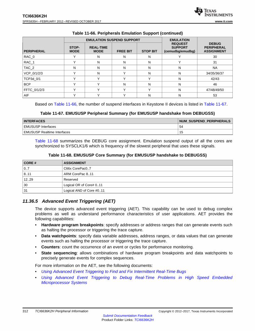
312
TCI6636K2HSPRS835H –FEBRUARY 2012–REVISED OCTOBER 2017 www.ti.com
Submit Documentation FeedbackProduct Folder Links: TCI6636K2H
TCI6636K2H Peripheral Information Copyright © 2012–2017, Texas Instruments Incorporated
Table 11-66. Peripherals Emulation Support (continued)
PERIPHERAL
EMULATION SUSPEND SUPPORT EMULATIONREQUESTSUPPORT
(cemudbg/emudbg)
DEBUGPERIPHERALASSIGNMENT
STOP-MODE
REAL-TIMEMODE FREE BIT STOP BIT
RAC_0 Y N N N Y 30RAC_1 Y N N N Y 31TAC_2 N N N N N NAVCP_0/1/2/3 Y N Y N N 34/35/36/37TCP3d_0/1 Y Y Y Y N 42/43BCP Y Y N N N 46FFTC_0/1/2/3 Y Y Y Y N 47/48/49/50AIF Y Y Y N N 53
Based on Table 11-66, the number of suspend interfaces in Keystone II devices is listed in Table 11-67.
Table 11-67. EMUSUSP Peripheral Summary (for EMUSUSP handshake from DEBUGSS)
INTERFACES NUM_SUSPEND_PERIPHERALSEMUSUSP Interfaces 54EMUSUSP Realtime Interfaces 15
Table 11-68 summarizes the DEBUG core assignment. Emulation suspend output of all the cores aresynchronized to SYSCLK1/6 which is frequency of the slowest peripheral that uses these signals.
Table 11-68. EMUSUSP Core Summary (for EMUSUSP handshake to DEBUGSS)
CORE # ASSIGNMENT0..7 C66x CorePac0..78..11 ARM CorePac 8..1112..29 Reserved30 Logical OR of Core# 0..1131 Logical AND of Core #0..11
11.36.5 Advanced Event Triggering (AET)The device supports advanced event triggering (AET). This capability can be used to debug complexproblems as well as understand performance characteristics of user applications. AET provides thefollowing capabilities:• Hardware program breakpoints: specify addresses or address ranges that can generate events such
as halting the processor or triggering the trace capture.• Data watchpoints: specify data variable addresses, address ranges, or data values that can generate
events such as halting the processor or triggering the trace capture.• Counters: count the occurrence of an event or cycles for performance monitoring.• State sequencing: allows combinations of hardware program breakpoints and data watchpoints to
precisely generate events for complex sequences.
For more information on the AET, see the following documents:• Using Advanced Event Triggering to Find and Fix Intermittent Real-Time Bugs• Using Advanced Event Triggering to Debug Real-Time Problems in High Speed Embedded
Microprocessor Systems

C
TPLH
A
B
3
1 2
A
C
B
BuffersBufferInputs
DP[n] /EMU[n] Pins
TPLH
313
TCI6636K2Hwww.ti.com SPRS835H –FEBRUARY 2012–REVISED OCTOBER 2017
Submit Documentation FeedbackProduct Folder Links: TCI6636K2H
TCI6636K2H Peripheral InformationCopyright © 2012–2017, Texas Instruments Incorporated
11.36.6 TraceThe device supports trace. Trace is a debug technology that provides a detailed, historical account ofapplication code execution, timing, and data accesses. Trace collects, compresses, and exports debuginformation for analysis. Trace works in real-time and does not impact the execution of the system.
For more information on board design guidelines for trace advanced emulation, see the Emulation andTrace Headers Technical Reference Manual.
11.36.6.1 Trace Electrical Data and Timing
The Trace switching characteristics are shown in Table 11-69.
Table 11-69. Trace Switching Characteristics(see Figure 11-62)NO. PARAMETER MIN MAX UNIT1 tw(DPnH) Pulse duration, DPn/EMUn high 2.4 ns1 tw(DPnH)90% Pulse duration, DPn/EMUn high detected at 90% Voh 1.5 ns2 tw(DPnL) Pulse duration, DPn/EMUn low 2.4 ns2 tw(DPnL)10% Pulse duration, DPn/EMUn low detected at 10% Voh 1.5 ns3 tsko(DPn) Output skew time, time delay difference between DPn/EMUn pins
configured as trace -1 1 ns
tskp(DPn) Pulse skew, magnitude of difference between high-to-low (tphl) and low-to-high (tplh) propagation delays. 600 ps
tsldp_o(DPn) Output slew rate DPn/EMUn 3.3 V/ns
Figure 11-62. Trace Timing
11.36.7 IEEE 1149.1 JTAGThe Joint Test Action Group (JTAG) interface is used to support boundary scan and emulation of thedevice. The boundary scan supported allows for an asynchronous test reset (TRST) and only the fivebaseline JTAG signals (for example, no EMU[1:0]) required for boundary scan. Most interfaces on thedevice follow the Boundary Scan Test Specification (IEEE 1149.1), while all of the SerDes (SGMII)support the AC-coupled net test defined in AC-Coupled Net Test Specification (IEEE 1149.6).
It is expected that all compliant devices are connected through the same JTAG interface, in daisy-chainfashion, in accordance with the specification. The JTAG interface uses 1.8-V LVCMOS buffers, compliantwith the Power Supply Voltage and Interface Standard for Nonterminated Digital Integrated CircuitSpecification (EAI/JESD8-5).

314
TCI6636K2HSPRS835H –FEBRUARY 2012–REVISED OCTOBER 2017 www.ti.com
Submit Documentation FeedbackProduct Folder Links: TCI6636K2H
TCI6636K2H Peripheral Information Copyright © 2012–2017, Texas Instruments Incorporated
11.36.7.1 IEEE 1149.1 JTAG Compatibility Statement
For maximum reliability, the TCI6636K2H device includes an internal pulldown (IPD) on the TRST pin toensure that TRST will always be asserted upon power up and the device’s internal emulation logic willalways be properly initialized when this pin is not routed out. JTAG controllers from Texas Instrumentsactively drive TRST high. However, some third-party JTAG controllers may not drive TRST high, butexpect the use of an external pullup resistor on TRST. When using this type of JTAG controller, assertTRST to initialize the device after powerup and externally drive TRST high before attempting anyemulation or boundary scan operations.

TDI / TMS
1a
1
3
TCK
4
TDO
1b
2
315
TCI6636K2Hwww.ti.com SPRS835H –FEBRUARY 2012–REVISED OCTOBER 2017
Submit Documentation FeedbackProduct Folder Links: TCI6636K2H
TCI6636K2H Peripheral InformationCopyright © 2012–2017, Texas Instruments Incorporated
11.36.7.2 JTAG Electrical Data and Timing
JTAG test port timing requirements are shown in Table 11-70 and JTAG test port switching characteristicsare shown in Table 11-71.
Table 11-70. JTAG Test Port Timing Requirements(see Figure 11-63)NO. MIN MAX UNIT1 tc(TCK) Cycle time, TCK 23 ns1a tw(TCKH) Pulse duration, TCK high (40% of tc) 9.2 ns1b tw(TCKL) Pulse duration, TCK low (40% of tc) 9.2 ns3 tsu(TDI-TCK) Input setup time, TDI valid to TCK high 2 ns3 tsu(TMS-TCK) Input setup time, TMS valid to TCK high 2 ns4 th(TCK-TDI) Input hold time, TDI valid from TCK high 10 ns4 th(TCK-TMS) Input hold time, TMS valid from TCK high 10 ns
Table 11-71. JTAG Test Port Switching Characteristics(see Figure 11-63)NO. PARAMETER MIN MAX UNIT2 td(TCKL-TDOV) Delay time, TCK low to TDO valid 8.24 ns
Figure 11-63. JTAG Test-Port Timing

316
TCI6636K2HSPRS835H –FEBRUARY 2012–REVISED OCTOBER 2017 www.ti.com
Submit Documentation FeedbackProduct Folder Links: TCI6636K2H
Device and Documentation Support Copyright © 2012–2017, Texas Instruments Incorporated
12 Device and Documentation Support
12.1 Device NomenclatureTo designate the stages in the product development cycle, TI assigns prefixes to the part numbers of alldevices and support tools. Each family member has one of two prefixes: X or [blank]. These prefixesrepresent evolutionary stages of product development from engineering prototypes through fully qualifiedproduction devices/tools.
Device development evolutionary flow:• X: Experimental device that is not necessarily representative of the final device's electrical
specifications• [Blank]: Fully qualified production device
Support tool development evolutionary flow:• X: Development-support product that has not yet completed Texas Instruments internal qualification
testing.• [Blank]: Fully qualified development-support product
Experimental (X) and fully qualified [Blank] devices and development-support tools are shipped with thefollowing disclaimer:
Developmental product is intended for internal evaluation purposes.
Fully qualified and production devices and development-support tools have been characterized fully, andthe quality and reliability of the device have been demonstrated fully. TI's standard warranty applies.
Predictions show that experimental devices (X) have a greater failure rate than the standard productiondevices. Texas Instruments recommends that these devices not be used in any production systembecause their expected end-use failure rate still is undefined. Only qualified production devices are to beused.
TI device nomenclature also includes a suffix with the device family name. This suffix indicates thepackage type (for example, AAW), the temperature range (for example, blank is the default casetemperature range), and the device speed range, in Megahertz (for example, blank is 1000 MHz [1 GHz]).
For device part numbers and further ordering information for TCI6636K2H in the AAW package type, seeti.com or contact your TI sales representative.
Figure 12-1 provides a legend for reading the complete device name for any C66x+ DSP generationmember.

PREFIX
X = Experimental deviceBlank = Qualified device
DEVICE FAMILY
TCI = System on Chip
PACKAGE TYPE
AAW = 1517-pin plastic ball grid array,with Pb-free solder balls and die bumps
DEVICE SPEED RANGE
Blank = 1 GHz
2 = 1.2 GHz
ARCHITECTURE
K2 = KeyStone II
Blank = Initial 1.0 silicon
SILICON REVISION
DEVICE CORE
66 = C66 DSP Family
DEVICE NUMBER
36
PLATFORM
H
TEMPERATURE RANGE
A = Extended temperature range (–40°C to +100°C)Blank = 0°C to +100°C (default case temperature)
TCI 66 AAW( _ )36 K2 H ( _ ) ( _ ) ( _ )( _ )
SECURITY
A = Silicon Revision 1.1B = Silicon Revision 2.0C = Silicon Revision 3.0D = Silicon Revision 3.1
24 = 1.2-GHz DSP / 1.4-GHz ARM
Blank = Security Accelerator disabled / General-Purpose deviceX = Security Accelerator enabled / General-Purpose device
D = Security Accelerator enabled / High-Security devicewith TI developmental keys
S = Security Accelerator enabled / High-Security devicewith production keys
317
TCI6636K2Hwww.ti.com SPRS835H –FEBRUARY 2012–REVISED OCTOBER 2017
Submit Documentation FeedbackProduct Folder Links: TCI6636K2H
Device and Documentation SupportCopyright © 2012–2017, Texas Instruments Incorporated
Figure 12-1. C66x DSP Device Nomenclature (Including the TCI6636K2H Device)

318
TCI6636K2HSPRS835H –FEBRUARY 2012–REVISED OCTOBER 2017 www.ti.com
Submit Documentation FeedbackProduct Folder Links: TCI6636K2H
Device and Documentation Support Copyright © 2012–2017, Texas Instruments Incorporated
12.2 Tools and SoftwareTI offers and extensive line of development tools. Tools and software to evaluate the performance of thedevice, generate code, and develop solutions are listed below.
ModelsTCI6636K2H and TCI6635K2H 1149.1 AAW BSDL Model BSDL model for the TCI6636K2H DSP.TCI6636K2H and TCI6635K2H 1149.6 AAW BSDL Model BSDL model for the TCI6636K2H DSP.TCI6636K2H and TCI6635K2H AAW IBIS Model IBIS model for the TCI6636K2H and TCI6635K2H
DSPs.
Design Kits and Evaluation ModulesTCI6636K2H Evaluation Module Enables developers to immediately start evaluating TCI6636K2H
processor and begin building application around it especially those demanding high-performance computation like telecom infrastructures, wireless standards includingWCDMA/HSPA/HSPA+, TD-SCDMA, GSM, TDD-LTE,FDD-LTE, and WiMAX.
SoftwareSYS/BIOS and Linux Multicore Software Development Kits (MCSDK) for C66x, C647x, C645x
ProcessorsProvides highly-optimized bundles of foundational, platform-specific drivers to enabledevelopment on selected TI ARM and DSP devices. The MCSDK gives developers theability to evaluate hardware and software capabilities of the evaluation platform and torapidly develop applications.
Development ToolsCode Composer Studio (CCS) Integrated Development Environment (IDE) for Multicore Processors
Integrated development environment (IDE) that supports TI's Microcontroller and EmbeddedProcessors portfolio. Code Composer Studio comprises a suite of tools used to develop anddebug embedded applications. It includes an optimizing C/C++ compiler, source code editor,project build environment, debugger, profiler, and many other features. The intuitive IDEprovides a single user interface taking you through each step of the application developmentflow. Familiar tools and interfaces allow users to get started faster than ever before. CodeComposer Studio combines the advantages of the Eclipse software framework withadvanced embedded debug capabilities from TI resulting in a compelling feature-richdevelopment environment for embedded developers.
XDS200 USB Debug Probe Features a balance of low cost with good performance between the superlow cost XDS100 and the high performance XDS560v2. Also, all XDS debug probes supportCore and System Trace in all ARM and DSP processors that feature an Embedded TraceBuffer (ETB).
XDS560v2 System Trace USB & Ethernet Debug Probe Adds system pin trace in its large externalmemory buffer. Available for selected TI devices, this external memory buffer capturesdevice-level information that allows obtaining accurate bus performance activity andthroughput, as well as power management of core and peripherals. Also, all XDS debugprobes support Core and System Trace in all ARM and DSP processors that feature anEmbedded Trace Buffer (ETB).
XDS560v2 System Trace USB Debug Probe Connects to the target board via a MIPI HSPT 60-pinconnector (with multiple adapters for TI 14-pin, TI 20-pin and ARM 20 pin) and to the hostPC via USB2.0 High speed (480Mbps). It also requires a license of Code Composer StudioIDE running on the host PC.

319
TCI6636K2Hwww.ti.com SPRS835H –FEBRUARY 2012–REVISED OCTOBER 2017
Submit Documentation FeedbackProduct Folder Links: TCI6636K2H
Device and Documentation SupportCopyright © 2012–2017, Texas Instruments Incorporated
TI Design NetworkKeystone II SoC Solution Provides a complete stack of operating system and communications software
for the TI Keystone II architecture. It includes a Yocto based commercial Linux distribution,DSP operating system (OSEck®) and an optimized communication service between ARMcores, DSP cores, and external CPUs in the system (LINX).
OSEck Provides a full-featured, compact, real-time kernel for DSPs that is optimized to suit thespecific requirements of high performance, memory constrained applications. OSEck is acompact kernel and has an extremely small memory footprint, but still combines richfunctionality with high performance and true real-time behavior.
12.3 Documentation SupportTo receive notification of documentation updates, navigate to the device product folder on ti.com(TCI6636K2H). In the upper right corner, click on Alert me to register and receive a weekly digest of anyproduct information that has changed. For change details, review the revision history included in anyrevised document.
The current documentation that describes the DSP, related peripherals, and other technical collateral islisted below.
ErrataTCI6636K2H Multicore DSP+ARM KeyStone II SOC Silicon Errata
Describes the silicon updates to the functional specifications for the TCI6636K2H fixed- andfloating-point digital signal processor.
Application ReportsSERDES Link Commissioning on KeyStone I and II Devices
Explains the SerDes transmit and receive parameters tuning, tools and some debugtechniques for TI Keystone I and Keystone II devices.
Keystone II DDR3 Debug GuideProvides tools for use when debugging a failing DDR3 interface on a KeyStone II device.
KeyStone I-to-KeyStone II Migration GuideDescribes the main System-on-Chip (SoC) level and peripheral changes that need to beconsidered when migrating a KeyStone I-based system design to a KeyStone II-basedsystem design.
Keystone II DDR3 InitializationProvides a step-to-step initialization guide for the Keystone II device DDR3 SDRAMcontroller.
DDR3 Design Requirements for KeyStone DevicesProvides implementation instructions for the DDR3 interface incorporated in the TI KeyStoneseries of DSP devices. The DDR3 interface supports 1600 MT/s and lower memory speedsin a variety of topologies.
Hardware Design Guide for KeyStone II DevicesDescribes hardware system design considerations for the KeyStone II family of processors.This design guide is intended to be used as an aid during the development of applicationhardware. Other aids including, but not limited to, device data manuals and explicit collateralshould also be used.
Ethernet Packet Transfer Via Fast C&M Over AIF2Discusses the implementation of Ethernet packet transfer through Fast Control andManagement (Fast C&M) over AIF2.
User's GuidesKeyStone Architecture Phase Locked Loop (PLL) Controller User's Guide
Describes the operation of the KeyStone software-programmable phase-locked loop (PLL)Controller. The PLL Controller offers flexibility and convenience by way of software-configurable multipliers and dividers to modify the input signal internally. The resulting clockoutputs are passed to the CorePacs, peripherals, and other modules inside the device.
KeyStone II Architecture Serializer/Deserializer (SerDes) User's Guide

320
TCI6636K2HSPRS835H –FEBRUARY 2012–REVISED OCTOBER 2017 www.ti.com
Submit Documentation FeedbackProduct Folder Links: TCI6636K2H
Device and Documentation Support Copyright © 2012–2017, Texas Instruments Incorporated
The SerDes performs serial-to-parallel conversions on data received from a peripheraldevice and parallel-to-serial conversion on data received from the CPU. The SerDesincludes control capability and a processor interrupt system that can be tailored to minimizesoftware management of the communications link.
KeyStone Architecture Enhanced Direct Memory Access 3 (EDMA3) User's GuideDescribes the Enhanced Direct Memory Access (EDMA3) controller. The primary purpose ofthe EDMA3 controller is to service data transfers that you program between two memory-mapped slave endpoints on the device.
KeyStone Architecture Bit Rate Coprocessor (BCP) User's GuideDescribes the architecture and use of the BCP peripheral.
KeyStone Architecture Multicore Navigator User's GuideDescribes the functionality, operational details, and programming information for thePKTDMA and the components of the QMSS in KeyStone architecture devices.
Keystone II Architecture DDR3 Memory Controller User's GuideDescribes how the DDR3 memory controller is used to interface with JESD79-3C standardcompliant SDRAM devices. Memory types such as DDR1 SDRAM, DDR2 SDRAM, SDRSDRAM, SBSRAM, and asynchronous memories are not supported. The DDR3 memorycontroller SDRAM can be used for program and data storage.
Keystone II Architecture Fast Fourier Transform Coprocessor (FFTC) User's GuideDescribes the functionality and operation of the FFTC module. The FFTC module isaccessible across all the C66x cores on a multicore DSP. This module can be used toaccelerate the FFT and IFFT computations that are required in various applications like testand measurement, avionics, and wireless LTE systems.
KeyStone II Architecture Antenna Interface 2 (AIF2) User's GuideDescribes the AIF2 peripheral module that supports transfers of baseband IQ data betweenuplink and downlink baseband DSP processors and a high-speed serial interface.
KeyStone Architecture Power Sleep Controller (PSC) User's GuideDescribes the functionality, operational details, and programming information for the PowerSleep Controller (PSC) module in KeyStone architecture devices.
KeyStone II Architecture Universal Serial Bus 3.0 (USB 3.0) User's GuideDescribes the features, architecture, and details of the Universal Serial Bus 3.0 (USB 3.0)peripheral.
KeyStone Architecture Peripheral Component Interconnect Express (PCIe) User's GuideDescribes the features, architecture, and details of the Peripheral Component InterconnectExpress (PCIe).
KeyStone II Architecture Debug and Trace User's GuideDescribes the capabilities of the trace features available through the debug architecture onKeyStone devices. Trace information can be gathered at the DSP core level or at the systemlevel. The Debug Subsystem captures and exports trace data for both levels of trace. Traceis implemented as a nonintrusive debug tool within the KeyStone architecture, but can beselected to operate in both intrusive and nonintrusive mode depending on the amount ofdata the user wants to export.
KeyStone II Architecture ARM Bootloader User's GuideDescribes the features of the on-chip bootloader provided with the ARM Cortex-A15processor.
KeyStone Architecture DSP Bootloader User's GuideDescribes the features of the on-chip bootloader provided with C66x_Digital SignalProcessors (DSP).
KeyStone Architecture Gigabit Ethernet (GbE) Switch Subsystem User's GuideGives a functional description of the Ethernet Switch Subsystem and related portions of theSerializer/Deserializer (SerDes) module. The Ethernet Switch Subsystem consists of theEthernet Media Access Controller (EMAC) module, Serial Gigabit Media IndependentInterface (SGMII) modules, Physical Layer (PHY) device Management Data Input/Output(MDIO) module, Ethernet Switch module, and other associated submodules that areintegrated on the device.
TMS320C66x DSP CorePac User's GuideProvides an overview of the main components and features of the C66x CorePac.

321
TCI6636K2Hwww.ti.com SPRS835H –FEBRUARY 2012–REVISED OCTOBER 2017
Submit Documentation FeedbackProduct Folder Links: TCI6636K2H
Device and Documentation SupportCopyright © 2012–2017, Texas Instruments Incorporated
KeyStone Architecture Memory Protection Unit (MPU) User's GuideDescribes the functionality, operational details, and programming information for theKeyStone Architecture Memory Protection Unit (MPU).
KeyStone Architecture HyperLink User's GuideProvides a high-speed, low-latency, and low-pin-count communication interface that extendsthe internal CBA 3.x-based transactions between two KeyStone devices.
KeyStone Architecture Security Accelerator (SA) User's GuideProvides hardware engines to perform encryption, decryption, and authentication operationson packets for commonly supported protocols, including IPsec ESP and AH, SRTP, and AirCipher. The SA also provides the hardware modules to assist the host in generating publickeys and random numbers.
KeyStone II Architecture Multicore Shared Memory Controller (MSMC) User's GuideThe MSMC manages traffic among ARM CorePacs, multiple C66x CorePacs, DMA, othermastering peripherals, and the EMIF in a multicore device. MSMC also provides a sharedon-chip SRAM that is accessible by all the CorePacs and the mastering peripherals on thedevice. MSMC provides memory protection for accesses to the MSMC SRAM and DDR3memory from system masters.
KeyStone Architecture Serial Rapid IO (SRIO) User's GuideDescribes the general operation of SRIO, how this module is connected to the outside world,the features supported, SRIO registers, and examples of channel and queue operations.
KeyStone II Architecture ARM CorePac User's GuideDescribes the ARM CorePac in the KeyStone II Architecture, but it does not describe thedetails of the ARM core itself.
KeyStone Architecture Packet Accelerator (PA) User's GuideOne of the main components of the network coprocessor (NETCP) peripheral, the PA workstogether with the security accelerator (SA) and the gigabit Ethernet switch subsystem to forma network processing solution. The purpose of PA in the NETCP is to perform packetprocessing operations such as packet header classification, checksum generation, andmultiqueue routing.
KeyStone Architecture Semaphore2 Hardware Module User's GuideDescribes the operation of the Semaphore2 hardware module. The semaphore2 module isaccessible across all the cores on a multicore DSP.

322
TCI6636K2HSPRS835H –FEBRUARY 2012–REVISED OCTOBER 2017 www.ti.com
Submit Documentation FeedbackProduct Folder Links: TCI6636K2H
Device and Documentation Support Copyright © 2012–2017, Texas Instruments Incorporated
KeyStone Architecture Serial Peripheral Interface (SPI) User's GuideDescribes the features, architecture and registers associated with the serial peripheralinterface (SPI) module.
KeyStone Architecture Chip Interrupt Controller (CIC) User's GuideDescribes the functionality, operational details, and programming information for theKeyStone Architecture Chip Interrupt Controller (CIC).
KeyStone Architecture Timer 64P User's GuideProvides an overview of the 64-bit timer in the KeyStone Architecture devices. The timer canbe configured as a general-purpose 64-bit timer, dual general-purpose 32-bit timers, or awatchdog timer. When configured as dual 32-bit timers, each half can operate in conjunction(chain mode) or independently (unchained mode) of each other.
KeyStone Architecture Inter-IC control Bus (I2C) User's GuideDescribes the inter-integrated circuit (I2C) module in the KeyStone Architecture Digital SignalProcessor (DSP). The I2C provides an interface between the KeyStone device and otherdevices compliant with Philips Semiconductors Inter-IC bus (I2C-bus) specification version2.1 and connected by way of an I2C-bus. This document assumes the reader is familiar withthe I2C-bus specification.
Keystone Architecture Viterbi Coprocessor (VCP2) User's GuideDescribes the operation and programming of the Viterbi Coprocessor 2 (VCP2).
KeyStone Architecture External Memory Interface (EMIF16) User's GuideDescribes the operation of the External Memory Interface (EMIF16) module in the KeyStoneDSP family (refer to the device data manual for applicability to a particular part). The EMIF16module is accessible across all the cores and all system masters that are not cores.
KeyStone Architecture Turbo Decoder Coprocessor 3 (TCP3d) User's GuideDescribes the functionality, operational details, and programming information for the Turbo-Decoder Coprocessor 3 (TCP3D) in KeyStone architecture devices.
TMS320C66x DSP Cache User's GuideDescribes how the cache-based memory system of the C66x DSP can be efficiently used inDSP applications. The internal memory architecture of these devices is organized in a two-level hierarchy consisting of a dedicated program memory (L1P) and a dedicated datamemory (L1D) on the first level. Accesses by the core to the these first level memories cancomplete without core pipeline stalls.
KeyStone Architecture General-Purpose Input/Output (GPIO) User's GuideDescribes the general-purpose input/output (GPIO) peripheral in the KeyStone digital signalprocessors (DSPs).
KeyStone Architecture Universal Asynchronous Receiver/Transmitter (UART) User's GuidePerforms serial-to-parallel conversions on data received from a peripheral device andparallel-to-serial conversion on data received from the CPU. The UART includes controlcapability and a processor interrupt system that can be tailored to minimize softwaremanagement of the communications link.
TMS320C66x DSP CPU and Instruction Set Reference GuideDescribes the CPU architecture, pipeline, instruction set, and interrupts of the C66x DSP.
KeyStone Architecture Network Coprocessor (NETCP) User's GuideDescribes the network coprocessor (NETCP) hardware accelerator that processes datapackets with a main focus on processing Ethernet packets. NETCP has two gigabit Ethernet(GbE) modules to send and receive packets from an IEEE 802.3 compliant network, apacket accelerator (PA) to perform packet classification operations such as header matching,and packet modification operations such as checksum generation, A and a securityaccelerator (SA) to encrypt and decrypt data packets.

323
TCI6636K2Hwww.ti.com SPRS835H –FEBRUARY 2012–REVISED OCTOBER 2017
Submit Documentation FeedbackProduct Folder Links: TCI6636K2H
Device and Documentation SupportCopyright © 2012–2017, Texas Instruments Incorporated
White PapersMulticore SoCs Stay a Step Ahead of SoC FPGAs
Describes the differences between SoCs and FPGAs. Recently, the integration of ARMCortex-A cores into FPGAs and compute-intense cores could lead one to believe that thepaths of true multicore SoCs and these so-called FPGA SoCs had converged. A closerexamination reveals that in reality they are still very far apart and that true multicore SoCsoffer increasing advantages in those critical areas required by today’s demanding products.
Optimizing Modern Radar Systems Using Low-Latency, High-Performance FFT CoprocessorsSimulates the implementation of a synthetic aperture radar (SAR) system on a TI multicoreSoC in order to compare the FFTC performance to single-precision (SP) floating-point FFTimplementations and show that there is no appreciable performance loss due to theprecision of the FFTC.
Illuminating the Buildout of Heterogeneous Networks (HetNets) With Small Cell SoCsDescribes how the TCI6630K2L SoC enhances networking connectivity with a built-inEthernet switch and a Digital Radio Front End (DRFE) to reduce total power consumptionand cost of ownership.
Accelerate Multicore Application Development with KeyStone SoftwareExplores how Texas Instruments KeyStone multicore SoCs offload many software functionsinto hardware AccelerationPacs or other architectural elements to reduce the amount ofsoftware needed and to automate many of the more complex multicore management tasks.
Embracing LTE-A With KeyStone SoCsDiscusses the major elements of the LTE-A standard and how it achieves higher throughputwith increased efficiencies, as well as how LTE-A is addressed in TI’s KeyStone multicoreSoC architecture.
Paving the Path for Wireless Capacity ExpansionExplores some of the techniques that operators can use to increase capacity and theirrelative costs. This paper also discusses how TI's new wireless SoC plays a key role inenabling manufacturers to meet this capacity challenge.
Building Heterogeneous Networks of Green Base Stations on TI’s KeyStone II ArchitectureBuilding on a decade of successfully providing macro base station digital basebanddeployments to more than 200 wireless service providers and operators worldwide, TexasInstruments is again stepping up to deliver its next-generation KeyStone II architecture whichwill enable integrated, scalable and low-power solutions for tomorrow’s heterogeneous andgreen wireless network.
Maximizing Multicore Efficiency With Navigator RuntimeDescribes how TI's innovative KeyStone II multicore architecture is designed to simplifymulticore programmability by providing specialized hardware to facilitate scheduling and loadbalancing. Through these facilities, KeyStone II has achieved a performance breakthrough inmulticore programming.
Design FilesKeystone II Flotherm Thermal Model
The Flotherm thermal models contained within this compressed file are suitable for variouspower configurations and should scale properly within the allowable configuration limits.
Keystone II IcePak Thermal ModelThe IcePak thermal models contained within this compressed file are suitable for variouspower configurations and should scale properly within the allowable configuration limits.

324
TCI6636K2HSPRS835H –FEBRUARY 2012–REVISED OCTOBER 2017 www.ti.com
Submit Documentation FeedbackProduct Folder Links: TCI6636K2H
Device and Documentation Support Copyright © 2012–2017, Texas Instruments Incorporated
Other DocumentsTMS320TCI6636 SoC High-Performance SoC for Ultra-High Capacity Small Cells and Green-Power
Macro CellsDescribes how the TCI6636 SoC is ideally suited to the data-centric performance thatwireless network operators are demanding today for 4G small-cell base stations andprovides the power to help the operator migrate to future standards.
12.4 Community ResourcesThe following links connect to TI community resources. Linked contents are provided "AS IS" by therespective contributors. They do not constitute TI specifications and do not necessarily reflect TI's views;see TI's Terms of Use.TI E2E™ Online Community The TI engineer-to-engineer (E2E) community was created to foster
collaboration among engineers. At e2e.ti.com, you can ask questions, share knowledge,explore ideas and help solve problems with fellow engineers.
TI Embedded Processors Wiki Established to help developers get started with Embedded Processorsfrom Texas Instruments and to foster innovation and growth of general knowledge about thehardware and software surrounding these devices.
12.5 TrademarksKeyStone, SmartReflex, C6000, E2E are trademarks of Texas Instruments.MPCore, NEON, CoreSight, ARM7 are trademarks of ARM Ltd or its subsidiaries.ARM, Cortex, Jazelle, Thumb are registered trademarks of ARM Ltd or its subsidiaries.Windows is a registered trademark of Microsoft Corp.All other trademarks are the property of their respective owners.
12.6 Electrostatic Discharge CautionThis integrated circuit can be damaged by ESD. Texas Instruments recommends that all integrated circuits be handled withappropriate precautions. Failure to observe proper handling and installation procedures can cause damage.
ESD damage can range from subtle performance degradation to complete device failure. Precision integrated circuits may be moresusceptible to damage because very small parametric changes could cause the device not to meet its published specifications.
12.7 GlossaryTI Glossary This glossary lists and explains terms, acronyms, and definitions.

325
TCI6636K2Hwww.ti.com SPRS835H –FEBRUARY 2012–REVISED OCTOBER 2017
Submit Documentation FeedbackProduct Folder Links: TCI6636K2H
Mechanical, Packaging, and Orderable InformationCopyright © 2012–2017, Texas Instruments Incorporated
13 Mechanical, Packaging, and Orderable Information
13.1 Packaging InformationThe following pages include mechanical, packaging, and orderable information. This information is themost current data available for the designated devices. This data is subject to change without notice andrevision of this document. For browser-based versions of this data sheet, refer to the left-hand navigation.


IMPORTANT NOTICE
Texas Instruments Incorporated (TI) reserves the right to make corrections, enhancements, improvements and other changes to itssemiconductor products and services per JESD46, latest issue, and to discontinue any product or service per JESD48, latest issue. Buyersshould obtain the latest relevant information before placing orders and should verify that such information is current and complete.TI’s published terms of sale for semiconductor products (http://www.ti.com/sc/docs/stdterms.htm) apply to the sale of packaged integratedcircuit products that TI has qualified and released to market. Additional terms may apply to the use or sale of other types of TI products andservices.Reproduction of significant portions of TI information in TI data sheets is permissible only if reproduction is without alteration and isaccompanied by all associated warranties, conditions, limitations, and notices. TI is not responsible or liable for such reproduceddocumentation. Information of third parties may be subject to additional restrictions. Resale of TI products or services with statementsdifferent from or beyond the parameters stated by TI for that product or service voids all express and any implied warranties for theassociated TI product or service and is an unfair and deceptive business practice. TI is not responsible or liable for any such statements.Buyers and others who are developing systems that incorporate TI products (collectively, “Designers”) understand and agree that Designersremain responsible for using their independent analysis, evaluation and judgment in designing their applications and that Designers havefull and exclusive responsibility to assure the safety of Designers' applications and compliance of their applications (and of all TI productsused in or for Designers’ applications) with all applicable regulations, laws and other applicable requirements. Designer represents that, withrespect to their applications, Designer has all the necessary expertise to create and implement safeguards that (1) anticipate dangerousconsequences of failures, (2) monitor failures and their consequences, and (3) lessen the likelihood of failures that might cause harm andtake appropriate actions. Designer agrees that prior to using or distributing any applications that include TI products, Designer willthoroughly test such applications and the functionality of such TI products as used in such applications.TI’s provision of technical, application or other design advice, quality characterization, reliability data or other services or information,including, but not limited to, reference designs and materials relating to evaluation modules, (collectively, “TI Resources”) are intended toassist designers who are developing applications that incorporate TI products; by downloading, accessing or using TI Resources in anyway, Designer (individually or, if Designer is acting on behalf of a company, Designer’s company) agrees to use any particular TI Resourcesolely for this purpose and subject to the terms of this Notice.TI’s provision of TI Resources does not expand or otherwise alter TI’s applicable published warranties or warranty disclaimers for TIproducts, and no additional obligations or liabilities arise from TI providing such TI Resources. TI reserves the right to make corrections,enhancements, improvements and other changes to its TI Resources. TI has not conducted any testing other than that specificallydescribed in the published documentation for a particular TI Resource.Designer is authorized to use, copy and modify any individual TI Resource only in connection with the development of applications thatinclude the TI product(s) identified in such TI Resource. NO OTHER LICENSE, EXPRESS OR IMPLIED, BY ESTOPPEL OR OTHERWISETO ANY OTHER TI INTELLECTUAL PROPERTY RIGHT, AND NO LICENSE TO ANY TECHNOLOGY OR INTELLECTUAL PROPERTYRIGHT OF TI OR ANY THIRD PARTY IS GRANTED HEREIN, including but not limited to any patent right, copyright, mask work right, orother intellectual property right relating to any combination, machine, or process in which TI products or services are used. Informationregarding or referencing third-party products or services does not constitute a license to use such products or services, or a warranty orendorsement thereof. Use of TI Resources may require a license from a third party under the patents or other intellectual property of thethird party, or a license from TI under the patents or other intellectual property of TI.TI RESOURCES ARE PROVIDED “AS IS” AND WITH ALL FAULTS. TI DISCLAIMS ALL OTHER WARRANTIES ORREPRESENTATIONS, EXPRESS OR IMPLIED, REGARDING RESOURCES OR USE THEREOF, INCLUDING BUT NOT LIMITED TOACCURACY OR COMPLETENESS, TITLE, ANY EPIDEMIC FAILURE WARRANTY AND ANY IMPLIED WARRANTIES OFMERCHANTABILITY, FITNESS FOR A PARTICULAR PURPOSE, AND NON-INFRINGEMENT OF ANY THIRD PARTY INTELLECTUALPROPERTY RIGHTS. TI SHALL NOT BE LIABLE FOR AND SHALL NOT DEFEND OR INDEMNIFY DESIGNER AGAINST ANY CLAIM,INCLUDING BUT NOT LIMITED TO ANY INFRINGEMENT CLAIM THAT RELATES TO OR IS BASED ON ANY COMBINATION OFPRODUCTS EVEN IF DESCRIBED IN TI RESOURCES OR OTHERWISE. IN NO EVENT SHALL TI BE LIABLE FOR ANY ACTUAL,DIRECT, SPECIAL, COLLATERAL, INDIRECT, PUNITIVE, INCIDENTAL, CONSEQUENTIAL OR EXEMPLARY DAMAGES INCONNECTION WITH OR ARISING OUT OF TI RESOURCES OR USE THEREOF, AND REGARDLESS OF WHETHER TI HAS BEENADVISED OF THE POSSIBILITY OF SUCH DAMAGES.Unless TI has explicitly designated an individual product as meeting the requirements of a particular industry standard (e.g., ISO/TS 16949and ISO 26262), TI is not responsible for any failure to meet such industry standard requirements.Where TI specifically promotes products as facilitating functional safety or as compliant with industry functional safety standards, suchproducts are intended to help enable customers to design and create their own applications that meet applicable functional safety standardsand requirements. Using products in an application does not by itself establish any safety features in the application. Designers mustensure compliance with safety-related requirements and standards applicable to their applications. Designer may not use any TI products inlife-critical medical equipment unless authorized officers of the parties have executed a special contract specifically governing such use.Life-critical medical equipment is medical equipment where failure of such equipment would cause serious bodily injury or death (e.g., lifesupport, pacemakers, defibrillators, heart pumps, neurostimulators, and implantables). Such equipment includes, without limitation, allmedical devices identified by the U.S. Food and Drug Administration as Class III devices and equivalent classifications outside the U.S.TI may expressly designate certain products as completing a particular qualification (e.g., Q100, Military Grade, or Enhanced Product).Designers agree that it has the necessary expertise to select the product with the appropriate qualification designation for their applicationsand that proper product selection is at Designers’ own risk. Designers are solely responsible for compliance with all legal and regulatoryrequirements in connection with such selection.Designer will fully indemnify TI and its representatives against any damages, costs, losses, and/or liabilities arising out of Designer’s non-compliance with the terms and provisions of this Notice.
Mailing Address: Texas Instruments, Post Office Box 655303, Dallas, Texas 75265Copyright © 2017, Texas Instruments Incorporated